JP2010092623A - Electronic breaker - Google Patents
Electronic breaker Download PDFInfo
- Publication number
- JP2010092623A JP2010092623A JP2008258815A JP2008258815A JP2010092623A JP 2010092623 A JP2010092623 A JP 2010092623A JP 2008258815 A JP2008258815 A JP 2008258815A JP 2008258815 A JP2008258815 A JP 2008258815A JP 2010092623 A JP2010092623 A JP 2010092623A
- Authority
- JP
- Japan
- Prior art keywords
- cpu
- reset signal
- circuit
- trip coil
- monitoring circuit
- Prior art date
- Legal status (The legal status is an assumption and is not a legal conclusion. Google has not performed a legal analysis and makes no representation as to the accuracy of the status listed.)
- Granted
Links
- 238000012544 monitoring process Methods 0.000 claims abstract description 26
- 230000004044 response Effects 0.000 claims abstract description 8
- 230000000737 periodic effect Effects 0.000 claims description 6
- 239000013256 coordination polymer Substances 0.000 description 7
- 238000004891 communication Methods 0.000 description 6
- 230000006870 function Effects 0.000 description 4
- 239000003990 capacitor Substances 0.000 description 3
- 238000001514 detection method Methods 0.000 description 2
- 238000010586 diagram Methods 0.000 description 2
- 230000005856 abnormality Effects 0.000 description 1
- 230000000903 blocking effect Effects 0.000 description 1
- 230000000694 effects Effects 0.000 description 1
- 238000005516 engineering process Methods 0.000 description 1
- 238000004519 manufacturing process Methods 0.000 description 1
- 238000000034 method Methods 0.000 description 1
- 230000007935 neutral effect Effects 0.000 description 1
- 238000011084 recovery Methods 0.000 description 1
- 230000008054 signal transmission Effects 0.000 description 1
Images


Landscapes
- Breakers (AREA)
Abstract
Description
本発明は、電路に過電流が流れたときに、CPUの制御によりトリップコイルを駆動して主接点を開く電子式ブレーカに関する。 The present invention relates to an electronic breaker that opens a main contact by driving a trip coil under the control of a CPU when an overcurrent flows in an electric circuit.
従来、電路に流れる電流を電流センサで検出し、電流センサの出力が閾値を超えたときに、CPUの制御によりトリップコイルを駆動して主接点を開く電子式ブレーカが知られている。CPU制御によると、遮断機能のほかに表示機能や通信機能などを容易に装備でき、ブレーカの機能性および機動性を高めることができる利点がある。 2. Description of the Related Art Conventionally, an electronic breaker that detects a current flowing in an electric circuit with a current sensor and drives a trip coil under the control of a CPU to open a main contact when an output of the current sensor exceeds a threshold value is known. According to the CPU control, in addition to the shut-off function, a display function, a communication function, and the like can be easily provided, and there is an advantage that the functionality and mobility of the breaker can be improved.
例えば、特許文献1には、記憶媒体に記録した定格電流をCPUに読み取らせ、ブレーカの内部メモリに登録する技術が記載されている。特許文献2には、ブレーカと外部操作機器との無線通信をCPUで制御し、定格電流を外部操作機器により無線通信を介して切り替える技術が記載されている。
ところが、従来の電子式ブレーカでは、CPUのフェイルセーフが確保されていなかった。このため、外来ノイズや雷サージなどでCPUが暴走したときに、電路に流れる電流を監視できなくなり、遮断機能に障害を来たし、二次被害を招くおそれがあった。 However, the conventional electronic breaker has not ensured failsafe of the CPU. For this reason, when the CPU runs away due to external noise or lightning surge, it becomes impossible to monitor the current flowing in the electric circuit, which may cause a failure in the interruption function and cause secondary damage.
そこで、本発明の目的は、CPUのフェイルセーフを確保し、暴走時の二次被害を未然に防止できる電子式ブレーカを提供することにある。 Therefore, an object of the present invention is to provide an electronic breaker that can ensure fail-safe CPU and prevent secondary damage during runaway.
上記課題を解決するために、本発明は、電路に流れる電流を電流センサで検出し、電流センサの出力が閾値を超えたときに、CPUの制御によりトリップコイルを駆動して主接点を開く電子式ブレーカにおいて、次のような手段を採用したことを特徴とする。 In order to solve the above-described problems, the present invention detects an electric current flowing in an electric circuit with a current sensor, and when the output of the current sensor exceeds a threshold value, the trip coil is driven under the control of the CPU to open the main contact. The type breaker is characterized by adopting the following means.
(1)CPUが出力する定期パルスに基づいてCPUの動作を監視する監視回路と、定期パルスが途絶えたときの監視回路の出力に応答してトリップコイルを駆動する駆動回路と備えたことを特徴とする電子式ブレーカ。 (1) A monitoring circuit that monitors the operation of the CPU based on a periodic pulse output from the CPU, and a drive circuit that drives the trip coil in response to the output of the monitoring circuit when the periodic pulse is interrupted. Electronic breaker.
(2)定期パルスが途絶えたときに、監視回路がCPUを初期化するためのリセット信号を出力し、駆動回路がCPUの初期化に要する時間よりも長い時間が経過した後にトリップコイルを駆動することを特徴とする電子式ブレーカ。 (2) When the periodic pulse is interrupted, the monitoring circuit outputs a reset signal for initializing the CPU, and the drive circuit drives the trip coil after a time longer than the time required for initialization of the CPU has elapsed. This is an electronic breaker.
(3)CPUの制御プログラムを記憶するメモリと、メモリに制御プログラムを書き込むときにリセット信号を遮断するスイッチとを備え、スイッチが遮断位置に操作されている状態で監視回路がリセット信号を出力したときに、駆動回路がトリップコイルを駆動することを特徴とする電子式ブレーカ。 (3) A memory for storing a control program for the CPU and a switch for shutting off the reset signal when the control program is written to the memory are provided, and the monitoring circuit outputs the reset signal while the switch is operated at the shut-off position. An electronic breaker characterized in that the drive circuit drives the trip coil.
上記(1)の電子式ブレーカによれば、監視回路が駆動回路と連系してCPUのフェイルセーフを確保するので、CPUの暴走に伴う二次被害を未然に防止できるという効果がある。 According to the electronic breaker of the above (1), the monitoring circuit is linked with the drive circuit to ensure the fail safe of the CPU, so that it is possible to prevent secondary damage accompanying the runaway of the CPU.
上記(2)の電子式ブレーカによれば、監視回路が出力したリセット信号でCPUを初期化し、初期化中に主接点をむやみに開くことなく、CPUを自動的に復旧できるという効果がある。 According to the electronic breaker of (2), there is an effect that the CPU can be automatically restored without initializing the main contact during initialization, by initializing the CPU with the reset signal output from the monitoring circuit.
上記(3)の電子式ブレーカによれば、スイッチを遮断位置に操作した状態で、CPUの制御プログラムをメモリに書き込むことができ、スイッチを遮断位置から戻し忘れたときに、駆動回路によりトリップコイルを駆動できるうえ、人為的なリセット信号に対するトリップコイルの応答に基づいて、スイッチの戻し忘れを容易に確認できるという効果がある。 According to the electronic breaker of (3) above, the CPU control program can be written into the memory while the switch is operated to the shut-off position, and when the switch is forgotten to return from the shut-off position, the trip coil is driven by the drive circuit. In addition, it is possible to easily check forgetting to return the switch based on the response of the trip coil to the artificial reset signal.
以下、本発明の実施形態を図面に基づいて説明する。図1は単相3線式電路用の電子式ブレーカの外観を示し、図2はケーシングの内部機構を示す。図3は電子式ブレーカの制御回路を示し、図4は制御回路中のCPU監視回路とトリップコイル駆動回路を詳細に示す。図5〜図8は監視回路と駆動回路の連係動作を示し、図5はCPU正常時、図6は過電流発生時、図7はCPU暴走時、図8はCPU復旧時の状態を示す。 Hereinafter, embodiments of the present invention will be described with reference to the drawings. FIG. 1 shows the external appearance of an electronic breaker for a single-phase three-wire circuit, and FIG. 2 shows the internal mechanism of the casing. FIG. 3 shows the control circuit of the electronic breaker, and FIG. 4 shows the CPU monitoring circuit and trip coil drive circuit in the control circuit in detail. 5 to 8 show the linking operation of the monitoring circuit and the drive circuit, FIG. 5 shows the state when the CPU is normal, FIG. 6 shows the state when an overcurrent occurs, FIG. 7 shows the state when the CPU is out of control, and FIG.
図1に示すように、この実施例の電子式ブレーカ1は、ケーシング2の上端部に3つの電源側端子3を備え、下端部に3つの負荷側端子4を備えている。ケーシング2の前面には、単相3線式電路を手動で開閉するハンドル5と、ブレーカ1の定格電流や動作状態を表示する表示部6と、表示や動作モードを切り替える手元スイッチ7と、パソコンや携帯端末等の外部操作機器に接続されるLAN配線接続口8とが設けられている。
As shown in FIG. 1, the
図2に示すように、ケーシング2の内部には、電路15(図3参照)に過電流が流れたときに主接点9を開くトリップコイル10と、電路15に短絡電流が流れたとときに主接点9を瞬時に開く瞬時遮断機構11と、トリップコイル10および瞬時遮断機構11の動力を主接点9に伝える開閉機構12とが設置されている。そして、ケーシング2の背面に電子回路基板13が取り付けられ、この基板13上に表示部6やトリップコイル10等を制御するための電子制御回路が設けられている。
As shown in FIG. 2, the
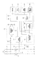
図3に示すように、単相3線式電路15は二本の電圧線15X,15Yと一本の中性線15Nとを備え、電圧線15X,15Y上に線路電流を検出する電流センサ16が設けられている。電子回路基板13には、電流センサ16の出力を数値化する電流検出回路17と、電流検出回路17の出力を監視するCPU18と、CPU18の動作電圧を主接点9より一次側(電源側)の電圧線15X,15Yから取得する制御電源回路19とが設けられている。制御電源回路19は、内部に異常が発生したときに、ヒューズ20を溶断し、CPU18等への電源の供給を停止するように構成されている。
As shown in FIG. 3, the single-phase three-wire
また、電子回路基板13には、主接点9より二次側(負荷側)の電圧線15X,15Yから取得した電圧(200V)でトリップコイル10を駆動するトリップコイル駆動回路21と、CPU18の動作を監視するCPU監視回路22と、赤外線リモコンを含む外部操作機器との通信を制御する通信制御部23と、外部のプログラム書込み装置が接続されるプログラム書込み接続部25と、プログラム書込みスイッチ26とが配設されている。CPU18は制御プログラムを記憶するフラッシュROM24を備えている。ROM24に制御プログラムを書き込むときには、書込みスイッチ26をプログラム書込み接続部25側に操作し(図3参照)、監視回路22の動作がCPU18に影響しないように、監視回路22が出力したリセット信号を遮断する。こうすれば、監視回路22の動作が無効となるので、制御プログラムをROM24に容易に書き込むことができる。書込み作業が終了したときには、スイッチ26を監視回路22と駆動回路21との接続点32側に操作し(図4参照)、リセット信号をCPU18に伝送できる状態に戻しておく。
The
図4に示すように、トリップコイル駆動回路21は、トリップコイル10を駆動するサイリスタSCRと、サイリスタSCRのゲートGに定電圧を印加するツェナーダイオードZDと、コンデンサCおよび抵抗RからなるCR遅延回路27と、CPU18の二つのデジタル出力端子P1,P2から出力された操作信号を受け取るD−FF(Dフリップフロップ)28と、D−FF28とサイリスタSCRを電気的に絶縁した状態でD−FF28の出力信号を中継するフォトカプラ29とが設けられている。フォトカプラ29は発光部29aと受光部29bとを備え、発光部29aの動作電圧が制御電源回路19(図3参照)から供給される。
As shown in FIG. 4, the trip
CPU監視回路22はWDT−IC(ウオッチドッグタイマIC)30を備え、CPU18がもう一つのデジタル出力端子P3からWDT−IC30のWD端子にクロックパルスCP(図5参照)を定期的に出力する。WDT−IC30のRST端子はD−FF28のCLK端子に接続されるとともに、書込みスイッチ26を介してCPU18のリセット端子に接続され、Tc端子が抵抗RとコンデンサCとに接続されている。WDT−IC30は、抵抗RとコンデンサCとで決まる時間中にクロックパルスCPがWD端子に与えられないときに、CPU18のクロックパルスCPが途絶えたと判断し、リセット信号をRST端子からCPU18とD−FF28とに出力する。そして、リセット信号に応答し、CPU18が制御プログラムのメインルーチンを実行して初期化作業を行うとともに、D−FF28がフォトカプラ29をOFFしてトリップコイル10を駆動するように構成されている。
The
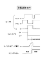
次に、上記のように構成された電子式ブレーカ1の動作について説明する。図5に示すように、CPU18が正常に動作しているときには、制御プログラムのメインルーチンでクロックパルスCPが出力端子P3からWDT−IC30のWD端子に定期的に出力される。このとき、Tc端子の電圧レベルはクロックパルスCPによりリセット信号の出力ライン(RST端子のLレベル)よりも低く抑えられ、RST端子がHレベルを維持し、リセット信号を出力しない。そして、電路15に正常な電流が流れている状態で、CPU18が出力端子P1,P2から操作パルスをD−FF28のCLR端子とPRE端子とに出力し、両方の端子を共にHレベルに維持し、Q端子をLレベルに保つ。これにより、フォトカプラ29がONし、サイリスタSCRがターンオフし、トリップコイル10が消磁し、主接点9が閉じた状態に保持される。
Next, the operation of the
図6に示すように、電路15に過電流が流れたときには、CPU18が出力端子P2側の操作パルスを停止し、D−FF28のPRE端子がH→Lレベルに切り替わり、Q端子がL→Hレベルに変化し、フォトカプラ29がOFFする。これにより、ツェナーダイオードZDの基準電圧がサイリスタSCRのゲートGに印加され、CR遅延回路27の設定時間(CR遅延時間)が経過した後にサイリスタSCRがターンオンし、トリップコイル10が主接点9を開く。そして、線路電流が消滅すると、CPU18が出力端子P1側の操作パルスを一時的に停止し、D−FF28のCLR端子をH→L→Hレベルに切り替え、CLR端子とPRE端子を共にHレベルに保った状態で、ハンドル5による主接点9の閉成操作を待つ。なお、CR遅延時間はCPU18の初期化に要する時間(図8参照)よりも長い値で設定されている
As shown in FIG. 6, when an overcurrent flows through the
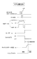
図7に示すように、CPU18が暴走し、クロックパルスCPが途絶えたときには、WDT−IC30において、Tc端子の電圧レベルがリセット信号の出力ラインまで上昇し、RST端子がH→Lレベルに切り替わり、リセット信号がRST端子から書込みスイッチ26を介してCPU18に出力される。そして、Tc端子の電圧レベルがリセット信号の停止ライン(0V)まで下降すると、RST端子がL→Hレベルに切り替わり、D−FF28のQ端子がL→Hレベルに変化し、フォトカプラ29がOFFする。この間、CPU18はリセット信号に応答して制御プログラムを再起動し、メインルーチンを実行してD−FF28をリセットする。
As shown in FIG. 7, when the
ここで、CPU18がメインルーチンを実行できないときには、D−FF28がリセットされず、Q端子がHレベルを維持し、フォトカプラ29がOFF状態を継続する。このため、サイリスタSCRがCR遅延時間の経過後にターンオンし、トリップコイル10が励磁し、主接点9が開放される。したがって、WDT−IC30のリセット信号でCPU18を初期化できないときに、トリップコイル10で電路15を遮断し、CPU18の暴走に伴う二次被害を未然に防止できる。また、施工者が制御プログラムを書き込んだ後に、書込みスイッチ26を閉じ忘れてリセット信号の遮断位置(図3に示す位置)に放置していた場合は、リセット信号がCPU18に伝送されず、D−FF28のCLK端子に入力され、Q端子がL→Hレベルに切り替わり、フォトカプラ29がOFFする。このため、スイッチ26を戻し忘れていた場合でも、トリップコイル10を駆動して、主接点9を確実に開くことができる。
Here, when the
図8に示すように、CPU18が初期化を実行できたときには、クロックパルスCPが立ち上がり、CPU18が正常な状態に復旧する。CPU18が復旧すると、WDT−IC30のTc端子の電圧レベルが上昇し、D−FF28のCLR端子がH→Lレベルに変化し、Q端子がH→Lレベルに切り替わり、D−FF28がリセットされ、フォトカプラ22がONする。このとき、駆動回路21のCR遅延回路27にCPU18の初期化に要する時間よりも長いCR遅延時間が設定されているため、サイリスタSCRのゲート電圧が上昇する前にフォトカプラ29がONし、サイリスタSCRはターンオンしない。したがって、CPU18の初期化中に主接点9をむやみに開くことなく、CPU18を自動的に復旧することができる。
As shown in FIG. 8, when the
また、CPU18を人為的に暴走状態とすることで、プログラム書込みスイッチ26の操作位置を容易に確認することができる。すなわち、CPU18のクロックパルスを意図的に停止し、WDT−IC30にリセット信号を出力させ、リセット信号に対するトリップコイル10の応答を確認する。施工者が書込みスイッチ26を閉じ忘れていた場合は、リセット信号がCPU18に伝送されず、図7に示すように、サイリスタSCRがターンオンしてトリップコイル10を駆動するので、施工者はハンドル5の突出状態を見て、スイッチ26の閉じ忘れを確認できる。書込みスイッチ26がリセット信号の伝送位置(図4に示す位置)に正しく閉じられていた場合は、リセット信号がCPU18に伝送され、図8に示すように、サイリスタSCRがターンオフしてトリップコイル10を駆動しないので、施工者はハンドル5の平伏状態を見て、スイッチ26の正規位置を確認できる。
Moreover, the operation position of the program write
なお、本発明は上記実施例に限定されるものではなく、以下に例示するように、本発明の趣旨を逸脱しない範囲で、各部の構成や形状を任意に変更して実施することも可能である。
(イ)CPU18が暴走したときに、監視回路22の出力に応答し、駆動回路21がトリップコイル10を直ちに駆動するように構成すること。
(ロ)制御プログラムを記憶するメモリをCPU18の外部に設置すること。
(ハ)CPU監視回路22を単相2線式電路や3相3線式電路用の電子式ブレーカに適用すること。
Note that the present invention is not limited to the above-described embodiments, and can be implemented by arbitrarily changing the configuration and shape of each part without departing from the spirit of the present invention, as exemplified below. is there.
(A) When the
(B) A memory for storing the control program is installed outside the
(C) The
1 電子式ブレーカ
9 主接点
10 トリップコイル
15 単相3線式電路
16 電流センサ
18 CPU
21 トリップコイル駆動回路
22 CPU監視回路
24 フラッシュROM
26 プログラム書込みスイッチ
27 CR遅延回路
1 Electronic breaker 9
21 Trip
26
Claims (3)
CPUが出力する定期パルスに基づいてCPUの動作を監視する監視回路と、定期パルスが途絶えたときの監視回路の出力に応答してトリップコイルを駆動する駆動回路と備えたことを特徴とする電子式ブレーカ。 In an electronic breaker that detects the current flowing in the electric circuit with a current sensor and drives the trip coil under the control of the CPU to open the main contact when the output of the current sensor exceeds a threshold value.
An electronic circuit comprising: a monitoring circuit that monitors the operation of the CPU based on a periodic pulse output by the CPU; and a drive circuit that drives a trip coil in response to the output of the monitoring circuit when the periodic pulse stops. Formula breaker.
Priority Applications (1)
| Application Number | Priority Date | Filing Date | Title |
|---|---|---|---|
| JP2008258815A JP5226450B2 (en) | 2008-10-03 | 2008-10-03 | Electronic breaker |
Applications Claiming Priority (1)
| Application Number | Priority Date | Filing Date | Title |
|---|---|---|---|
| JP2008258815A JP5226450B2 (en) | 2008-10-03 | 2008-10-03 | Electronic breaker |
Publications (2)
| Publication Number | Publication Date |
|---|---|
| JP2010092623A true JP2010092623A (en) | 2010-04-22 |
| JP5226450B2 JP5226450B2 (en) | 2013-07-03 |
Family
ID=42255165
Family Applications (1)
| Application Number | Title | Priority Date | Filing Date |
|---|---|---|---|
| JP2008258815A Active JP5226450B2 (en) | 2008-10-03 | 2008-10-03 | Electronic breaker |
Country Status (1)
| Country | Link |
|---|---|
| JP (1) | JP5226450B2 (en) |
Cited By (2)
| Publication number | Priority date | Publication date | Assignee | Title |
|---|---|---|---|---|
| WO2018216167A1 (en) * | 2017-05-25 | 2018-11-29 | 三菱電機株式会社 | Electronic circuit breaker |
| CN112147498A (en) * | 2020-09-23 | 2020-12-29 | 广州市扬新技术研究有限责任公司 | Module for monitoring and controlling direct current breaker |
Citations (1)
| Publication number | Priority date | Publication date | Assignee | Title |
|---|---|---|---|---|
| JPH05250978A (en) * | 1992-03-03 | 1993-09-28 | Mitsubishi Electric Corp | Circuit breaker |
-
2008
- 2008-10-03 JP JP2008258815A patent/JP5226450B2/en active Active
Patent Citations (1)
| Publication number | Priority date | Publication date | Assignee | Title |
|---|---|---|---|---|
| JPH05250978A (en) * | 1992-03-03 | 1993-09-28 | Mitsubishi Electric Corp | Circuit breaker |
Cited By (2)
| Publication number | Priority date | Publication date | Assignee | Title |
|---|---|---|---|---|
| WO2018216167A1 (en) * | 2017-05-25 | 2018-11-29 | 三菱電機株式会社 | Electronic circuit breaker |
| CN112147498A (en) * | 2020-09-23 | 2020-12-29 | 广州市扬新技术研究有限责任公司 | Module for monitoring and controlling direct current breaker |
Also Published As
| Publication number | Publication date |
|---|---|
| JP5226450B2 (en) | 2013-07-03 |
Similar Documents
| Publication | Publication Date | Title |
|---|---|---|
| JP4180597B2 (en) | Abnormality detection device for power supply circuit | |
| JP2009199767A (en) | Wiring device | |
| JP5226450B2 (en) | Electronic breaker | |
| CN202285347U (en) | State detection circuit for main/standby execution switch of automatic change-over switch | |
| CN101467226B (en) | Switching circuit | |
| JP2011113781A (en) | Electronic control device | |
| CA2842049C (en) | Switch contact wetting with low peak instantaneous current draw | |
| JP5209427B2 (en) | Electronic breaker | |
| JP5856577B2 (en) | Rotating drum control device | |
| KR101302676B1 (en) | Device for cutting off stand-by power | |
| CN104078921B (en) | A kind of controller with short-circuit protection | |
| CN209233066U (en) | A kind of electrical safety interlock and automation equipment for automation equipment | |
| CN207459704U (en) | A kind of breaker | |
| JPH09284997A (en) | Relay protection device | |
| RU2710209C2 (en) | Power and control device intended for medium-voltage equipment, and medium-voltage switching device | |
| JP4535951B2 (en) | Disconnector operation monitoring device, disconnector incorporating the device, and disconnector operation monitoring method | |
| JP5571511B2 (en) | Power shut-off device and electrical equipment | |
| JP6759441B2 (en) | Fail-safe protection by electronic circuit breaker with physical open contact structure and prohibition function | |
| JP2020111882A (en) | Electric lock controller | |
| JP5802151B2 (en) | Temperature protection circuit for power supply voltage circuit of electrical devices | |
| US11177102B2 (en) | Volatile organic compound controlled relay for power applications | |
| WO2017175273A1 (en) | Protective device for compressor | |
| JP5295850B2 (en) | Electronic circuit breaker | |
| JP2007116777A (en) | Device for breaking input of power supply input of robot system | |
| RU2543072C2 (en) | Method of control of spurious tripping and successful automatic reclosure of main circuit breaker in ring network line |
Legal Events
| Date | Code | Title | Description |
|---|---|---|---|
| A621 | Written request for application examination |
Free format text: JAPANESE INTERMEDIATE CODE: A621 Effective date: 20110920 |
|
| A977 | Report on retrieval |
Free format text: JAPANESE INTERMEDIATE CODE: A971007 Effective date: 20121220 |
|
| A131 | Notification of reasons for refusal |
Free format text: JAPANESE INTERMEDIATE CODE: A131 Effective date: 20130108 |
|
| A521 | Request for written amendment filed |
Free format text: JAPANESE INTERMEDIATE CODE: A523 Effective date: 20130201 |
|
| TRDD | Decision of grant or rejection written | ||
| A01 | Written decision to grant a patent or to grant a registration (utility model) |
Free format text: JAPANESE INTERMEDIATE CODE: A01 Effective date: 20130305 |
|
| A61 | First payment of annual fees (during grant procedure) |
Free format text: JAPANESE INTERMEDIATE CODE: A61 Effective date: 20130314 |
|
| R150 | Certificate of patent or registration of utility model |
Ref document number: 5226450 Country of ref document: JP Free format text: JAPANESE INTERMEDIATE CODE: R150 Free format text: JAPANESE INTERMEDIATE CODE: R150 |
|
| FPAY | Renewal fee payment (event date is renewal date of database) |
Free format text: PAYMENT UNTIL: 20160322 Year of fee payment: 3 |
|
| R250 | Receipt of annual fees |
Free format text: JAPANESE INTERMEDIATE CODE: R250 |
|
| R250 | Receipt of annual fees |
Free format text: JAPANESE INTERMEDIATE CODE: R250 |
|
| R250 | Receipt of annual fees |
Free format text: JAPANESE INTERMEDIATE CODE: R250 |
|
| R250 | Receipt of annual fees |
Free format text: JAPANESE INTERMEDIATE CODE: R250 |
|
| R250 | Receipt of annual fees |
Free format text: JAPANESE INTERMEDIATE CODE: R250 |