JP2010091446A - Atomic absorption spectrophotometer - Google Patents
Atomic absorption spectrophotometer Download PDFInfo
- Publication number
- JP2010091446A JP2010091446A JP2008262414A JP2008262414A JP2010091446A JP 2010091446 A JP2010091446 A JP 2010091446A JP 2008262414 A JP2008262414 A JP 2008262414A JP 2008262414 A JP2008262414 A JP 2008262414A JP 2010091446 A JP2010091446 A JP 2010091446A
- Authority
- JP
- Japan
- Prior art keywords
- period
- power supply
- light
- lighting
- light source
- Prior art date
- Legal status (The legal status is an assumption and is not a legal conclusion. Google has not performed a legal analysis and makes no representation as to the accuracy of the status listed.)
- Granted
Links
- 238000010521 absorption reaction Methods 0.000 title claims abstract description 28
- 238000005070 sampling Methods 0.000 claims abstract description 48
- 238000001514 detection method Methods 0.000 claims abstract description 29
- 238000013075 data extraction Methods 0.000 claims description 16
- 238000000605 extraction Methods 0.000 claims description 13
- 230000003287 optical effect Effects 0.000 claims description 7
- 238000005259 measurement Methods 0.000 abstract description 34
- 238000002835 absorbance Methods 0.000 description 19
- 230000004397 blinking Effects 0.000 description 7
- 238000000889 atomisation Methods 0.000 description 6
- YZCKVEUIGOORGS-OUBTZVSYSA-N Deuterium Chemical compound [2H] YZCKVEUIGOORGS-OUBTZVSYSA-N 0.000 description 4
- 238000010586 diagram Methods 0.000 description 3
- 229910052805 deuterium Inorganic materials 0.000 description 2
- 238000000034 method Methods 0.000 description 2
- 238000012545 processing Methods 0.000 description 2
- 238000012935 Averaging Methods 0.000 description 1
- 238000013459 approach Methods 0.000 description 1
- 238000003705 background correction Methods 0.000 description 1
- 230000005540 biological transmission Effects 0.000 description 1
- 230000000903 blocking effect Effects 0.000 description 1
- 238000006243 chemical reaction Methods 0.000 description 1
- 238000004891 communication Methods 0.000 description 1
- 230000007423 decrease Effects 0.000 description 1
- 238000013461 design Methods 0.000 description 1
- 238000000295 emission spectrum Methods 0.000 description 1
- 230000006870 function Effects 0.000 description 1
- 238000012986 modification Methods 0.000 description 1
- 230000004048 modification Effects 0.000 description 1
- 230000000630 rising effect Effects 0.000 description 1
- 238000001228 spectrum Methods 0.000 description 1
Images


Classifications
-
- G—PHYSICS
- G01—MEASURING; TESTING
- G01N—INVESTIGATING OR ANALYSING MATERIALS BY DETERMINING THEIR CHEMICAL OR PHYSICAL PROPERTIES
- G01N21/00—Investigating or analysing materials by the use of optical means, i.e. using sub-millimetre waves, infrared, visible or ultraviolet light
- G01N21/17—Systems in which incident light is modified in accordance with the properties of the material investigated
- G01N21/25—Colour; Spectral properties, i.e. comparison of effect of material on the light at two or more different wavelengths or wavelength bands
- G01N21/31—Investigating relative effect of material at wavelengths characteristic of specific elements or molecules, e.g. atomic absorption spectrometry
- G01N21/3103—Atomic absorption analysis
-
- G—PHYSICS
- G01—MEASURING; TESTING
- G01J—MEASUREMENT OF INTENSITY, VELOCITY, SPECTRAL CONTENT, POLARISATION, PHASE OR PULSE CHARACTERISTICS OF INFRARED, VISIBLE OR ULTRAVIOLET LIGHT; COLORIMETRY; RADIATION PYROMETRY
- G01J3/00—Spectrometry; Spectrophotometry; Monochromators; Measuring colours
- G01J3/02—Details
- G01J3/0205—Optical elements not provided otherwise, e.g. optical manifolds, diffusers, windows
- G01J3/021—Optical elements not provided otherwise, e.g. optical manifolds, diffusers, windows using plane or convex mirrors, parallel phase plates, or particular reflectors
-
- G—PHYSICS
- G01—MEASURING; TESTING
- G01J—MEASUREMENT OF INTENSITY, VELOCITY, SPECTRAL CONTENT, POLARISATION, PHASE OR PULSE CHARACTERISTICS OF INFRARED, VISIBLE OR ULTRAVIOLET LIGHT; COLORIMETRY; RADIATION PYROMETRY
- G01J3/00—Spectrometry; Spectrophotometry; Monochromators; Measuring colours
- G01J3/02—Details
- G01J3/0205—Optical elements not provided otherwise, e.g. optical manifolds, diffusers, windows
- G01J3/0232—Optical elements not provided otherwise, e.g. optical manifolds, diffusers, windows using shutters
-
- G—PHYSICS
- G01—MEASURING; TESTING
- G01J—MEASUREMENT OF INTENSITY, VELOCITY, SPECTRAL CONTENT, POLARISATION, PHASE OR PULSE CHARACTERISTICS OF INFRARED, VISIBLE OR ULTRAVIOLET LIGHT; COLORIMETRY; RADIATION PYROMETRY
- G01J3/00—Spectrometry; Spectrophotometry; Monochromators; Measuring colours
- G01J3/02—Details
- G01J3/027—Control of working procedures of a spectrometer; Failure detection; Bandwidth calculation
-
- G—PHYSICS
- G01—MEASURING; TESTING
- G01J—MEASUREMENT OF INTENSITY, VELOCITY, SPECTRAL CONTENT, POLARISATION, PHASE OR PULSE CHARACTERISTICS OF INFRARED, VISIBLE OR ULTRAVIOLET LIGHT; COLORIMETRY; RADIATION PYROMETRY
- G01J3/00—Spectrometry; Spectrophotometry; Monochromators; Measuring colours
- G01J3/02—Details
- G01J3/08—Beam switching arrangements
-
- G—PHYSICS
- G01—MEASURING; TESTING
- G01J—MEASUREMENT OF INTENSITY, VELOCITY, SPECTRAL CONTENT, POLARISATION, PHASE OR PULSE CHARACTERISTICS OF INFRARED, VISIBLE OR ULTRAVIOLET LIGHT; COLORIMETRY; RADIATION PYROMETRY
- G01J3/00—Spectrometry; Spectrophotometry; Monochromators; Measuring colours
- G01J3/28—Investigating the spectrum
- G01J3/42—Absorption spectrometry; Double beam spectrometry; Flicker spectrometry; Reflection spectrometry
Landscapes
- Physics & Mathematics (AREA)
- Spectroscopy & Molecular Physics (AREA)
- General Physics & Mathematics (AREA)
- Health & Medical Sciences (AREA)
- Life Sciences & Earth Sciences (AREA)
- Chemical & Material Sciences (AREA)
- Analytical Chemistry (AREA)
- Biochemistry (AREA)
- General Health & Medical Sciences (AREA)
- Immunology (AREA)
- Pathology (AREA)
- Investigating Or Analysing Materials By Optical Means (AREA)
- Spectrometry And Color Measurement (AREA)
Abstract
Description
本発明は、原子吸光分光光度計に関し、更に詳しくは、ダブルビーム光学系を用いた原子吸光分光光度計に関する。 The present invention relates to an atomic absorption spectrophotometer, and more particularly to an atomic absorption spectrophotometer using a double beam optical system.
図1に、ダブルビーム光学系を用いた原子吸光分光光度計10の概略構成を示す。原子吸光分光光度計10は、輝線スペクトルを有する光を放射する光源であるホロカソード(HC)ランプ11、連続スペクトルを有する光を放射する光源である重水素(D2)ランプ12、各ランプから発せられた光を2方向に分割するハーフミラー13、試料を原子化する原子化部18、ハーフミラー13で分割された各光を同じ光路に送るためのセクタミラー21、セクタミラー21から送られた光を分光する分光器30、分光された光の強度を検出する検出器36、各種信号の送受信やデータ処理等を行う制御部40を主な構成要素とする(特許文献1参照)。
FIG. 1 shows a schematic configuration of an
図2に、セクタミラー21の正面図を示す。セクタミラー21は、中心角が90°の扇形の2枚のミラー211が軸部212に対して対称に取り付けられたものである。軸部212にはモータ22が接続されており、セクタミラー21はモータ22によって軸部212を中心に回転する。ミラー211の回転軌道上には、その軌道を挟むようにフォトインタラプタ213が配置されている。フォトインタラプタ213では、その位置にミラー211が存在するかどうかを示す検知信号が出力され、その検知信号は制御部40に伝達される。
セクタミラー21に到達する光源光はセクタミラー21上で有限の径を有する。図2に示すように、その光の径に対応する領域Aの、軸部212に対して対称となる位置にフォトインタラプタ213が配置される。この例では、領域Aとフォトインタラプタ213にミラー211の縁が差し掛かるタイミングはほぼ一致するように調整されており、領域Aにミラー211の縁が差し掛かるときに、フォトインタラプタ213から出力される検知信号の状態も切り替わる。
FIG. 2 shows a front view of the
The light source light reaching the
原子吸光分光光度計10では、HCランプ11及びD2ランプ12から発せられた光は、ハーフミラー13により2方向に分割される。分割された光のうち、一方の光(サンプル光Ls)は原子化部18を通過し、他方の光(リファレンス光Lr)は原子化部18以外の空間を通過した後、回転するセクタミラー21における同じ領域Aに到達する。領域Aにミラー211が存在しなければサンプル光Lsがそこを通過して、ミラー211が存在すればリファレンス光Lrがそこで反射されて、分光器30に入射する。これにより、分光器30には、サンプル光Lsとリファレンス光Lrが交互に入射する。分光器30に入射した光は、分光された後、特定波長の光が検出器36に入射する。検出器36では、入射した光の強度に応じた検出信号が出力され、その検出信号は制御部40に送られる。制御部40で受信された検出信号は、所定のサンプリング間隔でA/D変換され、そのサンプリングデータがデータメモリに記録される。
In the
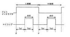
このような原子吸光分光光度計10では、次のようにして試料の吸光度を求める。まず、光源としてHCランプ11のみを用いる場合について説明する(以下、この場合をNon-BGC-Double測定モードと呼ぶ)。図3に、この場合におけるHCランプ11の点滅の様子を示す。フォトインタラプタ213は、サンプル光Lsがセクタミラー21を通過する期間(S期間)にはHレベルを出力し、リファレンス光Lrがセクタミラー21で反射される期間(R期間)にはLレベルを出力する。HCランプ11は、S期間とR期間が切り替わるとき、つまりフォトインタラプタ213の検知信号が変化する変化点Pから第1の所定時間Ta1を経過したときを始点として第2の所定時間Ta2だけ点灯し、それ以外の期間は消灯する。
In such an
このときの吸光度AHは、次の式で定義される。
AH=−log10TH
TH=(HS’×HR0’)/(HR’×HS0’)
この式に、下記記号に対応する値を代入することにより、試料の吸光度を求めることができる。
HS:S期間のHCランプ点灯中に取得されたサンプリングデータの平均値。
DKS:S期間のHCランプ消灯中に取得されたサンプリングデータの平均値。
HR:R期間のHCランプ点灯中に取得されたサンプリングデータの平均値。
DKR:R期間のHCランプ消灯中に取得されたサンプリングデータの平均値。
HS’=HS−DKS
HR’=HR−DKR
HS0’:試料が存在しない、つまり試料の原子化が行われていないときに予め取得されたHS’。
HR0’:試料が存在しない、つまり試料の原子化が行われていないときに予め取得されたHR’。
Absorbance A H in this case is defined by the following equation.
A H = -log 10 T H
T H = (H S '× H R0 ') / (H R '× H S0 ')
By substituting values corresponding to the following symbols into this equation, the absorbance of the sample can be obtained.
H S : Average value of sampling data acquired while the HC lamp is on during the S period.
DK S : Average value of sampling data acquired while the HC lamp is off during the S period.
H R : Average value of sampling data acquired while the HC lamp is on during the R period.
DK R : Average value of sampling data acquired while the HC lamp is turned off during the R period.
H S '= H S -DK S
H R '= H R -DK R
H S0 ': sample does not exist, that has been previously obtained H S while the atomization of the sample is not performed'.
H R0 ′: H R ′ acquired in advance when the sample does not exist, that is, when the sample is not atomized.
次に、光源としてHCランプ11とともにD2ランプ12も用いて、バックグラウンド補正を行う場合について説明する(以下、この場合をBGC-D2-Double測定モードと呼ぶ)。図4に、この場合におけるHCランプ11及びD2ランプ12の点滅の様子を示す。フォトインタラプタ213は、上記Non-BGC-Double測定モードと同様に、S期間にはHレベルを出力し、R期間にはLレベルを出力する。HCランプ11は、フォトインタラプタ213の検知信号の変化点Pから第3の所定時間Tb1を経過したときを始点として第4の所定時間Tb2だけ点灯し、それ以外の期間は消灯する。D2ランプ12は、検知信号の変化点Pから第5の所定時間Tc1を経過したときを始点として第6の所定時間Tc2だけ点灯し、それ以外の期間は消灯する。なお、HCランプ11とD2ランプ12の点灯は重ならないように設定されている。
Next, a case where background correction is performed using the
このときの吸光度ABGCは、次の式で定義される。
ABGC=−log10TBGC
TBGC=(HS’×HR0’×DR’×DS0’)/(HR’×HS0’×DS’×DR0’)
この式に、上記Non-BGC-Double測定モードでの吸光度を求める際に用いた記号に対応する値及び下記記号に対応する値を代入することにより、D2ランプ12によりバックグラウンド補正された試料の吸光度を求めることができる。
DS:S期間のD2ランプ点灯中に取得されたサンプリングデータの平均値。
DR:R期間のD2ランプ点灯中に取得されたサンプリングデータの平均値。
DS’=DS−DKS
DR’=DR−DKR
DS0’:試料が存在しない、つまり試料の原子化が行われていないときに予め取得されたDS’。
DR0’:試料が存在しない、つまり試料の原子化が行われていないときに予め取得されたDR’。
The absorbance A BGC at this time is defined by the following equation.
A BGC = -log 10 T BGC
T BGC = (H S ′ × H R 0 ′ × D R ′ × D S0 ′) / (H R ′ × H S0 ′ × D S ′ × D R0 ′)
By substituting the value corresponding to the symbol used to determine the absorbance in the Non-BGC-Double measurement mode and the value corresponding to the following symbol into this equation, the background corrected by the
D S : Average value of sampling data acquired while the D2 lamp is lit during the S period.
D R : Average value of sampling data acquired while the D2 lamp is lit during the R period.
D S '= D S -DK S
D R '= D R -DK R
D S0 ': sample does not exist, that has been previously obtained D S while the atomization of the sample is not performed'.
D R0 ′: D R ′ acquired in advance when the sample does not exist, that is, when the sample is not atomized.
一般に、セクタミラー21を回転させるモータ22は、構成を簡単にしてコストを抑え、かつ、回転音を極力小さくするなどのために、交流モータが使用され、商用交流電源で駆動されることが多い。この場合、交流モータの回転数は、交流電源の電源周波数に比例し、セクタミラーの回転数も交流電源の電源周波数に比例する。また、上記S期間及びR期間の長さはセクタミラー21の回転数に反比例する。従って、S期間及びR期間の長さは交流電源の電源周波数に反比例することになる。
In general, the
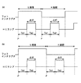
図5に、電源周波数が60Hzの場合(a)と50Hzの場合(b)のNon-BGC-Double測定モードでのHCランプ11の点滅の様子を示す。S期間及びR期間の長さは、上記理由により、電源周波数が60Hzの場合の方が短くなる。HCランプ11は、いずれの場合も、フォトインタラプタ213の検知信号の変化点Pから第1の所定時間Ta1を経過したときを始点として第2の所定時間Ta2だけ点灯するように設定されているため、第1及び第2の所定時間Ta1、Ta2は、点滅間隔が短い60Hzの場合に合わせて定められている。
FIG. 5 shows how the
しかし、このような設定では、S期間及びR期間が長い50Hzの場合、つまり交流電源の電源周波数が低い場合には、単位時間あたりのランプの点灯回数が減る。一方、点灯時間である第2の所定時間Ta2は一定値に定められているため、電源周波数が低い場合には、単位時間あたりの総点灯時間が短くなり、点灯中に取得されるサンプリングデータの数が少なくなる。これにより、サンプリングデータの統計誤差が大きくなって、元素の検出下限性能が低下する。この問題は、BGC-D2-Double測定モードでも同様に発生する。 However, in such a setting, when the S period and the R period are long 50 Hz, that is, when the power supply frequency of the AC power supply is low, the number of times the lamp is lit is reduced. On the other hand, since the second predetermined time Ta2, which is the lighting time, is set to a constant value, when the power supply frequency is low, the total lighting time per unit time is shortened, and the sampling data acquired during lighting is reduced. The number decreases. Thereby, the statistical error of sampling data becomes large and the detection lower limit performance of an element falls. This problem also occurs in the BGC-D2-Double measurement mode.
本発明は以上のような課題を解決するために成されたものであり、その目的は、交流電源の電源周波数に依存せずに、常に検出下限性能が最適化された状態で測定データを取得することができる原子吸光分光光度計を提供することである。 The present invention has been made to solve the above-described problems, and its purpose is not to depend on the power supply frequency of the AC power supply, but to always acquire measurement data with the detection lower limit performance optimized. It is to provide an atomic absorption spectrophotometer that can.
上記課題を解決するために成された本発明に係る原子吸光分光光度計は、
a)光源から発せられる光を2方向に分割し、一方の光は試料の原子化部を通過させ、他方の光は該原子化部以外の空間を通過させた後、各光を、交流モータにより回転するセクタミラーに導入し分光器へ交互に入射させ、該分光器で分光された光を検出器に入射させる光学系と、
b)前記セクタミラーの回転に同期して、前記光源を所定の点灯期間だけ点灯させる光源制御手段と、
c)前記セクタミラーの回転に同期して、前記検出器から出力される検出信号のサンプリングデータを所定の抽出期間に抽出するサンプリングデータ抽出手段と、
を備える原子吸光分光光度計であって、
d)前記点灯期間及び抽出期間の設定値を、前記交流モータを駆動させる交流電源の電源周波数に対応させて複数記憶するための記憶手段と、
e)交流電源の電源周波数を識別する周波数識別手段と、
f)前記記憶手段から、前記周波数識別手段により識別された電源周波数に対応した設定値を読み取り、該設定値に基づいて前記光源の点灯期間及びサンプリングデータの抽出期間を設定する点灯抽出期間設定手段と、
を備えることを特徴とする。
An atomic absorption spectrophotometer according to the present invention made to solve the above problems,
a) The light emitted from the light source is divided into two directions, one light passes through the atomized portion of the sample, and the other light passes through a space other than the atomized portion, and then each light is converted into an AC motor. An optical system for introducing the light into the sector mirror that is rotated by the light source and alternately entering the spectroscope, and allowing the light dispersed by the spectroscope to enter the detector;
b) Light source control means for lighting the light source for a predetermined lighting period in synchronization with the rotation of the sector mirror;
c) sampling data extraction means for extracting sampling data of the detection signal output from the detector in a predetermined extraction period in synchronization with the rotation of the sector mirror;
An atomic absorption spectrophotometer comprising:
d) storage means for storing a plurality of set values of the lighting period and the extraction period in correspondence with a power supply frequency of an AC power source that drives the AC motor;
e) a frequency identification means for identifying the power supply frequency of the AC power supply;
f) A lighting extraction period setting unit that reads a setting value corresponding to the power supply frequency identified by the frequency identification unit from the storage unit, and sets a lighting period of the light source and an extraction period of sampling data based on the setting value. When,
It is characterized by providing.
ここでいう光源制御手段は、光源自体を点灯、消灯させるものであっても、光源から発せられる光をシャッタ等で周期的に遮断するものであってもよい。 The light source control means here may be one that turns on and off the light source itself, or one that periodically blocks light emitted from the light source with a shutter or the like.
本発明に係る原子吸光分光光度計によれば、予め記憶手段に記憶された複数の設定値のうちから電源周波数に対応した設定値が読み取られ、その設定値に基づいて光源の点灯期間及びサンプリングデータの抽出期間が設定されるため、電源周波数が異なっても、光源の点灯期間及びサンプリングデータの抽出期間を最適に設定することができる。つまり、交流電源の電源周波数に依存せずに、常に検出下限性能が最適化された状態で測定データを取得することができる。 According to the atomic absorption spectrophotometer according to the present invention, the setting value corresponding to the power supply frequency is read from the plurality of setting values stored in advance in the storage unit, and the lighting period of the light source and sampling are performed based on the setting value. Since the data extraction period is set, the lighting period of the light source and the sampling data extraction period can be optimally set even if the power supply frequency is different. That is, the measurement data can be obtained in a state where the detection lower limit performance is always optimized without depending on the power supply frequency of the AC power supply.
以下、本発明の一実施形態に係る原子吸光分光光度計について説明する。図6は本実施形態に係る原子吸光分光光度計110の概略構成図である。原子吸光分光光度計110は、図1に示した従来の原子吸光分光光度計10と同様の光学系を有し、ホロカソード(HC)ランプ11、重水素(D2)ランプ12、ハーフミラー13、原子化部18、セクタミラー61、交流モータ22、フォトインタラプタ613、分光器30、検出器36、制御部41を主な構成要素とする。交流モータ22は50Hz又は60Hzの商用交流電源により駆動する。分光器30は、入口スリット31、凹球面鏡32、34、平面回折格子33、出口スリット35から構成される。検出器36としては光電子増倍管等を用いることができる。
Hereinafter, an atomic absorption spectrophotometer according to an embodiment of the present invention will be described. FIG. 6 is a schematic configuration diagram of the
制御部41は、CPUやROM421(フラッシュメモリであってもよい)を始めとする各種電子回路(RAM、PC50との通信に用いられるシリアルインターフェースの制御回路など)を内蔵するマイコンチップ42と、マイコンチップ42に接続し各種ハードウェアの制御を行うプログラマブルロジックデバイス(PLD)43と、検出器36から出力される検出信号を増幅する増幅器45と、増幅された検出信号をデジタル信号に変換し、そのデジタル信号をPLD43に送るA/D変換器46と、PLD43の指示に従ってHCランプ11及びD2ランプ12を点灯させる光源駆動部47から構成される。
マイコンチップ42内のROM421には、マイコンCPU上で動作する制御プログラムが書き込まれている。光源の点灯期間及びサンプリングデータの抽出期間に関する最適設定値は、電源周波数(50Hz又は60Hz)及び測定モード(Non-BGC-Double測定モード又はBGC-D2-Double測定モード)に基づいて場合分けされており、マイコンチップ42上で動作する制御プログラムの内部変数として取り扱われる。以下、マイコンチップ42と表現した場合は、上記制御プログラム機能をチップの一部として持つものとする。
The
A control program that operates on the microcomputer CPU is written in the
図7に、本実施形態におけるセクタミラー61の正面図(a)及び上面図(b)を示す。セクタミラー61は、中心角が90°の扇形の2枚のミラー611が軸部612に対して対称に取り付けられたものである。軸612には交流モータ22が接続されており、セクタミラー61は交流モータ22によって軸部612を中心に回転する。
軸部612には、扇形の2枚のタイミング・プレート615が、正面から見るとミラー611にほぼ重なる位置に取り付けられている。タイミング・プレート615の中心角はミラー611よりも小さい。
タイミング・プレート615の回転軌道上には、その軌道を挟むように、2つのフォトインタラプタ613が90°の角度をなして配置されている。各フォトインタラプタ613はその位置にタイミング・プレート615が存在するときにはHレベルを、タイミング・プレート615が存在しないときにはLレベルを検知信号として出力する。
ミラー611とタイミング・プレート615の中心角の角度差は、回転するミラー611の縁が、セクタミラー61での光源光の領域Aの端から端に移動するときのミラー611の回転角度と同じにする。これにより、一方のフォトインタラプタ613(図7(a)では右側のフォトインタラプタ)にはミラー611が領域Aから完全に外れているときのみHレベルを出力させ、他方のフォトインタラプタ613(図7(a)では左側のフォトインタラプタ)にはミラー611が領域Aの全域を覆っているときのみHレベルを出力させることができる。
FIG. 7 shows a front view (a) and a top view (b) of the
Two fan-shaped
On the rotational trajectory of the
The angle difference between the central angles of the
光源の点灯期間及びサンプリングデータの抽出期間に関する設定値について図8を用いて説明する。この例では、Non-BGC-Double測定モードにてHCランプ11のみを点滅させており、設定値として第1、第2、第3の所定時間Td1、Td2、Td3が定められている。ここでの光源の点灯及びサンプリングデータの抽出は次のように行われる。まず、フォトインタラプタ613の検知信号の変化点P(本実施形態では、2つあるフォトインタラプタのうち、どちらか一方がLレベルからHレベルに変化した時点から、もう一方がLレベルからHレベルに変化する時点までの期間を、S期間、またはR期間とし、それら期間が始まる時点を、変化点Pとする)から第1の所定時間Td1が経過し、さらに第2の所定時間Td2が経過すると、その時点を始点として第3の所定時間Td3だけサンプリングデータが抽出される。このデータは光源が消灯しているときのものである。次に、その抽出の終了と同時にHCランプ11が点灯し、さらにそこから第2の所定時間Td2だけ経過した時点を始点として第3の所定時間Td3だけサンプリングデータが抽出される。このデータは光源が点灯しているときのものである。その抽出の終了と同時にHCランプ11は消灯する。なお、この例は一例であって、光源の点灯期間及びサンプリングデータの抽出期間に関する設定値は上記以外にも様々な方法で定めることができる。
The setting values relating to the lighting period of the light source and the sampling data extraction period will be described with reference to FIG. In this example, only the
以下、本実施形態に係る原子吸光分光光度計110の動作について説明する。原子吸光分光光度計110では、装置電源投入時に、マイコンチップ42の指示により、交流モータ22を駆動してセクタミラー61を一時的に回転させる。その回転に伴ってフォトインタラプタ613からHレベルとLレベルの信号が周期的に出力され、その信号がPLD43を介してマイコンチップ42に到達する。マイコンチップ42は、受信した信号に基づいてS期間及びR期間の長さを判断し、商用交流電源の電源周波数(50Hz/60Hz)を識別する。その後、ユーザによりPC50又は図示しない入力装置より測定モードが選択されると、マイコンチップ42は、制御プログラム内部変数として記憶保持している2種類(50Hz用、または60Hz用)の光源点灯期間及びサンプリングデータ抽出期間の中から、識別した電源周波数のものを選択し、点灯期間をハードウェア(PLD43)に設定する。
Hereinafter, the operation of the
測定中においても、セクタミラー61の回転に伴ってフォトインタラプタ613から周期的に出力される検知信号がPLD43に伝達される。PLD43は、受信した検知信号の変化点P及びマイコンチップ42から設定された光源の点灯期間に関する設定値に基づいて、光源駆動部47に光源の点灯及び消灯を指示する。光源駆動部47は、その指示に従ってHCランプ11及びD2ランプ12に電流を供給し、それらを点灯及び消灯させる。
Even during the measurement, a detection signal periodically output from the
HCランプ11及びD2ランプ12から発せられた光は、ハーフミラー13、セクタミラー61、分光器30等を経由して検出器36に入射する。検出器36では、入射した光が光電変換され、光強度に応じた検出信号が出力される。その検出信号は、増幅器45で増幅され、A/D変換器46で所定のサンプリング間隔(例えば10μs)でデジタル信号に変換されて、そのサンプリングデータがPLD43を介してマイコンチップ42に送られる。
Light emitted from the
マイコンチップ42は、フォトインタラプタ613の検知信号の変化点P、及び電源周波数と測定モードから決定したサンプリングデータの抽出期間に関する設定値に基づいて、受信したサンプリングデータの中から特定の期間のデータのみを抽出し、そのデータを所定のデータメモリに記録する。このようにして得られたサンプリングデータを用いることにより試料の吸光度を算出することができる。
The
本実施例に係る原子吸光分光光度計110では、光源の点灯期間に関するデフォルトの設定値は上記のとおり、マイコンチップ42の制御プログラム内部変数として記憶されているが、PC50から送られる制御コマンドによって上記内部変数を書き換えることにより、光源の点灯期間を一時的に変更することが可能である。また、サンプリングデータの抽出期間も同様に、上記内部変数を書き換えることによって変更することが可能である。このような書き換えの作業は、装置から回路基板を取り出さなくても行えるものであるため、各設定値を頻繁に変更することが容易であり、各設定値の最適値を探索する際などに有用である。なお、各設定値の最適値を探索する作業は、通常、ユーザが行うのではなく、装置の開発者が行う。
In the
以下、各設定値の最適化の手順の一例を図9〜12を用いて説明する。この例では、Non-BGC-Double測定モードにてHCランプ11のみを点滅させることとし、HCランプ11はCu(吸光波長324.7nm)、HCランプ11の光量を決めるランプ電流値は8mA、サンプリング間隔は10μsとする。光源の点灯期間及びサンプリングデータの抽出期間に関する設定値は、以下の時間T1、T2、T3として定める。
T1:第1切り捨て時間(×10μs)
T2:第2切り捨て時間(×10μs)
T3:データ取得対象時間(×10μs)
Hereinafter, an example of a procedure for optimizing each set value will be described with reference to FIGS. In this example, only the
T1: First round-off time (× 10μs)
T2: Second truncation time (× 10μs)
T3: Data acquisition target time (× 10μs)
上記T1〜T3に基づいて、サンプリングデータの抽出期間は次のようにして決まる。図9に示すように、フォトインタラプタ613の検知信号の変化点Pから第1切り捨て時間T1経過後に、データ取得対象時間T3が始まる。データ取得対象時間T3は、S期間及びR期間におけるサンプリングデータの取得対象時間であり、その前半の1/2が消灯時データ取得対象時間T3A、後半の1/2が点灯時データ取得対象時間T3Bである。ただし、光源の立ち上がり時の光量は不安定であるため、サンプリングデータは、点灯時データ取得対象時間T3Bの開始時から第2切り捨て時間T2の間は抽出せず、その後の点灯時データ取得対象時間T3Bにのみ抽出する。なお、データ処理の対称性の都合上、消灯時データ取得対象時間T3Aにおいても、サンプリングデータは、その開始時から第2切り捨て時間T2の間は抽出せず、その後の消灯時データ取得対象時間T3Aにのみ抽出する。
Based on T1 to T3, the sampling data extraction period is determined as follows. As shown in FIG. 9, the data acquisition target time T3 starts after the first truncation time T1 has elapsed from the change point P of the detection signal of the
このようなT1〜T3は、ベースライン測定(試料を何も導入してない状態での測定)時の吸光度の標準偏差(SD値)が最小になるように最適化する。このSD値は、5秒間の吸光度の測定を7回行って各測定での吸光度の平均値の標準偏差を求めるという作業を10回繰り返し、それにより得られる10個の標準偏差を平均した値として定義する。
Such T1 to T3 are optimized so that the standard deviation (SD value) of the absorbance at the time of baseline measurement (measurement in a state where no sample is introduced) is minimized. This SD value is obtained by repeating the work of measuring the absorbance for 5 seconds 7 times and obtaining the standard deviation of the average value of absorbance in each
図10に、電源周波数が60Hz(S期間及びR期間が833×10μs)の場合にT2及びT3を固定し(T2=0μs、T3=460×10μs)、T1を0〜360×10μsの範囲で変化させたときの吸光度のSD値の変化の様子を示す。この図の横軸はT1とT3を足し合わせた時間を表す。この図より、T1とT3を足し合わせた時間が最小値(460×10μs)のとき、つまりT1=0μsのときであっても、吸光度のSD値は最小一定値を取ることが分かる。従って、T1の最適値を0μsとした。なお、T1とT3を足し合わせた時間が700×10μsを過ぎるあたりから、吸光度のSD値が急激に上昇しているが、これは、図9に示すように、セクタミラー61に到達する光が、設計上、セクタミラー61の回転角の12.7°に対応する幅を有しており、その光が上記時間を過ぎるあたりでミラー211の端部に差し掛かるために生じると解釈することができる。
In FIG. 10, when the power supply frequency is 60 Hz (S period and R period are 833 × 10 μs), T2 and T3 are fixed (T2 = 0 μs, T3 = 460 × 10 μs), and T1 is in the range of 0 to 360 × 10 μs. The state of change in the SD value of absorbance when changed is shown. The horizontal axis of this figure represents the time when T1 and T3 are added. From this figure, it can be seen that even when the time when T1 and T3 are added is the minimum value (460 × 10 μs), that is, when T1 = 0 μs, the SD value of absorbance takes the minimum constant value. Therefore, the optimum value of T1 is set to 0 μs. Note that the absorbance SD value has increased rapidly since the time when T1 and T3 are added exceeds 700 × 10 μs. This is because the light reaching the
図11に、T1及びT2を固定し(T1=0μs、T2=0μs)、T3を460〜780×10μsの範囲で変化させたときの吸光度のSD値の変化の様子を示す。この図より、T3=600×10μsのときに吸光度のSD値は最小値を取ることが分かる。従って、T3の最適値を600×10μsとした。 FIG. 11 shows how the absorbance SD value changes when T1 and T2 are fixed (T1 = 0 μs, T2 = 0 μs) and T3 is changed in the range of 460 to 780 × 10 μs. From this figure, it is understood that the SD value of absorbance takes the minimum value when T3 = 600 × 10 μs. Therefore, the optimum value of T3 is set to 600 × 10 μs.
図12に、T1及びT3を固定し(T1=0μs、T3=600×10μs)、T2を0〜90×10μsの範囲で変化させたときの吸光度のSD値の変化の様子を示す。この図より、T2=30×10μsのときに吸光度のSD値は最小値を取ることが分かる。従って、T2の最適値を30×10μsとした。なお、このように測定範囲の両端でSD値が大きくなることは、T2が小さすぎる場合には光源の立ち上がり時の不安定な測定データを使うことになるために生じ、逆にT2が大きすぎる場合には演算に用いるサンプリングデータの数が少なく統計上の誤差が大きくなるために生じると解釈することができる。 FIG. 12 shows how the absorbance SD value changes when T1 and T3 are fixed (T1 = 0 μs, T3 = 600 × 10 μs) and T2 is changed in the range of 0 to 90 × 10 μs. From this figure, it can be seen that the SD value of absorbance takes the minimum value when T2 = 30 × 10 μs. Therefore, the optimum value of T2 is set to 30 × 10 μs. Note that the SD value increases at both ends of the measurement range as described above, because when T2 is too small, unstable measurement data at the start of the light source is used, and conversely, T2 is too large. In some cases, it can be interpreted that this occurs because the number of sampling data used in the calculation is small and the statistical error is large.
以上をまとめると、本測定では、吸光度のSD値が最小になるときのT1〜T3は、T1=0μs、T2=30×10μs、T3=600×10μsであった。また、S期間及びR期間が833×10μsであることから、データ取得対象時間T3は、S期間及びR期間に対して600/833=0.72(72%)となっていた。 To summarize the above, in this measurement, T1 to T3 when the SD value of absorbance was minimized were T1 = 0 μs, T2 = 30 × 10 μs, and T3 = 600 × 10 μs. Further, since the S period and the R period are 833 × 10 μs, the data acquisition target time T3 is 600/833 = 0.72 (72%) with respect to the S period and the R period.
次に、電源周波数が50Hzの場合について検討する。この場合、S期間及びR期間は1000×10μsとなるため、上記結果を用いて、1000×0.72=720(×10μs)が最適なデータ取得対象時間T3となる。また、第2切り捨て時間T2は、セクタミラー61の回転数に寄らず、回路の電気特性にのみ依存すると考えられるため、60Hzのときと同様に、30×10μsを最適値とすることができる。つまり、この場合に吸光度のSD値が最小になるのは、第1切り捨て時間T1=0μs、第2切り捨て時間T2=30×10μs、データ取得対象時間T3=720×10μsのときである。
Next, consider the case where the power supply frequency is 50 Hz. In this case, since the S period and the R period are 1000 × 10 μs, 1000 × 0.72 = 720 (× 10 μs) is the optimum data acquisition target time T3 using the above result. In addition, since the second truncation time T2 is considered to depend only on the electrical characteristics of the circuit without depending on the rotational speed of the
さらに、BGC-D2-Double測定モードの場合について検討する。この場合、図13に示すように、フォトインタラプタ613の検知信号の変化点Pから第1切り捨て時間T1経過後に、第2のデータ取得対象時間T4が始まる。第2のデータ取得対象時間T4のうち、初めの1/4の時間はHCランプ消灯時データ取得対象時間T4Aであり、次の1/4の時間はHCランプ点灯時データ取得対象時間T4Bであり、その次の1/4の時間はD2ランプ消灯時データ取得対象時間T4Cであり、最後の1/4の時間はD2ランプ点灯時データ取得対象時間T4Dである。サンプリングデータは、上記Non-BGC-Double測定モードと同様に、T4A〜T4Dの各開始時から第2切り捨て時間T2の間は抽出されない。
Further, consider the case of BGC-D2-Double measurement mode. In this case, as shown in FIG. 13, the second data acquisition target time T4 starts after the first truncation time T1 has elapsed from the change point P of the detection signal of the
上記Non-BGC-Double測定モードにて得られた結果はここでも適用することが可能であり、第1切り捨て時間T1、第2切り捨て時間T2は上記と同じ値(T1=0μs、T2=30×10μs)が最適値となる。第2のデータ取得対象時間T4は、電源周波数が60Hzの場合は、S期間及びR期間が833×10μsであるため、833×0.72=600(×10μs)が最適値となる。電源周波数が50Hzの場合は、S期間及びR期間が1000×10μsであるため、1000×0.72=720(×10μs)が最適値となる。 The results obtained in the above Non-BGC-Double measurement mode can be applied here, and the first truncation time T1 and the second truncation time T2 are the same values as above (T1 = 0 μs, T2 = 30 × 10μs) is the optimum value. The second data acquisition target time T4 is 833 × 0.72 = 600 (× 10 μs) because the S period and the R period are 833 × 10 μs when the power supply frequency is 60 Hz. When the power supply frequency is 50 Hz, since the S period and the R period are 1000 × 10 μs, 1000 × 0.72 = 720 (× 10 μs) is the optimum value.
こうして求めた各値を、電源周波数及び測定モードに対応させて、マイコンチップ42の制御プログラム内部変数のデフォルト値として記憶保持しておくことにより、前述のような最適な測定を行うことができる。
Each value obtained in this way is stored and held as a default value of a control program internal variable of the
上記実施形態は本発明の一例であり、本発明の趣旨の範囲で適宜変更が許容される。例えば、光源を周期的に点灯及び消灯させる代わりに、光源から発せられる光をシャッタ等を用いて周期的に遮断することにより、光源を点滅させてもよい。サンプル光Ls及びリファレンス光Lrがセクタミラーに到達する位置は、光源の点灯期間やサンプリングデータの抽出時間の設定値を適切に定めておけば、図2に示した領域Aの位置でなくても構わない。フォトインタラプタは1つであってもよく、また、セクタミラーの回転軌道上に配置してもよい。設定値を記憶する記憶手段は、マイコンチップ外部のメモリ等であってもよい。 The above embodiment is an example of the present invention, and appropriate modifications are allowed within the scope of the present invention. For example, instead of periodically turning on and off the light source, the light source may be blinked by periodically blocking light emitted from the light source using a shutter or the like. The position at which the sample light Ls and the reference light Lr reach the sector mirror is not limited to the position of the region A shown in FIG. 2 as long as the light source lighting period and sampling data extraction time are set appropriately. I do not care. The number of photo interrupters may be one, and it may be arranged on the rotation trajectory of the sector mirror. The storage means for storing the set value may be a memory outside the microcomputer chip.
10、110…原子吸光分光光度計
11…HCランプ
12…D2ランプ
13…ハーフミラー
18…原子化部
21、61…セクタミラー
211、611…ミラー
212、612…軸部
213、613…フォトインタラプタ
22…モータ
30…分光器
31…入口スリット
32、34…凹球面鏡
33…平面回折格子
35…出口スリット
36…検出器
40、41…制御部
42…マイコンチップ
421…ROM
43…プログラマブルロジックデバイス(PLD)
45…増幅器
46…A/D変換器
47…光源駆動部
50…PC
615…タイミング・プレート
Lr…リファレンス光
Ls…サンプル光
DESCRIPTION OF
43. Programmable logic device (PLD)
45 ...
615 ... Timing plate Lr ... Reference light Ls ... Sample light
Claims (3)
b)前記セクタミラーの回転に同期して、前記光源を所定の点灯期間だけ点灯させる光源制御手段と、
c)前記セクタミラーの回転に同期して、前記検出器から出力される検出信号のサンプリングデータを所定の抽出期間に抽出するサンプリングデータ抽出手段と、
を備える原子吸光分光光度計であって、
d)前記点灯期間及び抽出期間の設定値を、前記交流モータを駆動させる交流電源の電源周波数に対応させて複数記憶するための記憶手段と、
e)交流電源の電源周波数を識別する周波数識別手段と、
f)前記記憶手段から、前記周波数識別手段により識別された電源周波数に対応した設定値を読み取り、該設定値に基づいて前記光源の点灯期間及びサンプリングデータの抽出期間を設定する点灯抽出期間設定手段と、
を備えることを特徴とする原子吸光分光光度計。 a) The light emitted from the light source is divided into two directions, one light passes through the atomized portion of the sample, and the other light passes through a space other than the atomized portion, and then each light is converted into an AC motor. An optical system for introducing the light into the sector mirror that is rotated by the light source and alternately entering the spectroscope, and allowing the light dispersed by the spectroscope to enter the detector;
b) Light source control means for lighting the light source for a predetermined lighting period in synchronization with the rotation of the sector mirror;
c) sampling data extraction means for extracting sampling data of the detection signal output from the detector in a predetermined extraction period in synchronization with the rotation of the sector mirror;
An atomic absorption spectrophotometer comprising:
d) storage means for storing a plurality of set values of the lighting period and the extraction period in correspondence with a power supply frequency of an AC power source that drives the AC motor;
e) a frequency identification means for identifying the power supply frequency of the AC power supply;
f) A lighting extraction period setting unit that reads a setting value corresponding to the power supply frequency identified by the frequency identification unit from the storage unit, and sets a lighting period of the light source and an extraction period of sampling data based on the setting value. When,
An atomic absorption spectrophotometer comprising:
Priority Applications (3)
| Application Number | Priority Date | Filing Date | Title |
|---|---|---|---|
| JP2008262414A JP5056712B2 (en) | 2008-10-09 | 2008-10-09 | Atomic absorption spectrophotometer |
| CN2009102046085A CN101718685B (en) | 2008-10-09 | 2009-09-29 | Atomic absorption spectrophotometer |
| US12/574,213 US8107072B2 (en) | 2008-10-09 | 2009-10-06 | Atomic absorption spectrophotometer |
Applications Claiming Priority (1)
| Application Number | Priority Date | Filing Date | Title |
|---|---|---|---|
| JP2008262414A JP5056712B2 (en) | 2008-10-09 | 2008-10-09 | Atomic absorption spectrophotometer |
Publications (2)
| Publication Number | Publication Date |
|---|---|
| JP2010091446A true JP2010091446A (en) | 2010-04-22 |
| JP5056712B2 JP5056712B2 (en) | 2012-10-24 |
Family
ID=42098569
Family Applications (1)
| Application Number | Title | Priority Date | Filing Date |
|---|---|---|---|
| JP2008262414A Active JP5056712B2 (en) | 2008-10-09 | 2008-10-09 | Atomic absorption spectrophotometer |
Country Status (3)
| Country | Link |
|---|---|
| US (1) | US8107072B2 (en) |
| JP (1) | JP5056712B2 (en) |
| CN (1) | CN101718685B (en) |
Cited By (2)
| Publication number | Priority date | Publication date | Assignee | Title |
|---|---|---|---|---|
| JP2012026830A (en) * | 2010-07-22 | 2012-02-09 | Shimadzu Corp | Gas concentration measurement instrument |
| JP2013011473A (en) * | 2011-06-28 | 2013-01-17 | Shimadzu Corp | Spectrophotometer |
Families Citing this family (1)
| Publication number | Priority date | Publication date | Assignee | Title |
|---|---|---|---|---|
| WO2015112775A1 (en) * | 2014-01-22 | 2015-07-30 | Swift Control Systems, Inc. | A smart mirror mount device |
Citations (4)
| Publication number | Priority date | Publication date | Assignee | Title |
|---|---|---|---|---|
| JPH09257703A (en) * | 1996-03-26 | 1997-10-03 | Hitachi Ltd | Atomic absorption spectrophotometer |
| JPH10325793A (en) * | 1997-05-23 | 1998-12-08 | Shimadzu Corp | Atomic absorption photometer |
| JP2002081991A (en) * | 2000-09-08 | 2002-03-22 | Shimadzu Corp | Optical analyzer |
| JP2003014631A (en) * | 2001-07-03 | 2003-01-15 | Shimadzu Corp | Atomic absorption spectrophotometer |
Family Cites Families (6)
| Publication number | Priority date | Publication date | Assignee | Title |
|---|---|---|---|---|
| DE2303533C2 (en) * | 1973-01-25 | 1984-03-08 | The Perkin-Elmer Corp., 06856 Norwalk, Conn. | Atomic absorption spectrophotometer |
| US4168910A (en) * | 1978-04-27 | 1979-09-25 | The Perkin-Elmer Corporation | Optical beam-switching chopper |
| EP0027148A1 (en) * | 1979-10-10 | 1981-04-22 | Siemens Aktiengesellschaft | Optoelectronic device |
| US4332470A (en) * | 1980-03-07 | 1982-06-01 | The Perkin-Elmer Corporation | Spectrophotometer system having power line synchronization |
| GB9210674D0 (en) * | 1992-05-19 | 1992-07-01 | Gersan Ets | Method and apparatus for examining an object |
| CN2708302Y (en) * | 2004-02-12 | 2005-07-06 | 北京天方辰星科技有限公司 | Double-lamp and double-atomizer integrated atomic absorption spectrometer |
-
2008
- 2008-10-09 JP JP2008262414A patent/JP5056712B2/en active Active
-
2009
- 2009-09-29 CN CN2009102046085A patent/CN101718685B/en not_active Expired - Fee Related
- 2009-10-06 US US12/574,213 patent/US8107072B2/en active Active
Patent Citations (4)
| Publication number | Priority date | Publication date | Assignee | Title |
|---|---|---|---|---|
| JPH09257703A (en) * | 1996-03-26 | 1997-10-03 | Hitachi Ltd | Atomic absorption spectrophotometer |
| JPH10325793A (en) * | 1997-05-23 | 1998-12-08 | Shimadzu Corp | Atomic absorption photometer |
| JP2002081991A (en) * | 2000-09-08 | 2002-03-22 | Shimadzu Corp | Optical analyzer |
| JP2003014631A (en) * | 2001-07-03 | 2003-01-15 | Shimadzu Corp | Atomic absorption spectrophotometer |
Cited By (2)
| Publication number | Priority date | Publication date | Assignee | Title |
|---|---|---|---|---|
| JP2012026830A (en) * | 2010-07-22 | 2012-02-09 | Shimadzu Corp | Gas concentration measurement instrument |
| JP2013011473A (en) * | 2011-06-28 | 2013-01-17 | Shimadzu Corp | Spectrophotometer |
Also Published As
| Publication number | Publication date |
|---|---|
| CN101718685B (en) | 2012-11-07 |
| CN101718685A (en) | 2010-06-02 |
| JP5056712B2 (en) | 2012-10-24 |
| US20100091277A1 (en) | 2010-04-15 |
| US8107072B2 (en) | 2012-01-31 |
Similar Documents
| Publication | Publication Date | Title |
|---|---|---|
| US9752933B2 (en) | Optical emission system including dichroic beam combiner | |
| JP5056712B2 (en) | Atomic absorption spectrophotometer | |
| JP5008831B2 (en) | Laser apparatus, laser apparatus control apparatus, laser apparatus control method, laser apparatus wavelength switching method, and laser apparatus control data | |
| JP2007218787A (en) | Wavelength calibration method and device | |
| US20230213386A1 (en) | Imaging device with spectrometer and methods for use therewith | |
| JP7253728B2 (en) | Human detection system and program | |
| JP5875741B1 (en) | Gas measuring device and measuring method | |
| US20170195586A1 (en) | User device | |
| WO2014030475A1 (en) | Spectrophotometer | |
| JP6201547B2 (en) | Spectrometer wavelength calibration method | |
| JP2007064632A (en) | Spectrophotometer | |
| EP3168600A1 (en) | Biological component information measurement device | |
| JP2010139299A (en) | Gas sensor | |
| US9500520B2 (en) | Optical measurement apparatus | |
| JP4660696B2 (en) | Reflection characteristic measuring device | |
| WO2014196363A1 (en) | Spectroscopic system and method | |
| JP2010286291A (en) | Infrared spectroscope and infrared spectral measuring device | |
| US8953160B2 (en) | Systems having a reflected light sensor and methods of use | |
| EP3184977A1 (en) | User device | |
| JP2005115060A (en) | External flash device | |
| JP2019113479A (en) | Analyzer and warming-up determination method | |
| JP2006078409A (en) | Spectrophotometer and spectroscopy | |
| JP2005147811A (en) | Spectrophotometer | |
| JPH10185686A (en) | Spectrophotometer | |
| JP2013011473A (en) | Spectrophotometer |
Legal Events
| Date | Code | Title | Description |
|---|---|---|---|
| A621 | Written request for application examination |
Free format text: JAPANESE INTERMEDIATE CODE: A621 Effective date: 20110228 |
|
| RD02 | Notification of acceptance of power of attorney |
Free format text: JAPANESE INTERMEDIATE CODE: A7422 Effective date: 20110228 |
|
| A977 | Report on retrieval |
Free format text: JAPANESE INTERMEDIATE CODE: A971007 Effective date: 20120515 |
|
| TRDD | Decision of grant or rejection written | ||
| A01 | Written decision to grant a patent or to grant a registration (utility model) |
Free format text: JAPANESE INTERMEDIATE CODE: A01 Effective date: 20120703 |
|
| A01 | Written decision to grant a patent or to grant a registration (utility model) |
Free format text: JAPANESE INTERMEDIATE CODE: A01 |
|
| A61 | First payment of annual fees (during grant procedure) |
Free format text: JAPANESE INTERMEDIATE CODE: A61 Effective date: 20120716 |
|
| FPAY | Renewal fee payment (event date is renewal date of database) |
Free format text: PAYMENT UNTIL: 20150810 Year of fee payment: 3 |
|
| R151 | Written notification of patent or utility model registration |
Ref document number: 5056712 Country of ref document: JP Free format text: JAPANESE INTERMEDIATE CODE: R151 |
|
| FPAY | Renewal fee payment (event date is renewal date of database) |
Free format text: PAYMENT UNTIL: 20150810 Year of fee payment: 3 |