JP2010062387A - Nonvolatile semiconductor storage device - Google Patents
Nonvolatile semiconductor storage device Download PDFInfo
- Publication number
- JP2010062387A JP2010062387A JP2008227418A JP2008227418A JP2010062387A JP 2010062387 A JP2010062387 A JP 2010062387A JP 2008227418 A JP2008227418 A JP 2008227418A JP 2008227418 A JP2008227418 A JP 2008227418A JP 2010062387 A JP2010062387 A JP 2010062387A
- Authority
- JP
- Japan
- Prior art keywords
- layer
- insulating film
- film
- low
- tunnel insulating
- Prior art date
- Legal status (The legal status is an assumption and is not a legal conclusion. Google has not performed a legal analysis and makes no representation as to the accuracy of the status listed.)
- Granted
Links
- 239000004065 semiconductor Substances 0.000 title claims abstract description 73
- 238000003860 storage Methods 0.000 title claims abstract description 29
- 230000005684 electric field Effects 0.000 claims abstract description 92
- 239000000758 substrate Substances 0.000 claims abstract description 56
- 239000000463 material Substances 0.000 claims abstract description 29
- 239000010410 layer Substances 0.000 claims description 611
- 229910052814 silicon oxide Inorganic materials 0.000 claims description 29
- VYPSYNLAJGMNEJ-UHFFFAOYSA-N Silicium dioxide Chemical compound O=[Si]=O VYPSYNLAJGMNEJ-UHFFFAOYSA-N 0.000 claims description 25
- 229910052735 hafnium Inorganic materials 0.000 claims description 10
- -1 lanthanum aluminate Chemical class 0.000 claims description 9
- 239000002356 single layer Substances 0.000 claims description 9
- MRELNEQAGSRDBK-UHFFFAOYSA-N lanthanum(3+);oxygen(2-) Chemical group [O-2].[O-2].[O-2].[La+3].[La+3] MRELNEQAGSRDBK-UHFFFAOYSA-N 0.000 claims description 8
- 229910052746 lanthanum Inorganic materials 0.000 claims description 6
- BPQQTUXANYXVAA-UHFFFAOYSA-N Orthosilicate Chemical compound [O-][Si]([O-])([O-])[O-] BPQQTUXANYXVAA-UHFFFAOYSA-N 0.000 claims description 5
- VBJZVLUMGGDVMO-UHFFFAOYSA-N hafnium atom Chemical group [Hf] VBJZVLUMGGDVMO-UHFFFAOYSA-N 0.000 claims description 5
- 241000588731 Hafnia Species 0.000 claims description 3
- PNEYBMLMFCGWSK-UHFFFAOYSA-N aluminium oxide Inorganic materials [O-2].[O-2].[O-2].[Al+3].[Al+3] PNEYBMLMFCGWSK-UHFFFAOYSA-N 0.000 claims description 3
- CJNBYAVZURUTKZ-UHFFFAOYSA-N hafnium(IV) oxide Inorganic materials O=[Hf]=O CJNBYAVZURUTKZ-UHFFFAOYSA-N 0.000 claims description 3
- FZLIPJUXYLNCLC-UHFFFAOYSA-N lanthanum atom Chemical group [La] FZLIPJUXYLNCLC-UHFFFAOYSA-N 0.000 claims description 3
- 229910052762 osmium Inorganic materials 0.000 claims description 3
- 229910052720 vanadium Inorganic materials 0.000 claims description 3
- 229910052804 chromium Inorganic materials 0.000 claims description 2
- 229910052748 manganese Inorganic materials 0.000 claims description 2
- 239000010408 film Substances 0.000 description 395
- 229910004298 SiO 2 Inorganic materials 0.000 description 110
- HQVNEWCFYHHQES-UHFFFAOYSA-N silicon nitride Chemical compound N12[Si]34N5[Si]62N3[Si]51N64 HQVNEWCFYHHQES-UHFFFAOYSA-N 0.000 description 46
- 229910052581 Si3N4 Inorganic materials 0.000 description 45
- 238000000034 method Methods 0.000 description 29
- 230000000694 effects Effects 0.000 description 18
- 230000004888 barrier function Effects 0.000 description 15
- 229910052710 silicon Inorganic materials 0.000 description 14
- 229910004129 HfSiO Inorganic materials 0.000 description 13
- 238000005229 chemical vapour deposition Methods 0.000 description 13
- 230000014759 maintenance of location Effects 0.000 description 13
- 229910018072 Al 2 O 3 Inorganic materials 0.000 description 12
- XUIMIQQOPSSXEZ-UHFFFAOYSA-N Silicon Chemical compound [Si] XUIMIQQOPSSXEZ-UHFFFAOYSA-N 0.000 description 12
- 239000010703 silicon Substances 0.000 description 12
- 229910021193 La 2 O 3 Inorganic materials 0.000 description 10
- 230000005641 tunneling Effects 0.000 description 10
- 229910021420 polycrystalline silicon Inorganic materials 0.000 description 9
- 238000002955 isolation Methods 0.000 description 8
- 238000004519 manufacturing process Methods 0.000 description 8
- 230000007547 defect Effects 0.000 description 7
- 238000010586 diagram Methods 0.000 description 6
- 229910003855 HfAlO Inorganic materials 0.000 description 5
- 238000004364 calculation method Methods 0.000 description 5
- 239000007789 gas Substances 0.000 description 5
- 238000001020 plasma etching Methods 0.000 description 5
- QGZKDVFQNNGYKY-UHFFFAOYSA-N Ammonia Chemical compound N QGZKDVFQNNGYKY-UHFFFAOYSA-N 0.000 description 4
- KRHYYFGTRYWZRS-UHFFFAOYSA-N Fluorane Chemical compound F KRHYYFGTRYWZRS-UHFFFAOYSA-N 0.000 description 4
- 230000006870 function Effects 0.000 description 4
- 230000003647 oxidation Effects 0.000 description 4
- 238000007254 oxidation reaction Methods 0.000 description 4
- 229910052760 oxygen Inorganic materials 0.000 description 4
- 239000000654 additive Substances 0.000 description 3
- 230000000996 additive effect Effects 0.000 description 3
- 238000000231 atomic layer deposition Methods 0.000 description 3
- QVGXLLKOCUKJST-UHFFFAOYSA-N atomic oxygen Chemical compound [O] QVGXLLKOCUKJST-UHFFFAOYSA-N 0.000 description 3
- 230000008859 change Effects 0.000 description 3
- 229910021419 crystalline silicon Inorganic materials 0.000 description 3
- 238000009792 diffusion process Methods 0.000 description 3
- 238000005530 etching Methods 0.000 description 3
- 239000012535 impurity Substances 0.000 description 3
- 239000011229 interlayer Substances 0.000 description 3
- 239000001301 oxygen Substances 0.000 description 3
- UFHFLCQGNIYNRP-UHFFFAOYSA-N Hydrogen Chemical compound [H][H] UFHFLCQGNIYNRP-UHFFFAOYSA-N 0.000 description 2
- 229910010413 TiO 2 Inorganic materials 0.000 description 2
- 229910021529 ammonia Inorganic materials 0.000 description 2
- 229910052785 arsenic Inorganic materials 0.000 description 2
- 230000008901 benefit Effects 0.000 description 2
- 230000015572 biosynthetic process Effects 0.000 description 2
- 238000002485 combustion reaction Methods 0.000 description 2
- 238000000151 deposition Methods 0.000 description 2
- 238000009826 distribution Methods 0.000 description 2
- 229910052739 hydrogen Inorganic materials 0.000 description 2
- 239000001257 hydrogen Substances 0.000 description 2
- 238000005468 ion implantation Methods 0.000 description 2
- 238000000608 laser ablation Methods 0.000 description 2
- 238000001451 molecular beam epitaxy Methods 0.000 description 2
- 229910052698 phosphorus Inorganic materials 0.000 description 2
- 230000008569 process Effects 0.000 description 2
- 229910052707 ruthenium Inorganic materials 0.000 description 2
- 238000004544 sputter deposition Methods 0.000 description 2
- 238000007740 vapor deposition Methods 0.000 description 2
- OKTJSMMVPCPJKN-UHFFFAOYSA-N Carbon Chemical compound [C] OKTJSMMVPCPJKN-UHFFFAOYSA-N 0.000 description 1
- 229910001218 Gallium arsenide Inorganic materials 0.000 description 1
- 229910004140 HfO Inorganic materials 0.000 description 1
- 206010021143 Hypoxia Diseases 0.000 description 1
- OAICVXFJPJFONN-UHFFFAOYSA-N Phosphorus Chemical compound [P] OAICVXFJPJFONN-UHFFFAOYSA-N 0.000 description 1
- 229910052782 aluminium Inorganic materials 0.000 description 1
- RQNWIZPPADIBDY-UHFFFAOYSA-N arsenic atom Chemical compound [As] RQNWIZPPADIBDY-UHFFFAOYSA-N 0.000 description 1
- 229910052799 carbon Inorganic materials 0.000 description 1
- 230000015556 catabolic process Effects 0.000 description 1
- 230000002950 deficient Effects 0.000 description 1
- BUMGIEFFCMBQDG-UHFFFAOYSA-N dichlorosilicon Chemical compound Cl[Si]Cl BUMGIEFFCMBQDG-UHFFFAOYSA-N 0.000 description 1
- 238000005516 engineering process Methods 0.000 description 1
- 230000004907 flux Effects 0.000 description 1
- 230000005524 hole trap Effects 0.000 description 1
- 238000010030 laminating Methods 0.000 description 1
- 239000011159 matrix material Substances 0.000 description 1
- 230000007246 mechanism Effects 0.000 description 1
- 229910052751 metal Inorganic materials 0.000 description 1
- 239000002184 metal Substances 0.000 description 1
- 229910044991 metal oxide Inorganic materials 0.000 description 1
- 238000012986 modification Methods 0.000 description 1
- 230000004048 modification Effects 0.000 description 1
- 229910021421 monocrystalline silicon Inorganic materials 0.000 description 1
- 150000004767 nitrides Chemical class 0.000 description 1
- 229910052757 nitrogen Inorganic materials 0.000 description 1
- BPUBBGLMJRNUCC-UHFFFAOYSA-N oxygen(2-);tantalum(5+) Chemical group [O-2].[O-2].[O-2].[O-2].[O-2].[Ta+5].[Ta+5] BPUBBGLMJRNUCC-UHFFFAOYSA-N 0.000 description 1
- 239000011574 phosphorus Substances 0.000 description 1
- 238000005498 polishing Methods 0.000 description 1
- 230000001737 promoting effect Effects 0.000 description 1
- 230000000717 retained effect Effects 0.000 description 1
- 239000000126 substance Substances 0.000 description 1
- 239000002344 surface layer Substances 0.000 description 1
- 229910001936 tantalum oxide Inorganic materials 0.000 description 1
- 229910052713 technetium Inorganic materials 0.000 description 1
- 239000010409 thin film Substances 0.000 description 1
- LXEXBJXDGVGRAR-UHFFFAOYSA-N trichloro(trichlorosilyl)silane Chemical compound Cl[Si](Cl)(Cl)[Si](Cl)(Cl)Cl LXEXBJXDGVGRAR-UHFFFAOYSA-N 0.000 description 1
- WQJQOUPTWCFRMM-UHFFFAOYSA-N tungsten disilicide Chemical compound [Si]#[W]#[Si] WQJQOUPTWCFRMM-UHFFFAOYSA-N 0.000 description 1
- 229910021342 tungsten silicide Inorganic materials 0.000 description 1
Images


Classifications
-
- H—ELECTRICITY
- H01—ELECTRIC ELEMENTS
- H01L—SEMICONDUCTOR DEVICES NOT COVERED BY CLASS H10
- H01L29/00—Semiconductor devices adapted for rectifying, amplifying, oscillating or switching, or capacitors or resistors with at least one potential-jump barrier or surface barrier, e.g. PN junction depletion layer or carrier concentration layer; Details of semiconductor bodies or of electrodes thereof ; Multistep manufacturing processes therefor
- H01L29/66—Types of semiconductor device ; Multistep manufacturing processes therefor
- H01L29/68—Types of semiconductor device ; Multistep manufacturing processes therefor controllable by only the electric current supplied, or only the electric potential applied, to an electrode which does not carry the current to be rectified, amplified or switched
- H01L29/76—Unipolar devices, e.g. field effect transistors
- H01L29/772—Field effect transistors
- H01L29/78—Field effect transistors with field effect produced by an insulated gate
- H01L29/788—Field effect transistors with field effect produced by an insulated gate with floating gate
- H01L29/7881—Programmable transistors with only two possible levels of programmation
-
- H—ELECTRICITY
- H01—ELECTRIC ELEMENTS
- H01L—SEMICONDUCTOR DEVICES NOT COVERED BY CLASS H10
- H01L29/00—Semiconductor devices adapted for rectifying, amplifying, oscillating or switching, or capacitors or resistors with at least one potential-jump barrier or surface barrier, e.g. PN junction depletion layer or carrier concentration layer; Details of semiconductor bodies or of electrodes thereof ; Multistep manufacturing processes therefor
- H01L29/40—Electrodes ; Multistep manufacturing processes therefor
- H01L29/401—Multistep manufacturing processes
- H01L29/4011—Multistep manufacturing processes for data storage electrodes
- H01L29/40114—Multistep manufacturing processes for data storage electrodes the electrodes comprising a conductor-insulator-conductor-insulator-semiconductor structure
-
- H—ELECTRICITY
- H01—ELECTRIC ELEMENTS
- H01L—SEMICONDUCTOR DEVICES NOT COVERED BY CLASS H10
- H01L29/00—Semiconductor devices adapted for rectifying, amplifying, oscillating or switching, or capacitors or resistors with at least one potential-jump barrier or surface barrier, e.g. PN junction depletion layer or carrier concentration layer; Details of semiconductor bodies or of electrodes thereof ; Multistep manufacturing processes therefor
- H01L29/40—Electrodes ; Multistep manufacturing processes therefor
- H01L29/401—Multistep manufacturing processes
- H01L29/4011—Multistep manufacturing processes for data storage electrodes
- H01L29/40117—Multistep manufacturing processes for data storage electrodes the electrodes comprising a charge-trapping insulator
-
- H—ELECTRICITY
- H01—ELECTRIC ELEMENTS
- H01L—SEMICONDUCTOR DEVICES NOT COVERED BY CLASS H10
- H01L29/00—Semiconductor devices adapted for rectifying, amplifying, oscillating or switching, or capacitors or resistors with at least one potential-jump barrier or surface barrier, e.g. PN junction depletion layer or carrier concentration layer; Details of semiconductor bodies or of electrodes thereof ; Multistep manufacturing processes therefor
- H01L29/40—Electrodes ; Multistep manufacturing processes therefor
- H01L29/43—Electrodes ; Multistep manufacturing processes therefor characterised by the materials of which they are formed
- H01L29/49—Metal-insulator-semiconductor electrodes, e.g. gates of MOSFET
- H01L29/51—Insulating materials associated therewith
- H01L29/511—Insulating materials associated therewith with a compositional variation, e.g. multilayer structures
- H01L29/513—Insulating materials associated therewith with a compositional variation, e.g. multilayer structures the variation being perpendicular to the channel plane
-
- H—ELECTRICITY
- H10—SEMICONDUCTOR DEVICES; ELECTRIC SOLID-STATE DEVICES NOT OTHERWISE PROVIDED FOR
- H10B—ELECTRONIC MEMORY DEVICES
- H10B41/00—Electrically erasable-and-programmable ROM [EEPROM] devices comprising floating gates
- H10B41/30—Electrically erasable-and-programmable ROM [EEPROM] devices comprising floating gates characterised by the memory core region
Abstract
Description
本発明は、不揮発性半導体記憶装置に関する。 The present invention relates to a nonvolatile semiconductor memory device.
近年、電気的な書込および消去が可能な不揮発性半導体記憶装置(nonvolatile semiconductor memory apparatus)の高性能化が進められている。不揮発性半導体記憶装置としては、例えば、EEPROM (Electrically Erasable Programmable Read Only Memory)があり、このEEPROMの中で浮遊ゲート型(以下、FG(Floating Gate)型ともいう)とMONOS(Metal Oxide Nitride Oxide Semiconductor)型の二つがその代表的なものとして知られている。 In recent years, high performance of a nonvolatile semiconductor memory apparatus capable of electrical writing and erasing has been promoted. Non-volatile semiconductor memory devices include, for example, EEPROM (Electrically Erasable Programmable Read Only Memory). Among these EEPROMs, floating gate type (hereinafter also referred to as FG (Floating Gate) type) and MONOS (Metal Oxide Nitride Oxide Semiconductor). Two types of) are known as representatives.
FG型の基本的な構造は、上から制御ゲート電極、電極間絶縁膜(インターポリ絶縁膜ともいう)、浮遊ゲート電極、トンネル絶縁膜(SiO2膜)、基板の順に積層されたものと特徴づけられる。制御ゲート電極に正の高電圧を印加すれば、基板側から浮遊ゲート電極に電子を注入(書込)することができ、負の高電圧を印加すれば、浮遊ゲート電極から基板に電子を取り出す(消去)ことができる。そして、一度書き込まれた電子は、消去する操作を行わない限り、理想的には浮遊ゲート電極に留まることになるので、不揮発性の記憶装置として機能する。 The basic structure of the FG type is characterized in that a control gate electrode, an interelectrode insulating film (also referred to as an interpoly insulating film), a floating gate electrode, a tunnel insulating film (SiO 2 film), and a substrate are stacked in this order from the top. It is attached. If a positive high voltage is applied to the control gate electrode, electrons can be injected (written) from the substrate side to the floating gate electrode, and if a negative high voltage is applied, electrons are extracted from the floating gate electrode to the substrate. (Erase). The electrons once written ideally remain in the floating gate electrode unless an erasing operation is performed, and thus function as a nonvolatile memory device.
MONOS型の基本的な構造は、上から制御ゲート電極、ブロック絶縁膜、トラップ膜、トンネル絶縁膜、基板の順に積層されたものである。この構造において書込は、FG型と同様に、高電圧をかけて電子を注入するが、電子はトラップ膜に蓄えられる。そして消去は、FG型とは異なり、電子を取り出すだけでなく、ホールを注入することで、蓄えられた電子とホールとを対消滅させ消去する方法が取られている。 The basic structure of the MONOS type is such that a control gate electrode, a block insulating film, a trap film, a tunnel insulating film, and a substrate are stacked in this order from the top. In this structure, as in the FG type, writing is performed by applying a high voltage to inject electrons, but the electrons are stored in the trap film. Unlike the FG type, erasing is not only taking out electrons but also injecting holes to erase the stored electrons and holes in pairs.
不揮発性半導体装置を高性能化する手段の一つは、消去効率をあげることである。消去効率を上げるには、トンネル絶縁膜に高電圧を印加して、多くのホールを短時間で注入すれば良い、すなわち、リーク電流を大きくすれば良い。トンネル絶縁膜を流れるリーク電流Jと電界Eox(=Vox/Tox)の関係は、Toxに較べてVoxが充分に大きい場合、異なるToxでもほぼ一致することが知られている。ここで、Toxはトンネル絶縁膜の膜厚、Voxは膜にかかる電圧である。これは、リーク電流の支配的なメカニズムが、いわゆるFowler-Nordheim(F−N)電流Jfnであるからである。Jfnは近似的に下記(1)式

トンネル絶縁膜に高電圧がかかると、ストレス誘起リーク電流(以下、SILC(stress induced leakage current)ともいう)と呼ばれる現象が引き起こされ、低電圧でリーク電流が増大するようになる。この現象はトンネル絶縁膜に欠陥が生ずることに起因すると理解されている。トンネル絶縁膜にかかる電圧が高い場合、トンネル絶縁膜のバンドギャップ中をトンネルする電子はトンネル絶縁膜の伝導帯に抜ける。すると伝導帯に抜けた電子はアノード側に到達するとき、大きなエネルギーを持つことになる。そのエネルギーによって、インパクトイオン化が起こり、ホールが生成される。こうして生成されたホールは、電子とは反対向きに進み、トンネル絶縁膜中に欠陥を生じさせ、それがSILCを引き起こすトリガーとなる。それゆえ、電界Eoxを高くすることなく、リーク電流を大きくして消去効率を上げられることが望ましい。例えば、電界Eoxが13MV/cmで1.0×10−5A/cm2以上のリーク電流、あるいは1.0×10−5A/cm2のリーク電流が13MV/cmより低い電界Eoxで得られることが理想的である。 When a high voltage is applied to the tunnel insulating film, a phenomenon called stress induced leakage current (hereinafter also referred to as SILC (stress induced leakage current)) is caused, and the leakage current increases at a low voltage. It is understood that this phenomenon is caused by defects in the tunnel insulating film. When the voltage applied to the tunnel insulating film is high, electrons that tunnel through the band gap of the tunnel insulating film escape to the conduction band of the tunnel insulating film. Then, the electrons that have escaped into the conduction band have large energy when they reach the anode side. By the energy, impact ionization occurs and holes are generated. The holes generated in this way proceed in the opposite direction to the electrons and cause defects in the tunnel insulating film, which triggers SILC. Therefore, it is desirable to increase the leakage current and increase the erasing efficiency without increasing the electric field E ox . For example, the electric field E ox is 13 MV / cm at 1.0 × 10 -5 A / cm 2 or more leakage current, or 1.0 × 10 -5 A / cm 2 in leakage current 13 MV / cm lower than the electric field E ox It is ideal to be obtained at.
それを実現する方法として、トンネル絶縁膜(SiO2膜)の伝導帯から浅い準位のトラップ(電子を捕獲し放出するサイト)を形成する方法が本発明者達によって提案されている(特許文献1参照)。この特許文献1に記載のトンネル絶縁膜は、トラップ準位を有しない絶縁層を、トラップ準位を有する2つの絶縁層によって挟んだ3層積層構造を有しており、低電界ではトラップ準位のない絶縁膜と同じくらいトンネル電流が抑えられる。一方で高電界では電子がトラップ準位を介してトンネルするようになる。このため、トラップ準位のない絶縁膜に較べてトンネル確率が高くなり、これによりリーク電流が大きくなる。したがって、電界Eoxを高くすることなく書込み効率を上げることができるので、トンネル絶縁膜としては極めて理想的である。これは電子のリーク電流Jeの場合であるが、ホールのリーク電流Jhの場合でも、トンネル絶縁膜(SiO2膜)の価電子帯から浅い準位に、例えばGeを添加することによってトラップ(ホールを捕獲し放出するサイト)を形成すれば、書込効率と同様に、消去効率を上げることができる。
As a method for realizing this, the present inventors have proposed a method of forming shallow level traps (sites for capturing and releasing electrons) from the conduction band of a tunnel insulating film (SiO 2 film) (Patent Literature). 1). The tunnel insulating film described in
そして、さらに電圧が下げられるのであれば、SILCを抑制できるので、トンネル絶縁膜の信頼性もさらに上げることができる。そのためには、トンネル絶縁膜を薄膜化すれば良いことになるが、トンネルSiO2膜の膜厚を5nm以下にすると、電界Eoxが3MV/cmである低電界でも電子によるD−T(Direct Tunneling)電流が支配的になり、前述したトンネル絶縁膜に求められるスペックを満たせない。つまり、トンネル絶縁膜は膜厚を5nm以下にすることはできない。なお、電子に較べてホールのバリアハイトが高い傾向にあるため、絶縁膜の構造が膜厚方向に対称の場合、ホールによるリーク電流Jhは電子によるリーク電流Jeより、どのような電界でも低くなる(Jh<Je)、つまり、常にJeが支配的になる。そのため、低電界でのリーク電流は、Jeが低く抑えられれば、自動的にJhよりも抑えられるため、Jeがスペックを満たすかどうかだけを考えれば充分である。 If the voltage can be further reduced, SILC can be suppressed, and the reliability of the tunnel insulating film can be further increased. For this purpose, the tunnel insulating film can be thinned. However, if the thickness of the tunnel SiO 2 film is set to 5 nm or less, even if the electric field E ox is 3 MV / cm even in a low electric field, DT (Direct Tunneling) current becomes dominant, and the above-mentioned specifications required for the tunnel insulating film cannot be satisfied. That is, the tunnel insulating film cannot have a film thickness of 5 nm or less. Since the barrier height of the hole tends to be higher compared to the electron, when the structure of the insulating film is symmetrical in the thickness direction, the leakage current J h by holes than the leakage current J e by e, lower in any field (J h <J e ), that is, Je is always dominant. Therefore, the leakage current in a low electric field is as long restrained J e is low, to automatically suppressed than J h, is sufficient given the J e only if it meets the specifications.
トラップ準位のあるトンネル絶縁膜でも、低電界では電気特性(J−Eox特性)という点において基本的にはトラップ準位のない絶縁膜と同じなので、5nm以下に薄膜化できない。したがって、トラップ準位のあるトンネル絶縁膜は、高電界において通常のトンネル絶縁膜より、リーク電流を増大させることが可能となり書込み効率を上げることができるという長所があるが、低電界におけるリーク電流が大きくなって不揮発性半導体記憶装置としての電荷保持特性が劣化するので、5nm以下に薄膜化できないという短所もある。 Even a tunnel insulating film having a trap level cannot be thinned to 5 nm or less because it is basically the same as an insulating film having no trap level in terms of electrical characteristics (J-E ox characteristics) at a low electric field. Therefore, a tunnel insulating film having a trap level has an advantage that a leakage current can be increased in a high electric field and a writing efficiency can be increased as compared with a normal tunnel insulating film. Since the charge retention characteristics of the nonvolatile semiconductor memory device deteriorate due to the increase in size, there is a disadvantage that it cannot be thinned to 5 nm or less.
一方で、リーク電流を減らす方法として、高誘電体膜を用いることが知られている(例えば、特許文献2参照)。この特許文献2によれば、単純に単層の高誘電体膜を用いるだけでは、低電界におけるリーク電流を減らすことができず、また高電界におけるリーク電流を大きくすることもできない。しかし、高誘電体膜と低誘電体膜とを適切な割合で積層にすれば、リーク電流を低電界では小さく、高電界では大きくすることができる。そして、このような積層構造とすることにより、酸化膜に換算した膜厚(EOT(Equivalent Oxide Thickness))が薄膜化できるので、電圧も低くできる。この特許文献2では、さらに、誘電率が高くなるほど、バリアハイトが低くなる傾向にあるため、電子の熱励起成分による電流が増加する、という問題も解決している。したがって、バリアハイトが高い傾向にある低誘電体膜と積層すれば、リーク電流を小さくすることができることが示されている。
On the other hand, it is known to use a high dielectric film as a method for reducing the leakage current (see, for example, Patent Document 2). According to
しかし、この積層構造では、5nm以下の薄いEOTが得られるので、一般的に消去に求められるホールによる1×10⁻⁵A/cm2という高いリーク電流が低い電圧Vinsで得られるものの、酸化膜に換算した電界Eox(=Vins/EOT)で考えると、13MV/cmよりも高い電界が必要になる。すなわち、低誘電体膜と高誘電体膜の積層構造では、低電界でのリーク電流を充分に抑えながら薄膜化できるという長所があるが、消去で要求される高い電流を得るために高い電界Eoxが必要になるという短所もある。
このように、従来技術においては、不揮発性半導体記憶装置に要求されるリーク電流のスペックを満たしながら、トンネル絶縁膜のEOTを5nm以下にすることができなかった。薄膜にできなかったゆえ、データの書込や消去の際に高い電圧を印加する必要があり、絶縁膜に欠陥を生成させ、SILCを引き起こすなどの問題があった。 As described above, in the prior art, the EOT of the tunnel insulating film cannot be reduced to 5 nm or less while satisfying the specification of the leakage current required for the nonvolatile semiconductor memory device. Since the thin film could not be formed, it was necessary to apply a high voltage when writing or erasing data, and there was a problem that a defect was generated in the insulating film and SILC was caused.
本発明は、上記事情を考慮してなされたものであって、EOTを薄くしても低電界におけるリーク電流を抑制するとともに高電界におけるリーク電流が大きいトンネル絶縁膜を有する不揮発性半導体記憶装置を提供することを目的とする。 The present invention has been made in view of the above circumstances, and provides a nonvolatile semiconductor memory device having a tunnel insulating film that suppresses a leakage current in a low electric field and has a large leakage current in a high electric field even when the EOT is thinned. The purpose is to provide.
本発明の第1の態様による不揮発性半導体記憶装置は、半導体基板と、前記半導体基板に離間して形成されたソース領域およびドレイン領域と、前記ソース領域と前記ドレイン領域との間の前記半導体基板上に形成された第1の絶縁膜であって、第1の絶縁層と、前記第1の絶縁層上に形成され前記第1の絶縁層より誘電率が高く、母材と異なる元素が添加されることにより形成される、ホールの捕獲および放出をする第1のサイトを有している第2の絶縁層とを備え、前記第1のサイトは前記半導体基板を構成する材料のフェルミレベルよりも低いレベルにある第1の絶縁膜と、前記第1の絶縁膜上に形成された電荷蓄積膜と、前記電荷蓄積膜上に形成された第2の絶縁膜と、前記第2の絶縁膜上に形成された制御ゲート電極と、を有する記憶素子を備えたことを特徴とする。 A nonvolatile semiconductor memory device according to a first aspect of the present invention includes a semiconductor substrate, a source region and a drain region formed separately from the semiconductor substrate, and the semiconductor substrate between the source region and the drain region. A first insulating film formed on the first insulating layer and added with an element having a dielectric constant higher than that of the first insulating layer formed on the first insulating layer and different from the base material And a second insulating layer having a first site that captures and emits holes, wherein the first site is based on a Fermi level of a material constituting the semiconductor substrate. A first insulating film at a lower level, a charge storage film formed on the first insulating film, a second insulating film formed on the charge storage film, and the second insulating film A control gate electrode formed thereon Characterized by comprising a 憶素Ko.
また、本発明の第2の態様による不揮発性半導体記憶装置は、半導体基板と、前記半導体基板に離間して形成されたソース領域およびドレイン領域と、前記ソース領域と前記ドレイン領域との間の前記半導体基板上に形成され、母材と異なる元素が添加されることにより形成される、ホールの捕獲および放出をするサイトを有し前記ホールの捕獲および放出をするサイトは、電圧がかかっていないときに前記半導体基板を構成する材料のフェルミレベルよりも低いレベルにある単一の層である第1の絶縁膜と、前記第1の絶縁膜上に形成された電荷蓄積膜と、前記電荷蓄積膜上に形成された第2の絶縁膜と、前記第2の絶縁膜上に形成された制御ゲート電極と、を有する記憶素子を備えたことを特徴とする。 The nonvolatile semiconductor memory device according to the second aspect of the present invention includes a semiconductor substrate, a source region and a drain region formed separately from the semiconductor substrate, and the gap between the source region and the drain region. A site formed on a semiconductor substrate that is formed by adding an element different from the base material and that captures and emits holes, and the site that captures and emits holes is not energized. A first insulating film which is a single layer at a level lower than the Fermi level of the material constituting the semiconductor substrate, a charge storage film formed on the first insulating film, and the charge storage film A memory element having a second insulating film formed thereon and a control gate electrode formed on the second insulating film is provided.
本発明によれば、EOTを薄くしても低電界におけるリーク電流を抑制することが可能であるとともに高電界におけるリーク電流、特にホールのリーク電流を高くすることが可能なトンネル絶縁膜を有する不揮発性半導体記憶装置を提供することができる。 According to the present invention, it is possible to suppress a leakage current in a low electric field even when the EOT is thinned, and to have a tunnel insulating film capable of increasing a leakage current in a high electric field, particularly a hole leakage current. Can be provided.
本発明の実施形態を説明する前に、本発明に至った経緯について説明する。 Before describing the embodiments of the present invention, the background to the present invention will be described.
前述したように、本発明者達によって発明されて出願された特許文献1に記載のトンネル絶縁膜は、トラップ準位を有しない絶縁層を、トラップ準位を有する2つの絶縁層によって挟んだ、膜方向に対称の3層積層構造である。このトンネル絶縁膜は、低電界ではトラップ準位のない絶縁膜と同じくらいトンネル電流が抑えられる。一方で、高電界では電子がトラップ準位を介してトンネルするようになるため、トラップ準位のない絶縁膜に較べてトンネル確率が高くなり、リーク電流が大きくなる。したがって、電界Eoxを高くすることなく書込み効率を上げることができるので、トンネル絶縁膜としては極めて理想的である。そして、3層積層構造の両端の絶縁層にトラップ準位を形成するために、絶縁層がSiO2層またはSiN層であるときは、Ge、As、またはPが添加され、絶縁層がHfO2層であるときは、Al、Si、Pが添加される。
As described above, in the tunnel insulating film described in
また、絶縁層がSiO2層またはSiN層で添加元素がGeの場合には、価電子帯の上端から約2eV〜3eV近傍にホールのトラップ準位(ホールのアシストレベル)になりうる準位が形成されるので、この準位を利用することにより、低い電界で、かつ高速に消去が可能となることが記載されている。 In addition, when the insulating layer is a SiO 2 layer or a SiN layer and the additive element is Ge, there is a level that can become a hole trap level (hole assist level) in the vicinity of about 2 eV to 3 eV from the upper end of the valence band. It is described that, by using this level, erasing can be performed at a low electric field and at a high speed.
しかしながら、低電界のリーク電流はアシストレベル無しの絶縁膜と同じとなるので、特許文献1に記載のトンネルSiO2膜は、スペックを満たす最小限の膜厚の5nmより薄膜化できないという問題がある。また、このトンネル絶縁膜は、FG型の不揮発性半導体記憶装置を想定しており、書込及び消去をするために、絶縁膜構造は膜方向に対称である必要があった。さらに、トンネル絶縁膜全体、つまり、両端だけでなく真ん中にもトラップ準位を形成すると、低電界においてリーク電流が高くなるため、全体にトラップ準位をいれることができなかった。それゆえ、トンネル絶縁膜構造は膜厚方向に対称的な三層積層構造にしなくてはならず、トラップ準位は必ず両端にだけ形成しなければならなかった。
However, since the leakage current of a low electric field is the same as that of an insulating film without an assist level, the tunnel SiO 2 film described in
また、前述したように、特許文献2に開示されている高誘電体膜と低誘電体膜の積層膜を用いれば、低電界でのリークを減らすことができるので、所望の電荷保持特性が得られる。しかしながら、酸化膜と全く同じスペックをトンネル絶縁膜に求めるのならば、この特許文献2に記載された積層構造の絶縁膜だけで実現することは難しい。例えば、この積層構造の低誘電体膜が酸化膜である場合、ホールによるリーク電流を充分に高くするには、酸化膜に充分に高い電圧がかからなければならない。電子が低誘電体膜、高誘電体膜の順に流れる方向では、酸化膜に高い電圧がかかれば、高誘電体膜の価電子帯の上端が大きく上がるため、高誘電体膜によるトンネル電流抑制の効果が小さくなり、これにより、リーク電流を高くできるからである。しかし、消去の電界が、例えば、電界Eoxが13MV/cmという一定の値であると、酸化膜を薄膜化したとき酸化膜にかかる電圧も小さくなるため、リーク電流を充分に高くできなくなるからである。このため、特許文献2においては、消去の際にトンネル絶縁膜にかかる電界Eoxを高くする必要がある、という問題があった。
Further, as described above, if a laminated film of a high dielectric film and a low dielectric film disclosed in
そこで、本発明達は、鋭意研究に努めた結果、上記2つの問題を解決できる最適なトンネル絶縁膜の構造を見出すことができた。これを、以下に実施形態として説明する。本発明の実施形態について図面を参照しながら説明するが、各実施形態を通して共通の構成には同一の符号を付すものとし、重複する説明は省略する。また、各図の中には本発明の説明とその理解を促すための模式図があり、その形状や寸法、比などは実際の装置と異なる個所があるが、これらは以下の説明と公知の技術を参酌して適宜、設計変更することができる。 Therefore, as a result of diligent research, the present inventors have found an optimum tunnel insulating film structure that can solve the above two problems. This will be described below as an embodiment. Although embodiments of the present invention will be described with reference to the drawings, common components are denoted by the same reference numerals throughout the embodiments, and redundant descriptions are omitted. In addition, in each drawing, there is a schematic diagram for promoting explanation and understanding of the present invention, and the shape, size, ratio, and the like are different from the actual device. The design can be changed as appropriate in consideration of the technology.
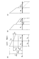
(第1実施形態)
本発明の第1実施形態による不揮発性半導体記憶装置は、例えば、マトリクス状に配置されたNANDセルユニットを有している、各NANDセルユニットは、直列に接続されたメモリセルで形成されたNANDセルを含んでいる。各メモリセルMCは、図1に示すように、p型のSi基板1に離間して形成された、n型不純物(例えば、P(リン)やAs(ヒ素))を含むn型ソース領域2aおよびドレイン領域2bを備えている。ソース領域2aとドレイン領域2bとの間のSi基板1上にトンネル絶縁膜3が形成され、このトンネル絶縁膜3上に電荷蓄積膜4が形成され、この電荷蓄積膜4上に電極間絶縁膜5が形成され、この電極間絶縁膜5上に制御ゲート電極6が形成された構成となっている。そして、制御ゲート電極6、電極間絶縁膜5、電荷蓄積膜4、およびトンネル絶縁膜3からなる積層構造のゲートは、シリコン酸化膜7によって覆われている。ここで、電荷蓄積膜4として、浮遊ゲート電極を用いてFG型の不揮発性半導体記憶装置にしても良いし、トラップ絶縁膜を用いていわゆるMONOS型の不揮発性半導体記憶装置にしても良い。
(First embodiment)
The nonvolatile semiconductor memory device according to the first embodiment of the present invention has, for example, NAND cell units arranged in a matrix. Each NAND cell unit is a NAND formed of memory cells connected in series. Contains cells. As shown in FIG. 1, each memory cell MC includes an n-
トンネル絶縁膜3は、図2に示すように、ホールを捕獲し放出するレベル(アシストレベル)を有さない低誘電率(low−k)材料の絶縁層8と、この上に形成された、ホールのアシストレベルを有する高誘電率(high−k)材料の絶縁層9との積層構造を有している。本実施形態のトンネル絶縁膜は、従来のトンネル絶縁膜とは構造が決定的に異なっている。すなわち、本発明者達によって発明され既に特許出願された特開2008−147390号公報におけるトンネル絶縁膜は、電子のアシストレベルのあるSiO2膜であり、同じ膜の両端だけに電子のアシストレベルを有する三層構造の膜であるのに対し、本実施形態における積層構造は、異なる誘電率の絶縁層の二層の積層構造であり、ホールのアシストレベルが形成されたものである。前者ではトンネル絶縁膜は必ず膜厚方向に対称であり、また低誘電体膜にだけアシストレベルを形成しなければならないのに対して、後者では対称である必要がなく、また膜全体にアシストレベルを形成することができる。また、特許第3357861号公報に記載された異なる誘電率の絶縁層の積層構造のトンネル絶縁膜はアシストレベルが無いのに対し、本実施形態におけるトンネル絶縁膜の積層構造は、ホールのアシストレベルが形成されている。
As shown in FIG. 2, the
図3は、図2に示す積層構造のトンネル絶縁膜に電界がかかっていない場合(Eox=0)のエネルギーバンドの模式図である。図3の左から、半導体基板のフェルミレベルEFを示し、次はlow−k材料からなる絶縁層(以下、low−k層とも云う)の伝導帯の下端(CBM; Conduction Band Minimum)ECと、価電子帯の上端(VBM; Valence Band Maximum)EVを示し、次はhigh−k材料からなる絶縁層(以下、high−k層とも云う)における伝導帯の下端EC、アシストレベル、および価電子帯の上端EVを示し、最後は電荷蓄積膜5のフェルミレベルEFを示している。なお、ここでいう半導体基板のフェルミレベルEFとは、半導体基板を強反転させた状態(消去の状態)での表面でのフェルミレベルのことであり、通常、半導体基板の価電子帯の上端Evより約0.1eV程度だけ低い位置にある。また、low−kおよびhigh−kの絶縁層の物理的な厚さ(物理層厚と呼ぶ)をそれぞれT1およびT2とし、low−k層およびhigh−k層のそれぞれの価電子帯の上端EVと半導体基板のフェルミレベルEFとの差、つまりホールに対するバリアハイトは、それぞれφb1およびφb2とする。ここでは、ホールのアシストレベルは、high−k層の価電子帯の上端EVからの深さφt2で定義した。なお、バリアハイトおよびアシストレベルはエネルギー軸では負の値であるが、絶対値(正の値)として表記する。アシストレベルは、半導体基板のフェルミレベルEFから見ると、φb1−φt2のレベルにあることになる。なお、半導体基板、電荷蓄積膜それぞれのEC、EVは省略した。また、図3ではEox=0のときに半導体基板と電荷蓄積膜のフェルミレベルEFが揃っているように描かれているが、必ずしも揃っている必要はない。
FIG. 3 is a schematic diagram of an energy band when no electric field is applied to the tunnel insulating film having the stacked structure illustrated in FIG. 2 (E ox = 0). From the left of FIG. 3 shows the Fermi level E F of the semiconductor substrate, next an insulating layer made of low-k material (hereinafter, also referred to as low-k layer) the lower end of the conduction band of (CBM; Conduction Band Minimum) E C When valence upper end of the electron band; indicates (VBM valence band Maximum) E V , the insulating layer next made of a high-k material (hereinafter, also referred to as high-k layer) lower E C of the conduction band in, the assist level, and shows the top edge E V of the valence band, finally indicates the Fermi level E F of the
この積層構造を有するトンネル絶縁膜を流れるトンネル電流Jは、
図2に示す積層構造のトンネル絶縁膜に低い電界Eoxがかかっている場合のエネルギーバンドの模式図を図4(a)に示す。ここで、low−k層およびhigh−k層のそれぞれの誘電率をε1およびε2とし、low−k層およびhigh−k層にそれぞれかかる電圧をV1およびV2とする。誘電率が異なる絶縁層の積層構造において、電束密度が一定と仮定した場合、それぞれの絶縁層に異なる実電界がかかることになる。そのとき、low−k層およびhigh−k層にかかる実電界をE1およびE2とすると、
εox×Eox=ε1×E1=ε2×E2 (4)
となる。ここで、εox(=3.9)はSiO2の誘電率である。実電界は、E1=V1/T1、E2=V2/T2と定義した。つまり、
ε1×V1/T1=ε2×V2/T2 (5)
を満たす。(4)式からわかるように、high−k層よりもlow−k層の方の実電界が強くなる。これは、ε1<ε2であるので、E1>E2となるからである。それ故、low−k層の物理層厚T1がhigh−k層の物理層厚T2と比較してある程度厚い場合、low−k層にかかる電圧V1がhigh−k層にかかる電圧V2よりも高くなる。これは、ε1<ε2であるので、例えば、T1>T2のとき、(ε1/T1)<(ε2/T2)となる。これと(5)式から、V1>V2となるからである。
FIG. 4A shows a schematic diagram of an energy band when a low electric field E ox is applied to the tunnel insulating film having the laminated structure shown in FIG. Here, each of the dielectric constant of the low-k layer and the high-k layer and epsilon 1 and epsilon 2, the voltage across each of the low-k layer and the high-k layer and the V 1 and V 2. In a laminated structure of insulating layers having different dielectric constants, assuming that the electric flux density is constant, different actual electric fields are applied to the respective insulating layers. At that time, if the actual electric fields applied to the low-k layer and the high-k layer are E 1 and E 2 ,
ε ox × E ox = ε 1 × E 1 = ε 2 × E 2 (4)
It becomes. Here, ε ox (= 3.9) is the dielectric constant of SiO 2 . The actual electric field was defined as E 1 = V 1 / T 1 and E 2 = V 2 / T 2 . That means
ε 1 × V 1 / T 1 = ε 2 × V 2 / T 2 (5)
Meet. As can be seen from the equation (4), the actual electric field in the low-k layer is stronger than that in the high-k layer. This is because E 1 > E 2 since ε 1 <ε 2 . Therefore, when the physical layer thickness T 1 of the low-k layer is somewhat thicker than the physical layer thickness T 2 of the high-k layer, the voltage V 1 applied to the low-k layer is changed to the voltage V applied to the high-k layer. Higher than 2 . Since this is ε 1 <ε 2 , for example, when T 1 > T 2 , (ε 1 / T 1 ) <(ε 2 / T 2 ). This is because V 1 > V 2 from this and equation (5).
アシストレベルは、high−k層に電圧V2がかかるため、エネルギーレベルから見ると、V2の幅を持つことになる。しかし、この状況では、半導体基板のフェルミレベルEFはアシストレベルよりも高いため、アシストレベルはリーク電流に影響しない。つまり、低電界では、アシストレベルのない同じ積層構造の絶縁膜と同じリーク電流になる。そのときの実効トンネル確率T*(Ex)は、
TFN(φb *,m*,E)=1 (8)
で定義される。ここで、m*はトンネル絶縁膜中をトンネルしているホールの有効質量、φb *はトンネル絶縁膜の実効的なバリアハイト、E1およびE2はそれぞれlow−k層およびhigh−k層における実電界を示す。なお、F−Nトンネルとは、図5(a)に示すように、ホールが絶縁膜の傾斜した価電子帯を通り抜ける(電子の場合は伝導帯を通り抜ける)トンネルことを意味し、D−T(Direct Tunneling)とは、図5(b)に示すように、ホールが絶縁膜の価電子帯を通り抜けず、対向する電極に直接到達するトンネルのことを意味する。なお、ここではホールのトンネリングを説明しやすいように、エネルギーを示す縦軸を通常(電子の場合)とは反対向き、すなわち図において上下反対に示した。また、これより先、断り無くエネルギー軸を逆向きに取る場合もあるが、内容から逆向きであることは容易に判断できる。
Assist level, the voltage V 2 according to the high-k layer, when viewed from the energy level will have a width of V 2. However, in this situation, the Fermi level E F of the semiconductor substrate is higher than the assist level, the assist level does not affect the leakage current. That is, at a low electric field, the same leakage current as that of the insulating film having the same laminated structure without the assist level is obtained. The effective tunnel probability T * (E x ) at that time is
Defined by Here, m * is the effective mass of the hole tunneling in the tunnel insulating film, φ b * is the effective barrier height of the tunnel insulating film, and E 1 and E 2 are in the low-k layer and the high-k layer, respectively. The actual electric field is shown. As shown in FIG. 5A, the FN tunnel means a tunnel in which holes pass through the inclined valence band of the insulating film (in the case of electrons, pass through the conduction band). As shown in FIG. 5B, (Direct Tunneling) means a tunnel in which holes do not pass through the valence band of the insulating film and directly reach the opposing electrodes. Here, in order to easily explain the tunneling of holes, the vertical axis indicating energy is shown in the opposite direction to the normal case (in the case of electrons), that is, upside down in the figure. Further, there is a case where the energy axis is taken in the opposite direction without notice, but it can be easily determined from the contents that the energy axis is in the opposite direction.
図2に示す積層構造のトンネル絶縁膜に高い電界Eoxがかかっている場合のエネルギーバンド図を図4(b)に示す。電界Eoxが高いので、それぞれの膜にかかる電圧も高くなる。すると、low−k層には高い電圧V1がかかり、high−k層にはそれよりも低い電圧V2がかかる。図4(b)からわかるように、電界Eoxがある程度高い場合には、low−k層に高い電圧がかかるため、high−k層の価電子帯の上端EVがV1だけ高くなり、それに伴い、アシストレベルもV1高くなり、半導体基板のフェルミレベルEFがアシストレベルの高さと重なる。すると、ホールがアシストレベルを介してトンネルするようになる。ホールが半導体基板からアシストレベルにトンネルする確率をp1、ホールがアシストレベルから電荷蓄積膜にトンネルする確率をp2とし、アシストレベルの占有率をf(したがって、アシストレベルの非占有率は1−f)のとき、定常状態において、電流密度の連続性から、アシストレベルを介してホールが流れる確率Pは、
P=p1×(1−f)=p2×f (9)
を満たす。このとき、f=p1/(p1+p2)となるので、
P=1/(1/p1+1/p2) (10)
となる。アシストレベルを介さない場合の確率はp1とp2の積、p1×p2であり、(10)式よりも小さな値となる。それゆえ、アシストレベルを介するとリーク電流は、アシストレベルを介さない場合よりも高くなる。
FIG. 4B shows an energy band diagram when a high electric field E ox is applied to the tunnel insulating film having the laminated structure shown in FIG. Since the electric field E ox is high, the voltage applied to each film is also high. Then, low-k layer takes a high voltage V 1, the high-k layer lower voltage V 2 is applied than that. As can be seen from FIG. 4 (b), when the electric field E ox is relatively high, since such a high voltage to the low-k layer, the higher the upper end E V of the valence band of the high-k layer only V 1, Along with this, the assist level V 1 increases, the Fermi level E F of the semiconductor substrate overlaps the height of the assist level. Then, the hole will tunnel through the assist level. The probability that a hole tunnels from the semiconductor substrate to the assist level is p 1 , the probability that the hole tunnels from the assist level to the charge storage film is p 2 , and the assist level occupation ratio is f (therefore, the assist level non-occupancy ratio is 1). -F), in a steady state, from the continuity of the current density, the probability P that holes flow through the assist level is
P = p 1 × (1−f) = p 2 × f (9)
Meet. At this time, since f = p 1 / (p 1 + p 2 ),
P = 1 / (1 / p 1 + 1 / p 2 ) (10)
It becomes. The probability of not passing through the assist level is the product of p 1 and p 2 , p 1 × p 2 , which is smaller than the expression (10). Therefore, the leakage current is higher when the assist level is used than when the assist level is not used.
Low−k層とhigh−k層の積層構造を有するトンネル絶縁膜において、high−k層にだけアシストレベルがある場合には、トンネルするホールのエネルギーレベルExとφT2の位置関係によってトンネル確率は図6(a)乃至6(c)に示すように場合分けされ、次のようにまとめられる。
φT2 *=φT2−φb2 *
と定義した。
In the tunnel insulating film having a stacked structure of the Low-k layer and the high-k layer, if there is only assist level in the high-k layer is the tunneling probability by positional relationship of energy levels E x and phi T2 hole tunneling Are classified into cases as shown in FIGS. 6A to 6C and summarized as follows.
φ T2 * = φ T2 -φ b2 *
Defined.
電子がアシストレベルを介さないでトンネルする場合(図6(a)、6(c))は、high−k層とlow−k層のそれぞれをトンネルする確率の積で表され、アシストレベルのない場合の(6)式と同じになる。アシストレベルを介してトンネルする場合(図6(b))は、
このように、低電界ではアシストレベルがリーク電流に影響しないので、high−k層を用いてトンネル絶縁膜の物理膜厚を厚くできる効果により、リーク電流が低く抑えられ、高電界ではアシストレベルを介するためホールのトンネリング確率が高くなり、したがってアシストレベル無しの場合に較べてリーク電流を大きくすることができる。アシストレベルは、high−k層中において、半導体基板から注入される電子をすべてトラップするくらいあることが望ましく、少なくとも1.0×1016cm−3以上あれば、高電界においてリーク電流を高くする効果がある。 As described above, since the assist level does not affect the leakage current in a low electric field, the leakage current can be suppressed low due to the effect of increasing the physical thickness of the tunnel insulating film using the high-k layer, and the assist level can be increased in a high electric field. Therefore, the hole tunneling probability is increased, and therefore, the leakage current can be increased as compared with the case without the assist level. It is desirable that the assist level is such that all electrons injected from the semiconductor substrate are trapped in the high-k layer. If the assist level is at least 1.0 × 10 16 cm −3 , the leakage current is increased in a high electric field. effective.
本実施形態のような積層構造のトンネル絶縁膜として、例えば、low−k層としてSiO2層、アシストレベルのあるhigh−k層としてRuを添加したHfO2層の積層絶縁膜がある。SiO2の誘電率ε1は3.9、Ruを添加したHfO2の誘電率ε2は18、シリコン基板のフェルミレベルEFに対するlow−k層のホールのバリアハイトφb1は3.8eV、high−k層のバリアハイトφb2は3.0eVである(例えば、J. Widiez et al., Jpn. J. Appl. Phys., 47, 2410 (2008)., H. Bachhofer et al., J. Appl. Phys., 89, 2791 (2001).参照)。この構成における、Eox=0の場合のバンド図を図7に示す。ここでは、トンネル絶縁膜として、EOT(Teq,all)が2.2nmの極薄膜の例として揚げる。low−k層のEOT(Teq1)は1.21nm、EOTはSiO2膜に換算した膜厚の意味なので、SiO2層の物理膜厚T1も同じく1.21nmである。High−k層のEOT(Teq2)は0.97nm、物理膜厚T2は4.50nm(=0.97×18/3.9)である。アシストレベルは、HfO2層に、例えば、Ruを添加することによって形成される。本発明者達の計算結果によれば、ホールのアシストレベルφt2は1.1eVである。なお、図7の横軸は物理膜厚Tphysを表し、縦軸はエネルギーを表す。 As a tunnel insulating film having a laminated structure as in this embodiment, for example, there is a laminated insulating film of an SiO 2 layer as a low-k layer and an HfO 2 layer to which Ru is added as a high-k layer having an assist level. Dielectric constant epsilon 1 of SiO 2 is 3.9, HfO 2 dielectric constant epsilon 2 is 18 with the addition of Ru, the hole of the low-k layer of the silicon substrate with respect to the Fermi level E F barrier height phi b1 is 3.8 eV, high The barrier height φ b2 of the −k layer is 3.0 eV (for example, J. Widiez et al., Jpn. J. Appl. Phys., 47 , 2410 (2008)., H. Bachhofer et al., J. Appl Phys., 89 , 2791 (2001)). FIG. 7 shows a band diagram when E ox = 0 in this configuration. Here, the tunnel insulating film is an example of an ultrathin film having an EOT (T eq, all ) of 2.2 nm. Since the EOT (T eq1 ) of the low-k layer is 1.21 nm and EOT means the film thickness converted to the SiO 2 film, the physical film thickness T 1 of the SiO 2 layer is also 1.21 nm. The EOT (T eq2 ) of the high-k layer is 0.97 nm, and the physical film thickness T 2 is 4.50 nm (= 0.97 × 18 / 3.9). The assist level is formed by adding, for example, Ru to the HfO 2 layer. According to the calculation results of the present inventors, the hole assist level φ t2 is 1.1 eV. In FIG. 7, the horizontal axis represents the physical film thickness T phys and the vertical axis represents energy.
EOTを2.2nmにした上述の2層構造のトンネル絶縁膜にかかる電界Eoxと、このトンネル絶縁膜を流れるリーク電流との関係は図8A、8Bに示すようになる。図8A、8Bには、比較のために、アシストレベルのない積層絶縁膜(Ruが添加されていない積層絶縁膜)の場合と、さらに、SiO2層の層厚が5nm、2.2nmの単層構造の絶縁膜の場合も示した。なお、EOTが2.2nmの単層構造のHfO2層の場合、リーク電流は、非常に低くなるため、これらの図8A、8Bに示す範囲の中には収まらず、図示していない。図8Aはホールによるリーク電流の場合を示し、図8Bは電子によるリーク電流の場合を示す。 8A and 8B show the relationship between the electric field E ox applied to the tunnel insulating film having the above-mentioned two-layer structure with an EOT of 2.2 nm and the leakage current flowing through the tunnel insulating film. 8A and 8B, for comparison, a case of a laminated insulating film without an assist level (a laminated insulating film to which Ru is not added) and a single layer having a SiO 2 layer thickness of 5 nm and 2.2 nm are shown. The case of an insulating film having a layer structure is also shown. In the case of an HfO 2 layer having a single-layer structure with an EOT of 2.2 nm, the leakage current is very low, so it does not fall within the range shown in FIGS. 8A and 8B and is not shown. FIG. 8A shows the case of leakage current due to holes, and FIG. 8B shows the case of leakage current due to electrons.
図8A、8Bの各3MV/cmにおける十字印は、電荷保持で求められるホール、電子それぞれのリーク電流のスペックを表しており、これ以下にリーク電流を低くしなければならない。一方で、図8Aにおいて、13MV/cmにおける十字印は消去に求められるスペックであり、図8Bにおいて、13MV/cmにおける十字印は書込に求められるスペックである。どちらも、十字印に示す値以上のリーク電流であることが求められる。消去の場合には、トンネル絶縁膜に高い正の電界Eoxをかけることになる。一般的に、消去特性として求められるスペックは、層厚が5nmのSiO2層における消去特性より同等かあるいはそれ以上であり、例えば、電界13MV/cmでホールのリーク電流1×10−5A/cm2以上である。 The cross marks at 3 MV / cm in FIGS. 8A and 8B represent the specifications of the leak currents of holes and electrons required for charge retention, and the leak current must be lower than this. On the other hand, in FIG. 8A, the cross mark at 13 MV / cm is a specification required for erasing, and in FIG. 8B, the cross mark at 13 MV / cm is a specification required for writing. Both are required to have a leakage current equal to or greater than the value indicated by the cross. In the case of erasing, a high positive electric field E ox is applied to the tunnel insulating film. In general, specifications required as erasing characteristics, the layer thickness is at equal to or higher than the erase characteristics in the SiO 2 layer of 5 nm, for example, the holes in the field 13 MV / cm leakage current 1 × 10 -5 A / cm 2 or more.
図8Aからわかるように、SiO2層の層厚が5nmの場合にはこのスペックを満たすことができ(図8Aの十字印)、SiO2層の層厚が2.2nmの場合には更に多くのリーク電流を流すことができる。しかし、膜厚が2.2nmでは、3MV/cmにおける低電界のリーク電流が十字印に示す値以上となり、電荷保持特性と消去特性のスペックを同時には満たせない。また、積層構造の絶縁膜の場合でも、アシストレベルが無い膜(例えば、Ruが添加されない膜)では、リーク電流は13MV/cmで2×10−13A/cm2となり、求められているスペック2×10−5A/cm2に較べて、8桁も及ばない。 As can be seen from FIG. 8A, this specification can be satisfied when the layer thickness of the SiO 2 layer is 5 nm (the cross mark in FIG. 8A), and more when the layer thickness of the SiO 2 layer is 2.2 nm. Leakage current. However, when the film thickness is 2.2 nm, the leakage current of a low electric field at 3 MV / cm is not less than the value indicated by the cross mark, and the specifications for the charge retention characteristic and the erasing characteristic cannot be satisfied at the same time. Further, even in the case of an insulating film having a laminated structure, in a film without an assist level (for example, a film to which Ru is not added), the leakage current is 2 × 10 −13 A / cm 2 at 13 MV / cm, and required specifications. Compared to 2 × 10 −5 A / cm 2 , it does not reach 8 digits.
前述したように、ホールがlow−k層とhigh−k層の順に流れる場合には、high−k層の価電子帯の上端EVが高くなり、ホールのバリアハイトが低くなるので、リーク電流は増える方向であり、ある程度の膜厚では効果のある構造となる。しかしながら、トンネル絶縁膜のEOT(Teq,all)の薄膜化を進めると、同じEoxでもその定義(Eox=Vins/Teq,all)から、トンネル絶縁膜にかかるVinsも小さくしなければならない。このように、電圧は小さくなるものの、バリアハイトは膜の性質で決まっている値のため、小さくはならない。それゆえ、アシストレベルの無い積層構造のトンネル絶縁膜では、13MV/cmの電界では充分にリーク電流を高くすることはできない。 As described above, if the hole flows in the order of the low-k layer and the high-k layer has an upper end E V of the valence band of the high-k layer is increased, since the barrier height of the hole is lowered, the leakage current This is an increasing direction, and an effective structure is obtained with a certain film thickness. However, if EOT (T eq, all ) of the tunnel insulating film is made thinner, V ins applied to the tunnel insulating film is also reduced from the definition (E ox = V ins / T eq, all ) even with the same E ox. There must be. Thus, although the voltage is small, the barrier height is not a small value because it is a value determined by the properties of the film. Therefore, in a tunnel insulating film having a laminated structure without an assist level, a leak current cannot be sufficiently increased with an electric field of 13 MV / cm.
その一方で、アシストレベルのある積層構造のトンネル絶縁膜では、13MV/cmで消去に求められるスペックを満たすことができる。図8Aの13MV/cmにおけるリーク電流を見るとわかるように、消去に求められるスペックを表す十字印の値を大幅に上回るリーク電流が流れている。これは、高速に消去できることや、低電界で消去できることを示している。 On the other hand, a tunnel insulating film having a laminated structure with an assist level can satisfy the specifications required for erasing at 13 MV / cm. As can be seen from the leakage current at 13 MV / cm in FIG. 8A, a leakage current that greatly exceeds the value of the cross mark indicating the specifications required for erasing flows. This indicates that it can be erased at high speed and can be erased with a low electric field.
この積層構造のトンネル絶縁膜は、電子によるリーク電流に求められるスペック、つまり、電荷保持や書込特性に求められるスペックを同時に満たすように形成することができる。図8Bにおいて、電界が正の3MV/cmのときに、電荷を保持するために、電子によるリーク電流は1×10−16A/cm2以下でなければならないが、それを充分に満たしている。また、電界が−13MV/cmの場合に、書込特性を満たすために、電子によるリーク電流は、0.1A/cm2以上であることが求められるが、それも満足している。 This tunnel insulating film having a laminated structure can be formed so as to simultaneously satisfy specifications required for a leakage current due to electrons, that is, specifications required for charge retention and writing characteristics. In FIG. 8B, when the electric field is positive 3 MV / cm, the leakage current due to electrons must be 1 × 10 −16 A / cm 2 or less in order to hold the electric charge, which is sufficiently satisfied. . Further, when the electric field is −13 MV / cm, in order to satisfy the writing characteristics, the leakage current due to electrons is required to be 0.1 A / cm 2 or more, which is also satisfied.
こうして、本実施形態のように、ホールのアシストレベルのあるhigh−k絶縁層と、low−k絶縁層との積層構造からなるトンネル絶縁膜は、Eoxが13MV/cmの高電界においてホールのリーク電流が1×10−5A/cm2以上になり、消去効率を向上させられると同時に、3MV/cmで1×10−16cm−2以下にできるため電荷保持のスペックを満たし、−13MV/cmで0.1A/cm2以上になるので書込み効率のスペックも充分に満足させながら、SiO2膜では無理であった5nm以下の薄膜化も可能であり、EOTで2.2nmにすることができる。 Thus, as in this embodiment, a tunnel insulating film having a stacked structure of a high-k insulating layer having a hole assist level and a low-k insulating layer has a high electric field with an E ox of 13 MV / cm. The leakage current becomes 1 × 10 −5 A / cm 2 or more, and the erase efficiency can be improved. At the same time, it can be reduced to 1 × 10 −16 cm −2 or less at 3 MV / cm, so that the charge retention specification is satisfied, and −13 MV Since it becomes 0.1 A / cm 2 or more at / cm, it is possible to reduce the thickness to 5 nm or less, which is impossible with the SiO 2 film, while sufficiently satisfying the specifications of the writing efficiency. Can do.
以上説明したように、本実施形態によれば、EOTを薄くしても低電界におけるリーク電流を抑制することが可能となるとともに高電界におけるホールのリーク電流を高くすることが可能となるトンネル絶縁膜を有する不揮発性半導体記憶装置を提供することができる。 As described above, according to this embodiment, even if the EOT is thinned, it is possible to suppress the leakage current in the low electric field and increase the hole leakage current in the high electric field. A nonvolatile semiconductor memory device having a film can be provided.
(積層構造のトンネル絶縁膜の膜厚範囲)
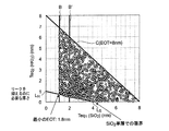
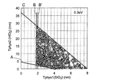
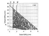
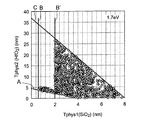
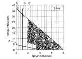
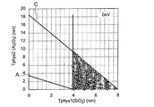
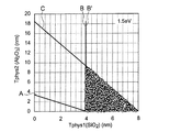
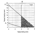
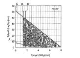
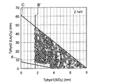
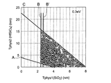
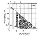
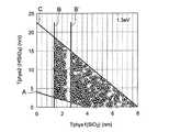
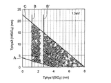
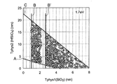
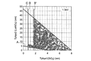
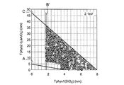
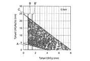
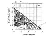
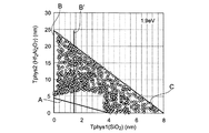
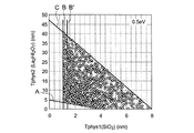
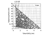
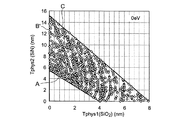
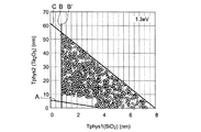
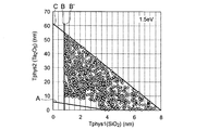
次に、第1実施形態の不揮発性半導体記憶装置において、積層構造のトンネル絶縁膜は、どの膜厚範囲であれば、トンネル絶縁膜として要求されるスペックを満たすかを調べた。SiO2層のEOTすなわちTeq1(SiO2)を横軸に、HfO2層のEOTすなわちTeq2(HfO2)を縦軸にとって、トンネル絶縁膜として求められるスペックを満たす範囲を図9に示す。つまり、当然ながら、点で示したところだけでなく、それ以外の、点と点の間の領域も含まれる。なお、SiO2層とHfO2層の両方を合わせたEOT(Teq,all)の上限を8nmとした。この上限は、図9において、直線C(Teq1+Teq2=8)で表される。それ故、図9に示す、Teq1+Teq2>8となる領域(直線Cより上の領域)は、スペックを満たす範囲に含まれていない。図9において、直線Aは低電界でリーク電流を抑えるのに最低限必要な膜厚の割合を示している。直線Aと横軸が交わる点LSは、SiO2層だけの場合であり、電荷保持するのに、ホールによる電流の場合、SiO2層が約4nmが必要であることを示している。ちなみに、電子による電流の場合は5nmであった。そして、直線Aと縦軸が交わる点LHは、HfO2層だけの場合であり、直線AはSiO2層とHfO2層の積層構造が電荷保持するのに必要な最低限必要な膜厚を表している。
(Thickness range of laminated tunnel insulating film)
Next, in the nonvolatile semiconductor memory device of the first embodiment, it was examined in which film thickness range the tunnel insulating film having a laminated structure satisfies the specifications required for the tunnel insulating film. FIG. 9 shows a range that satisfies the specifications required for the tunnel insulating film, with the EOT of the SiO 2 layer, ie, T eq1 (SiO 2 ) on the horizontal axis, and the EOT of the HfO 2 layer, ie, T eq2 (HfO 2 ), on the vertical axis. That is, as a matter of course, not only the points indicated by the points but also other regions between the points are included. In addition, the upper limit of EOT (T eq, all ) combining both the SiO 2 layer and the HfO 2 layer was 8 nm. This upper limit is represented by a straight line C (T eq1 + T eq2 = 8) in FIG. Therefore, the region (region above the straight line C) where T eq1 + T eq2 > 8 shown in FIG. 9 is not included in the range satisfying the specifications. In FIG. 9, a straight line A indicates the ratio of the minimum film thickness necessary for suppressing the leakage current with a low electric field. Straight line A and the horizontal axis intersects a point L S is the case of only the SiO 2 layer, to be charge retention, when the current due to holes, indicating that the SiO 2 layer is required about 4 nm. Incidentally, in the case of the current due to electrons, it was 5 nm. The point L H where the straight line A and the vertical axis intersect is the case of only the HfO 2 layer, and the straight line A is the minimum necessary film thickness necessary for charge retention in the laminated structure of the SiO 2 layer and the HfO 2 layer. Represents.
図9からわかるように、HfO2層だけでは、スペックを満たす領域に入っていない。つまり、HfO2層だけでは、トンネル絶縁膜として使えない、ということを意味している。これは、高電界でリーク電流を高くすることができないからである。高電界でリーク電流のスペックを満たすのに最低限必要なSiO2層の厚さは、直線Bおよび直線B’で表される。直線B’は、HfO2層にアシストレベルが無い場合のトンネル絶縁膜において最低限必要なSiO2層の層厚を表している。その層厚は2.0nmである。SiO2層とHfO2層との積層構造を有するトンネル絶縁膜において、アシストレベルがない場合でも、このように、SiO2層の層厚が2.0nm以上あれば層厚が4.0nmの単層となるSiO2層よりも薄膜のトンネル絶縁膜が形成でき、この構造の場合にはトンネル絶縁膜全体のEOTとして2.6nmまで薄膜化できる(直線Aと直線B’の交点)。 As can be seen from FIG. 9, the HfO 2 layer alone does not enter the region that satisfies the specifications. That is, it means that the HfO 2 layer alone cannot be used as a tunnel insulating film. This is because the leakage current cannot be increased with a high electric field. The minimum thickness of the SiO 2 layer required to satisfy the leakage current specifications with a high electric field is represented by a straight line B and a straight line B ′. A straight line B ′ represents the minimum layer thickness of the SiO 2 layer required for the tunnel insulating film when the HfO 2 layer has no assist level. The layer thickness is 2.0 nm. In the tunnel insulating film having a stacked structure of a SiO 2 layer and the HfO 2 layer, even if there is no assist level, thus, the layer thickness if the layer thickness of SiO 2 layers or more 2.0nm is 4.0nm single A tunnel insulating film having a thickness smaller than that of the SiO 2 layer can be formed. In this structure, the tunnel insulating film can be made as thin as 2.6 nm as an EOT of the entire tunnel insulating film (intersection of straight line A and straight line B ′).
そして、HfO2層にRuを添加してアシストレベルを形成すれば、さらに、SiO2層を半分以下の1.1nmまで薄膜化でき、HfO2層と合わせて、EOTが1.8nmの極薄のトンネル絶縁膜が形成できる。これは、アシストレベルが無い場合のSiO2層の膜厚2.0nmよりも薄い膜厚である。アシストレベルが無いときに、SiO2層を薄くできない理由は、次のように説明できる。電界が高いときにリーク電流は高くならなければならない。そのためには、HfO2層の価電子帯の上端Evが充分に高くなり、ホールのバリアハイトが低くなって、ホールがトンネルし易くする必要がある。しかし、電界Eox(=V1/Teq1)が同じままSiO2層の膜厚Teq1を薄くすると、SiO2層にかかる電圧V1は小さくなるので、充分にHfO2層の価電子帯の上端EVが上がらなくなり、したがって、リーク電流が高くできない。これに対して、HfO2層にアシストレベルがあれば、充分にHfO2層の価電子帯の上端EVが上がらなくても、アシストレベルを介することによって、ホールのトンネル確率が高くなる。それゆえ、アシストレベルがあるHfO2層を含む積層構造の場合には、アシストレベルがない場合よりもさらにSiO2層の薄膜化が可能になり、トンネル絶縁膜全体のEOTが1.8nmまで薄膜化できる(直線Aと直線Bの交点)。 If Ru is added to the HfO 2 layer to form an assist level, the SiO 2 layer can be further thinned to 1.1 nm, which is half or less, and combined with the HfO 2 layer, the EOT is 1.8 nm. The tunnel insulating film can be formed. This is a film thickness thinner than 2.0 nm of the SiO 2 layer when there is no assist level. The reason why the SiO 2 layer cannot be made thin when there is no assist level can be explained as follows. The leakage current must be high when the electric field is high. For this purpose, the upper end Ev of the valence band of the HfO 2 layer needs to be sufficiently high, the hole barrier height is lowered, and the holes need to be easily tunneled. However, when an electric field E ox (= V 1 / T eq1) is made thinner T eq1 remain the same SiO 2 layer, the voltages V 1 applied to the SiO 2 layer is reduced, the valence band of sufficiently HfO 2 layer the upper end E V is no longer rise, therefore, can not be high leakage current. In contrast, if the assist level HfO 2 layer, sufficiently without rise upper end E V of the valence band of the HfO 2 layer, by passing through the assist level, the tunneling probability of the holes is increased. Therefore, in the case of the laminated structure including the HfO 2 layer having the assist level, the SiO 2 layer can be made thinner than the case without the assist level, and the EOT of the entire tunnel insulating film is reduced to 1.8 nm. (Intersection of straight line A and straight line B).
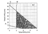
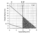
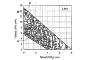
図10は、図9に示すデータを物理層厚に換算したものであり、横軸Tphys1(SiO2)は図9の横軸と同じ値となるが、縦軸Tphys2(HfO2)だけがHfO2層とSiO2層の誘電率の比の分だけスケーリングされている。それゆえ、積層構造において必要なSiO2層の物理層厚は図9に示す場合と同じであり、アシストレベルがない場合には1.8nm、アシストレベルがある場合には0.9nmである。そして、HfO2層は、物理層厚として3nmから28nmの範囲を取れる。なお、ZrO2層は、HfO2層と同じ特性を有しているので、HfO2層の代わりにZrO2層を用いることができる。 FIG. 10 is obtained by converting the data shown in FIG. 9 into a physical layer thickness. The horizontal axis T phys1 (SiO 2 ) has the same value as the horizontal axis in FIG. 9, but only the vertical axis T phys2 (HfO 2 ). Is scaled by the ratio of the dielectric constant of the HfO 2 layer and the SiO 2 layer. Therefore, the physical layer thickness of the SiO 2 layer required in the laminated structure is the same as that shown in FIG. 9, 1.8 nm when there is no assist level, and 0.9 nm when there is an assist level. The HfO 2 layer can have a physical layer thickness ranging from 3 nm to 28 nm. Incidentally, ZrO 2 layer, since they have the same characteristics as HfO 2 layer, can be used ZrO 2 layer in place of the HfO 2 layer.
(第2実施形態)
次に、本発明の第2実施形態による不揮発性半導体記憶装置を説明する。第1実施形態の不揮発性半導体記憶装置においては、トンネル絶縁膜は、high−k層だけにアシストレベルが形成されていたが、本実施形態の不揮発性半導体記憶装置においては、high−k層だけでなく、low−k層にもアシストレベルが形成されたトンネル絶縁膜を有している。第2実施形態の不揮発性半導体記憶装置は、トンネル絶縁膜以外、第1実施形態と同じ構成となっている。
(Second Embodiment)
Next, a nonvolatile semiconductor memory device according to a second embodiment of the present invention is described. In the nonvolatile semiconductor memory device of the first embodiment, the tunnel insulating film has the assist level formed only in the high-k layer. However, in the nonvolatile semiconductor memory device of the present embodiment, only the high-k layer is formed. In addition, the low-k layer has a tunnel insulating film in which an assist level is formed. The nonvolatile semiconductor memory device of the second embodiment has the same configuration as that of the first embodiment except for the tunnel insulating film.
本実施形態のトンネル絶縁膜の、Eox=0におけるエネルギーバンド図は、図3に示すlow−k層にアシストレベルφt1を付け加えた図12に示すようになる。そして、同様に、本実施形態のトンネル絶縁膜に低い電界と高い電界をかけた場合は、図4(a)、4(b)に示すlow−k層にアシストレベルφt1を付け加えた図12(a)、12(b)に示すようにそれぞれなる。これらの場合は、図12(a)、12(b)に示すように、low−k層のアシストレベルがリーク電流に寄与しないので、low−k層にアシストレベルがあっても無くても、リーク電流に変化がない、つまり、書込み効率は変わらない。low−k層のアシストレベルがリーク電流に寄与すれば、書込み効率は上がることになるが、そのときには電荷保持特性が劣化してしまう場合もあるし、条件によっては電荷保持特性が維持される場合もある。 The energy band diagram of the tunnel insulating film of the present embodiment at E ox = 0 is as shown in FIG. 12 in which the assist level φ t1 is added to the low-k layer shown in FIG. Similarly, when a low electric field and a high electric field are applied to the tunnel insulating film of the present embodiment, FIG. 12 is obtained by adding an assist level φ t1 to the low-k layers shown in FIGS. (A) and 12 (b), respectively. In these cases, as shown in FIGS. 12A and 12B, the assist level of the low-k layer does not contribute to the leakage current. There is no change in the leakage current, that is, the writing efficiency does not change. If the assist level of the low-k layer contributes to the leakage current, the writing efficiency is increased. At that time, the charge retention characteristic may be deteriorated, or the charge retention characteristic is maintained depending on conditions. There is also.
以上説明したように、本実施形態のように、トンネル絶縁膜のlow−k層とhigh−k層の両方にアシストレベルが形成されていても、要求されるスペックを満たす極薄EOTを有するトンネル絶縁膜が得ることが可能となる。これにより、EOTを薄くしても低電界におけるリーク電流を抑制することが可能となるとともに高電界におけるリーク電流を高くすることが可能なトンネル絶縁膜を有する不揮発性半導体記憶装置を提供することができる。 As described above, as in the present embodiment, a tunnel having an ultra-thin EOT that satisfies the required specifications even when the assist level is formed in both the low-k layer and the high-k layer of the tunnel insulating film. An insulating film can be obtained. Accordingly, it is possible to provide a nonvolatile semiconductor memory device having a tunnel insulating film that can suppress a leakage current in a low electric field and increase a leakage current in a high electric field even if the EOT is thinned. it can.
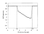
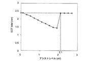
(アシストレベルについて)
ここまでは、アシストレベルとして、1.1eVの場合だけを示したが、他の値でも構わない。しかしながら、アシストレベルの値は何でも良いわけではなく、本発明の上記実施形態における効果を得るためには、以下に説明する範囲にあることが好ましい。
(Assist level)
Up to this point, only the case where the assist level is 1.1 eV is shown, but other values may be used. However, the value of the assist level is not limited to anything, and in order to obtain the effect in the above embodiment of the present invention, it is preferably in the range described below.
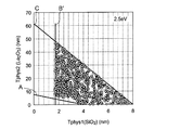
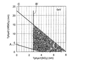
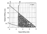
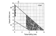
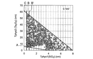
図13A乃至図13Pは、様々なアシストレベルを有するHfO2層と、SiO2層との積層構造からなるトンネル絶縁膜において、本発明の一実施形態で定義したスペックを満たすHfO2層とSiO2層の物理膜厚Tphysの範囲を示した図である。アシストレベルの大きさによって、特にSiO2層の物理膜厚の範囲が変化することがわかる。図13A乃至図13Pはそれぞれ、HfO2層のアシストレベルが0eV、0.1eV、0.3eV、0.5eV、0.7eV、0.9eV、1.1eV、1.3eV、1.5eV、1.7eV、1.9eV、2.1eV、2.3eV、2.5eV、2.7eV、2.9eVの場合の図である。そして、これらのアシストレベルと、トンネル絶縁膜のEOTとの関係を図14に示す。ここで、アシストレベルが0eVは、アシストレベルが無い場合を示しており、前述したように、そのとき最小のEOTは2.5nmとなる。図14からわかるように、アシストレベルが価電子帯の上端から深くなるほど、アシストレベルがない場合に較べて、トンネル絶縁膜のEOTが薄膜化できる。アシストレベルが2.1eVのときEOTが最小となり、そのEOTは約1.19nmに到達する。そして、それよりも深くなると、急激にEOTの膜厚は厚くなり、例えば、2.3eVのときには、EOTは3.6nmとなり、アシストレベルのない場合よりも厚くなる。これは、HfO2層中のアシストレベルが深いと、層厚の薄いHfO2層では、低い電界Eoxでもアシストレベルを介したリーク電流が支配的になり、したがって低電界でのスペックを満たさないからである。つまり、アシストレベルとしては、0eVより大きく、2.2eV未満であることが好ましい。そして、最も適する欠陥形態はHfO2中のHfをRuが置換したものが好ましいことがわかった。なお、アシストレベルがある場合には、そのlow−k層の層厚(直線Bと横軸との交点の値)を、アシストレベルが無い場合に必要なlow−k層の層厚(直線B’と横軸との交点の値)よりも薄くすることができる(図13F乃至図13I)。上述の説明ではlow−k層がSiO2層であって、high−k層がHfO2層であったが、low−k層が酸化シリコン層でhigh−k層がハフニア(HfO)層である場合でもアシストレベルが上述の範囲であれば同様の範囲で同様の効果を得ることができる。 13A to 13P illustrate a tunnel insulating film having a laminated structure of an HfO 2 layer having various assist levels and an SiO 2 layer, and the HfO 2 layer and the SiO 2 satisfying the specifications defined in the embodiment of the present invention. It is the figure which showed the range of the physical film thickness Tphys of a layer. It can be seen that the physical film thickness range of the SiO 2 layer varies depending on the size of the assist level. 13A to 13P, the assist levels of the HfO 2 layer are 0 eV, 0.1 eV, 0.3 eV, 0.5 eV, 0.7 eV, 0.9 eV, 1.1 eV, 1.3 eV, 1.5 eV, 1 7 eV, 1.9 eV, 2.1 eV, 2.3 eV, 2.5 eV, 2.7 eV, and 2.9 eV. FIG. 14 shows the relationship between these assist levels and the EOT of the tunnel insulating film. Here, an assist level of 0 eV indicates a case where there is no assist level. As described above, the minimum EOT is 2.5 nm as described above. As can be seen from FIG. 14, the deeper the assist level from the upper end of the valence band, the thinner the EOT of the tunnel insulating film, compared to the case where there is no assist level. When the assist level is 2.1 eV, the EOT is minimized, and the EOT reaches about 1.19 nm. When it becomes deeper than that, the EOT film thickness suddenly increases. For example, at 2.3 eV, EOT becomes 3.6 nm, which is thicker than when there is no assist level. This is because when the assist level in the HfO 2 layer is deep, in the thin HfO 2 layer, the leakage current via the assist level is dominant even at a low electric field E ox , and thus the specification in the low electric field is not satisfied. Because. That is, the assist level is preferably greater than 0 eV and less than 2.2 eV. It was found that the most suitable defect form is preferably one in which Hf in HfO 2 is replaced by Ru. When there is an assist level, the layer thickness of the low-k layer (the value of the intersection of the straight line B and the horizontal axis) is set to the layer thickness of the low-k layer (straight line B) when there is no assist level. (The value of the intersection point of 'and the horizontal axis) (Figs. 13F to 13I). In the above description, the low-k layer is an SiO 2 layer and the high-k layer is an HfO 2 layer, but the low-k layer is a silicon oxide layer and the high-k layer is a hafnia (HfO) layer. Even in this case, if the assist level is in the above range, the same effect can be obtained in the same range.
また、図14には、さらにHfO2層と、窒化シリコン(SiN)層との積層構造からなるトンネル絶縁膜の場合も示している。図14からわかるように、SiO2層をSiN層で置き換えた場合は、アシストレベルとしては、0.7eVより大きく、2.2eV未満であることが好ましい。したがって、high−k層と積層するlow−k層として、SiO2層またはSiN層を用いる場合では、好適なアシストレベルの範囲に差はあるものの、どちらを用いても構わない、と言える。さらに、low−k層としては、SiO2層とSiN層の間の性質を持つSiON層でもよいし、SiO2層/SiN層/SiO2層のように3層以上の積層構造を有していてもよい。Si、O、Nが主たる元素であれば、それ以外の元素が混ざっていても、本発明の一実施形態におけるlow−k層として機能する。 FIG. 14 also shows the case of a tunnel insulating film having a laminated structure of an HfO 2 layer and a silicon nitride (SiN) layer. As can be seen from FIG. 14, when the SiO 2 layer is replaced with a SiN layer, the assist level is preferably greater than 0.7 eV and less than 2.2 eV. Therefore, when a SiO 2 layer or a SiN layer is used as the low-k layer to be stacked with the high-k layer, it can be said that either one may be used although there is a difference in the range of a suitable assist level. Further, the low-k layer may be a SiON layer having properties between the SiO 2 layer and the SiN layer, or has a laminated structure of three or more layers such as SiO 2 layer / SiN layer / SiO 2 layer. May be. If Si, O, and N are main elements, even if other elements are mixed, it functions as a low-k layer in one embodiment of the present invention.
アシストレベルを形成する方法として、Ruを添加する例を示したが、Ru以外の元素、例えば、Cr、Mn、V、Tc、Osなどの元素によっても形成することができ、それゆえ、第1実施形態における1.1eVとは異なるアシストレベルを形成することが可能である。トンネル絶縁膜のlow−k層がSiO2層であって、high−k層がHfO2層である場合に、HfO2層に添加される元素によって形成されるアシストレベルの計算結果を図49に示す。この図49からわかるように、ホールのアシストレベルを形成するには、3d元素としてMn(0.9eV)、Cr(1.8eV)、V(2.8eV)が好ましく、4d元素としてRu(1.6eV)が好ましく、5d元素としてOs(2.15eV)が好ましい。なお、元素記号の次の括弧の数字は、HfO2の価電子帯の上端からホールのアシストレベルまでのエネルギー差を示す。また、図49からわかるように、V、Ru、Osは、HfO2層に添加されると、ホールの好適なアシストレベルだけでなく、電子の好適なアシストレベルをも形成するので、添加元素としては、更に好ましい。なお、ここで、ホールの好適なアシストレベルとは、ホールのアシストレベルが、high−k材料の価電子帯の上端からlow−k材料の価電子帯の上端までの範囲にあることを意味する。電子の好適なアシストレベルとは、電子のアシストレベルが、low−k材料の伝導帯の下端からhigh−k材料の伝導帯の下端までの範囲にあることを意味する。 Although an example in which Ru is added has been shown as a method for forming the assist level, it can also be formed by an element other than Ru, for example, an element such as Cr, Mn, V, Tc, and Os. It is possible to form an assist level different from 1.1 eV in the embodiment. When the low-k layer of the tunnel insulating film is the SiO 2 layer and the high-k layer is the HfO 2 layer, the calculation result of the assist level formed by the element added to the HfO 2 layer is shown in FIG. Show. As can be seen from FIG. 49, in order to form the hole assist level, Mn (0.9 eV), Cr (1.8 eV), and V (2.8 eV) are preferable as the 3d element, and Ru (1 .6 eV) is preferable, and Os (2.15 eV) is preferable as the 5d element. The number in parentheses next to the element symbol indicates the energy difference from the upper end of the valence band of HfO 2 to the assist level of the hole. As can be seen from FIG. 49, when V, Ru, and Os are added to the HfO 2 layer, they form not only a suitable assist level for holes but also a suitable assist level for electrons. Is more preferable. Here, the preferable assist level of the hole means that the assist level of the hole is in a range from the upper end of the valence band of the high-k material to the upper end of the valence band of the low-k material. . A suitable assist level for electrons means that the assist level for electrons is in the range from the lower end of the conduction band of the low-k material to the lower end of the conduction band of the high-k material.
また、これらの添加元素は、以下に説明する各種のhigh−k層に用いても同様に、ホールの好適なアシストレベルを形成することができる。なお、本発明者達の計算によれば、high−k層としてAl2O3を用いる場合は、ホールの好適なアシストレベルを形成する添加元素として上記元素の他に、C(炭素)を用いことができる。 Further, even when these additive elements are used in various high-k layers described below, it is possible to form a suitable assist level for holes. According to the calculations by the present inventors, when Al 2 O 3 is used as the high-k layer, C (carbon) is used in addition to the above elements as an additive element for forming a suitable assist level for holes. be able to.
(high−k層について)
以上の説明では、high−k層として、HfO2の例を示したが、他のhigh−k層でも同じ効果がある。他のhigh−k層として、例えば、図15に示す表に揚げたようなものがある(例えば、J. Robertson, J. Vac. Sci. Technol. B, 18, 1785 (2000)、
G. Yu et al., Appl. Phys. Lett, 81, 376 (2002)、G. D. Wilk et al., Symp. VLSI Tech. Dig. 88 (2002)、G. Seguini et al., Appl. Phys. Lett. 88, 202903 (2006)、またはA. Dimoulas et al., Appl. Phys. Lett. 85, 3205 (2004)参照)。これらの誘電率とバンドオフセットΔEVとの関係をプロットしたものを図16に示す。ここで、バンドオフセットΔEVとは、Si基板の価電子帯の上端EVとhigh−k層の価電子帯の上端EVとの差であり、トンネル絶縁膜においてホールのバリアハイトに対応する。
(About high-k layer)
In the above description, an example of HfO 2 is shown as the high-k layer, but the same effect can be obtained in other high-k layers. Other high-k layers include, for example, those fried in the table shown in FIG. 15 (for example, J. Robertson, J. Vac. Sci. Technol. B, 18, 1785 (2000),
G. Yu et al., Appl. Phys. Lett, 81, 376 (2002), GD Wilk et al., Symp. VLSI Tech. Dig. 88 (2002), G. Seguini et al., Appl. Phys. Lett 88, 202903 (2006), or A. Dimoulas et al., Appl. Phys. Lett. 85, 3205 (2004)). A plot of the relationship between these dielectric constant and band offset Delta] E V shown in FIG. 16. Here, the band offset Delta] E V, the difference between the upper end E V of the valence band of the upper E V and the high-k layer of the valence band of the Si substrate, corresponding to the barrier height of the hole in the tunnel insulating film.
Al 2 O 3 層
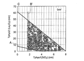
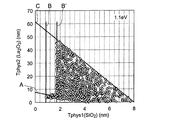
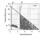
また、high−k層としてAl2O3層、low−k層としてSiO2層を選択して積層した場合の、様々なアシストレベルにおいて、本発明の一実施形態で定義したトンネル絶縁膜に求められるスペックを満たす物理膜厚の範囲を図17A乃至図17Zに示す。図17A乃至図17Zはそれぞれ、Al2O3層のアシストレベルが、0eV(無い場合)、0.1eV、0.3eV、0.5eV、0.7eV、0.9eV、1.1eV、1.3eV、1.5eV、1.7eV、1.9eV、2.1eV、2.3eV、2.5eV、2.7eV、2.9eV、3.1eV、3.3eV、3.5eV、3.7eV、3.9eV、4.1eV、4.3eV、4.5eV、4.7eV、4.9eVの場合の図である。そして、これらのアシストレベルと、トンネル絶縁膜のEOTとの関係を図18に示す。図18からわかるように、high−k層としてAl2O3層を選択した場合の、アシストレベルは1.5eV以上であり、4.1eV以下であることが好ましい。なお、アシストレベルがある場合には、そのlow−k層の層厚(直線Bと横軸との交点の値)を、アシストレベルが無い場合に必要なlow−k層の層厚(直線B’と横軸との交点の値)よりも薄くすることができる(図17J乃至図17U)。
Al 2 O 3 layer Also defined in one embodiment of the present invention at various assist levels when an Al 2 O 3 layer as a high-k layer and an SiO 2 layer as a low-k layer are selected and laminated. The range of the physical film thickness that satisfies the specifications required for the tunnel insulating film is shown in FIGS. 17A to 17Z. 17A to 17Z, the assist levels of the Al 2 O 3 layers are 0 eV (when none), 0.1 eV, 0.3 eV, 0.5 eV, 0.7 eV, 0.9 eV, 1.1 eV, 1. 3 eV, 1.5 eV, 1.7 eV, 1.9 eV, 2.1 eV, 2.3 eV, 2.5 eV, 2.7 eV, 2.9 eV, 3.1 eV, 3.3 eV, 3.5 eV, 3.7 eV, It is a figure in the case of 3.9eV, 4.1eV, 4.3eV, 4.5eV, 4.7eV, 4.9eV. FIG. 18 shows the relationship between these assist levels and the EOT of the tunnel insulating film. As can be seen from FIG. 18, when the Al 2 O 3 layer is selected as the high-k layer, the assist level is 1.5 eV or more and preferably 4.1 eV or less. When there is an assist level, the layer thickness of the low-k layer (the value of the intersection of the straight line B and the horizontal axis) is set to the layer thickness of the low-k layer (straight line B) when there is no assist level. (The value of the intersection point of 'and the horizontal axis) (Fig. 17J to Fig. 17U).
なお、この例では、low−k層としてSiO2を用いたが、SiN(窒化シリコン)はAl2O3層より誘電率が低いので、SiO2層の場合と同様に、Al2O3層に対してlow−k層として用いることができる。上述の説明ではlow−k層がSiO2層であって、high−k層がAl2O3層であったが、low−k層が酸化シリコン層であって、high−k層がアルミナ(AlO)層である場合でもアシストレベルが上述の範囲であれば同様の範囲で同様の効果を得ることができる。 In this example, SiO 2 is used as the low-k layer, since a lower SiN (silicon nitride) is the dielectric constant than the Al 2 O 3 layer, as in the case of the SiO 2 layer, the Al 2 O 3 layer Can be used as a low-k layer. In the above description, the low-k layer is an SiO 2 layer and the high-k layer is an Al 2 O 3 layer. However, the low-k layer is a silicon oxide layer and the high-k layer is alumina ( Even in the case of the AlO) layer, the same effect can be obtained in the same range as long as the assist level is in the above range.
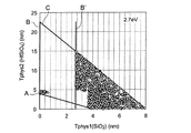
La 2 O 3 層
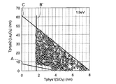
また、high−k層としてLa2O3層、low−k層としてSiO2層を選択して積層した場合の、様々なアシストレベルにおいて、本発明の一実施形態で定義したトンネル絶縁膜に求められるスペックを満たす物理膜厚の範囲を図19A乃至図19Nに示す。図19A乃至図19Nそれぞれ、La2O3層のアシストレベルが、0eV(無い場合)、0.1eV、0.3eV、0.5eV、0.7eV、0.9eV、1.1eV、1.3eV、1.5eV、1.7eV、1.9eV、2.1eV、2.3eV、2.5eVの場合の図である。そして、これらのアシストレベルと、トンネル絶縁膜のEOTとの関係を図20に示す。図20からわかるように、high−k層としてLa2O3層を選択した場合の、アシストレベルは0.1eV以上、1.9eV未満であることが好ましい。なお、アシストレベルがある場合には、そのlow−k層の層厚(直線Bと横軸との交点の値)を、アシストレベルが無い場合に必要なlow−k層の層厚(直線B’と横軸との交点の値)よりも薄くすることができる(図19C乃至図19J)。
La 2 O 3 layer also, La 2 O 3 layer as the high-k layer, when laminated to select the SiO 2 layer as a low-k layer, at various assist level, defined in an embodiment of the present invention The range of the physical film thickness that satisfies the specifications required for the tunnel insulating film is shown in FIGS. 19A to 19N. 19A to 19N, the assist levels of the La 2 O 3 layer are 0 eV (when none), 0.1 eV, 0.3 eV, 0.5 eV, 0.7 eV, 0.9 eV, 1.1 eV, 1.3 eV, respectively. , 1.5 eV, 1.7 eV, 1.9 eV, 2.1 eV, 2.3 eV, 2.5 eV. FIG. 20 shows the relationship between these assist levels and the EOT of the tunnel insulating film. As can be seen from FIG. 20, when the La 2 O 3 layer is selected as the high-k layer, the assist level is preferably 0.1 eV or more and less than 1.9 eV. When there is an assist level, the layer thickness of the low-k layer (the value of the intersection of the straight line B and the horizontal axis) is set to the layer thickness of the low-k layer (straight line B) when there is no assist level. (The value of the intersection point between 'and the horizontal axis) can be made thinner (FIGS. 19C to 19J).
この例では、low−k層としてSiO2を用いたが、SiN(窒化シリコン)はLa2O3層より誘電率が低いので、SiO2層と同様に、La2O3層に対してlow−k層として用いることができる。上述の説明ではlow−k層がSiO2層でhigh−k層がLa2O3層であったが、low−k層が酸化シリコン層であって、high−k層が酸化ランタン(LaO)層である場合でもアシストレベルが上述の範囲であれば同様の範囲で同様の効果を得ることができる。
In this example, SiO 2 is used as the low-k layer, since a lower SiN (silicon nitride) is the dielectric constant than La 2 O 3 layer, as in the SiO 2 layer,
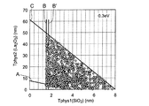
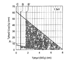
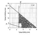
HfSiO層
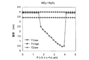
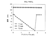
また、high−k層としてHfSiO4層、low−k層としてSiO2層を選択して積層した場合の、様々なアシストレベルにおいて、本発明の一実施形態で定義したトンネル絶縁膜に求められるスペックを満たす物理膜厚の範囲を図21A乃至図21Sに示す。図21A乃至図21Sはそれぞれ、HfSiO4層のアシストレベルが、0eV(無い場合)、0.1eV、0.3eV、0.5eV、0.7eV、0.9eV、1.1eV、1.3eV、1.5eV、1.7eV、1.9eV、2.1eV、2.3eV、2.5eV、2.7eV、2.9eV、3.1eV、3.3eV、3.5eVの場合の図である。そして、これらのアシストレベルと、トンネル絶縁膜のEOTとの関係を図22に示す。図22からわかるように、high−k層としてHfSiO4層を選択した場合の、アシストレベルは0.1eVより大きく、2.9eV以下であることが好ましい。なお、アシストレベルがある場合には、そのlow−k層の層厚(直線Bと横軸との交点の値)を、アシストレベルが無い場合に必要なlow−k層の層厚(直線B’と横軸との交点の値)よりも薄くすることができる(図21C乃至図21O)。また、HfSiO4は、アシストレベルが無い場合、SiO2層の層厚は2.7nmが必要であるが(図21A)、HfSiO4に0.3eV以上に深いアシストレベルがあれば、SiO2層が無くても、つまりHfSiO4の単層でもトンネル絶縁膜として用いることができる(図21C乃至図21O)。このとき、2.9eVよりも深いアシストレベルが有る場合は、EOTを可及的に薄くする効果は達成できない。また、low−k層としてSiO2を用いたが、SiNはHfSiO4層より誘電率が低いので、SiO2層と同様に、HfSiO4層に対してlow−k層として用いることができる。上述の説明ではlow−k層がSiO2層であって、high−k層がHfSiO4層であったが、low−k層が酸化シリコン層であって、high−k層がハフニウムシリケート(HfSiO)層である場合でもアシストレベルが上述の範囲であれば同様の範囲で同様の効果を得ることができる。
The tunnel insulating film defined in one embodiment of the present invention is required at various assist levels when the HfSiO layer and the HfSiO 4 layer as the high-k layer and the SiO 2 layer as the low-k layer are selected and laminated. The range of the physical film thickness that satisfies the required specifications is shown in FIGS. 21A to 21S. In FIGS. 21A to 21S, the assist levels of the HfSiO 4 layers are 0 eV (in the absence), 0.1 eV, 0.3 eV, 0.5 eV, 0.7 eV, 0.9 eV, 1.1 eV, 1.3 eV, It is a figure in the case of 1.5eV, 1.7eV, 1.9eV, 2.1eV, 2.3eV, 2.5eV, 2.7eV, 2.9eV, 3.1eV, 3.3eV, 3.5eV. FIG. 22 shows the relationship between these assist levels and the EOT of the tunnel insulating film. As can be seen from FIG. 22, when the HfSiO 4 layer is selected as the high-k layer, the assist level is preferably greater than 0.1 eV and less than or equal to 2.9 eV. When there is an assist level, the layer thickness of the low-k layer (the value of the intersection of the straight line B and the horizontal axis) is set to the layer thickness of the low-k layer (straight line B) when there is no assist level. (The value of the intersection point between 'and the horizontal axis) can be made thinner (FIGS. 21C to 21O). In the case where HfSiO 4 has no assist level, the layer thickness of the SiO 2 layer needs to be 2.7 nm (FIG. 21A), but if HfSiO 4 has an assist level deeper than 0.3 eV, the SiO 2 layer Even if there is no film, that is, even a single layer of HfSiO 4 can be used as a tunnel insulating film (FIGS. 21C to 21O). At this time, if there is an assist level deeper than 2.9 eV, the effect of making the EOT as thin as possible cannot be achieved. Although SiO 2 was used as the low-k layer, SiN has a lower dielectric constant than HfSiO 4 layer, similarly to the SiO 2 layer, can be used as the low-k layer with respect HfSiO 4 layer. In the above description, the low-k layer is an SiO 2 layer and the high-k layer is an HfSiO 4 layer. However, the low-k layer is a silicon oxide layer, and the high-k layer is a hafnium silicate (HfSiO The same effect can be obtained in the same range as long as the assist level is in the above-described range even in the case of a layer.
LaAlO層
また、high−k層としてLaAlO3層、low−k層としてSiO2層を選択して積層した場合の、様々なアシストレベルにおいて、本発明の一実施形態で定義したトンネル絶縁膜に求められるスペックを満たす物理膜厚の範囲を図23A乃至図23Nに示す。図23A乃至図23Nはそれぞれ、LaAlO3層のアシストレベルが、0eV(無い場合)0.1eV、0.3eV、0.5eV、0.7eV、0.9eV、1.1eV、1.3eV、1.5eV、1.7eV、1.9eV、2.1eV、2.3eV、2.5eVの場合の図である。そして、これらのアシストレベルと、トンネル絶縁膜のEOTとの関係を図24に示す。図24からわかるように、high−k層としてLaAlO3層を選択した場合の、アシストレベルは0eVより大きく、1.9eV未満であることが好ましい。なお、アシストレベルがある場合には、そのlow−k層の層厚(直線Bと横軸との交点の値)を、アシストレベルが無い場合に必要なlow−k層の層厚(直線B’と横軸との交点の値)よりも薄くすることができる(図23B乃至図23J)。この例では、low−k層としてSiO2を用いたが、SiN(窒化シリコン)はLaAlO3層より誘電率が低いので、SiO2層と同様に、LaAlO3層に対してlow−k層として用いることができる。上述の説明ではlow−k層がSiO2層であって、high−k層がLaAlO3層であったが、low−k層が酸化シリコン層であってhigh−k層がランタンアルミネート(LaAlO)層である場合でもアシストレベルが上述の範囲であれば同様の範囲で同様の効果を得ることができる。
A LaAlO layer , a LaAlO 3 layer as a high-k layer, and a SiO 2 layer as a low-k layer are selected and laminated at various assist levels, and the tunnel insulating film defined in one embodiment of the present invention is required. The range of the physical film thickness that satisfies the required specifications is shown in FIGS. 23A to 23N. In FIGS. 23A to 23N, the LaAlO 3 layer has an assist level of 0 eV (in the absence) 0.1 eV, 0.3 eV, 0.5 eV, 0.7 eV, 0.9 eV, 1.1 eV, 1.3 eV, 5eV, 1.7eV, 1.9eV, 2.1eV, 2.3eV, 2.5eV. FIG. 24 shows the relationship between these assist levels and the EOT of the tunnel insulating film. As can be seen from FIG. 24, when the LaAlO 3 layer is selected as the high-k layer, the assist level is preferably greater than 0 eV and less than 1.9 eV. When there is an assist level, the layer thickness of the low-k layer (the value of the intersection of the straight line B and the horizontal axis) is set to the layer thickness of the low-k layer (straight line B) when there is no assist level. (The value of the intersection point of 'and the horizontal axis) (Figs. 23B to 23J). In this example, SiO 2 is used as the low-k layer, SiN (silicon nitride) so has a lower dielectric constant than LaAlO 3 layers, similarly to the SiO 2 layer, as the low-k layer with respect LaAlO 3 layers Can be used. In the above description, the low-k layer is a SiO 2 layer and the high-k layer is a LaAlO 3 layer. However, the low-k layer is a silicon oxide layer and the high-k layer is a lanthanum aluminate (LaAlO 3). The same effect can be obtained in the same range as long as the assist level is in the above-described range even in the case of a layer.
HfAlO層
また、high−k層としてHf2Al2O7((HfO2)2/3(Al2O3)1/3)層、low−k層としてSiO2層を選択して積層した場合の、様々なアシストレベルにおいて、本発明の一実施形態で定義したトンネル絶縁膜に求められるスペックを満たす物理膜厚の範囲を図25A乃至図25Oに示す。図25A乃至図25Oはそれぞれ、Hf2Al2O7層のアシストレベルが、0eV(無い場合)、0.1eV、0.3eV、0.5eV、0.7eV、0.9eV、1.1eV、1.3eV、1.5eV、1.7eV、1.9eV、2.1eV、2.3eV、2.5eV、2.7eVの場合の図である。そして、これらのアシストレベルと、トンネル絶縁膜のEOTとの関係を図26に示す。図26からわかるように、high−k層としてHf2Al2O7層を選択した場合の、アシストレベルは0.1eVより大きく、2.1eV以下であることが好ましい。なお、Hf2Al2O7層にアシストレベルがある場合には、そのlow−k層の層厚(直線Bと横軸との交点の値)を、アシストレベルが無い場合に必要なlow−k層の層厚(直線B’と横軸との交点の値)よりも薄くすることができる(図25C乃至図25K)。また、Hf2Al2O7層は、1.5eV以上1.7eV以下にアシストレベルがあれば、SiO2層が無くても、つまりHf2Al2O7の単層としてトンネル絶縁膜に用いることができる(図25J乃至図25K)。しかし、Hf2Al2O7層は、2.1eV以上2.7eVにアシストレベルがある場合は、EOTを可及的に薄くする効果は達成できない。なお、low−k層としてSiO2を用いたが、SiN(窒化シリコン)はHf2Al2O7層より誘電率が低いので、SiO2層と同様に、Hf2Al2O7層に対してlow−k層として用いることができる。上述の説明ではlow−k層がSiO2層であって、high−k層がHf2Al2O7層であったが、low−k層が酸化シリコン層であって、high−k層がハフニウムアルミネート(HfAlO)層である場合でもアシストレベルが上述の範囲であれば同様の範囲で同様の効果を得ることができる。
HfAlO layer also, Hf 2 Al 2 O 7 ( (HfO 2) 2/3 (Al 2 O 3) 1/3) as the high-k layer layer, when laminated to select the SiO 2 layer as a low-k layer 25A to 25O show ranges of physical film thicknesses that satisfy the specifications required for the tunnel insulating film defined in one embodiment of the present invention at various assist levels. In FIGS. 25A to 25O, the assist levels of the Hf 2 Al 2 O 7 layer are 0 eV (in the absence), 0.1 eV, 0.3 eV, 0.5 eV, 0.7 eV, 0.9 eV, 1.1 eV, It is a figure in the case of 1.3eV, 1.5eV, 1.7eV, 1.9eV, 2.1eV, 2.3eV, 2.5eV, 2.7eV. FIG. 26 shows the relationship between these assist levels and the tunnel insulating film EOT. As can be seen from FIG. 26, when the Hf 2 Al 2 O 7 layer is selected as the high-k layer, the assist level is preferably greater than 0.1 eV and less than or equal to 2.1 eV. If the Hf 2 Al 2 O 7 layer has an assist level, the layer thickness of the low-k layer (the value of the intersection of the straight line B and the horizontal axis) is set to the low− level required when there is no assist level. It can be made thinner than the layer thickness of k layer (the value of the intersection of the straight line B ′ and the horizontal axis) (FIGS. 25C to 25K). Further, the Hf 2 Al 2 O 7 layer is used as a tunnel insulating film even if there is no SiO 2 layer, that is, as a single layer of Hf 2 Al 2 O 7 if there is an assist level of 1.5 eV to 1.7 eV. (FIGS. 25J to 25K). However, when the Hf 2 Al 2 O 7 layer has an assist level of 2.1 eV or more and 2.7 eV, the effect of making the EOT as thin as possible cannot be achieved. Although SiO 2 was used as the low-k layer, SiN (silicon nitride) has a lower dielectric constant than the Hf 2 Al 2 O 7 layer, so that the Hf 2 Al 2 O 7 layer is similar to the SiO 2 layer. Can be used as a low-k layer. In the above description, the low-k layer is an SiO 2 layer and the high-k layer is an Hf 2 Al 2 O 7 layer. However, the low-k layer is a silicon oxide layer, and the high-k layer is Even in the case of a hafnium aluminate (HfAlO) layer, the same effect can be obtained in the same range as long as the assist level is in the above range.
LaHfO層
また、high−k層としてLa2Hf2O7層、low−k層としてSiO2層を選択して積層した場合の、様々なアシストレベルにおいて、本発明の一実施形態で定義したトンネル絶縁膜に求められるスペックを満たす物理膜厚の範囲を図27A乃至図27Mに示す。図27a乃至図27Mはそれぞれ、La2Hf2O7層のアシストレベルが、0eV(無い場合)、0.1eV、0.3eV、0.5eV、0.7eV、0.9eV、1.1eV、1.3eV、1.5eV、1.7eV、1.9eV、2.1eV、2.3eVの場合の図である。そして、これらのアシストレベルと、トンネル絶縁膜のEOTとの関係を図28に示す。図28からわかるように、high−k層としてLa2Hf2O7層を選択した場合の、アシストレベルは0.1eV以上1.7eV以下であることが好ましい。なお、アシストレベルがある場合には、そのlow−k層の層厚(直線Bと横軸との交点の値)を、アシストレベルが無い場合に必要なlow−k層の層厚(直線B’と横軸との交点の値)よりも薄くすることができる(図27C乃至図27I)。この例では、low−k層としてSiO2を用いたが、SiN(窒化シリコン)はLa2Hf2O7層より誘電率が低いので、SiO2層と同様に、La2Hf2O7層に対してlow−k層として用いることができる。上述の説明ではlow−k層がSiO2層であって、high−k層がLa2Hf2O7層であったが、low−k層が酸化シリコン層であって、high−k層がランタンハフネート(LaHfO)層である場合でもアシストレベルが上述の範囲であれば同様の範囲で同様の効果を得ることができる。
A tunnel defined in one embodiment of the present invention at various assist levels when a LaHfO layer , a La 2 Hf 2 O 7 layer as a high-k layer, and a SiO 2 layer as a low-k layer are selected and laminated. 27A to 27M show ranges of physical film thicknesses that satisfy specifications required for insulating films. 27a to 27M, the assist levels of the La 2 Hf 2 O 7 layer are 0 eV (in the absence), 0.1 eV, 0.3 eV, 0.5 eV, 0.7 eV, 0.9 eV, 1.1 eV, It is a figure in the case of 1.3eV, 1.5eV, 1.7eV, 1.9eV, 2.1eV, 2.3eV. FIG. 28 shows the relationship between these assist levels and the EOT of the tunnel insulating film. As can be seen from FIG. 28, when the La 2 Hf 2 O 7 layer is selected as the high-k layer, the assist level is preferably 0.1 eV or more and 1.7 eV or less. When there is an assist level, the layer thickness of the low-k layer (the value of the intersection of the straight line B and the horizontal axis) is set to the layer thickness of the low-k layer (straight line B) when there is no assist level. (The value of the intersection point between 'and the horizontal axis). In this example, SiO 2 is used as the low-k layer, since SiN (silicon nitride) has a lower dielectric constant than La 2 Hf 2 O 7 layer, as in the SiO 2 layer, La 2 Hf 2 O 7 layer Can be used as a low-k layer. In the above description, the low-k layer is a SiO 2 layer and the high-k layer is a La 2 Hf 2 O 7 layer. However, the low-k layer is a silicon oxide layer, and the high-k layer is Even in the case of a lanthanum hafnate (LaHfO) layer, the same effect can be obtained in the same range as long as the assist level is in the above range.
SiN層
また、SiN(窒化シリコン)は、SiO2の誘電率に較べてほぼ二倍と高いので、SiNはSiO2に対してhigh−k絶縁層として機能する。そこで、high−k層としてSiN層、low−k層としてSiO2層を選択して積層した場合の、様々なアシストレベルにおいて、本発明の一実施形態で定義したトンネル絶縁膜に求められるスペックを満たす物理膜厚の範囲を図29A乃至図29Kに示す。図29A乃至図29Kはそれぞれ、SiN層のアシストレベルが、0eV(無い場合)、0.1eV、0.3eV、0.5eV、0.7eV、0.9eV、1.1eV、1.3eV、1.5eV、1.7eV、1.9eVの場合の図である。そして、これらのアシストレベルと、トンネル絶縁膜のEOTとの関係を図30に示す。図30からわかるように、high−k層としてSiN層を選択した場合、EOTを薄くするための適切なアシストレベルは存在しない。しかし、アシストレベルを形成することによって、低い電界で消去特性のスペックを満たすので、消去効率を上げることができる。
SiN layer also, SiN (silicon nitride), since almost twice as high compared to the dielectric constant of SiO 2, SiN functions as a high-k dielectric layer with respect to SiO 2. Therefore, the specifications required for the tunnel insulating film defined in one embodiment of the present invention at various assist levels when an SiN layer as a high-k layer and an SiO 2 layer as a low-k layer are selected and laminated. The range of the physical film thickness to be satisfied is shown in FIGS. 29A to 29K. In FIGS. 29A to 29K, the SiN layer assist levels are 0 eV (in the absence), 0.1 eV, 0.3 eV, 0.5 eV, 0.7 eV, 0.9 eV, 1.1 eV, 1.3 eV, 1 It is a figure in case of .5eV, 1.7eV, 1.9eV. FIG. 30 shows the relationship between these assist levels and the EOT of the tunnel insulating film. As can be seen from FIG. 30, when the SiN layer is selected as the high-k layer, there is no appropriate assist level for reducing the EOT. However, by forming the assist level, the specification of the erasing characteristic is satisfied with a low electric field, so that the erasing efficiency can be increased.
Ta 2 O 5 層
また、high−k層としてTa2O5層、low−k層としてSiO2層を選択して積層した場合の、様々なアシストレベルにおいて、本発明の一実施形態で定義したトンネル絶縁膜に求められるスペックを満たす物理膜厚の範囲を図31A乃至図31Jに示す。図31A乃至図31Jはそれぞれ、Ta2O5層のアシストレベルが、0eV(無い場合)、0.1eV、0.3eV、0.5eV、0.7eV、0.9eV、1.1eV、1.3eV、1.5eV、1.7eVの場合の図である。そして、これらのアシストレベルと、トンネル絶縁膜のEOTとの関係を図32に示す。図32からわかるように、high−k層としてTa2O5層を選択した場合の、アシストレベルは0eVより大きく1.3eV以下であることが好ましい。なお、アシストレベルがある場合には、そのlow−k層の層厚(直線Bと横軸との交点の値)を、アシストレベルが無い場合に必要なlow−k層の層厚(直線B’と横軸との交点の値)よりも薄くすることができる(図31B乃至図31F)。この例では、low−k層としてSiO2を用いたが、SiN(窒化シリコン)はTa2O5層より誘電率が低いので、SiO2層と同様に、Ta2O5層に対してlow−k層として用いることができる。上述の説明ではlow−k層がSiO2層であって、high−k層がTa2O5層であったが、low−k層が酸化シリコン層であって、high−k層がタンタルオキサイド(TaO)層である場合でもアシストレベルが上述の範囲であれば同様の範囲で同様の効果を得ることができる。
Ta 2 O 5 layer also, Ta 2 O 5 layer as the high-k layer, when laminated to select the SiO 2 layer as a low-k layer, at various assist level, defined in an embodiment of the present invention The range of the physical film thickness that satisfies the specifications required for the tunnel insulating film is shown in FIGS. 31A to 31J. 31A to 31J, the assist levels of the Ta 2 O 5 layer are 0 eV (when none), 0.1 eV, 0.3 eV, 0.5 eV, 0.7 eV, 0.9 eV, 1.1 eV, 1. It is a figure in the case of 3 eV, 1.5 eV, and 1.7 eV. FIG. 32 shows the relationship between these assist levels and the EOT of the tunnel insulating film. As can be seen from FIG. 32, when the Ta 2 O 5 layer is selected as the high-k layer, the assist level is preferably greater than 0 eV and not greater than 1.3 eV. When there is an assist level, the layer thickness of the low-k layer (the value of the intersection of the straight line B and the horizontal axis) is set to the layer thickness of the low-k layer (straight line B) when there is no assist level. (The value of the intersection point between 'and the horizontal axis) can be made thinner (FIGS. 31B to 31F). In this example, SiO 2 is used as the low-k layer, but SiN (silicon nitride) has a lower dielectric constant than the Ta 2 O 5 layer, so that it is low relative to the Ta 2 O 5 layer, similar to the SiO 2 layer. It can be used as a -k layer. In the above description, the low-k layer is a SiO 2 layer and the high-k layer is a Ta 2 O 5 layer, but the low-k layer is a silicon oxide layer and the high-k layer is a tantalum oxide. Even in the case of the (TaO) layer, if the assist level is in the above range, the same effect can be obtained in the same range.
図13A−図13P、図17A−図17Z、図19A−図19N、図21A−図21S、図23A−図23N、図25A−図25O、図27A−図27M、図29A−図29K、図31A−図31Jにおいて、層厚の範囲の中に点が打たれていない領域が存在するが、そこはホールがエネルギーを放出しながらトラップされる領域を示しており、他の点の打たれている領域と同様にトンネル絶縁膜としてのスペックを満たす。 13A-13P, 17A-17Z, 19A-19N, 21A-21S, 23A-23N, 25A-25O, 27A-27M, 29A-29K, 31A -In Fig. 31J, there is an undotted region in the layer thickness range, which shows the region where holes are trapped while releasing energy, and other points are struck. It satisfies the specifications as a tunnel insulating film as well as the region.
また、図14、図18、図20、図22、図24、図26、図28、図30、および図32は、EOTを薄くするためのアシストレベルの適切な範囲も示している。各high−k層に対してこれらの適切な範囲を図33A、33Bに示す。すなわち、図33Aは、アシストレベルのある積層構造において、各high−k絶縁層の単層膜よりも効果のあるアシストレベルの範囲を示しているグラフであり、図33Bは、そのアシストレベルの範囲と最小のEOTを示す表である。図33Bからわかるように、トンネル絶縁膜のEOTは、その下限がhigh−k層がTa2O5層である場合の1.02nmとなる。なお、上限は、第1実施形態で説明したように5nmとなる。すなわち、トンネル絶縁膜のEOTは、1.02nm〜5nmの範囲にあればよい。 FIGS. 14, 18, 20, 22, 24, 26, 28, 30, and 32 also show appropriate ranges of assist levels for reducing EOT. These appropriate ranges are shown in FIGS. 33A and 33B for each high-k layer. That is, FIG. 33A is a graph showing a range of assist levels that are more effective than a single-layer film of each high-k insulating layer in a laminated structure with assist levels, and FIG. 33B shows the range of assist levels. And a table showing the minimum EOT. As can be seen from FIG. 33B, the lower limit of the EOT of the tunnel insulating film is 1.02 nm when the high-k layer is a Ta 2 O 5 layer. The upper limit is 5 nm as described in the first embodiment. That is, the EOT of the tunnel insulating film may be in the range of 1.02 nm to 5 nm.
また、各種のhigh−k層とSiO2層を積層したトンネル絶縁膜にアシストレベルが有る場合と、無い場合の、EOTの最小値を比較した結果を図34A、34Bに示す。図34A、34Bからわかるように、アシストレベルが有る場合の方が、無い場合に比べてEOTを薄膜化することができる。 Further, FIGS. 34A and 34B show the results of comparing the minimum values of EOT when the tunnel insulating film in which various high-k layers and SiO 2 layers are laminated has the assist level and when there is no assist level. As can be seen from FIGS. 34A and 34B, the EOT can be made thinner when the assist level is present than when the assist level is absent.
なお、上述したhigh−k材料以外でも、誘電率およびΔEVが、上述したhigh−k層と同じくらいか、あるいはこれらの層の間にある場合には、これらの材料を、本発明の一実施形態のhigh−k層として用いることができる。この場合、適正な物理層厚の範囲があり、その範囲はこれまでの議論から、計算によって正確に見積もることもできるし、上述した各high−k層のデータから、内挿あるいは外挿することによっても見積もることも可能である。 Even in non-high-k materials described above, dielectric constant and Delta] E V is either much as high-k layer described above, or in some cases between these layers, these materials, the present invention one It can be used as the high-k layer of the embodiment. In this case, there is an appropriate range of the physical layer thickness, and the range can be accurately estimated by calculation from the discussion so far, or can be interpolated or extrapolated from the data of each high-k layer described above. Can also be estimated.
また、low−k絶縁層として、SiO2の場合を示したが、低誘電率であれば、SiN、SiONなどの窒化膜、酸窒化膜、あるいはそれを含む絶縁膜でも、同様の効果がある。なお、TiO2では、アシストレベルの有無にかかわらず、本発明の一実施形態で定義したトンネル絶縁膜のスペックでは、これを満たす膜厚の範囲は無かった。 In addition, although the case of SiO 2 is shown as the low-k insulating layer, a similar effect can be obtained with a nitride film such as SiN or SiON, an oxynitride film, or an insulating film including the same if the dielectric constant is low. . In TiO 2 , regardless of the presence or absence of the assist level, the specification of the tunnel insulating film defined in the embodiment of the present invention has no film thickness range that satisfies this.
high−k層およびlow−k層を積層した場合、基本的には、以下のように一般化できる。high−k層がHfO2層、low−k層がSiO2層の場合であり、トンネル絶縁膜として求められるホールのリーク電流のスペックをEoxが3MV/cmの低電界では1.0×10−16A/cm2以下、13MV/cmの高電界では1.0×10−5A/cm2以上としたが、誘電率が異なる層であれば、基本的には考え方は全く同じであり、同様の効果が得られる。電荷保持状態で要求されるスペックが、電界Elowにおいてリーク電流がJlow以下とする。そのとき、アシストレベルのあるlow−k層、high−k層の各単層においてリーク電流をJlow以下にするのに必要な物理膜厚をそれぞれT1,low、T2,lowとし、low−k層およびhigh−k層を積層したときのそれぞれの物理層厚をT1、T2とすると、
T2=−(T2,low/T1,low)×T1+T2,low (13)
を満足する。これは、上述の、図10、図13A−図13P、図17A−図17Z、図19A−図19N、図21A−図21S、図23A−図23N、図25A−図25O、図27A−図27M、図29A−図29K、図31A−図31Jにおいて直線Aに対応する式である。T1,lowは直線Aと横軸との交点の値となり、T2,lowは直線Aと縦軸との交点の値となる。したがって、low−k層がSiO2の場合、T2,lowは4nmになる。
When the high-k layer and the low-k layer are stacked, the generalization can be made as follows. high-k layer is HfO 2 layer, low-k layer is a case of the SiO 2 layer, tunnel Eox specifications of the leakage current of holes required as an insulating film is 3 MV / cm in a low electric field 1.0 × in 10 - In a high electric field of 16 A / cm 2 or less and 13 MV / cm, it was 1.0 × 10 −5 A / cm 2 or more. However, if the layers have different dielectric constants, the idea is basically the same. Similar effects can be obtained. The specification required in the charge holding state is that the leakage current is equal to or lower than J low at the electric field E low . At that time, the physical film thicknesses required to make the leakage current equal to or less than J low in each of the low-k layer and the high-k layer having the assist level are T 1, low and T 2, low , respectively. If each physical layer thickness when the laminated -k layer and high-k layer and T 1, T 2,
T 2 = − (T 2, low / T 1, low ) × T 1 + T 2, low (13)
Satisfied. This is described above with reference to FIGS. 10, 13A-13P, 17A-17Z, 19A-19N, 21A-21S, 23A-23N, 25A-25O, 27A-27M. 29A to 29K and FIGS. 31A to 31J are equations corresponding to the straight line A. T1 , low is the value of the intersection of the straight line A and the horizontal axis, and T2 , low is the value of the intersection of the straight line A and the vertical axis. Therefore, when the low-k layer is SiO 2 , T 2 and low are 4 nm.
そして、書込に要求されるスペックが、電界Ehighにおいてリーク電流がJhigh以上とする。そのときに最低限必要なlow−k層の膜厚をT1,highとすると、
T1=T1,high (14)
となる。これは、図9に示す直線Bに対応する。
The specification required for writing is such that the leakage current is J high or more at the electric field E high . If the minimum required thickness of the low-k layer is T1 , high ,
T 1 = T 1, high (14)
It becomes. This corresponds to the straight line B shown in FIG.
なお、トンネル絶縁膜として機能するには、low−k層のトラップレベルφt1に制限があり、
0 ≦ φt1 ≦ Δφb + φt2 (15)
を満たすか、あるいはlow−k層にトラップがない必要がある。ここで、Δφbは
Δφb= φb1−φb2 (16)
と定義した。(15)式を満たさないと、低電界でリーク電流が高くなり、電荷保持ができない。なお、φb1およびφb2はそれぞれシリコン基板のフェルミレベルEFに対するlow−k層およびhigh−k層のホールのバリアハイトを表す。
In order to function as a tunnel insulating film, the trap level φ t1 of the low-k layer is limited,
0 ≦ φ t1 ≦ Δφ b + φ t2 (15)
Or there is no trap in the low-k layer. Here, [Delta] [phi b is Δφ b = φ b1 -φ b2 ( 16)
Defined. If the equation (15) is not satisfied, the leakage current increases with a low electric field, and charge cannot be retained. Note that represents the barrier height of the hole of the low-k layer and the high-k layer with respect to phi b1 and phi b2 Fermi level E F of each silicon substrate.
こうして、アシストレベルと、トンネル絶縁膜として必要な各絶縁層の膜厚の範囲の関係は、(13)式〜(16)式から決定される。 Thus, the relationship between the assist level and the range of the film thickness of each insulating layer required as the tunnel insulating film is determined from the equations (13) to (16).
様々なアシストレベルに対する、high−k層とlow−k層の層厚の範囲をまとめたものを、図35乃至図43に示す。図35は、high−k層としてHfO2層を選択し、low−k層としてSiO2層を選択した場合のアシストレベルと、T1,low、T1,high、T2,lowとの関係を示している。図36は、high−k層としてAl2O3層を選択し、low−k層としてSiO2層を選択した場合のアシストレベルと、T1,low、T1,high、T2,lowとの関係を示している。図37は、high−k層としてLa2O3層を選択し、low−k層としてSiO2層を選択した場合のアシストレベルと、T1,low、T1,high、T2,lowとの関係を示している。図38は、high−k層としてHfSiO4層を選択し、low−k層としてSiO2層を選択した場合のアシストレベルと、T1,low、T1,high、T2,lowとの関係を示している。図39は、high−k層としてLaAlO3層を選択し、low−k層としてSiO2層を選択した場合のアシストレベルと、T1,low、T1,high、T2,lowとの関係を示している。図40は、high−k層としてHf2Al2O7層を選択し、low−k層としてSiO2層を選択した場合のアシストレベルと、T1,low、T1,high、T2,lowとの関係を示している。図41は、high−k層としてLa2Hf2O7層を選択し、low−k層としてSiO2層を選択した場合のアシストレベルと、T1,low、T1,high、T2,lowとの関係を示している。図42は、high−k層としてSiN層を選択し、low−k層としてSiO2層を選択した場合のアシストレベルと、T1,low、T1,high、T2,lowとの関係を示している。図43は、high−k層としてTa2O5層を選択し、low−k層としてSiO2層を選択した場合のアシストレベルと、T1,low、T1,high、T2,lowとの関係を示している。これらからトンネル絶縁膜のスペックを満たす、high−k層の種類(あるいはバリアハイトと誘電率)、low−k層と積層にしたときの層厚の範囲、アシストレベルが限定される。図35乃至図43からわかるように、T1,lowおよびT2,lowは材料によって変わるが、アシストレベルによってはほとんど変化せず、T1,highは材料およびアシストレベルによって変化することがわかる。 FIG. 35 to FIG. 43 show a summary of the range of the layer thicknesses of the high-k layer and the low-k layer for various assist levels. Figure 35 selects the HfO 2 layer as the high-k layer, and the assist level when selecting an SiO 2 layer as a low-k layer, T 1, low, T 1 , high, relationship between T 2, low Is shown. FIG. 36 shows the assist level when the Al 2 O 3 layer is selected as the high-k layer and the SiO 2 layer is selected as the low-k layer, and T 1, low , T 1, high , T 2, low Shows the relationship. FIG. 37 shows the assist level when the La 2 O 3 layer is selected as the high-k layer and the SiO 2 layer is selected as the low-k layer, and T 1, low , T 1, high , T 2, low Shows the relationship. Figure 38 selects the HfSiO 4 layer as a high-k layer, and the assist level when selecting an SiO 2 layer as a low-k layer, T 1, low, T 1 , high, relationship between T 2, low Is shown. FIG. 39 shows the relationship between the assist level and the T 1, low , T 1, high , T 2, low when the LaAlO 3 layer is selected as the high-k layer and the SiO 2 layer is selected as the low-k layer. Is shown. FIG. 40 shows an assist level when the Hf 2 Al 2 O 7 layer is selected as the high-k layer and the SiO 2 layer is selected as the low-k layer, and T 1, low , T 1, high , T 2 The relationship with low is shown. FIG. 41 shows the assist level when the La 2 Hf 2 O 7 layer is selected as the high-k layer and the SiO 2 layer is selected as the low-k layer, and T 1, low , T 1, high , T 2 The relationship with low is shown. Figure 42 selects the SiN layer as a high-k layer, and the assist level when selecting an SiO 2 layer as a low-k layer, T 1, low, T 1 , high, the relationship between T 2, low Show. FIG. 43 shows the assist level when the Ta 2 O 5 layer is selected as the high-k layer and the SiO 2 layer is selected as the low-k layer, and T 1, low , T 1, high , T 2, low Shows the relationship. Accordingly, the type of high-k layer (or barrier height and dielectric constant) that satisfies the specifications of the tunnel insulating film, the range of the layer thickness when laminated with the low-k layer, and the assist level are limited. As can be seen from FIGS. 35 to 43, although T 1, low and T 2, low vary depending on the material, they hardly change depending on the assist level, and T 1, high varies depending on the material and the assist level.
上記(13)式(例えば図10における直線Aを示す式)、(14)式(例えば図10における直線Bを示す式)と、high−k層とlow−k層とからなる積層絶縁膜のEOTの規定値(上記実施形態では、EOT=8nm)を示す式(例えば図10における直線Cを示す式)、および各材料におけるアシストレベルの好適な範囲によって、high−k層およびlow−k層のそれぞれの好適な物理膜厚の範囲を求めることができる。なお、high−k層とlow−k層とからなる積層絶縁膜のEOTtotalの規定値(上記実施形態では、EOT=8nm)を示す式は、low−k層およびhigh−k層のそれぞれの誘電率をε1,ε2、物理膜厚をT1、T2、SiO2の誘電率をεoxとすると、
EOTtotal= T1×εox/ε1+ T2×εox/ε2= 8 (nm) (17)
と表される。したがって、(13)式、(14)式、(17)式のよって囲まれる領域がhigh−k層およびlow−k層のそれぞれの好適な物理膜厚の領域となる。この領域は、各材料におけるアシストレベルの好適な範囲によって変わることになる。また、この領域は、次の3つの不等式を満たす領域と同等である。
T2≧−(T2,low/T1,low)×T1+T2,low
T1≧T1,high
T1×εox/ε1+ T2×εox/ε2≦ 8
そして、トンネル絶縁膜を最小にする膜厚は、T1が(14)式によって求まり、T2が(14)式を(13)に代入することにより、
T2=−(T2,low/T1,low)×T1,high+T2,low (18)
となる。
The above-described expression (13) (for example, an expression indicating the straight line A in FIG. 10), (14) (for example, an expression indicating the straight line B in FIG. 10), and a stacked insulating film composed of a high-k layer and a low-k layer A high-k layer and a low-k layer depending on an equation (for example, an equation showing a straight line C in FIG. 10) indicating a specified value of EOT (for example, an equation showing a straight line C in FIG. 10) and a suitable range of assist levels in each material. Each of the preferable ranges of the physical film thickness can be obtained. Note that the equation indicating the EOT total of the stacked insulating film composed of the high-k layer and the low-k layer (in the above embodiment, EOT = 8 nm) is expressed by the low-k layer and the high-k layer, respectively. When the dielectric constant is ε 1 , ε 2 , the physical film thickness is T 1 , T 2 , and the dielectric constant of SiO 2 is ε ox ,
EOT total = T 1 × ε ox / ε 1 + T 2 × ε ox / ε 2 = 8 (nm) (17)
It is expressed. Therefore, the regions surrounded by the equations (13), (14), and (17) are regions having suitable physical film thicknesses of the high-k layer and the low-k layer. This region will vary depending on the preferred range of assist levels for each material. This region is equivalent to a region that satisfies the following three inequalities.
T 2 ≧ − (T 2, low / T 1, low ) × T 1 + T 2, low
T 1 ≧ T 1, high
T 1 × ε ox / ε 1 + T 2 × ε ox / ε 2 ≦ 8
Then, the film thickness to minimize the tunnel insulating film, Motomari by T 1 is (14), by substituting T 2 is the (14) formula (13),
T 2 = − (T 2, low / T 1, low ) × T 1, high + T 2, low (18)
It becomes.
このように、どのようなhigh−k層でも、(13)、(14)、(17)、(18)式から、トンネル絶縁膜として求められるスペックを満たす、high−k層、low−k層からなる積層絶縁膜の、それぞれの膜厚や有効なアシストレベルを決定するのは容易である。 Thus, in any high-k layer, the high-k layer and the low-k layer satisfy the specifications required as a tunnel insulating film from the equations (13), (14), (17), and (18). It is easy to determine the respective film thicknesses and effective assist levels of the laminated insulating film.
(アシストレベルの分布について)
ホールのアシストレベルは、膜と水平方向に一様に存在している必要はない。図44(a)、44(b)にアシストレベルが部分的にある場合のトンネル絶縁膜の模式図を示す。このトンネル絶縁膜は、基板1上にlow−k層8と、アシストレベルのあるhigh−k層9とを積層して形成される。ここで、アシストレベルがある領域の割合をRとすると、無い領域の割合は1−Rとなる。そして、アシストレベルがある場合のリーク電流をJtat、無い場合のリーク電流をJ0とすると、膜全体を流れる電流Jは、
J=R×Jtat+(1−R)×J0 (19)
と表せる。低電界では、リーク電流はアシストレベルの有無によらないため、リーク電流は膜全体で低く抑えられる。一方で、高電界では、アシストレベルがあるとリーク電流が高くなるので、アシストレベルのある領域だけでリーク電流を高くできる。アシストレベルは、図44(a)、44(b)に示すように、例えば、膜の端より内側にアシストレベルを形成することができる。こうすることによって、電界集中して絶縁破壊が起こりやすい端を避けてリーク電流を高くできるため、膜の信頼性を高くすることができる。
(About assist level distribution)
The assist level of the hole does not need to exist uniformly in the horizontal direction with respect to the film. 44 (a) and 44 (b) are schematic views of the tunnel insulating film when the assist level is partially present. This tunnel insulating film is formed by laminating a low-
J = R × J tat + (1−R) × J 0 (19)
It can be expressed. In a low electric field, since the leakage current does not depend on the presence or absence of the assist level, the leakage current can be kept low throughout the film. On the other hand, in a high electric field, the leakage current increases when there is an assist level. Therefore, the leakage current can be increased only in a region having the assist level. As shown in FIGS. 44 (a) and 44 (b), for example, the assist level can be formed inside the end of the film. By doing so, the leakage current can be increased by avoiding the edge where the electric field is concentrated and the dielectric breakdown is likely to occur, so that the reliability of the film can be increased.
なお、high−k層(例えばHfO2層)に元々存在する欠陥、例えば、酸素が欠損してできた欠陥、いわゆる酸素欠損(oxygen vacancy)は、不安定であり、制御されていないため、本発明の一実施形態のアシストレベルと同じ機能は発揮しない。すなわち、本発明の一実施形態と同じ効果を得るには、本発明の一実施形態のように、トンネル絶縁膜として要求されるスペックを満たすような、最適な位置に充分な密度のアシストレベルが形成されるように元素を添加する必要がある。つまり、もともと欠陥の無い層、あるいは本質的に欠陥のある層に、意図的に形成したアシストレベルを形成する必要がある。それ故、必然的にそのような効果を持つ絶縁層は、添加される元素を含めて考えたとき、三元以上の元素からなる層となる。また、添加される元素は、添加する層を構成する格子を置換した位置でも良いし、添加する層を構成する格子間の位置でも良い。 It should be noted that defects originally present in the high-k layer (for example, HfO 2 layer), for example, defects formed by oxygen deficiency, so-called oxygen vacancy, are unstable and are not controlled. The same function as the assist level of one embodiment of the invention is not exhibited. That is, in order to obtain the same effect as that of the embodiment of the present invention, as in the embodiment of the present invention, an assist level having a sufficient density is provided at an optimal position that satisfies the specifications required for the tunnel insulating film. It is necessary to add elements so that they are formed. That is, it is necessary to form an intentionally formed assist level in a layer that is originally free from defects or in a layer that is essentially defective. Therefore, an insulating layer having such an effect inevitably becomes a layer composed of ternary or higher elements when including the added element. Further, the element to be added may be a position where the lattice constituting the layer to be added is replaced, or may be a position between the lattices constituting the layer to be added.
また、トンネル絶縁膜は、第1絶縁層(low−k層)と、第2絶縁層(high−k層)と、第3絶縁層とがこの順序で積層された積層構造を有しているとき、第3絶縁層は、第1絶縁層と同じ誘電率を有しているか或いは第1絶縁層の誘電率と第2絶縁層の誘電率との間の誘電率を有していることが好ましい。 The tunnel insulating film has a stacked structure in which a first insulating layer (low-k layer), a second insulating layer (high-k layer), and a third insulating layer are stacked in this order. In some cases, the third insulating layer has the same dielectric constant as the first insulating layer, or has a dielectric constant between the dielectric constant of the first insulating layer and the dielectric constant of the second insulating layer. preferable.
(第3実施形態)
次に、本発明の第3実施形態によるFG型不揮発性メモリの製造方法を、図45(a)乃至図46(d)を参照して説明する。図45(a)、図45(c)、図45(e)、図46(a)、図46(c)と、図451(b)、図45(d)、図45(f)、図46(b)、図46(d)とは、それぞれ直交する断面を表している。
(Third embodiment)
Next, a method of manufacturing the FG nonvolatile memory according to the third embodiment of the present invention will be described with reference to FIGS. 45 (a) to 46 (d). 45 (a), 45 (c), 45 (e), 46 (a), 46 (c), 451 (b), 45 (d), 45 (f), FIG. 46 (b) and FIG. 46 (d) each represent a cross section orthogonal to each other.
まず、図45(a)、45(b)に示すように、所望の不純物をドーピングしたp型シリコン基板1の表面に、上述の実施形態で説明したアシストレベルのあるトンネル絶縁膜22を形成する。例えば、750℃で水素と酸素を用いた燃焼酸化で表面を酸化し、SiO2層を形成後、ホールのアシストレベルが形成されたhigh−k膜、例えばRuを添加したHfO2層を形成し、アシストレベルのあるトンネル絶縁膜をCVDにより形成する。続いて、浮遊ゲート電極となる厚さ60nmのリンドープの結晶性シリコン層23をCVD(chemical vapor deposition)法を用いて堆積する。この結晶性シリコン層23上に例えばシリコン窒化膜からなるマスク材24を形成する。その後、レジストマスク(図示せず)を用いた反応性イオンエッチング(RIE(reactive ion etching))法により、マスク材24、浮遊ゲート電極23、トンネル絶縁膜22を順次エッチング加工し、シリコン基板1の表面を一部露出させる。更にシリコン基板1の露出した領域をエッチングして、深さ100nmの素子分離溝25を形成する。
First, as shown in FIGS. 45A and 45B, the
次に、図45(c)、45(d)に示すように、全面に素子分離用のシリコン酸化膜26を堆積して、素子分離溝25を完全に埋め込む。その後、表面部分のシリコン酸化膜26をCMP(chemical mechanical polishing)法で除去して、表面を平坦化する。このとき、マスク材であるシリコン窒化膜24の上面が露出する。
Next, as shown in FIGS. 45C and 45D, a
次に、露出したマスク材22を選択的にエッチング除去した後、シリコン酸化膜26の露出表面を希フッ酸溶液等でエッチング除去し、浮遊ゲート電極23の側壁面を一部露出させる。続いて、電極間絶縁膜27となる高誘電体膜を形成する。例えば、浮遊ゲート電極(リンドープの結晶性シリコン層)23上に、例えば、Al2O3、SiN、SiO2、La2O3、HfO2、TaO2、TiO2のうちの一つ、あるいはそれらの多層膜や混合した膜からなる電極間絶縁膜27を形成する(図45(e)、45(f))。
Next, the exposed
次に、図46(a)、46(b)に示すように、制御ゲート電極としてCVD法でリンドープのn+型多結晶シリコン層28を620℃で堆積して形成し、その上にタングステンシリサイド(WSi)層29を形成することにより、WSi層/多結晶Si層からなる2層構造の厚さ100nmの導電層を形成する。ここで、WSi層29は、W(CO)6を原料ガスとするCVD法を用いてWを堆積し、その後の熱工程で多結晶シリコン層をWSixに変換することにより形成する。なお、これらの膜の製造方法はここに示した方法に限らず、他の原料ガスを用いてもよい。また、CVD法以外の方法、例えば、ALD(Atomic Layer Deposition)法、スパッター法、蒸着法、レーザーアブレーション法、MBE法、またこれらの手法を組み合わせた成膜方法も可能である。多結晶Si層ではなく、金属でもかまわない。
Next, as shown in FIGS. 46A and 46B, a phosphorus-doped n + -type
その後、レジストマスク(図示せず)を用いたRIE法により、WSi層29、多結晶シリコン層28、電極間絶縁膜27、単結晶シリコンの浮遊ゲート電極23、トンネル絶縁膜22を順次エッチング加工して、ワード線方向のスリット部40を形成する。これにより、浮遊ゲート電極及び制御ゲート電極の形状が確定する。
Thereafter, the
最後に、図46(c)、46(d)に示すように、露出面に電極側壁酸化膜と呼ばれるシリコン酸化膜30を熱酸化法で形成後、イオン注入法を用いてn+型のソース/ドレイン拡散層31を形成する。更に、全面を覆うようにシリコン酸化膜などの層間絶縁膜32をCVD法で形成する。その後は、周知の方法で配線層等を形成して不揮発性メモリセルが完成する。
Finally, as shown in FIGS. 46 (c) and 46 (d), a
(第4実施形態)
次に、本発明の第4実施形態によるMONOS型不揮発性メモリの製造方法を、図47(a)乃至図48(d)を参照して説明する。図47(a)、図47(c)、図47(e)、図48(a)、図48(c)と、図47(b)、図47(d)、図47(f)、図48(b)、図48(d)とは、それぞれ直交する断面を表している。
(Fourth embodiment)
Next, a method of manufacturing the MONOS nonvolatile memory according to the fourth embodiment of the present invention will be described with reference to FIGS. 47 (a) to 48 (d). 47 (a), 47 (c), 47 (e), 48 (a), 48 (c), 47 (b), 47 (d), 47 (f), FIG. 48 (b) and FIG. 48 (d) each represent a cross section orthogonal to each other.
まず、図47(a)、47(b)に示すように、所望の不純物をドーピングしたp型シリコン基板1の表面に、上述の実施形態で説明したアシストレベルのあるトンネル絶縁膜33を形成する。例えば、750℃で水素と酸素を用いた燃焼酸化で表面を酸化し、SiO2層を形成後、CVDによりホールのアシストレベルが形成されたhigh−k膜、例えばRuを添加したHfO2層を形成する。続いて、電荷蓄積層となる厚さ60nmのシリコン窒化膜34をCVD法で堆積する。このとき使用するガスは、例えばジクロルシラン(SiH2Cl2)とアンモニア(NH3)、もしくはヘキサクロルジシラン(Si2Cl6)とアンモニア(NH3)を用いて行い、成膜温度は約450℃から800℃である。その後、レジストマスク(図示せず)を用いたRIE法により、電荷蓄積層であるシリコン窒化膜34、トンネル絶縁膜33を順次エッチング加工し、シリコン基板1の一部分を露出させる。さらにシリコン基板1の露出した領域をエッチングして、深さ100nmの素子分離溝25を形成する。
First, as shown in FIGS. 47A and 47B, the
次に、図47(c)、47(d)に示すように、全面に素子分離用のシリコン酸化膜26を堆積して、素子分離溝25を完全に埋め込む。その後、表面部分のシリコン酸化膜26をCMP法で除去して、表面を平坦化する。このとき、シリコン窒化膜34の上面が露出する。
Next, as shown in FIGS. 47C and 47D, a
次に、図47(e)、47(f)に示すように、シリコン酸化膜26の露出表面を希フッ酸溶液でエッチング除去し、シリコン窒化膜33の側壁面を露出させる。その後、全面にブロック絶縁膜35となる厚さ15nmのHfAlO膜を形成する。本実施形態では下地はシリコン基板であったが、SiN膜であってもよい。このSiN膜は成膜中に表面が酸化されるとSiON膜となり電荷保持特性が劣化するが、第1実施形態で説明した方法を用いれば、SiN膜の特性を維持しながらその上にHfAlO膜を形成できる。ここで、本実施形態では、素子分離用のシリコン酸化膜26の表面を少しエッチングして、ブロック絶縁膜35に段差を持たせるような構造を用いているが、これに限定されるものではなく、ブロック絶縁膜35を平坦になるように構成しても良く、これはトンネル絶縁膜および電荷蓄積層との所望の容量比に応じて選択が可能である。
Next, as shown in FIGS. 47E and 47F, the exposed surface of the
次に、図48(a)、48(b)に示すように、制御ゲート電極としてCVD法でリンドープのn+型多結晶シリコン層28を420℃で堆積して形成し、その上にWSi層29を形成することにより、WSi層29/シリコン層28からなる2層構造の厚さ100nmの電極層を形成する。ここで、WSi層29は、W(CO)6を原料ガスとするCVD法を用いてWを堆積し、その後の熱工程で多結晶シリコン層をWSixに変換することにより形成する。なお、これらの膜の製造方法はここに示した方法に限らず、他の原料ガスを用いてもよい。また、CVD法以外の方法、例えば、ALD法、スパッター法,蒸着法,レーザーアブレーション法,MBE法、またこれらの手法を組み合わせた成膜方法も可能である。続いて、制御ゲート電極となるWSi層29上にマスク材となるシリコン窒化膜24を堆積する。その後、レジストマスク(図示せず)を用いたRIE法により、シリコン窒化膜24、WSi層29、多結晶シリコン層28、ブロック絶縁膜35であるHfAlOx膜、電荷蓄積層34であるシリコン窒化膜、トンネル絶縁膜33であるSiON膜を順次エッチング加工して、図48(a)に示すように、ワード線方向のスリット部40を形成する。
Next, as shown in FIGS. 48A and 48B, a phosphorus-doped n + -type
最後に、図48(c)、48(d)に示すように、露出面に電極側壁酸化膜と呼ばれるシリコン酸化膜30を熱酸化法で形成後、イオン注入法を用いてn+型のソース/ドレイン拡散層31を形成する。さらに、全面を覆うようにシリコン酸化膜などの層間絶縁膜32をCVD法で形成する。その後は、周知の方法で配線層等を形成してMONOS型不揮発性メモリセルが完成する。
Finally, as shown in FIG. 48 (c), 48 (d ), after forming a
アシストレベルのあるlow−k層とhigh−k層の積層構造の実施形態を示したが、アシストレベルを形成した、low−k層、high−k層、low−k層の三層構造でっても良いし、それ以上の多層膜で良い。誘電率がなだらかに変化する場合でも、アシストレベルが形成されていれば効果がある。 Although an embodiment of a laminated structure of a low-k layer and a high-k layer having an assist level is shown, the embodiment has a three-layer structure of a low-k layer, a high-k layer, and a low-k layer that forms an assist level. It may be a multilayer film of more than that. Even when the dielectric constant changes gently, it is effective if the assist level is formed.
また、アシストレベルが層に一様に分布している場合を示したが、膜の奥行き方向で、部分的にあってもよいし、密度の分布を持っていても良い。アシストレベルを形成する元素は、半導体基板や電荷蓄積膜、電極間絶縁膜、制御ゲート電極に含まれていても構わない。 Moreover, although the case where the assist level is uniformly distributed in the layer is shown, it may be partially in the depth direction of the film or may have a density distribution. The element forming the assist level may be contained in the semiconductor substrate, the charge storage film, the interelectrode insulating film, or the control gate electrode.
さらに、トンネル絶縁膜に求められるスペックとして、電荷保持は、3MV/cmで1.0×10−16A/cm2以下、消去は、13MV/cmで1.0×10−5A/cm2と定義したが、これに限られることなく、本発明に基づいて、所望のスペックを満たすトンネル絶縁膜が形成できる。 Furthermore, as specifications required for the tunnel insulating film, charge retention is 1.0 × 10 −16 A / cm 2 or less at 3 MV / cm, and erasure is 1.0 × 10 −5 A / cm 2 at 13 MV / cm. However, the present invention is not limited to this, and a tunnel insulating film satisfying a desired specification can be formed based on the present invention.
また、シリコン基板の代わりに、例えば、GeやGaAsなどの半導体基板を用いてもよく、表面層だけがそれら半導体層である基板を用いてもよい。GeのEvのレベルは、SiのEvのレベルよりも高くなるため、ホールのリーク電流はGeの場合には流れにくくなるが、トンネル絶縁膜にホールのアシストレベルを形成すれば、Ge基板を用いた場合でも充分にホールのリーク電流を高くすることができる。 Further, for example, a semiconductor substrate such as Ge or GaAs may be used instead of the silicon substrate, or a substrate whose surface layer is only the semiconductor layer may be used. Ge level E v of the order higher than the level of E v of Si, the leakage current of the holes is less likely to flow in the case of Ge, by forming the assist level of the hole in the tunnel insulating film, Ge substrate Even in the case of using, hole leakage current can be sufficiently increased.
なお、第1乃至第4実施形態の不揮発性半導体記憶装置は、NAND型であったが、NOR型であってもよい。この場合、NOR型の不揮発性半導体記憶装置におけるメモリセルのトンネル絶縁膜として、上述の実施形態で説明したトンネル絶縁膜を用いることになる。 Although the nonvolatile semiconductor memory devices of the first to fourth embodiments are NAND type, they may be NOR type. In this case, the tunnel insulating film described in the above embodiment is used as the tunnel insulating film of the memory cell in the NOR type nonvolatile semiconductor memory device.
各実施形態について説明したが、本発明はこれらの実施形態に限定されるものではなく、その趣旨を逸脱しない範囲において種々変形し実施することができる。 Although each embodiment has been described, the present invention is not limited to these embodiments, and various modifications can be made without departing from the spirit of the present invention.
1 シリコン基板
2a n型ソース領域、
2b n型ドレイン領域
3 トンネル絶縁膜
4 電荷蓄積膜
5 電極間絶縁膜
6 制御ゲート電極
7 シリコン酸化膜
8 低誘電率(low−k)層
9 高誘電率(high−k)層
22 トンネル絶縁膜
23 浮遊電極
24 マスク材
25 素子分離溝
26 シリコン酸化膜
27 電極間絶縁膜
28 制御電極(n+多結晶シリコン層)
29 WSi層
30 電極側壁酸化膜(シリコン酸化膜)
31 ソース/ドレイン拡散層
32 層間絶縁膜
33 トンネル絶縁膜
34 シリコン窒化膜
35 ブロック絶縁膜(HfAlO膜)
1
2b n-
29
31 Source /
Claims (11)
前記半導体基板に離間して形成されたソース領域およびドレイン領域と、
前記ソース領域と前記ドレイン領域との間の前記半導体基板上に形成された第1の絶縁膜であって、第1の絶縁層と、前記第1の絶縁層上に形成され前記第1の絶縁層より誘電率が高く、母材と異なる元素が添加されることにより形成される、ホールの捕獲および放出をする第1のサイトを有している第2の絶縁層とを備え、前記第1のサイトは前記半導体基板を構成する材料のフェルミレベルよりも低いレベルにある第1の絶縁膜と、
前記第1の絶縁膜上に形成された電荷蓄積膜と、
前記電荷蓄積膜上に形成された第2の絶縁膜と、
前記第2の絶縁膜上に形成された制御ゲート電極と、
を有する記憶素子を備えたことを特徴とする不揮発性半導体記憶装置。 A semiconductor substrate;
A source region and a drain region formed separately from the semiconductor substrate;
A first insulating film formed on the semiconductor substrate between the source region and the drain region, wherein the first insulating layer and the first insulating layer are formed on the first insulating layer. A second insulating layer having a first site that captures and emits holes and has a dielectric constant higher than that of the layer and is formed by adding an element different from the base material. A first insulating film at a level lower than a Fermi level of a material constituting the semiconductor substrate;
A charge storage film formed on the first insulating film;
A second insulating film formed on the charge storage film;
A control gate electrode formed on the second insulating film;
A non-volatile semiconductor memory device comprising a memory element having
消去時で要求される条件として、前記第1の絶縁膜に印加される第2の電界Ehighにおける前記第1の絶縁膜のリーク電流をJhigh以上とするとき、この条件に最低限必要な前記第1の絶縁層の層厚をT1,highとし、
前記第1および第2の絶縁層のそれぞれの誘電率をε1,ε2とし、シリコン酸化物の誘電率をεoxとすると、前記第1の絶縁層および前記第2の絶縁層を積層したときのそれぞれの物理膜厚をT1(nm)、T2(nm)としたとき、下記3つの不等式
T2≧−(T2,low/T1,low)×T1+T2,low
T1≧T1,high
T1×εox/ε1+ T2×εox/ε2≦ 8
を満たす範囲に前記第1の絶縁層および前記第2の絶縁層のそれぞれの物理膜厚が存在することを特徴とする請求項1記載の不揮発性半導体記憶装置。 As a condition required in the charge holding state, when the leakage current of the first insulating film in the first electric field applied to the first insulating film is equal to or less than J low , the first insulating layer, In each single layer of the second insulating layer, the physical film thicknesses required to make the leakage current equal to or less than J low are T 1, low and T 2, low , respectively.
As a condition required at the time of erasing, when the leakage current of the first insulating film in the second electric field E high applied to the first insulating film is set to J high or more, the minimum requirement for this condition is required. The layer thickness of the first insulating layer is T1 , high ,
When the dielectric constants of the first and second insulating layers are ε 1 and ε 2 and the dielectric constant of silicon oxide is ε ox , the first insulating layer and the second insulating layer are stacked. When the respective physical film thicknesses are T 1 (nm) and T 2 (nm), the following three inequalities T 2 ≧ − (T 2, low / T 1, low ) × T 1 + T 2, low
T 1 ≧ T 1, high
T 1 × ε ox / ε 1 + T 2 × ε ox / ε 2 ≦ 8
2. The nonvolatile semiconductor memory device according to claim 1, wherein respective physical film thicknesses of the first insulating layer and the second insulating layer exist in a range satisfying
前記第2の絶縁層がハフニア層であるときの前記第1のサイトは、前記ハフニア層の価電子帯の上端から0eVより大きく、2.2eV未満の範囲にあり、
前記第2の絶縁層がアルミナ層であるときの前記第1のサイトは、前記アルミナ層の価電子帯の上端から1.5eV以上、4.1eV以下の範囲にあり、
前記第2の絶縁層が酸化ランタン層であるときの前記第1のサイトは、前記酸化ランタン層の価電子帯の上端から0.1eV以上1.9eV未満の範囲にあり、
前記第2の絶縁層がハフニウムシリケート層であるときの前記第1のサイトは、前記ハフニウムシリケート層の価電子帯の上端から0.1eVより大きく2.9eV以下の範囲にあり、
前記第2の絶縁層がランタンアルミネート層であるときの前記第1のサイトは、前記ランタンアルミネート層の価電子帯の上端から0eVより大きく1.9eV未満の範囲にあり、
前記第2の絶縁層がハフニウムアルミネート層であるときの前記第1のサイトは、前記ハフニウムアルミネート層の価電子帯の上端から0.1eVより大きく2.1eV以下の範囲にあり、
前記第2の絶縁層がランタンハフネート層であるときの前記第1のサイトは、前記ランタンハフネート層の価電子帯の上端から0.1eV以上1.7eV以下の範囲にある
ことを特徴とする請求項1または2記載の不揮発性半導体記憶装置。 1. The first site when the first insulating layer is a silicon oxide layer and the second insulating layer is a hafnia layer is greater than 0 eV from the upper end of the valence band of the hafnia layer; In the range of less than 2 eV,
The first site when the second insulating layer is an alumina layer is in the range of 1.5 eV or more and 4.1 eV or less from the upper end of the valence band of the alumina layer,
The first site when the second insulating layer is a lanthanum oxide layer is in the range of 0.1 eV or more and less than 1.9 eV from the upper end of the valence band of the lanthanum oxide layer,
The first site when the second insulating layer is a hafnium silicate layer is in a range of greater than 0.1 eV and less than or equal to 2.9 eV from the upper end of the valence band of the hafnium silicate layer,
The first site when the second insulating layer is a lanthanum aluminate layer is in a range greater than 0 eV and less than 1.9 eV from the upper end of the valence band of the lanthanum aluminate layer;
The first site when the second insulating layer is a hafnium aluminate layer is in the range of greater than 0.1 eV and less than or equal to 2.1 eV from the upper end of the valence band of the hafnium aluminate layer,
When the second insulating layer is a lanthanum hafnate layer, the first site is in the range of 0.1 eV to 1.7 eV from the upper end of the valence band of the lanthanum hafnate layer. The nonvolatile semiconductor memory device according to claim 1.
前記半導体基板に離間して形成されたソース領域およびドレイン領域と、
前記ソース領域と前記ドレイン領域との間の前記半導体基板上に形成され、母材と異なる元素が添加されることにより形成される、ホールの捕獲および放出をするサイトを有し前記ホールの捕獲および放出をするサイトは前記半導体基板を構成する材料の表面におけるフェルミレベルよりも低いレベルにある単一の層である第1の絶縁膜と、
前記第1の絶縁膜上に形成された電荷蓄積膜と、
前記電荷蓄積膜上に形成された第2の絶縁膜と、
前記第2の絶縁膜上に形成された制御ゲート電極と、
を有する記憶素子を備えたことを特徴とする不揮発性半導体記憶装置。 A semiconductor substrate;
A source region and a drain region formed separately from the semiconductor substrate;
A hole is formed on the semiconductor substrate between the source region and the drain region, and is formed by adding an element different from a base material. A first insulating film that is a single layer at a site that emits at a level lower than the Fermi level on the surface of the material constituting the semiconductor substrate;
A charge storage film formed on the first insulating film;
A second insulating film formed on the charge storage film;
A control gate electrode formed on the second insulating film;
A non-volatile semiconductor memory device comprising a memory element having
ハフニウムシリケート層であるとき前記サイトは前記ハフニウムシリケート層の価電子帯の上端から0.1eV以上2.9eV以下の範囲にあり、
ハフニウムアルミネート層であるとき前記サイトは前記ハフニウムアルミネート層の価電子帯の上端から0.1eV以上1.7eV以下の範囲にあり、
ことを特徴とする請求項9記載の不揮発性半導体記憶装置。 The first insulating film includes
When it is a hafnium silicate layer, the site is in the range of 0.1 eV to 2.9 eV from the upper end of the valence band of the hafnium silicate layer,
When it is a hafnium aluminate layer, the site is in a range from 0.1 eV to 1.7 eV from the upper end of the valence band of the hafnium aluminate layer,
The nonvolatile semiconductor memory device according to claim 9.
Priority Applications (2)
| Application Number | Priority Date | Filing Date | Title |
|---|---|---|---|
| JP2008227418A JP5361294B2 (en) | 2008-09-04 | 2008-09-04 | Nonvolatile semiconductor memory device |
| US12/403,493 US8154072B2 (en) | 2008-09-04 | 2009-03-13 | Nonvolatile semiconductor memory apparatus |
Applications Claiming Priority (1)
| Application Number | Priority Date | Filing Date | Title |
|---|---|---|---|
| JP2008227418A JP5361294B2 (en) | 2008-09-04 | 2008-09-04 | Nonvolatile semiconductor memory device |
Publications (2)
| Publication Number | Publication Date |
|---|---|
| JP2010062387A true JP2010062387A (en) | 2010-03-18 |
| JP5361294B2 JP5361294B2 (en) | 2013-12-04 |
Family
ID=41724013
Family Applications (1)
| Application Number | Title | Priority Date | Filing Date |
|---|---|---|---|
| JP2008227418A Expired - Fee Related JP5361294B2 (en) | 2008-09-04 | 2008-09-04 | Nonvolatile semiconductor memory device |
Country Status (2)
| Country | Link |
|---|---|
| US (1) | US8154072B2 (en) |
| JP (1) | JP5361294B2 (en) |
Cited By (3)
| Publication number | Priority date | Publication date | Assignee | Title |
|---|---|---|---|---|
| JP2012109564A (en) * | 2010-11-08 | 2012-06-07 | Imec | Method of manufacturing floating gate memory structure |
| US9087910B2 (en) | 2012-09-06 | 2015-07-21 | Kabushiki Kaisha Toshiba | Semiconductor device and manufacturing method of the same |
| US9935122B2 (en) | 2015-09-10 | 2018-04-03 | Toshiba Memory Corporation | Nonvolatile semiconductor memory device having electron scattering and electron accumulation capacities in charge accumulation layer |
Families Citing this family (5)
| Publication number | Priority date | Publication date | Assignee | Title |
|---|---|---|---|---|
| US8878363B2 (en) * | 2009-06-26 | 2014-11-04 | Intel Corporation | Fermi-level unpinning structures for semiconductive devices, processes of forming same, and systems containing same |
| KR20120054660A (en) | 2009-11-04 | 2012-05-30 | 가부시끼가이샤 도시바 | Nonvolatile semiconductor storage device |
| JP5378255B2 (en) * | 2010-02-02 | 2013-12-25 | 株式会社東芝 | Nonvolatile semiconductor memory device and driving method of nonvolatile semiconductor memory device |
| JP2013058592A (en) | 2011-09-08 | 2013-03-28 | Toshiba Corp | Nonvolatile semiconductor storage device |
| JP2021125594A (en) * | 2020-02-06 | 2021-08-30 | キオクシア株式会社 | Semiconductor storage device and manufacturing method thereof |
Citations (7)
| Publication number | Priority date | Publication date | Assignee | Title |
|---|---|---|---|---|
| JPH06169083A (en) * | 1992-11-30 | 1994-06-14 | Hitachi Ltd | Semiconductor device and manufacture thereof |
| JPH10247692A (en) * | 1997-03-04 | 1998-09-14 | Sony Corp | Nonvolatile storage element |
| JP2002289709A (en) * | 2001-03-28 | 2002-10-04 | Toshiba Corp | Semiconductor memory element |
| JP2004336044A (en) * | 2003-04-30 | 2004-11-25 | Samsung Electronics Co Ltd | Nonvolatile semiconductor memory device having gate laminate with oha film and manufacturing method therefor |
| JP2006114902A (en) * | 2004-10-08 | 2006-04-27 | Samsung Electronics Co Ltd | Non-volatile memory element having a plurality of layers of tunneling barrier layers, and manufacturing method thereof |
| JP2007053171A (en) * | 2005-08-16 | 2007-03-01 | Toshiba Corp | Nonvolatile semiconductor memory device |
| JP2007294845A (en) * | 2006-03-31 | 2007-11-08 | Toshiba Corp | Semiconductor device, and its manufacturing method |
Family Cites Families (8)
| Publication number | Priority date | Publication date | Assignee | Title |
|---|---|---|---|---|
| JP3357861B2 (en) | 1998-06-04 | 2002-12-16 | 株式会社東芝 | MIS semiconductor device and nonvolatile semiconductor memory device |
| JP2006005006A (en) * | 2004-06-15 | 2006-01-05 | Toshiba Corp | Nonvolatile semiconductor memory |
| JP4976796B2 (en) * | 2006-09-25 | 2012-07-18 | 株式会社東芝 | Semiconductor device |
| JP4314259B2 (en) * | 2006-09-29 | 2009-08-12 | 株式会社東芝 | Nonvolatile semiconductor memory |
| JP4357526B2 (en) | 2006-12-08 | 2009-11-04 | 株式会社東芝 | Nonvolatile semiconductor memory device and manufacturing method thereof |
| JP4374037B2 (en) * | 2007-03-28 | 2009-12-02 | 株式会社東芝 | Nonvolatile semiconductor memory and manufacturing method thereof |
| JP4372174B2 (en) * | 2007-03-28 | 2009-11-25 | 株式会社東芝 | Nonvolatile semiconductor memory and manufacturing method thereof |
| JP2009231373A (en) * | 2008-03-19 | 2009-10-08 | Toshiba Corp | Nonvolatile semiconductor memory device |
-
2008
- 2008-09-04 JP JP2008227418A patent/JP5361294B2/en not_active Expired - Fee Related
-
2009
- 2009-03-13 US US12/403,493 patent/US8154072B2/en active Active
Patent Citations (7)
| Publication number | Priority date | Publication date | Assignee | Title |
|---|---|---|---|---|
| JPH06169083A (en) * | 1992-11-30 | 1994-06-14 | Hitachi Ltd | Semiconductor device and manufacture thereof |
| JPH10247692A (en) * | 1997-03-04 | 1998-09-14 | Sony Corp | Nonvolatile storage element |
| JP2002289709A (en) * | 2001-03-28 | 2002-10-04 | Toshiba Corp | Semiconductor memory element |
| JP2004336044A (en) * | 2003-04-30 | 2004-11-25 | Samsung Electronics Co Ltd | Nonvolatile semiconductor memory device having gate laminate with oha film and manufacturing method therefor |
| JP2006114902A (en) * | 2004-10-08 | 2006-04-27 | Samsung Electronics Co Ltd | Non-volatile memory element having a plurality of layers of tunneling barrier layers, and manufacturing method thereof |
| JP2007053171A (en) * | 2005-08-16 | 2007-03-01 | Toshiba Corp | Nonvolatile semiconductor memory device |
| JP2007294845A (en) * | 2006-03-31 | 2007-11-08 | Toshiba Corp | Semiconductor device, and its manufacturing method |
Cited By (3)
| Publication number | Priority date | Publication date | Assignee | Title |
|---|---|---|---|---|
| JP2012109564A (en) * | 2010-11-08 | 2012-06-07 | Imec | Method of manufacturing floating gate memory structure |
| US9087910B2 (en) | 2012-09-06 | 2015-07-21 | Kabushiki Kaisha Toshiba | Semiconductor device and manufacturing method of the same |
| US9935122B2 (en) | 2015-09-10 | 2018-04-03 | Toshiba Memory Corporation | Nonvolatile semiconductor memory device having electron scattering and electron accumulation capacities in charge accumulation layer |
Also Published As
| Publication number | Publication date |
|---|---|
| JP5361294B2 (en) | 2013-12-04 |
| US20100052035A1 (en) | 2010-03-04 |
| US8154072B2 (en) | 2012-04-10 |
Similar Documents
| Publication | Publication Date | Title |
|---|---|---|
| US9590117B2 (en) | Nonvolatile semiconductor memory device | |
| KR100858758B1 (en) | Nonvolatile semiconductor memory device | |
| KR100986852B1 (en) | Memory cell of nonvolatile semiconductor memory | |
| JP5361294B2 (en) | Nonvolatile semiconductor memory device | |
| US7902588B2 (en) | Nonvolatile semiconductor memory device and method for manufacturing the same | |
| JP2006005006A (en) | Nonvolatile semiconductor memory | |
| US7943984B2 (en) | Nonvolatile semiconductor memory apparatus | |
| JP2010080646A (en) | Nonvolatile semiconductor memory device | |
| US11785774B2 (en) | Semiconductor device and method of manufacturing the same | |
| KR101139556B1 (en) | Semiconductor device and method of manufacturing the same | |
| JP5150606B2 (en) | Nonvolatile semiconductor memory device | |
| JP2009170929A (en) | Nonvolatile semiconductor memory device |
Legal Events
| Date | Code | Title | Description |
|---|---|---|---|
| A621 | Written request for application examination |
Free format text: JAPANESE INTERMEDIATE CODE: A621 Effective date: 20110324 |
|
| A131 | Notification of reasons for refusal |
Free format text: JAPANESE INTERMEDIATE CODE: A131 Effective date: 20130614 |
|
| A977 | Report on retrieval |
Free format text: JAPANESE INTERMEDIATE CODE: A971007 Effective date: 20130620 |
|
| A521 | Request for written amendment filed |
Free format text: JAPANESE INTERMEDIATE CODE: A523 Effective date: 20130719 |
|
| TRDD | Decision of grant or rejection written | ||
| A01 | Written decision to grant a patent or to grant a registration (utility model) |
Free format text: JAPANESE INTERMEDIATE CODE: A01 Effective date: 20130806 |
|
| A61 | First payment of annual fees (during grant procedure) |
Free format text: JAPANESE INTERMEDIATE CODE: A61 Effective date: 20130903 |
|
| LAPS | Cancellation because of no payment of annual fees |