JP2010062237A - Method of manufacturing semiconductor integrated circuit apparatus - Google Patents
Method of manufacturing semiconductor integrated circuit apparatus Download PDFInfo
- Publication number
- JP2010062237A JP2010062237A JP2008224444A JP2008224444A JP2010062237A JP 2010062237 A JP2010062237 A JP 2010062237A JP 2008224444 A JP2008224444 A JP 2008224444A JP 2008224444 A JP2008224444 A JP 2008224444A JP 2010062237 A JP2010062237 A JP 2010062237A
- Authority
- JP
- Japan
- Prior art keywords
- wafer
- probe card
- integrated circuit
- semiconductor integrated
- circuit device
- Prior art date
- Legal status (The legal status is an assumption and is not a legal conclusion. Google has not performed a legal analysis and makes no representation as to the accuracy of the status listed.)
- Granted
Links
Images


Abstract
Description
本発明は、半導体集積回路装置(または半導体装置)の製造方法におけるウエハ・テスト技術に適用して有効な技術に関する。 The present invention relates to a technique effective when applied to a wafer test technique in a method of manufacturing a semiconductor integrated circuit device (or a semiconductor device).
日本特開2004−266206号公報(特許文献1)には、プローブ・テストにおいて、被検査ウエハとほぼ同一のサイズを有するプリ・ヒート用熱板により、あらかじめプローブ・カードを加熱する技術が開示されている。 Japanese Patent Application Laid-Open No. 2004-266206 (Patent Document 1) discloses a technique for heating a probe card in advance by a preheating hot plate having approximately the same size as a wafer to be inspected in a probe test. ing.
日本特開平6−349909号公報(特許文献2)には、プローブ・テストにおいて、被検査ウエハとプローブ・カードをそれぞれ加熱又は冷却するための専用の加熱・冷却手段を設けて、被検査ウエハとプローブ・カードをそれぞれ同一の温度に制御する技術が開示されている。 In Japanese Patent Laid-Open No. 6-349909 (Patent Document 2), in the probe test, a dedicated heating / cooling means for heating or cooling the wafer to be inspected and the probe card, respectively, is provided. A technique for controlling the probe cards to the same temperature is disclosed.
半導体装置の製造工程におけるウエハ・テストにおいては、プローブ・カードの直下に熱源(冷却源)であるウエハ・ステージが被テスト・ウエハとともに位置することによって、対流または輻射によってプローブ・カードがテスト温度(テスト時のウエハ温度)に対応したカード温度に加熱又は冷却される構造となっている。例えば摂氏100度を超える高温、摂氏零下20度を下回る低温のプロービング時、熱によるプローブ・カードの変動が飽和し、位置が変動しなくなってからテストを開始している。この待機時間は長い場合は2時間程度である。プローブ・テスト時にウエハ上のボンディング・パッド上の針跡を確認するなどの作業のため、プローバ内のカメラでウエハを観測する場合、熱源であるウエハ・チャック(ウエハ・ステージ)がプローブ・カードから離れるため、プローブ・カードは高温テスト時には冷え、低温テスト時には温まってしまう。これによって、針位置が変動してしまい、経過時間とともに変動量は大きくなる。また、針跡確認をプローバ外で行う場合は、プローバから離れてしまう場合があり、長時間放置されることがある。そのため、テスト再開時は、テスト開始前と同程度の待機時間を必要となり、作業効率を著しく悪化させている。 In a wafer test in the manufacturing process of a semiconductor device, a wafer stage, which is a heat source (cooling source), is positioned together with a wafer to be tested directly under the probe card, so that the probe card is subjected to test temperature (by convection or radiation) The wafer is heated or cooled to a card temperature corresponding to the wafer temperature at the time of testing. For example, when probing at a high temperature exceeding 100 degrees Celsius and a temperature below 20 degrees Celsius below 20 degrees Celsius, the probe card variation due to heat is saturated and the test is started after the position does not vary. This waiting time is about 2 hours when it is long. When observing the wafer with a camera in the prober for checking the needle trace on the bonding pad on the wafer during the probe test, the wafer chuck (wafer stage) as the heat source is removed from the probe card. Because of the separation, the probe card cools during high temperature testing and warms during low temperature testing. As a result, the needle position changes, and the amount of change increases with the elapsed time. Further, when the needle mark confirmation is performed outside the prober, the prober may leave the prober and may be left for a long time. For this reason, when the test is resumed, a waiting time comparable to that before the start of the test is required, and work efficiency is remarkably deteriorated.
本願発明は、これらの課題を解決するためになされたものである。 The present invention has been made to solve these problems.
本発明の目的は、効率のよい半導体集積回路装置の製造プロセスを提供することにある。 An object of the present invention is to provide an efficient manufacturing process of a semiconductor integrated circuit device.
本発明の前記並びにその他の目的と新規な特徴は本明細書の記述及び添付図面から明らかになるであろう。 The above and other objects and novel features of the present invention will be apparent from the description of this specification and the accompanying drawings.
本願において開示される発明のうち代表的なものの概要を簡単に説明すれば下記の通りである。 The following is a brief description of an outline of typical inventions disclosed in the present application.
すなわち、本願発明は、プローブ・カードを予熱して行うプローブ・テストに際して、加熱源であるウエハ・ステージが、所定の加熱位置と異なる位置に移動して、比較的長時間(第1の時間以上)戻らない場合には、その滞在が検査上必須であるか否かを判定して、必須でない場合は、ウエハ・ステージをプローブ・カード直下の待機位置に戻すものである。 That is, according to the present invention, in the probe test performed by preheating the probe card, the wafer stage as a heating source moves to a position different from a predetermined heating position, and is relatively long (first time or more). If it does not return, it is determined whether or not the stay is indispensable for inspection. If it is not indispensable, the wafer stage is returned to the standby position directly below the probe card.
本願において開示される発明のうち代表的なものによって得られる効果を簡単に説明すれば下記のとおりである。 The effects obtained by the representative ones of the inventions disclosed in the present application will be briefly described as follows.
すなわち、プローブ・カードを予熱して行うプローブ・テストに際して、加熱源であるウエハ・ステージが、所定の加熱位置と異なる位置に移動して、比較的長時間(第1の時間以上)戻らない場合には、その滞在が検査上必須であるか否かを判定して、必須でない場合は、ウエハ・ステージをプローブ・カード直下の待機位置に戻すようにするので、針跡検査等での停止・待機等による長時間滞在によって、プローブ・カードの温度が低下してしまう等の原因によるウエハ・テスト時間の長時間化を回避することができる。 That is, when a probe test is performed by preheating the probe card, the wafer stage as a heating source moves to a position different from the predetermined heating position and does not return for a relatively long time (first time or more). In this case, it is determined whether or not the stay is indispensable for inspection, and if it is not indispensable, the wafer stage is returned to the standby position immediately below the probe card. It is possible to avoid a prolonged wafer test time due to a cause such as a decrease in temperature of the probe card due to a long stay due to standby or the like.
〔実施の形態の概要〕
先ず、本願において開示される発明の代表的な実施の形態について概要を説明する。
[Outline of Embodiment]
First, an outline of a typical embodiment of the invention disclosed in the present application will be described.
1.以下の工程を含む半導体集積回路装置の製造方法:
(a)ウエハ・プローバ内において、常温と異なる第1の温度に保持されたウエハ・ステージ上に、ウエハをセットする工程;
(b)前記工程(a)の後、前記ウエハ・プローバ内において、前記ウエハがセットされ、前記第1の温度に保持された前記ウエハ・ステージをプローブ・カードの下方に移動させる工程;
(c)前記工程(b)の後、前記ウエハ・プローバ内において、前記ウエハがセットされ、前記第1の温度に保持された前記ウエハ・ステージが、前記プローブ・カードの下方にある状態で、前記プローブ・カードを用いて、前記第1の温度における前記被検査ウエハに対する電気的試験を実行する工程;
(d)前記工程(c)の後、前記ウエハ・プローバ内において、前記ウエハがセットされ、前記第1の温度に保持された前記ウエハ・ステージを前記プローブ・カードの下方外に移動させる工程;
(e)前記工程(d)の後、前記ウエハ・プローバ内において、前記第1の温度に保持された前記ウエハ・ステージ上の前記ウエハを、前記ウエハ・ステージの外部へ移動させる工程、
ここで、前記ウエハ・プローバの動作中において、前記ウエハ・ステージが前記プローブ・カードの下方にない連続した時間であって前記ウエハ・プローバが実質的に有効な動作をしていない遊休時間を監視し、この遊休時間が第1の時間間隔以上になった場合は、前記ウエハがセットされ、前記第1の温度に保持された前記ウエハ・ステージを前記プローブ・カードの下方に自動的に移動させ、そこで待機させる。
1. A method of manufacturing a semiconductor integrated circuit device including the following steps:
(A) setting a wafer on a wafer stage held at a first temperature different from room temperature in a wafer prober;
(B) After the step (a), in the wafer prober, moving the wafer stage in which the wafer is set and held at the first temperature below the probe card;
(C) After the step (b), in the wafer prober, the wafer stage set and held at the first temperature is below the probe card, Performing an electrical test on the wafer to be inspected at the first temperature using the probe card;
(D) after the step (c), the step of moving the wafer stage, in which the wafer is set and held at the first temperature, to the outside of the probe card in the wafer prober;
(E) after the step (d), moving the wafer on the wafer stage held at the first temperature outside the wafer stage in the wafer prober;
Here, during the operation of the wafer prober, the idle time during which the wafer stage is not under the probe card and the wafer prober is not operating effectively is monitored. If the idle time exceeds the first time interval, the wafer is set, and the wafer stage held at the first temperature is automatically moved below the probe card. And let's wait there.
2.前記1項の半導体集積回路装置の製造方法において、前記第1の温度は、摂氏100度以上、摂氏200度以下である。 2. In the method for manufacturing a semiconductor integrated circuit device according to the item 1, the first temperature is not less than 100 degrees Celsius and not more than 200 degrees Celsius.
3.前記1項の半導体集積回路装置の製造方法において、前記第1の温度は、マイナス摂氏70度以上、摂氏0度以下である。 3. In the method of manufacturing a semiconductor integrated circuit device according to the item 1, the first temperature is minus 70 degrees Celsius or more and 0 degrees Celsius or less.
4.前記1から3項のいずれか一つの半導体集積回路装置の製造方法において、前記半導体集積回路装置は、フラッシュ・メモリ部を有する。 4). 4. The method of manufacturing a semiconductor integrated circuit device according to any one of items 1 to 3, wherein the semiconductor integrated circuit device has a flash memory unit.
5.前記1から4項のいずれか一つの半導体集積回路装置の製造方法において、前記半導体集積回路装置は、ロジック部を有する。 5. 5. The method for manufacturing a semiconductor integrated circuit device according to any one of 1 to 4, wherein the semiconductor integrated circuit device has a logic unit.
6.前記1から5項のいずれか一つの半導体集積回路装置の製造方法において、前記プローブ・カードは、カンチ・レバー型である。 6). 6. The method of manufacturing a semiconductor integrated circuit device according to any one of 1 to 5, wherein the probe card is a cantilever type.
7.前記1から5項のいずれか一つの半導体集積回路装置の製造方法において、前記プローブ・カードは、アドバンスト型である。 7). 6. The method of manufacturing a semiconductor integrated circuit device according to any one of items 1 to 5, wherein the probe card is an advanced type.
8.前記1から7項のいずれか一つの半導体集積回路装置の製造方法において、前記第1の時間間隔は、2分以上、20分未満である。 8). 8. The method of manufacturing a semiconductor integrated circuit device according to any one of 1 to 7, wherein the first time interval is not less than 2 minutes and less than 20 minutes.
9.前記4項の半導体集積回路装置の製造方法において、前記電気的試験は、前記フラッシュ・メモリ部のデータ・リテンション・テストを含む。
9. In the method of manufacturing a semiconductor integrated circuit device according to the
10.前記5項の半導体集積回路装置の製造方法において、前記電気的試験は、前記ロジック部のファンクション・テストを含む。
10. 6. The manufacturing method of a semiconductor integrated circuit device according to the
11.以下の工程を含む半導体集積回路装置の製造方法:
(a)ウエハ・プローバに複数のウエハを収容したウエハ搬送容器をロードする工程;
(b)前記工程(a)の後、前記ウエハ搬送容器内の前記複数のウエハの内の第1のウエハを、前記ウエハ・プローバ内に移送する工程;
(c)前記ウエハ・プローバ内において、常温と異なる第1の温度に保持されたウエハ・ステージ上に、第1のウエハをセットする工程;
(d)前記工程(c)の後、前記ウエハ・プローバ内において、前記第1のウエハがセットされ、前記第1の温度に保持された前記ウエハ・ステージをプローブ・カードの下方に移動させる工程;
(e)前記工程(d)の後、前記ウエハ・プローバ内において、前記第1のウエハがセットされ、前記第1の温度に保持された前記ウエハ・ステージが、前記プローブ・カードの下方にある状態で、前記プローブ・カードの温度が安定するまで待機する工程;
(f)前記工程(d)および(e)の内の後の工程の後、前記ウエハ・プローバ内において、前記第1のウエハがセットされ、前記第1の温度に保持された前記ウエハ・ステージが、前記プローブ・カードの下方にある状態で、前記プローブ・カードを用いて、前記第1の温度における前記第1のウエハに対する電気的試験を実行する工程;
(g)前記工程(f)の後、前記ウエハ・プローバ内において、前記第1のウエハがセットされ、前記第1の温度に保持された前記ウエハ・ステージを前記プローブ・カードの下方外に移動させる工程;
(h)前記工程(g)の後、前記第1のウエハがセットされ、前記第1の温度に保持された前記ウエハ・ステージが前記プローブ・カードの下方外に移動した状態で、前記第1のウエハに対して、針跡検査を実行する工程;
(i)前記工程(g)および(h)の内の後の工程の後、前記ウエハ・プローバ内において、前記第1の温度に保持された前記ウエハ・ステージ上の前記第1のウエハを、前記ウエハ・ステージの外部へ移動させる工程;
(j)前記工程(i)の後、前記第1のウエハを前記ウエハ搬送容器内に移送する工程;
(k)前記工程(i)の後、前記ウエハ搬送容器内の前記複数のウエハの内の前記第1のウエハ以外の各ウエハに対して、順次、工程(b)から(d)、工程(f)から(g)、および工程(i)から(j)を繰り返す工程、
ここで、前記ウエハ・プローバの動作中において、前記ウエハ・ステージが前記プローブ・カードの下方にない連続した時間であって前記ウエハ・プローバが実質的に有効な動作をしていない遊休時間を監視し、この遊休時間が第1の時間間隔以上になった場合は、前記第1のウエハがセットされ、前記第1の温度に保持された前記ウエハ・ステージを前記プローブ・カードの下方に自動的に移動させ、そこで待機させる。
11. A method of manufacturing a semiconductor integrated circuit device including the following steps:
(A) loading a wafer transfer container containing a plurality of wafers into a wafer prober;
(B) after the step (a), transferring a first wafer of the plurality of wafers in the wafer transfer container into the wafer prober;
(C) setting the first wafer on a wafer stage held at a first temperature different from normal temperature in the wafer prober;
(D) After the step (c), the step in which the first wafer is set in the wafer prober and the wafer stage held at the first temperature is moved below the probe card. ;
(E) After the step (d), the wafer stage in which the first wafer is set and maintained at the first temperature is below the probe card in the wafer prober. Waiting for the temperature of the probe card to stabilize;
(F) After the subsequent steps of steps (d) and (e), the wafer stage in which the first wafer is set and held at the first temperature in the wafer prober. Performing an electrical test on the first wafer at the first temperature using the probe card with the probe card underneath the probe card;
(G) After the step (f), in the wafer prober, the first wafer is set, and the wafer stage held at the first temperature is moved out of the probe card. The step of causing;
(H) After the step (g), in the state where the first wafer is set and the wafer stage held at the first temperature is moved to the lower outside of the probe card, Performing a needle mark inspection on a wafer of
(I) after the later steps of the steps (g) and (h), the first wafer on the wafer stage held at the first temperature in the wafer prober; Moving the wafer stage to the outside;
(J) After the step (i), a step of transferring the first wafer into the wafer transfer container;
(K) After the step (i), the steps (b) to (d), step (b) are sequentially performed on each wafer other than the first wafer among the plurality of wafers in the wafer transfer container. repeating steps f) to (g) and steps (i) to (j);
Here, during the operation of the wafer prober, the idle time during which the wafer stage is not under the probe card and the wafer prober is not operating effectively is monitored. If the idle time exceeds the first time interval, the first wafer is set, and the wafer stage held at the first temperature is automatically moved below the probe card. Move to and wait there.
12.前記11項の半導体集積回路装置の製造方法において、前記第1の温度は、摂氏100度以上、摂氏200度以下である。
12 12. In the method for manufacturing a semiconductor integrated circuit device according to the
13.前記11項の半導体集積回路装置の製造方法において、前記第1の温度は、マイナス摂氏70度以上、摂氏0度以下である。
13. 12. In the method for manufacturing a semiconductor integrated circuit device according to the
14.前記11から13項のいずれか一つの半導体集積回路装置の製造方法において、前記半導体集積回路装置は、フラッシュ・メモリ部を有する。 14 14. The method for manufacturing a semiconductor integrated circuit device according to any one of 11 to 13, wherein the semiconductor integrated circuit device has a flash memory unit.
15.前記11から14項のいずれか一つの半導体集積回路装置の製造方法において、前記半導体集積回路装置は、ロジック部を有する。 15. 15. The method for manufacturing a semiconductor integrated circuit device according to any one of 11 to 14, wherein the semiconductor integrated circuit device has a logic unit.
16.前記11から15項のいずれか一つの半導体集積回路装置の製造方法において、前記プローブ・カードは、カンチ・レバー型である。 16. 16. The method of manufacturing a semiconductor integrated circuit device according to any one of 11 to 15, wherein the probe card is a cantilever type.
17.前記11から15項のいずれか一つの半導体集積回路装置の製造方法において、前記プローブ・カードは、アドバンスト型である。 17. 16. The manufacturing method of a semiconductor integrated circuit device according to any one of 11 to 15, wherein the probe card is an advanced type.
18.前記11から17項のいずれか一つの半導体集積回路装置の製造方法において、前記第1の時間間隔は、2分以上、20分未満である。 18. 18. In the method for manufacturing a semiconductor integrated circuit device according to any one of 11 to 17, the first time interval is not less than 2 minutes and less than 20 minutes.
19.前記14項の半導体集積回路装置の製造方法において、前記電気的試験は、前記フラッシュ・メモリ部のデータ・リテンション・テストを含む。
19. 15. The manufacturing method of a semiconductor integrated circuit device according to the
20.前記15項の半導体集積回路装置の製造方法において、前記電気的試験は、前記ロジック部のファンクション・テストを含む。 20. 16. The method for manufacturing a semiconductor integrated circuit device according to the item 15, wherein the electrical test includes a function test of the logic unit.
21.前記11から20項のいずれか一つの半導体集積回路装置の製造方法において、前記第1のウエハの次の第2のウエハに対して、工程(d)と(f)の間に工程(e)を実行する工程。 21. 21. In the method of manufacturing a semiconductor integrated circuit device according to any one of 11 to 20, the step (e) is performed between steps (d) and (f) on the second wafer next to the first wafer. The process of performing.
22.前記1から21項のいずれか一つの半導体集積回路装置の製造方法において、前記プローブ・カードの下方において、前記ウエハ・ステージが待機する際には、非測定時の移動時と比較して、前記プローブ・カードに近接した状態で待機する。
23.前記22項の半導体集積回路装置の製造方法において、前記プローブ・カードの下方において、前記ウエハ・ステージが待機する際の前記プローブ・カードと前記ウエハ・ステージ上の前記ウエハのクリアランスは、前記ウエハ内で測定点を移動する際のクリアランスとほぼ同一である。
22. 24. In the method of manufacturing a semiconductor integrated circuit device according to any one of Items 1 to 21, when the wafer stage is waiting below the probe card, the wafer stage is compared with a non-measurement movement time. Wait in close proximity to the probe card.
23. 23. In the method of manufacturing a semiconductor integrated circuit device according to the
〔本願における記載形式・基本的用語・用法の説明〕
1.本願において、実施の態様の記載は、必要に応じて、便宜上複数のセクションに分けて記載する場合もあるが、特にそうでない旨明示した場合を除き、これらは相互に独立別個のものではなく、単一の例の各部分、一方が他方の一部詳細または一部または全部の変形例等である。また、原則として、同様の部分は繰り返しを省略する。また、実施の態様における各構成要素は、特にそうでない旨明示した場合、理論的にその数に限定される場合および文脈から明らかにそうでない場合を除き、必須のものではない。
[Description format, basic terms, usage in this application]
1. In the present application, the description of the embodiment may be divided into a plurality of sections for convenience, if necessary, but these are not independent from each other unless otherwise specified. Each part of a single example, one part is the other part of the details, or part or all of the modifications. Moreover, as a general rule, the same part is not repeated. In addition, each component in the embodiment is not indispensable unless specifically stated otherwise, unless it is theoretically limited to the number, and obviously not in context.
2.同様に実施の態様等の記載において、材料、組成等について、「AからなるX」等といっても、特にそうでない旨明示した場合および文脈から明らかにそうでない場合を除き、A以外の要素を主要な構成要素のひとつとするものを排除するものではない。たとえば、成分についていえば、「Aを主要な成分として含むX」等の意味である。たとえば、「シリコン部材」等といっても、純粋なシリコンに限定されるものではなく、SiGe合金やその他シリコンを主要な成分とする多元合金、その他の添加物等を含む部材も含むものであることはいうまでもない。 2. Similarly, in the description of the embodiment, etc., regarding the material, composition, etc., “X consisting of A” etc. is an element other than A unless specifically stated otherwise and clearly not in context. It is not excluded that one of the main components. For example, as for the component, it means “X containing A as a main component”. For example, “silicon member” is not limited to pure silicon, but also includes SiGe alloys, other multi-component alloys containing silicon as a main component, and members containing other additives. Needless to say.
また「金ワイヤ」といっても、高純度のものだけでなく、金を主要な成分として、種々の添加物を含有するもの(金系メタル)も含まれることは言うまでもない。同様に、「アルミニウム・パッド」等といっても、高純度のものだけでなく、アルミニウムを主要な成分として、種々の添加物を含有するもの(アルミニウム系メタル)も含まれることは言うまでもない。また、パッドはアルミニウム系メタル層のみからなるものに限定されず、アルミニウム系メタル層を主要な構成要素とするものも含まれることは言うまでもない。 Needless to say, “gold wire” includes not only high-purity ones but also gold-containing main components (gold-based metal). Similarly, “aluminum pads” and the like are not limited to those of high purity, but of course include those containing aluminum as a main component and containing various additives (aluminum-based metal). Needless to say, the pads are not limited to those made of only the aluminum-based metal layer, and include those whose main component is the aluminum-based metal layer.
3.同様に、図形、位置、属性等に関して、好適な例示をするが、特にそうでない旨明示した場合および文脈から明らかにそうでない場合を除き、厳密にそれに限定されるものではないことは言うまでもない。 3. Similarly, suitable examples of graphics, positions, attributes, and the like are given, but it is needless to say that the present invention is not strictly limited to those cases unless explicitly stated otherwise, and unless otherwise apparent from the context.
たとえば、「正方形」、「矩形」、または「長方形」といっても、幾何学的に厳密な図形を意味するものではなく、ほぼ、その図形に近い形状をしていることを示すものである。従って、面取り、角取り、若干の凹凸等を許容することは言うまでもない。 For example, “square”, “rectangular”, or “rectangular” does not mean a geometrically exact figure, but indicates that the shape is almost similar to that figure. . Therefore, it goes without saying that chamfering, chamfering, slight unevenness and the like are allowed.
4.さらに、特定の数値、数量に言及したときも、特にそうでない旨明示した場合、理論的にその数に限定される場合および文脈から明らかにそうでない場合を除き、その特定の数値を超える数値であってもよいし、その特定の数値未満の数値でもよい。 4). In addition, when a specific number or quantity is mentioned, a numerical value exceeding that specific number will be used unless specifically stated otherwise, unless theoretically limited to that number, or unless otherwise clearly indicated by the context. There may be a numerical value less than the specific numerical value.
5.「ウエハ」というときは、通常は半導体集積回路装置(半導体装置、電子装置も同じ)をその上に形成する単結晶シリコンウエハを指すが、エピタキシャルウエハ、SOI基板、LCDガラス基板等の絶縁基板と半導体層等の複合ウエハ等も含むことは言うまでもない。そして、このウエハを個々の集積回路装置に分割したものを、「半導体チップ」または単に「チップ」という。なお、本願において、基板としての半導体は、主にシリコン系半導体をさすが、GaAs系その他の化合物系半導体であってもよい。 5. “Wafer” usually refers to a single crystal silicon wafer on which a semiconductor integrated circuit device (same as a semiconductor device and an electronic device) is formed, but an insulating substrate such as an epitaxial wafer, an SOI substrate, an LCD glass substrate and the like. Needless to say, a composite wafer such as a semiconductor layer is also included. The wafer divided into individual integrated circuit devices is called a “semiconductor chip” or simply “chip”. In the present application, the semiconductor as the substrate mainly refers to a silicon-based semiconductor, but may be a GaAs-based or other compound-based semiconductor.
6.「実ボンディング・パッド」とは、実際に、そこに金ワイヤ等をボンディングするアルミニウム・パッド等を言う。一方、「ダミー・パッド」とは、実際には、そこに金ワイヤ等がボンディングされない検査用等のアルミニウム・パッド等を言う。これらを総称して「ボンディング・パッド」という。 6). “Actual bonding pad” means an aluminum pad or the like that actually bonds a gold wire or the like thereto. On the other hand, the “dummy pad” actually means an inspection aluminum pad or the like in which a gold wire or the like is not bonded thereto. These are collectively referred to as “bonding pads”.
7.「実プローブ針」とは、実ボンディング・パッドに当ててテストするプローブ検査用の針である。一方、「ダミー・プローブ針」とは、ダミー・パッドに当てて、プローブ痕を付けるための針である。これらを総称して「プローブ針」という。また「プローブ痕」とは、実プローブ針またはダミー・プローブ針がコンタクトすることによって付く、圧痕である。 7). The “actual probe needle” is a probe inspection needle that is tested against an actual bonding pad. On the other hand, the “dummy probe needle” is a needle for placing a probe mark on the dummy pad. These are collectively referred to as “probe needles”. Further, the “probe mark” is an indentation made when the actual probe needle or the dummy probe needle contacts.
8.「遊休時間」は、ウエハ・プローバの動作中において、ウエハ・ステージがプローブ・カードの下方にない連続した時間であってウエハ・プローバが実質的に有効な動作をしていない時間の長さをいう。従って、針跡検査に通常の所要時間よりも長い時間を要したとしても、正常に処理が進行していた場合は、遊休時間はゼロである。逆に、針跡検査の開始からいまだ標準的処理時間を経過していないとしても、不必要に停止状態(たとえばマニュアルでの指示待ち状態など)が続く場合等は、遊休時間に該当する。 8). “Idle time” refers to the length of time during which the wafer prober is not operating effectively during the operation of the wafer prober. Say. Therefore, even if the needle trace inspection takes a longer time than the normal required time, the idle time is zero when the processing is proceeding normally. On the other hand, even if the standard processing time has not yet elapsed since the start of the needle trace inspection, if the stop state (for example, a manual waiting state) continues unnecessarily, it corresponds to an idle time.
〔実施の形態の詳細〕
実施の形態について更に詳述する。各図中において、同一または同様の部分は同一または類似の記号または参照番号で示し、説明は原則として繰り返さない。
[Details of the embodiment]
The embodiment will be further described in detail. In the drawings, the same or similar parts are denoted by the same or similar symbols or reference numerals, and description thereof will not be repeated in principle.
1.本願の一実施の形態の半導体集積回路装置の製造方法によって製造される半導体集積回路装置のチップ・レイアウト等の説明(主に図6)
図6は本願の一実施の形態の半導体集積回路装置の製造方法によって製造される半導体集積回路装置のチップ・レイアウト全体図である。これに基づいて、本願の一実施の形態の半導体集積回路装置の製造方法によって製造される半導体集積回路装置のチップ・レイアウト等を説明する。
1. Description of chip layout and the like of semiconductor integrated circuit device manufactured by manufacturing method of semiconductor integrated circuit device according to one embodiment of the present application (mainly FIG. 6)
FIG. 6 is an overall chip layout diagram of a semiconductor integrated circuit device manufactured by the method of manufacturing a semiconductor integrated circuit device according to an embodiment of the present application. Based on this, a chip layout and the like of the semiconductor integrated circuit device manufactured by the method of manufacturing a semiconductor integrated circuit device according to the embodiment of the present application will be described.
先ず、チップの全体レイアウトを説明する。図6に示すように、ほぼ正方形又は矩形の半導体チップ1(チップ領域)のデバイス主面1aの内部には集積回路部7があり、その周りの周辺領域には、インターフェース部が各辺に沿って設けられている。このインターフェース部には、長方形(相互にほぼ同一形状、同一寸法、同一配向、同一材質)のアルミニウム・ボンディング・パッド3(実ボンディング・パッド)が、ほぼ直線状に(間隔は均等とは限らない)配列されている。実ボンディング・パッドは、正方形でもよいが、プロセスの種々の要求を考慮すると、面積的には、長方形の方が有利である。
First, the entire chip layout will be described. As shown in FIG. 6, there is an
チップ・コーナ部には、ほぼ正方形で、面積が実ボンディング・パッド3よりも小さいダミー・パッド5(ボンディング・パッド3とほぼ同一材質)がある。なお、ダミー・パッド5は必ずしも、正方形である必要はないことは言うまでもない。コンタクト位置のずれの方向と距離が認識しやすい構造であればよい。
In the chip corner portion, there is a dummy pad 5 (substantially the same material as the bonding pad 3) having a substantially square shape and an area smaller than that of the
2.本願の一実施の形態の半導体集積回路装置の製造方法におけるプローブ検査等の製造プロセス要部の説明(主に図7および図9から図12)
図7は本願の一実施の形態の半導体集積回路装置の製造方法によるプローブ検査等の製造プロセス要部を説明するプロセス・ブロック・フロー図である。図9は本願の一実施の形態の半導体集積回路装置の製造方法による半導体集積回路装置の最終形態の一例の模式断面図である。図10は本願の一実施の形態の半導体集積回路装置の製造方法におけるプローブ検査の様子を説明するためのプローブ・テスト状態模式上面図である。図11は図10の破線Pの部分の拡大図である。図12は本願の一実施の形態の半導体集積回路装置の製造方法におけるプローブ検査およびプローブ痕検査の様子を説明するためのプローブ・テスト状態等模式正面図である。これらに基づいて、本願の一実施の形態の半導体集積回路装置の製造方法によるプローブ検査等の製造プロセス要部を説明する。
2. Description of the main part of the manufacturing process such as probe inspection in the manufacturing method of the semiconductor integrated circuit device according to the embodiment of the present application (mainly FIGS. 7 and 9 to 12)
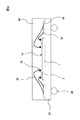
FIG. 7 is a process block flow diagram for explaining a main part of the manufacturing process such as probe inspection by the method of manufacturing a semiconductor integrated circuit device according to the embodiment of the present application. FIG. 9 is a schematic cross-sectional view of an example of the final form of the semiconductor integrated circuit device according to the manufacturing method of the semiconductor integrated circuit device of one embodiment of the present application. FIG. 10 is a schematic top view of a probe test state for explaining a state of probe inspection in the method of manufacturing a semiconductor integrated circuit device according to the embodiment of the present application. FIG. 11 is an enlarged view of a portion indicated by a broken line P in FIG. FIG. 12 is a schematic front view of a probe test state and the like for explaining a state of probe inspection and probe mark inspection in the method of manufacturing a semiconductor integrated circuit device according to the embodiment of the present application. Based on these drawings, a description will be given of the main part of the manufacturing process such as probe inspection by the method of manufacturing a semiconductor integrated circuit device according to the embodiment of the present application.
先ず、図7に示すように、ウエハ工程71が完了したウエハ11に対して、プローバ51(図12)によって、ウエハ・テスト131を実行する。図10及び図12に示すように、プローバ51は、ウエハ・プローブ部59とウエハ・アライメント部57(内部針跡検査部または内部プローブ痕検査部を兼ねる)に分かれている。ウエハ・テスト131(図7)におけるプローブ検査の実行工程107(図1)は、プローブ・カード50の開口部49を被検査チップ領域1に対向させた状態で、その周辺に設けられた実プローブ針47およびダミー・プローブ針48の先端をそれぞれ対応する実ボンディング・パッド3およびダミー・パッド5にコンタクトさせた状態で、電気的テストを実行するものである。プローブ検査の実行工程107(図1)においては、ウエハ11はウエハ・ステージ60上において、真空吸着されている。図10の点円Pの部分を拡大したのが、図11である。
First, as shown in FIG. 7, a
図7および図12に示すように、プローブ検査107を実行した後、ウエハ・ステージ60はウエハ11を乗せたまま、プローブ痕検査部57に移動して、そこで、光学観測系63により、内部プローブ痕検査111を実行する。プローブ痕検査111は、たとえば、ほぼ正方形のダミー・パッド5上のプローブ痕がダミー・パッド5の中心からどの方向にどれだけずれているかを観測することによって実行される。
As shown in FIGS. 7 and 12, after executing the
ここで、コンタクト位置のずれが許容範囲であれば、当該ウエハは次工程に送り、計測されたずれは、次の被検査ウエハの位置あわせにフィードバックされる。コンタクト位置のずれが一定以上である等、プローブ・テスト107の正常性を疑わせるようなデータがある場合には、再度、プローブ・テスト107を実行するか、当該ウエハは不良と判定する。なお、必要に応じて、プローブ痕検査111をスキップしてもよい。すなわち、全ウエハのほぼ全ての製品チップ領域(又は一部の製品チップ領域)および(もしあれば、以下同じ)検査用チップ領域に対して、実行してもよいし、ロット中の一部のウエハのほぼ全部の製品チップ領域(又は一部の製品チップ領域)および検査用チップ領域に対して、または一部のウエハのほぼ全部の製品チップ領域(又は一部の製品チップ領域)および検査用チップ領域の少なくとも一方に対してプローブ痕検査111を実行するようにしてもよい。なお、プローブ痕検査111は、外部針跡検査装置61を用いて、外部針跡検査112(図1)として、実行してもよい。ただし、この場合は、内部針跡検査装部57を使用するよりも、一般に時間を要する。
Here, if the displacement of the contact position is within an allowable range, the wafer is sent to the next process, and the measured displacement is fed back to the alignment of the next wafer to be inspected. If there is data that doubts the normality of the
図7に示すように、プローバ51による最後のテストが完了したウエハ11には、バック・グラインディング処理73が施された後、個別チップ1に分割するためのダイシング処理74が実行される。その後、分割されたチップ1に対して、図9及び図7に示すように、多層配線基板33上に(リードフレーム上でもよい)、DAF(Die Attach Film)等の接着部材を介して、ダイ・ボンディング75が実行される。続いて、図9及び図7に示すように、リード32と実ボンディング・パッド3の間で、金ワイヤ31等により、キャピラリを用いたワイヤ・ボンディング76が実行される。これにより、実ボンディング・パッド3上にボンディング・ボール12が形成される。
As shown in FIG. 7, the
その後、図9及び図7に示すように、エポキシ系樹脂等の封止レジン34により、たとえば、トランスファ・モールドにより、レジン封止77が実行される(圧縮モールド法を使用してもよい)。更に、図9及び図7に示すように、バンプ35が取り付けられる。
Thereafter, as shown in FIGS. 9 and 7, a resin sealing 77 is performed by a sealing
なお、ウエハ出荷製品については、バック・グラインディング処理73が施された後、直接、出荷工程80に移される。
The wafer shipment product is directly transferred to the
3.本願の一実施の形態の半導体集積回路装置の製造方法におけるウエハ・テスト工程の詳細説明(主に図1から図5、図8、及び図13から図16)
以下はカンチ・レバー型プローブ・カードを例にとり説明するが、セクション4に説明するアドバンスト・プローブ・カード等によるプローブ・テスト等にも、ほぼそのまま適用できる。また、以下の例では、摂氏100度以上、200度以下程度のテスト温度(第1の温度)で行われる高温ロジック・テスト131c(図1または図4)について具体的に説明するが、マイナス摂氏70度以上、零度以下程度のテスト温度(第1の温度)で行われる低温ロジック・テスト131d(図1または図4)、摂氏100度以上、200度以下程度のテスト温度(第1の温度)で行われる高温メモリ・テスト131b(図1または図4)、およびマイナス摂氏70度以上、零度以下程度のテスト温度(第1の温度)で行われる低温メモリ・テスト(一般に、非常温ウエハ・プローブ・テスト)にも、ほぼそのまま適用できる。なお、以下では、フラッシュ・メモリ部(一般にメモリ部)およびロジック部(ロジック・テストは、主にこの部分をテストする。たとえばファンクション・テスト等)を搭載した半導体集積回路装置(フラッシュ・メモリ混在チップ)のテスト(たとえばデータ・リテンション・テスト)を例にとり説明するが、フラッシュ・メモリ部を有さない半導体集積回路装置にも、適用できることは言うまでもない。
3. Detailed description of the wafer test process in the method of manufacturing a semiconductor integrated circuit device according to an embodiment of the present application (mainly FIGS. 1 to 5, FIG. 8, and FIGS. 13 to 16)
In the following, a cantilever type probe card will be described as an example, but the present invention can be applied almost as it is to a probe test using an advanced probe card or the like described in
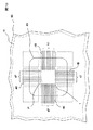
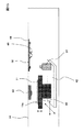
図1は本願の一実施の形態の半導体集積回路装置の製造方法における個々のプローバによるウエハ・テストの流れを示すプロセス・ブロック・フロー図である。図2は本願の一実施の形態の半導体集積回路装置の製造方法における個々のプローバ内でのウエハ・ステージの位置制御方法を説明するフロー・チャートである。図3は本願の一実施の形態の半導体集積回路装置の製造方法における個々のプローバ内でのウエハ・バッチに対する処理の流れを示すプロセス・ブロック・フロー図である。図4は本願の一実施の形態の半導体集積回路装置の製造方法におけるウエハ・テスト工程全体の流れを例示するプロセス・ブロック・フロー図である。図5は本願の一実施の形態の半導体集積回路装置の製造方法におけるウエハ・テスト工程に使用するプローバの一例を示すプローバ上面図である。図8は本願の一実施の形態の半導体集積回路装置の製造方法における個々のプローバ内でのウエハ・ステージの位置制御方法を説明するプローバ制御系の構成の一例を示すブロック図である。図13は本願の一実施の形態の半導体集積回路装置の製造方法における個々のプローバ内でのプローブ・カードとウエハの関係をカンチ・レバー型プローブ・カードを例にとり説明するための装置部分模式正面図(プローブ・カード部分)である。図14は本願の一実施の形態の半導体集積回路装置の製造方法における個々のプローバ内でのプローブ・カードとウエハの関係をカンチ・レバー型プローブ・カードを例にとり説明するための装置要部模式正面プロセス・フロー図(プローブ待機時)である。図15は本願の一実施の形態の半導体集積回路装置の製造方法における個々のプローバ内でのプローブ・カードとウエハの関係をカンチ・レバー型プローブ・カードを例にとり説明するための装置要部模式正面プロセス・フロー図(ウエハ・アライメント時またはプローブ痕検査時)である。図16は本願の一実施の形態の半導体集積回路装置の製造方法における個々のプローバ内でのプローブ・カードとウエハの関係をカンチ・レバー型プローブ・カードを例にとり説明するための装置要部模式正面プロセス・フロー図(針位置合わせ時)である。これらに基づいて、本願の一実施の形態の半導体集積回路装置の製造方法におけるウエハ・テスト工程の詳細を説明する。 FIG. 1 is a process block flow diagram showing the flow of wafer testing by individual probers in the method of manufacturing a semiconductor integrated circuit device according to one embodiment of the present application. FIG. 2 is a flowchart for explaining a wafer stage position control method in each prober in the method of manufacturing a semiconductor integrated circuit device according to the embodiment of the present application. FIG. 3 is a process block flow diagram showing a flow of processing for wafer batches within individual probers in the method of manufacturing a semiconductor integrated circuit device according to one embodiment of the present application. FIG. 4 is a process block flow diagram illustrating the flow of the entire wafer test process in the method of manufacturing a semiconductor integrated circuit device according to the embodiment of the present application. FIG. 5 is a prober top view showing an example of a prober used in the wafer test process in the method of manufacturing a semiconductor integrated circuit device according to the embodiment of the present application. FIG. 8 is a block diagram showing an example of a configuration of a prober control system for explaining a wafer stage position control method in each prober in the method of manufacturing a semiconductor integrated circuit device according to one embodiment of the present application. FIG. 13 is an apparatus partial schematic front view for explaining the relationship between a probe card and a wafer in each prober in the method of manufacturing a semiconductor integrated circuit device according to an embodiment of the present invention, taking a cantilever type probe card as an example. It is a figure (probe card part). FIG. 14 is a schematic diagram of an essential part of an apparatus for explaining the relationship between a probe card and a wafer in each prober in the method of manufacturing a semiconductor integrated circuit device according to an embodiment of the present invention, taking a cantilever probe card as an example. It is a front process flow figure (at the time of probe standby). FIG. 15 is a schematic diagram of an essential part of an apparatus for explaining the relationship between a probe card and a wafer in each prober in the method of manufacturing a semiconductor integrated circuit device according to an embodiment of the present invention, taking a cantilever probe card as an example. It is a front process flowchart (at the time of wafer alignment or a probe trace inspection). FIG. 16 is a schematic diagram of the main part of the apparatus for explaining the relationship between the probe card and the wafer in each prober in the method of manufacturing a semiconductor integrated circuit device according to the embodiment of the present invention, taking a cantilever probe card as an example. It is a front process flow figure (at the time of needle position alignment). Based on these, the details of the wafer test process in the manufacturing method of the semiconductor integrated circuit device according to the embodiment of the present application will be described.
まず、ウエハ・テスト工程の全体の流れを説明する。図4に示すように、フラッシュ・メモリ混在チップに関するウエハ・テスト工程131は、通常、測定温度(たとえば摂氏25度の常温、摂氏160度の高温、摂氏零下40度の低温)とテスト目的(データ・リテンション・テストその他のメモリ・テスト、ロジック・テスト等)が相違する複数のプローブ・テスト工程(第1のメモリ・テスト131a,第2のメモリ・テスト131b,第1のロジック・テスト131c,第2のロジック・テスト131d)とその間のたとえば摂氏250度程度の温度で行われるデータ・リテンション・ベーク等の高温ベーク工程(第1のベーク処理141、第2のベーク処理142)等から構成されている。量産プロセスでは、温度変更頻度が高いと、プローバの実質稼働時間が低下するので、通常、温度とテスト目的(メモリ・テストかロジック・テストか)の組み合わせの分だけ複数のプローバ51a,51b、51c,51dを準備して、個々のプローバ51a,51b、51c,51dは、できるだけ温度一定にしてウエハ・テスト131を実行する。もちろん、プローバの実質稼働時間が低下してもよい場合は、同一のプローバを温度の異なるウエハ・テストに使用してもよい。
First, the overall flow of the wafer test process will be described. As shown in FIG. 4, the
次に、図1および図5に基づいて、1枚のウエハについて、個々のプローバによるウエハ・テスト(非常温ウエハ・プローブ・テストの一例として高温ロジック・テスト131c)の流れを説明する。図1に示すように、たとえば、プローバ51(ここではロジック・テスト)のロード・ポート53に300φのウエハ(450φ、200φその他の径のウエハでもよい)をたとえば25枚(単位ロット)収容したフープ52(ウエハ搬送容器)を設置する(図1の搬送容器ロード・ステップ101)。次に、フープ52から検査対象である1枚のウエハ11をウエハ・ロボット54により、プローバ51の内部のプリ・アライメント部55に移送する(図1のウエハ搬入ステップ102)。次に、プリ・アライメント部55において、プリ・アライメント光学系62により、ウエハ11の周上の位置認識指標(ノッチ、オリエンテーション・フラットなど)を認識して、ウエハ11の配向を確認する(図1のプリ・アライメント・ステップ103)。このプリ・アライメントに要する時間は通常、30秒程度である。
Next, based on FIG. 1 and FIG. 5, the flow of a wafer test (a high
次に、プリ・アライメント103の結果に基づいて、ウエハ11を所定の配向で、テスト温度に設定されたウエハ・ステージ60上に、ウエハ11のデバイス面11aを上にして、セットする(図1のステージ上への移送ステップ104)。次に、ウエハ・ステージ60はウエハ11を載せたまま、XYテーブル42の移動に従って、ウエハ・アライメント部57に移動して、そこで、ウエハ・アライメント光学系63により、ウエハ・アライメント105(図1)が実行される(所要時間は一般に45秒程度である)。このウエハ・アライメント105の際には、図15に示すように、ウエハ・アライメント光学系63がウエハ・ステージ60の直上に来るように、XYテーブル42が水平方向に移動する。その状態で、必要に応じて、XYテーブル42が水平移動し、ウエハ・ステージ60が鉛直方向に移動して、ウエハ11のデバイス面11aを光学的に観測して登録されている基準図形を抽出して、ウエハ上の基準点を認識する。図15からわかるように、ウエハ・アライメント光学系63はプローバ51の本体に固定されている。同様に、プローブ・カード50もカード・ホルダ44を介して、プローバ51の本体に固定されている。一方、針位置合わせ光学系64およびウエハ・ステージ60はXYテーブル42上に固定されている。
Next, based on the result of the pre-alignment 103, the
次に、XYテーブル42がシフトして、針位置合わせ光学系64がプローブ・カード50の下部へ移動して、そこで、針位置合わせ106(図1)が実行される(所要時間は一般に1分程度である)。これで、プローバ51は、ウエハ11上の回路パターンの位置とプローブ・カード50上のプローブ針先端部の位置を認識したことになる。針位置合わせ106の際には、図16に示すように、針位置合わせ光学系64がプローブ・カード50のプローブ針46の直下に来るように、XYテーブル42が水平方向に移動する。その状態で、必要に応じて、XYテーブル42が水平移動し、ウエハ・ステージ60が鉛直方向に移動して、基準となるプローブ針46の針先を光学的に観測して、プローブ針46の基準点(プローブ・カード50側の基準点)を認識する。
Next, the XY table 42 shifts and the needle alignment
次に、ウエハ・ステージ60はウエハ11を載せたまま、XYテーブル42の移動に従って、プローブ部59に移動する。この状態で、プローブ・カード50の温度とテスト温度の際が大きい場合は、待機する。プローブ・カード50の温度とテスト温度の際が小さい場合は、プローブ針をウエハ11上のボンディング・パッドにコンタクトさせた状態で電気的試験を実行する(図1の電気的試験実行ステップ107)。電気的試験の実行の際には、図14に示すように、ウエハ・ステージ60がプローブ・カード50の直下に来るように、XYテーブル42が水平方向に移動する。そして、XYテーブル42が、通常の移動時よりもプローブ・カード50に接近する。その状態で、所望の水平相互位置に来ると、プローブ針46とウエハ11上のボンディング・パッドとのコンタクトが行われ、電気的試験が実行される。一箇所の測定が完了すると、リリース、近接移動、およびコンタクト動作(単一のコンタクトでウエハ全体をテストすることもある。いわゆるフル・ウエハ・テストである)を繰り返して、ウエハ11の全体に対して電気的テストを実行する。
Next, the
プローブ針による電気的試験107が完了すると、ウエハ・ステージ60はウエハ11を載せたまま、XYテーブル42の移動に従って、ウエハ・ロード&アンロード部56へ移動する。そこで、ウエハ・ロボット54がウエハ11をウエハ・ステージ60上からピック・アップして(図1のウエハ・リリース・ステップ108)、装置外に搬出する(図1のウエハ搬出ステップ109)。全てのウエハの電気的試験が完了すると、フープ52がロード・ポート53からアンロードされる(図1のウエハ搬送容器アンロード・ステップ110)。
When the
ここで、電気的試験実行ステップ107の後、必要に応じて、ウエハ針跡検査を実行する。ウエハ針跡検査は、ウエハ・アライメント部57における内部ウエハ針跡検査111としてもよいし、外部針跡検査装置61による外部ウエハ針跡検査112としてもよい。一般に、内部ウエハ針跡検査111の方が効率がよいと考えられる。内部ウエハ針跡検査111は図15に示す状態で、実行される。
Here, after the electrical
次に、図3に基づいて、一つのロット全体(たとえば25枚のウエハ11を収容したフープ52)についての個々のプローバによる非常温ウエハ・テスト131c(131b,131d)の流れを説明する。図3に示すように、まず、ロットの最初のウエハ11に対してプローブ検査121(電気的試験)を実行する前に、通常、ウエハ11をテスト温度に温度設定されたウエハ・ステージ60に載せたまま、ウエハ11の上面11aをプローブ・カード50の直下で近接させて待機させることにより、プローブ・カード50の温度をテスト温度に近い温度に安定させるための近接待機処理125(第1の安定化待機)すなわちプリ・ヒートを実行する(所要時間通常5分程度)。なお、プローブ・カード50の温度がすでに所定の検査温度で安定しているときは、この第1の安定化待機ステップをスキップすることができることは言うまでもない。
Next, based on FIG. 3, the flow of the emergency
プローブ・カード50の温度が安定すると、ロットの最初のウエハ11に対してプローブ検査121(電気的試験)を実行する(第1のウエハに対するプローブ検査の実行)。続いて、たとえば、前記最初のウエハ11に対して、針跡検査122を実行する。針跡検査122は、たとえば、内部針跡検査として実行する。この針跡検査122の標準的処理時間(15分から30分)と比較して、長時間を要した場合などには、プローブ・カード50の温度がテスト温度と相当相違している場合があるので、プローブ・カード50の温度をテスト温度に近い温度に安定させるための近接待機処理126(第2の安定化待機)を実行する。一方、針跡検査122の標準的処理時間と比較して、長時間を要しない場合などには、この第2の安定化待機126をスキップすることができる。次に、ロットの2番目のウエハ11に対してプローブ検査123(電気的試験)を実行する(第2のウエハに対するプローブ検査の実行)。このプローブ検査121、123の所要時間は、ウエハ1枚あたり、標準的には2から7時間程度である。
When the temperature of the
以後は、通常、針跡検査122および安定化待機125、126等を実施することなく、順次、ロットを構成する全ての検査対象ウエハに対して、プローブ検査(電気的試験)を実行し、最終的にロットの最後のウエハ11に対して、電気的試験124を実行する。なお、必要があれば、針跡検査122(後の針跡検査)および安定化待機125、126(後の安定化待機)等を毎回または適宜、選択的に実行してもよい。
Thereafter, probe inspection (electrical test) is performed on all inspection target wafers that make up a lot in sequence without performing
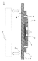
次に、図13に基づいて、プローブ針46によるウエハ11に対する電気的試験(すなわちプローブ検査)または安定化待機125、126(後の安定化待機を含む)を実施する際のウエハ・ステージ60とプローブ・カード50の関係を説明する。図13に示すように、プローブ針先端からウエハ上面(正確にはボンディング・パッド上面)間の距離、すなわち、プローブ針・ウエハ間クリアランスD(プローブ針自体の高さは、種類によって異なるが、一般に3ミリ・メートルから15ミリ・メートル程度である)は、処理の内容によって以下のように設定するのが好適である。プローブ検査の実行中でプローブ針がボンディング・パッドにコンタクトしているときは、もちろんプローブ針・ウエハ間クリアランスDはゼロとなる。同一のウエハ上で次の試験サイトに移動する際(ウエハ内移動時)等は、非接触近接状態で移動する。また、安定化待機125、126の際にも、このウエハ内移動時と同等な非接触近接状態に維持されることが、精度の確保または温度均一化の観点から好適である。これら以外の通常の移動時(ウエハ・ステージ60が移動するとき)、たとえば、プローブ部59からウエハ・ステージ60が外部(プローバ51内のプローブ部59以外の部分)に移動するとき、および、ウエハ・ステージ60が外部からプローブ部59へ移動するとき等は、非接触近接状態よりも大きな通常間隔を維持した状態で移動するのが、動作上の安定性または安全性の観点から好適である。なお、非接触近接状態におけるプローブ針・ウエハ間クリアランスDは、たとえば、200マイクロ・メートルから700マイクロ・メートル程度が好適である。また、通常間隔の際のプローブ針・ウエハ間クリアランスDは、たとえば、10ミリ・メートルから40ミリ・メートル程度が好適である。
Next, referring to FIG. 13, the
次に、図2に基づいて、プローブ・カード50の温度安定化システムについて説明する。ウエハ・ステージ60は通常、その内部の冷却系または加熱系によって検査温度に保持されているので、ウエハ・ステージ60がプローブ・カード50の直下にある状態、すなわち、プローブ検査107(図1)や安定化待機125、126(図3)の際には、プローブ・カード50は検査温度(第1の温度)に近い温度になっていると考えられる。しかし、個々のプローバ51(図1)によるウエハ・テスト131(図3)の全期間を見ると、多くの期間において、ウエハ・ステージ60がプローブ・カード50の直下にない場合(ウエハ・ステージ不在期間)がある。このウエハ・ステージ不在期間には、当然、プローブ・カード50の温度は常温に近づく方向で、検査温度から離れてゆく。ウエハ・ステージ不在期間の内、いろいろな原因で発生するが、最も問題となるのは、たとえば、針跡検査122(図3)で予想外に長時間を要する場合である。これは、針跡検査122がマニュアル操作を要求する場合が多いからである。人的要素が介在するマニュアル作業では、人の不在、マニュアル操作要求の多重発生、錯誤等により長時間放置されることが多い。これらの結果、ウエハ・ステージ不在期間が無駄に長時間化する事態が発生する。長時間放置することによって、プローブ・カード50の温度が、検査温度から著しくずれると、次にプローブ・カード50の温度が安定して、時検査温度の近傍になるまで、2時間以上かかる場合もある。
Next, a temperature stabilization system for the
この問題を回避するには、以下のような処理が有用である。すなわち、ウエハ・ステージ不在期間においては、自動的にプローバ51の動作を監視することによって、ウエハ・ステージ60がプローブ・カード50の下方にない連続した時間であってウエハ・プローバ51が実質的に有効な動作をしていない遊休時間を監視し、この遊休時間が第1の時間間隔以上になった場合は、ウエハ11がセットされ、第1の温度(検査温度)に保持されたウエハ・ステージ60をプローブ・カード50の下方に自動的に移動させ、そこで待機させる(近接待機することが望ましい)。この手順を図2および図8に基づいて、説明する。図2および図8に示すように、プローバ51内に(外部でもよい)設けられたプローバ動作監視系65は、プローバ制御系66を監視することによって、XYテーブル制御系67、ウエハ位置合わせ制御系68、針位置合わせ制御系69等の動作を監視する。そして、プローバ動作監視系65は、まず、ウエハ・ステージ60がプローブ・カード50の直下にある状態(ウエハ・ステージ滞在期間)か、ウエハ・ステージ60がプローブ・カード50の直下にない状態(ウエハ・ステージ不在期間)か否かを判断する(ウエハ・ステージ位置判定151)。ここで、ウエハ・ステージ60がプローブ・カード50の直下にある状態であれば、プローバ動作監視系65は、そのままの状態を維持する。しかし、ウエハ・ステージ60がプローブ・カード50の直下にない状態であれば、プローバ動作監視系65は、ウエハ・ステージ60に関係するプローバ51の動作を監視し(ウエハ・ステージ関連動作監視152)、不必要な連続的なウエハ・ステージ不在期間の長さをカウントする。そして、この遊休時間が所定の時間間隔(第1の時間間隔、たとえば5分程度である。一般に2分以上、20分未満が好適である。更に3分以上、18分未満が好適である)以上になったか否かを判定する(遊休時間長さ判定153)。ここで、遊休時間が所定の時間間隔未満であれば、プローバ動作監視系65は、そのままの状態を維持する。しかし、遊休時間が所定の時間間隔以上であれば、プローバ動作監視系65は、プローバ制御系66にウエハ・ステージ60をプローブ・カード50の直下に復帰させるように指示を出し、ウエハ・ステージ60をプローブ・カード50の直下に復帰させ(プローブ・カード直下復帰154)、安定化待機状態(近接待機することが望ましい)とする。この安定化待機状態では、非接触近接状態と同等なプローブ針・ウエハ間クリアランスDとすることが、短時間の温度安定の観点から好適である。しかし、この安定化時間が若干伸びてもよい場合には、プローブ針・ウエハ間クリアランスDを通常間隔またはそれと非接触近接状態と同等なプローブ針・ウエハ間クリアランスDの間の適切な値としてもよい。
In order to avoid this problem, the following processing is useful. In other words, during the absence of the wafer stage, the operation of the
4.本願の一実施の形態の半導体集積回路装置の製造方法におけるウエハ・テスト工程に使用する他のプローブ・カードの説明(主に図17及び図18)
近年、パッド・ピッチの狭小化への対応、または同時テスト・チップ個数の増加(一回のコンタクトで全てのチップをテストするフル・ウエハ・テストまたは数回のコンタクトで全てのチップをテストするセミ・フル・ウエハ・テスト)のために、従来のカンチ・レバー型プローブ・カードに代わって、いろいろな種類の、いわゆるアドバンスト・プローブ・カードが使用され始めている。これらの各種のアドバンスト・プローブ・カードは、セクション3の例においてカンチ・レバー型プローブ・カードに代えて、適用できる。以下では簡単に、その構造を説明する。
4). Description of other probe cards used in the wafer test process in the method of manufacturing a semiconductor integrated circuit device according to the embodiment of the present application (mainly FIGS. 17 and 18)
In recent years, it has been possible to reduce the pad pitch or increase the number of simultaneous test chips (full wafer test that tests all chips with one contact or semi-test that tests all chips with several contacts) For the full wafer test), various types of so-called advanced probe cards have begun to be used in place of conventional cantilever probe cards. These various advanced probe cards can be applied in place of the cantilever type probe card in the example of
図17は本願の一実施の形態の半導体集積回路装置の製造方法におけるウエハ・テスト工程に使用する他のプローブ・カード、すなわち、垂直針系プローブ・カード(アドバンスト・プローブ・カードの一種)の一例を示す断面図(セクション3の図13にほぼ対応、以下おなじ)である。図18は本願の一実施の形態の半導体集積回路装置の製造方法におけるウエハ・テスト工程に使用する他のプローブ・カード、すなわち、マイクロ・カンチ・レバー型プローブ・カード(アドバンスト・プローブ・カードの一種)の一例を示す断面図である。これらに基づいて、本願の一実施の形態の半導体集積回路装置の製造方法におけるウエハ・テスト工程に使用する他のプローブ・カードの構造の概要を説明する。
FIG. 17 is an example of another probe card used in the wafer test process in the method of manufacturing a semiconductor integrated circuit device according to the embodiment of the present application, that is, an example of a vertical needle probe card (a kind of advanced probe card). FIG. 14 is a cross-sectional view (substantially corresponding to FIG. 13 of
先ず、垂直針系プローブ・カードを説明する。図17に示すように、プローブ・カードの本体50は、通常のプローブ・カードと同様に、印刷配線基板(一般に、テスト品種ごとに代わる)で構成されている。プローブ・カードの本体50の上面には、通常のプローブ・カードと同様に、リング状に配列されたコネクタ部43(またはポゴピン・コンタクト部)が設けられており、そこで、テスト・ヘッド45を介して、テスタ(セクション3のロジック・テストの場合はロジック・テスタ)と接続されている。一方、プローブ・カードの本体50の下面には、リング状金属枠体41および固定ネジ38を介して、多数のプローブ針46(たとえば、パラジュウム合金製)を保持したセラミック製の針ホールダ37が固定されている。セラミック製の針ホールダ37内には、針サポート空洞39があり、その天井部分でプローブ針46は固定されており、プローブ針46の各下端部は、針サポート空洞39の床部の細孔を貫通して、比較的自由に保持されている。これらの多数のプローブ針46は、インターポーザ40を介して、プローブ・カードの本体50と接続されている。
First, the vertical needle probe card will be described. As shown in FIG. 17, the
次に、マイクロ・カンチ・レバー型プローブ・カードを説明する。図18に示すように、プローブ・カードの本体50は、通常のプローブ・カードと同様に、印刷配線基板(一般に、テスト品種ごとに代わる)で構成されている。プローブ・カードの本体50の上面には、図17の例と同様に、リング状に配列されたコネクタ部43(またはポゴピン・コンタクト部)が設けられており、そこで、テスト・ヘッド45を介して、テスタ(セクション3のロジック・テストの場合はロジック・テスタ)と接続されている。一方、プローブ・カードの本体50の下面には、リング状金属枠体41を介して、多数のプローブ針46(たとえば薄膜金属板をリソグラフィによりパターニングしたもの)を保持したセラミック製の針ホールダ37が固定されている。これらの多数のプローブ針46は、インターポーザ40を介して、プローブ・カードの本体50と接続されている。この場合、先の垂直針系プローブ・カードと比較して、プローブ針46の上下自由度が小さいので、プローブ・カードの本体50の上面には、たわみ防止用の(たとえばステンレス製の)スティフナ(補強構造体)36が固定されている。
Next, a micro cantilever type probe card will be described. As shown in FIG. 18, the
5.サマリ
以上本発明者によってなされた発明を実施形態に基づいて具体的に説明したが、本発明はそれに限定されるものではなく、その要旨を逸脱しない範囲において種々変更可能であることは言うまでもない。
5. Summary The invention made by the present inventor has been specifically described based on the embodiments. However, the present invention is not limited thereto, and it goes without saying that various changes can be made without departing from the scope of the invention.
例えば、前記実施の形態では、プローバの形式として、主に従来型のカンチ・レバー型プローブ・カードについて、具体的に説明したが、本願はそれに限定されるものではなく、バーチカル型プローブ・カード、スプリング・ピン型プローブ・カード、薄膜プローブ等のフォトリソグラフィやMEMS技術を活用したアドバンスト・プローブ・カードまたはMEMSタイプのプローブ・カード等によるプローブ検査にも適用できることは言うまでもない。 For example, in the above-described embodiment, the conventional cantilever type probe card has been specifically described as a prober type. However, the present application is not limited thereto, and a vertical type probe card, Needless to say, the present invention can also be applied to probe inspection using an advanced probe card or a MEMS type probe card utilizing a photolithography or MEMS technology such as a spring pin type probe card or a thin film probe.
また、前記実施の形態では、2列にボンディング・パッドを配置したチップ・レイアウトを例にとり具体的に説明したが、本願はそれに限定されるものではなく、1列にボンディング・パッドを配置したチップ・レイアウトにも3列以上およびマトリクス状にボンディング・パッドを配置したチップ・レイアウトにも適用できることは言うまでもない。 In the above-described embodiment, the chip layout in which the bonding pads are arranged in two rows has been specifically described as an example. However, the present application is not limited thereto, and the chip in which the bonding pads are arranged in one row. Needless to say, the present invention can also be applied to a chip layout in which bonding pads are arranged in three or more columns and in a matrix.
1 チップまたはウエハ上のチップ領域(被検査チップ領域)
1a チップの上面(またはデバイス面)
3 実ボンディング・パッド
5 ダミー・パッド(針跡検査用パッド)
7 内部回路領域
11 ウエハ
11a ウエハの上面(またはデバイス面)
12 ボール
31 ボンディング・ワイヤ
32 リード
33 配線基板
34 レジン封止部
35 バンプ電極
36 スティフナ(補強構造体)
37 (セラミック製の)針ホールダ
38 固定ネジ
39 針サポート空洞
40 インターポーザ
41 リング状金属枠体
42 XYテーブル
43 ポゴピン(またはコネクタ部)
44 カード・ホルダ
45 テスト・ヘッド
46 プローブ針
47 実プローブ針
48 ダミー・プローブ針
49 プローブ・カードの開口
50 プローブ・カード(またはプローブ・カード本体の配線基板)
51、51a,51b,51c,51d プローバ
52 ウエハ搬送容器(フープ)
53 ウエハ搬送容器用ポート
54 ウエハ搬送ロボット
55 プリ・アライメント部
56 ウエハ・ロード&アンロード部
57 ウエハ・アライメント部(内部針跡検査部)
59 プローブ部
60 ウエハ・ステージ
61 外部針跡検査装置
62 プリ・アライメント光学系
63 ウエハ・アライメント光学系
64 針位置合わせ光学系
65 プローバ制御監視系
66 プローバ制御系
67 XYテーブル制御系
68 ウエハ位置合わせ制御系
69 針位置合わせ制御系
71 (ウエハ・テストに先行する)ウエハ工程
73 バック・グラインディング処理
74 ウエハ・ダイシング
75 ダイ・ボンディング
76 ワイヤ・ボンディング
77 レジン封止
78 バンプ取り付け
79 最終テスト
80 出荷
101 ウエハ搬送容器ロード
102 ウエハ搬入
103 プリ・アライメント
104 ウエハがステージ上に移動
105 ウエハ・アライメント
106 針位置合わせ
107 プローブ実行(電気的試験実行)
108 ウエハがステージ上から移動
109 ウエハ搬出
110 ウエハ搬送容器アンロード
111 内部針跡検査
112 外部針跡検査
121 第1のウエハに対してプローブ実行
122 第1のウエハに対して針跡検査
123 第2のウエハに対してプローブ実行
124 ロットの最後のウエハに対してプローブ実行
125 第1の安定化待機
126 第2の安定化待機
130 ウエハ・テスト以前のウエハ・プロセス
131 ウエハ・テスト
131a 第1のメモリ・テスト
131b 第2のメモリ・テスト
131c 第1のロジック・テスト
131d 第2のロジック・テスト
132 BG(バック・グラインディング)
133 ダイシング(ウエハのチップへの分割)
134 組み立て(ダイ・ボンディング、ワイヤ・ボンディング、封止等)
135 最終電気テスト
136 出荷
141 第1のベーク処理
142 第2のベーク処理
151 ウエハ・ステージがプローブ・カードの直下領域にあるかを監視
152 ウエハ・ステージに関連するプローバの動作を監視
153 不必要にプローブ・カードの直下領域外にあった時間が連続して第1の時間を超えたかを判断
154 ウエハ・ステージをプローブ・カードの直下領域に復帰
D プローブ針先端からウエハ上面(正確にはボンディング・パッド上面)間の距離
P 点線の円で表示した部分
1 Chip area on chip or wafer (inspected chip area)
1a Top surface of chip (or device surface)
3
7
12
37 Needle holder (made of ceramic) 38
44
51, 51a, 51b, 51c,
53 Wafer
59
108 Wafer moves from
133 Dicing (Division of wafer into chips)
134 Assembly (die bonding, wire bonding, sealing, etc.)
135 Final Electrical Test 136
D Distance between probe needle tip and wafer upper surface (more precisely, bonding pad upper surface) P Portion indicated by dotted circle
Claims (20)
(a)ウエハ・プローバ内において、常温と異なる第1の温度に保持されたウエハ・ステージ上に、ウエハをセットする工程;
(b)前記工程(a)の後、前記ウエハ・プローバ内において、前記ウエハがセットされ、前記第1の温度に保持された前記ウエハ・ステージをプローブ・カードの下方に移動させる工程;
(c)前記工程(b)の後、前記ウエハ・プローバ内において、前記ウエハがセットされ、前記第1の温度に保持された前記ウエハ・ステージが、前記プローブ・カードの下方にある状態で、前記プローブ・カードを用いて、前記第1の温度における前記被検査ウエハに対する電気的試験を実行する工程;
(d)前記工程(c)の後、前記ウエハ・プローバ内において、前記ウエハがセットされ、前記第1の温度に保持された前記ウエハ・ステージを前記プローブ・カードの下方外に移動させる工程;
(e)前記工程(d)の後、前記ウエハ・プローバ内において、前記第1の温度に保持された前記ウエハ・ステージ上の前記ウエハを、前記ウエハ・ステージの外部へ移動させる工程、
ここで、前記ウエハ・プローバの動作中において、前記ウエハ・ステージが前記プローブ・カードの下方にない連続した時間であって前記ウエハ・プローバが実質的に有効な動作をしていない遊休時間を監視し、この遊休時間が第1の時間間隔以上になった場合は、前記ウエハがセットされ、前記第1の温度に保持された前記ウエハ・ステージを前記プローブ・カードの下方に自動的に移動させる。 A method of manufacturing a semiconductor integrated circuit device including the following steps:
(A) setting a wafer on a wafer stage held at a first temperature different from room temperature in a wafer prober;
(B) After the step (a), in the wafer prober, moving the wafer stage in which the wafer is set and held at the first temperature below the probe card;
(C) After the step (b), in the wafer prober, the wafer stage set and held at the first temperature is below the probe card, Performing an electrical test on the wafer to be inspected at the first temperature using the probe card;
(D) after the step (c), the step of moving the wafer stage, in which the wafer is set and held at the first temperature, to the outside of the probe card in the wafer prober;
(E) after the step (d), moving the wafer on the wafer stage held at the first temperature outside the wafer stage in the wafer prober;
Here, during the operation of the wafer prober, the idle time during which the wafer stage is not under the probe card and the wafer prober is not operating effectively is monitored. If the idle time exceeds the first time interval, the wafer is set, and the wafer stage held at the first temperature is automatically moved below the probe card. .
(a)ウエハ・プローバに複数のウエハを収容したウエハ搬送容器をロードする工程;
(b)前記工程(a)の後、前記ウエハ搬送容器内の前記複数のウエハの内の第1のウエハを、前記ウエハ・プローバ内に移送する工程;
(c)前記ウエハ・プローバ内において、常温と異なる第1の温度に保持されたウエハ・ステージ上に、第1のウエハをセットする工程;
(d)前記工程(c)の後、前記ウエハ・プローバ内において、前記第1のウエハがセットされ、前記第1の温度に保持された前記ウエハ・ステージをプローブ・カードの下方に移動させる工程;
(e)前記工程(d)の後、前記ウエハ・プローバ内において、前記第1のウエハがセットされ、前記第1の温度に保持された前記ウエハ・ステージが、前記プローブ・カードの下方にある状態で、前記プローブ・カードの温度が安定するまで待機する工程;
(f)前記工程(d)および(e)の内の後の工程の後、前記ウエハ・プローバ内において、前記第1のウエハがセットされ、前記第1の温度に保持された前記ウエハ・ステージが、前記プローブ・カードの下方にある状態で、前記プローブ・カードを用いて、前記第1の温度における前記第1のウエハに対する電気的試験を実行する工程;
(g)前記工程(f)の後、前記ウエハ・プローバ内において、前記第1のウエハがセットされ、前記第1の温度に保持された前記ウエハ・ステージを前記プローブ・カードの下方外に移動させる工程;
(h)前記工程(g)の後、前記第1のウエハがセットされ、前記第1の温度に保持された前記ウエハ・ステージが前記プローブ・カードの下方外に移動した状態で、前記第1のウエハに対して、針跡検査を実行する工程;
(i)前記工程(g)および(h)の内の後の工程の後、前記ウエハ・プローバ内において、前記第1の温度に保持された前記ウエハ・ステージ上の前記第1のウエハを、前記ウエハ・ステージの外部へ移動させる工程;
(j)前記工程(i)の後、前記第1のウエハを前記ウエハ搬送容器内に移送する工程;
(k)前記工程(i)の後、前記ウエハ搬送容器内の前記複数のウエハの内の前記第1のウエハ以外の各ウエハに対して、順次、工程(b)から(d)、工程(f)から(g)、および工程(i)から(j)を繰り返す工程、
ここで、前記ウエハ・プローバの動作中において、前記ウエハ・ステージが前記プローブ・カードの下方にない連続した時間であって前記ウエハ・プローバが実質的に有効な動作をしていない遊休時間を監視し、この遊休時間が第1の時間間隔以上になった場合は、前記第1のウエハがセットされ、前記第1の温度に保持された前記ウエハ・ステージを前記プローブ・カードの下方に自動的に移動させる。 A method of manufacturing a semiconductor integrated circuit device including the following steps:
(A) loading a wafer transfer container containing a plurality of wafers into a wafer prober;
(B) after the step (a), transferring a first wafer of the plurality of wafers in the wafer transfer container into the wafer prober;
(C) setting the first wafer on a wafer stage held at a first temperature different from normal temperature in the wafer prober;
(D) After the step (c), the step in which the first wafer is set in the wafer prober and the wafer stage held at the first temperature is moved below the probe card. ;
(E) After the step (d), the wafer stage in which the first wafer is set and maintained at the first temperature is below the probe card in the wafer prober. Waiting for the temperature of the probe card to stabilize;
(F) After the subsequent steps of steps (d) and (e), the wafer stage in which the first wafer is set and held at the first temperature in the wafer prober. Performing an electrical test on the first wafer at the first temperature using the probe card with the probe card underneath the probe card;
(G) After the step (f), in the wafer prober, the first wafer is set, and the wafer stage held at the first temperature is moved out of the probe card. The step of causing;
(H) After the step (g), in the state where the first wafer is set and the wafer stage held at the first temperature is moved to the lower outside of the probe card, Performing a needle mark inspection on a wafer of
(I) after the later steps of the steps (g) and (h), the first wafer on the wafer stage held at the first temperature in the wafer prober; Moving the wafer stage to the outside;
(J) After the step (i), a step of transferring the first wafer into the wafer transfer container;
(K) After the step (i), the steps (b) to (d), step (b) are sequentially performed on each wafer other than the first wafer among the plurality of wafers in the wafer transfer container. repeating steps f) to (g) and steps (i) to (j);
Here, during the operation of the wafer prober, the idle time during which the wafer stage is not under the probe card and the wafer prober is not operating effectively is monitored. If the idle time exceeds the first time interval, the first wafer is set, and the wafer stage held at the first temperature is automatically moved below the probe card. Move to.
Priority Applications (1)
| Application Number | Priority Date | Filing Date | Title |
|---|---|---|---|
| JP2008224444A JP5317330B2 (en) | 2008-09-02 | 2008-09-02 | Manufacturing method of semiconductor integrated circuit device |
Applications Claiming Priority (1)
| Application Number | Priority Date | Filing Date | Title |
|---|---|---|---|
| JP2008224444A JP5317330B2 (en) | 2008-09-02 | 2008-09-02 | Manufacturing method of semiconductor integrated circuit device |
Publications (2)
| Publication Number | Publication Date |
|---|---|
| JP2010062237A true JP2010062237A (en) | 2010-03-18 |
| JP5317330B2 JP5317330B2 (en) | 2013-10-16 |
Family
ID=42188746
Family Applications (1)
| Application Number | Title | Priority Date | Filing Date |
|---|---|---|---|
| JP2008224444A Expired - Fee Related JP5317330B2 (en) | 2008-09-02 | 2008-09-02 | Manufacturing method of semiconductor integrated circuit device |
Country Status (1)
| Country | Link |
|---|---|
| JP (1) | JP5317330B2 (en) |
Cited By (1)
| Publication number | Priority date | Publication date | Assignee | Title |
|---|---|---|---|---|
| CN113823577A (en) * | 2020-06-19 | 2021-12-21 | 东京毅力科创株式会社 | Contact releasing method in inspection apparatus and inspection apparatus |
Citations (7)
| Publication number | Priority date | Publication date | Assignee | Title |
|---|---|---|---|---|
| JPH1116966A (en) * | 1997-06-19 | 1999-01-22 | Sanyo Electric Co Ltd | Pad arrangement method of one-chip microcomputer |
| JPH11121558A (en) * | 1997-10-20 | 1999-04-30 | Tokyo Electron Ltd | Probe method and probe device thereof |
| JP2000294606A (en) * | 1999-04-07 | 2000-10-20 | Nec Corp | Inspecting device for semiconductor wafer |
| JP2002057196A (en) * | 2000-08-07 | 2002-02-22 | Plum Five Co Ltd | Method and device for probe |
| JP2002525887A (en) * | 1998-09-30 | 2002-08-13 | クリーダンス システムズ コーポレイション | Insulation plate for probe card |
| JP2004266206A (en) * | 2003-03-04 | 2004-09-24 | Nec Yamagata Ltd | Prober device, preheating method of probe card and its program |
| JP2007212472A (en) * | 2007-03-28 | 2007-08-23 | Renesas Technology Corp | Manufacturing method of semiconductor integrated circuit, and probe card |
-
2008
- 2008-09-02 JP JP2008224444A patent/JP5317330B2/en not_active Expired - Fee Related
Patent Citations (7)
| Publication number | Priority date | Publication date | Assignee | Title |
|---|---|---|---|---|
| JPH1116966A (en) * | 1997-06-19 | 1999-01-22 | Sanyo Electric Co Ltd | Pad arrangement method of one-chip microcomputer |
| JPH11121558A (en) * | 1997-10-20 | 1999-04-30 | Tokyo Electron Ltd | Probe method and probe device thereof |
| JP2002525887A (en) * | 1998-09-30 | 2002-08-13 | クリーダンス システムズ コーポレイション | Insulation plate for probe card |
| JP2000294606A (en) * | 1999-04-07 | 2000-10-20 | Nec Corp | Inspecting device for semiconductor wafer |
| JP2002057196A (en) * | 2000-08-07 | 2002-02-22 | Plum Five Co Ltd | Method and device for probe |
| JP2004266206A (en) * | 2003-03-04 | 2004-09-24 | Nec Yamagata Ltd | Prober device, preheating method of probe card and its program |
| JP2007212472A (en) * | 2007-03-28 | 2007-08-23 | Renesas Technology Corp | Manufacturing method of semiconductor integrated circuit, and probe card |
Cited By (2)
| Publication number | Priority date | Publication date | Assignee | Title |
|---|---|---|---|---|
| CN113823577A (en) * | 2020-06-19 | 2021-12-21 | 东京毅力科创株式会社 | Contact releasing method in inspection apparatus and inspection apparatus |
| CN113823577B (en) * | 2020-06-19 | 2024-01-05 | 东京毅力科创株式会社 | Contact releasing method in inspection device and inspection device |
Also Published As
| Publication number | Publication date |
|---|---|
| JP5317330B2 (en) | 2013-10-16 |
Similar Documents
| Publication | Publication Date | Title |
|---|---|---|
| TWI442495B (en) | Check the device | |
| KR101105230B1 (en) | Bonding Head And Thermocompression Bonding Method Using The Same | |
| JPH0792479B2 (en) | Parallelism adjustment method for probe device | |
| JP2009198407A (en) | Needle mark transfer member of probe, and probe device | |
| US11035898B1 (en) | Device and method for thermal stabilization of probe elements using a heat conducting wafer | |
| JP2010276541A (en) | Thin-film probe sheet, method of manufacturing the same, probe card, and semiconductor chip inspecting apparatus | |
| JP2003344498A (en) | Semiconductor tester | |
| JP4932618B2 (en) | Inspection method and program recording medium recording this method | |
| JP5317330B2 (en) | Manufacturing method of semiconductor integrated circuit device | |
| JP2008103528A (en) | Inspection method and probe card for semiconductor device | |
| JP2006339456A (en) | Electronic device manufacturing method and probe card manufacturing method | |
| JP2010267689A (en) | Method of manufacturing semiconductor integrated circuit device | |
| JP2008300655A (en) | Testing apparatus for wafer, and testing method | |
| JP2004266206A (en) | Prober device, preheating method of probe card and its program | |
| US11835574B2 (en) | Semiconductor testing apparatus for wafer probing testing and final packaged IC testing | |
| WO2016084147A1 (en) | Wafer inspection method | |
| JP5317753B2 (en) | Bonder device | |
| US11573266B2 (en) | Electronic device temperature test on strip film frames | |
| JP5527794B2 (en) | Manufacturing method of semiconductor device | |
| JP2008053282A (en) | Prober | |
| JP2003344478A (en) | Inspection device and inspection method | |
| JP2002196017A (en) | Probing card | |
| Tuckerman et al. | A cost-effective wafer-level burn-in technology | |
| JP5323406B2 (en) | Manufacturing method of semiconductor integrated circuit device | |
| JP7277845B2 (en) | prober |
Legal Events
| Date | Code | Title | Description |
|---|---|---|---|
| A711 | Notification of change in applicant |
Free format text: JAPANESE INTERMEDIATE CODE: A712 Effective date: 20100527 |
|
| A621 | Written request for application examination |
Free format text: JAPANESE INTERMEDIATE CODE: A621 Effective date: 20110812 |
|
| A977 | Report on retrieval |
Free format text: JAPANESE INTERMEDIATE CODE: A971007 Effective date: 20130424 |
|
| A131 | Notification of reasons for refusal |
Free format text: JAPANESE INTERMEDIATE CODE: A131 Effective date: 20130502 |
|
| A521 | Written amendment |
Free format text: JAPANESE INTERMEDIATE CODE: A523 Effective date: 20130611 |
|
| TRDD | Decision of grant or rejection written | ||
| A01 | Written decision to grant a patent or to grant a registration (utility model) |
Free format text: JAPANESE INTERMEDIATE CODE: A01 Effective date: 20130704 |
|
| A61 | First payment of annual fees (during grant procedure) |
Free format text: JAPANESE INTERMEDIATE CODE: A61 Effective date: 20130708 |
|
| R150 | Certificate of patent or registration of utility model |
Free format text: JAPANESE INTERMEDIATE CODE: R150 |
|
| S531 | Written request for registration of change of domicile |
Free format text: JAPANESE INTERMEDIATE CODE: R313531 |
|
| R350 | Written notification of registration of transfer |
Free format text: JAPANESE INTERMEDIATE CODE: R350 |
|
| LAPS | Cancellation because of no payment of annual fees |