JP2010056685A - Image capturing apparatus, correcting circuit, and correction method - Google Patents
Image capturing apparatus, correcting circuit, and correction method Download PDFInfo
- Publication number
- JP2010056685A JP2010056685A JP2008217256A JP2008217256A JP2010056685A JP 2010056685 A JP2010056685 A JP 2010056685A JP 2008217256 A JP2008217256 A JP 2008217256A JP 2008217256 A JP2008217256 A JP 2008217256A JP 2010056685 A JP2010056685 A JP 2010056685A
- Authority
- JP
- Japan
- Prior art keywords
- video signal
- correction
- flicker
- shutter speed
- imaging
- Prior art date
- Legal status (The legal status is an assumption and is not a legal conclusion. Google has not performed a legal analysis and makes no representation as to the accuracy of the status listed.)
- Granted
Links
Images


Classifications
-
- H—ELECTRICITY
- H04—ELECTRIC COMMUNICATION TECHNIQUE
- H04N—PICTORIAL COMMUNICATION, e.g. TELEVISION
- H04N23/00—Cameras or camera modules comprising electronic image sensors; Control thereof
- H04N23/70—Circuitry for compensating brightness variation in the scene
-
- H—ELECTRICITY
- H04—ELECTRIC COMMUNICATION TECHNIQUE
- H04N—PICTORIAL COMMUNICATION, e.g. TELEVISION
- H04N23/00—Cameras or camera modules comprising electronic image sensors; Control thereof
- H04N23/70—Circuitry for compensating brightness variation in the scene
- H04N23/745—Detection of flicker frequency or suppression of flicker wherein the flicker is caused by illumination, e.g. due to fluorescent tube illumination or pulsed LED illumination
-
- H—ELECTRICITY
- H04—ELECTRIC COMMUNICATION TECHNIQUE
- H04N—PICTORIAL COMMUNICATION, e.g. TELEVISION
- H04N23/00—Cameras or camera modules comprising electronic image sensors; Control thereof
- H04N23/70—Circuitry for compensating brightness variation in the scene
- H04N23/76—Circuitry for compensating brightness variation in the scene by influencing the image signals
-
- Y—GENERAL TAGGING OF NEW TECHNOLOGICAL DEVELOPMENTS; GENERAL TAGGING OF CROSS-SECTIONAL TECHNOLOGIES SPANNING OVER SEVERAL SECTIONS OF THE IPC; TECHNICAL SUBJECTS COVERED BY FORMER USPC CROSS-REFERENCE ART COLLECTIONS [XRACs] AND DIGESTS
- Y10—TECHNICAL SUBJECTS COVERED BY FORMER USPC
- Y10S—TECHNICAL SUBJECTS COVERED BY FORMER USPC CROSS-REFERENCE ART COLLECTIONS [XRACs] AND DIGESTS
- Y10S348/00—Television
- Y10S348/91—Flicker reduction
Abstract
Description
本発明は、映像信号におけるフリッカの発生を防止する撮像装置、補正回路および補正方法に関する。 The present invention relates to an imaging apparatus, a correction circuit, and a correction method that prevent occurrence of flicker in a video signal.
従来、CMOS(Complementary Metal Oxide Semiconductor)素子の画質性能はCCD(Charge Coupled Device Image Sensor)素子の画質性能よりも優れていなかった。しかしながら、近年CMOS素子の画質性能はCCD素子の画質性能に匹敵するようになっている。これに伴い、おもに映像の分野においてCMOS素子がよく使用されるようになった。 Conventionally, the image quality performance of CMOS (Complementary Metal Oxide Semiconductor) elements has not been superior to that of CCD (Charge Coupled Device Image Sensor) elements. However, in recent years, the image quality performance of CMOS elements has become comparable to that of CCD elements. As a result, CMOS elements are often used mainly in the field of video.
所定の条件下において、CMOS素子等の水平ライン毎に露光するタイミングの異なる撮像素子を用いた場合、撮像された画像の水平方向に明暗の動かない縞模様ができる。このような明暗の縞模様は光源の明滅周期に起因し、動かないフリッカと定義する。以下では、このような「動かないフリッカ」のことを単に「フリッカ」という。なお、水平方向の明暗の縞模様が垂直方向に移動するものは、動くフリッカと定義する。
フリッカが生じる条件を以下の(1)〜(3)に示す。
(1)蛍光灯等の明滅する光源下における撮像である。
(2)光源の明滅周期が毎秒撮像フレーム数の整数倍である。
(3)電子シャッタを使用している。
When imaging elements having different exposure timings for each horizontal line, such as CMOS elements, are used under predetermined conditions, a striped pattern that does not move in the horizontal direction of the captured image is formed. Such bright and dark stripes are defined as flicker that does not move due to the blinking cycle of the light source. Hereinafter, such “flicker that does not move” is simply referred to as “flicker”. A horizontal flickering pattern of light and dark is defined as moving flicker.
The conditions under which flicker occurs are shown in the following (1) to (3).
(1) Imaging under a blinking light source such as a fluorescent lamp.
(2) The blinking cycle of the light source is an integral multiple of the number of imaging frames per second.
(3) An electronic shutter is used.
(1)〜(3)の条件をすべて満たした状態で、撮像を行った場合、フリッカが生じる。少なくとも(2)の条件だけが成立している場合には、フリッカを生じない。 Flickering occurs when imaging is performed in a state where all the conditions (1) to (3) are satisfied. If at least the condition (2) is satisfied, no flicker occurs.
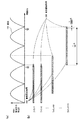
ここで、フリッカ発生の原理について図1〜図3を参照して説明する。ここでは、条件(1)の光源を電源周波数60Hzの蛍光灯(以下「60Hz蛍光灯」)とする。また、CMOS素子の水平ラインの数は1125本とする。 Here, the principle of flicker generation will be described with reference to FIGS. Here, the light source of the condition (1) is a fluorescent lamp with a power supply frequency of 60 Hz (hereinafter “60 Hz fluorescent lamp”). The number of horizontal lines of the CMOS element is 1125.
図1は、60Hz蛍光灯の下におけるCMOS素子の各水平ラインの露光のタイミングを示す図である。
図1(a)は、60Hz蛍光灯の明るさの時系列変化を示すグラフである。
縦軸は、60Hz蛍光灯の明るさを示す。横軸は、時間軸を表す。波形102からわかるように蛍光灯の明滅周期は、120Hzである。
FIG. 1 is a diagram showing the exposure timing of each horizontal line of a CMOS device under a 60 Hz fluorescent lamp.
Fig.1 (a) is a graph which shows the time-sequential change of the brightness of a 60 Hz fluorescent lamp.
The vertical axis indicates the brightness of the 60 Hz fluorescent lamp. The horizontal axis represents the time axis. As can be seen from the
図1(b)は、露光開始時間を示す図である。
前述の条件(2)を満たすようにするため、撮像素子で撮像する映像のフレームレートは60frames/secとする。つまり、1フレーム分の画像を撮像するのに必要な時間(露光時間)は1/60secである。また、CMOS素子に設定される条件(3)の電子シャッタのシャッタ速度は、1/2000secとする。
FIG. 1B shows the exposure start time.
In order to satisfy the above condition (2), the frame rate of the video imaged by the image sensor is 60 frames / sec. That is, the time (exposure time) required to capture an image for one frame is 1/60 sec. The shutter speed of the electronic shutter under the condition (3) set for the CMOS element is set to 1/2000 sec.
以上のような条件で撮像すると、CMOS素子の各水平ライン(水平ライン1〜水平ライン1125)の1フレーム分の露光時間である1/60secの内、実際に使用する映像は有効露光時間103の1/2000secのみとなる。つまり、無効露光時間104の映像は使用されない。
When imaging is performed under the above conditions, an image actually used has an effective exposure time of 103 within 1/60 sec which is the exposure time of one frame of each horizontal line (
また、CMOS素子の各水平ラインの露光は、水平ライン1〜水平ライン1125の順で行われていく。これが、1フレームの画像を撮像する手順に相当する。そして、1フレームの画像を撮像し終えると、また水平ライン1が露光される。1フレーム(1125本の水平ライン)分の画像を1/60secで撮像するために、隣接する各水平ライン間の露光開始のタイミングのずれは1/60÷1125secとなっている。
Further, exposure of each horizontal line of the CMOS element is performed in the order of
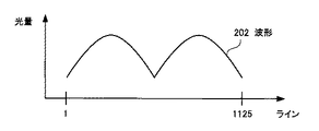
このように60Hz蛍光灯下において、電子シャッタのシャッタ速度を1/2000secと設定して撮像を行った場合、撮像素子の各水平ラインに入ってくる光量は、波形102を各水平ラインの有効露光時間103で積分することにより算出できる。この光量の各水平ラインの変動は、図2に示す波形202のようになり、蛍光灯の明滅周期と等しく120Hzとなる。
In this way, when imaging is performed with the shutter speed of the electronic shutter set to 1/2000 sec under a 60 Hz fluorescent lamp, the amount of light entering each horizontal line of the image sensor is represented by the
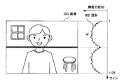
実際、60Hzの蛍光灯の下において、電子シャッタのシャッタ速度1/2000secで所定の撮像対象物を撮像した場合、CMOS素子の各水平ラインに入ってくる光は撮像対象物からの反射光である。そのため、図3に示す撮像される所定の1フレームの画像303は、動かない120Hz周期の明暗の縞模様が生じたものとなる。すなわち、画像303の水平ラインの輝度変動は、波形302のようにフリッカに起因する周期的な変動の上に撮像対象物に起因する変動が乗ったものとなる。このような動かないフリッカの場合、現在のフレームを構成する各画素の輝度と前フレームを構成する同一の各画素との間に、蛍光灯の明滅に起因する輝度の変動はあまり生じない。 Actually, when a predetermined imaging object is imaged at a shutter speed of 1/2000 sec under a 60 Hz fluorescent lamp, the light entering each horizontal line of the CMOS element is reflected light from the imaging object. . Therefore, a predetermined one-frame image 303 to be imaged shown in FIG. 3 is a non-moving 120 Hz period light and dark stripe pattern. In other words, the luminance fluctuation of the horizontal line of the image 303 is obtained by adding the fluctuation caused by the imaging target to the periodic fluctuation caused by flicker like the waveform 302. In the case of such flicker that does not move, there is not much fluctuation in luminance due to the blinking of the fluorescent lamp between the luminance of each pixel constituting the current frame and the same pixel constituting the previous frame.
ところで、フリッカの補正を行なう代表的な技術としては、フレームまたはフィールド周波数と放電等の明滅周波数によって決まるうなりにより発生した画面内の輝度及び色相変換の波形を用いて輝度および色信号の利得を制御する補正値を作成し、各信号の利得を制御することによりフリッカを制御する技術が開示されている(例えば、特許文献1を参照)。
特許文献1に記載された技術は、動くフリッカの制御はできるものの、動かないフリッカに対してフリッカ補正が行なえないという問題があった。
Although the technique described in
本発明は斯かる点に鑑みてなされたものであり、動かないフリッカが発生した映像からフリッカを除去(抑圧)することを目的とする。 The present invention has been made in view of such a point, and an object thereof is to remove (suppress) flicker from an image in which flicker that does not move occurs.
上記課題を解決するため、本発明による撮像装置は、所定のフレームレートおよび水平ライン総数に基づくタイミングで動作し、シャッタ速度を設定可能な電子シャッタを備え、該電子シャッタのシャッタ速度に応じた期間における入射光を、水平ライン毎に光電変換して所定の信号を生成する撮像素子と、撮像素子で生成された信号のゲインを調整して所定のレベルの信号を生成して映像信号を生成するゲイン調整回路と、入射光の明滅周期がフレームレートの整数倍であり、かつ電子シャッタに所定のシャッタ速度が設定されているときにゲイン調整回路で生成される映像信号と、入射光の明滅周期がフレームレートの整数倍であり、かつ電子シャッタに入射光の明滅周期の整数倍のシャッタ速度が設定されているときにゲイン調整回路で生成される、フリッカの発生しない基準映像信号を比較し、映像信号に含まれる、該映像信号で表される画像の垂直方向のフリッカ成分を算出し、該算出結果に応じて映像信号に含まれるフリッカを除去する補正回路とを有するものである。 In order to solve the above-described problem, an imaging apparatus according to the present invention includes an electronic shutter that operates at a timing based on a predetermined frame rate and the total number of horizontal lines and can set a shutter speed, and has a period according to the shutter speed of the electronic shutter. An image sensor that photoelectrically converts incident light at each horizontal line to generate a predetermined signal, and adjusts the gain of the signal generated by the image sensor to generate a signal of a predetermined level to generate a video signal A gain adjustment circuit, a video signal generated by the gain adjustment circuit when the blinking cycle of incident light is an integral multiple of the frame rate, and a predetermined shutter speed is set for the electronic shutter, and the blinking cycle of incident light Is an integer multiple of the frame rate, and the gain adjustment circuit when the electronic shutter is set to a shutter speed that is an integral multiple of the blinking cycle of the incident light The generated reference video signal that does not generate flicker is compared, and the vertical flicker component of the image represented by the video signal is calculated and included in the video signal according to the calculation result. And a correction circuit for removing flicker.
上記構成によれば、先にフリッカを含まない基準映像信号を生成しておき、当該基準映像信号とフリッカを含む映像信号との比較を行う。そして、この比較結果に基づいて、映像信号に含まれるフリッカの特徴を示すフリッカ成分を生成するようにした。これにより、映像信号に含まれるフリッカの特徴を知ることができるようになり、当該映像信号に含まれるフリッカを除去(抑圧)することができる。 According to the above configuration, a reference video signal that does not include flicker is generated in advance, and the reference video signal is compared with a video signal that includes flicker. Based on the comparison result, a flicker component indicating the flicker feature included in the video signal is generated. Thereby, it becomes possible to know the characteristics of the flicker included in the video signal, and it is possible to remove (suppress) the flicker included in the video signal.
本発明によれば、映像信号に含まれるフリッカの特徴を知ることができる。これにより、容易に当該映像信号に含まれるフリッカの除去(抑圧)を行うことができる。 According to the present invention, it is possible to know the characteristics of flicker included in a video signal. Thereby, it is possible to easily remove (suppress) the flicker included in the video signal.
以下、本発明の一実施形態の例について図4〜図14を参照して説明する。 Hereinafter, an example of an embodiment of the present invention will be described with reference to FIGS.
以下に述べる実施の形態は、本発明の好適な具体例であるから、技術的に好ましい種々の限定が付されているが、本発明の範囲は、下記の説明において特に本発明を限定する旨の記載がない限り、これらの形態に限られるものではない。例えば、以下の説明で挙げる各パラメータの数値的条件は好適例に過ぎず、説明に用いた各図における寸法、形状および配置関係も概略的なものである。 Since the embodiments described below are preferable specific examples of the present invention, various technically preferable limitations are given, but the scope of the present invention is particularly limited in the following description. Unless otherwise stated, the present invention is not limited to these forms. For example, the numerical conditions of each parameter given in the following description are only suitable examples, and the dimensions, shapes, and arrangement relationships in the drawings used for the description are also schematic.
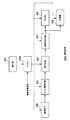
図4は、本例の撮像装置を示す機能ブロック図である。
図4に示す撮像装置401は図示しないレンズを有し、このレンズを介して撮像光が撮像素子404の図示しない撮像面に結像される。撮像素子404は、CMOS(complementary metal oxide silicon)素子であり、レンズ1を介して結像された撮像光を水平ライン毎に所定のタイミングで光電変換して所定のアナログ信号を生成する。そして、撮像素子404で生成されたアナログ信号はゲイン調整回路405に供給される。また、この撮像素子404は、電子シャッタ機能を有しており、後述するマイコン402からの指示に基づいて、電子シャッタのシャッタ速度を決定する。なお、本例では、撮像素子404で撮像された映像のフレームレートが60frames/secであるとし、撮像素子404の水平ラインの数が1125であるとする。
FIG. 4 is a functional block diagram illustrating the imaging apparatus of this example.
An imaging apparatus 401 illustrated in FIG. 4 includes a lens (not illustrated), and imaging light is imaged on an imaging surface (not illustrated) of the
ゲイン調整回路405は、撮像素子404から供給されるアナログ信号のゲインを調節することにより所定のレベルのアナログ信号を生成し、生成したアナログ信号に対しA/D変換を行い、所定の映像信号を生成する回路である。ゲイン調整回路405で生成された映像信号は補正回路406に供給される。なお、本例では撮像素子404から供給されるアナログ信号のゲインを調整するとしたが、当該アナログ信号がA/D変換された後のデジタル信号のゲインを調整してもよい。
The
補正回路406は、ゲイン調整回路405から供給される映像信号に含まれるフリッカの除去(抑圧)を行う(以下、「フリッカ補正処理」という)回路である。
The
フリッカ補正処理された映像信号は、画像処理回路407に供給される。本発明の本質ではないが、補正回路406では、各々画像データの周辺光量落ちの補正処理、所定の補間処理、それに伴うフィルタ処理、シェーディング補正処理などの信号処理を行い、さらに画質の向上を図るような処理等も行われる。これら補正回路406でのフリッカ補正処理およびその他の補正処理は、マイコン402からの制御に基づいて行われる。なお、補正回路406の詳細については、図5〜図14にて後述する。
The video signal subjected to the flicker correction process is supplied to the
画像処理回路407は、補正回路406から供給される映像信号に対して、色調調整処理、輝度圧縮処理、ガンマ補正等の周知の画像処理を行う回路である。そして、このような画像処理のなされた映像信号は、液晶ディスプレイ等からなる表示部408に映像として映し出される他、例えばメモリ等で構成される記録部409に記録される。
The
マイクロコンピュータ402(以下、「マイコン402」という。)は、制御部の一例であり、撮像装置401を構成する各回路を制御する。より具体的には、マイコン402は、撮像素子404の電子シャッタに関するシャッタ速度の設定およびゲイン調整回路405に関するゲインの設定等を制御するとともに、設定したシャッタ速度およびゲインに応じて、図5にて後述する補正回路406の各ブロックを制御する。
A microcomputer 402 (hereinafter referred to as “
また、マイコン402は、図示しないレンズ等の光学系、撮像素子404等の各部の動作を制御する。操作部403は、撮像装置401に配設されたボタンキーや当該撮像装置401に搭載された表示部408の画面に表示されるアイコンに割り当てられたソフトキー等からなり、操作に応じた操作信号が図示しないインターフェースを介して操作部403からマイコン402に入力される。マイコン402は、利用者が操作部403を操作して入力した操作信号、もしくは予め規定された設定等に基づいて、内蔵のROM(Read Only Memory)等の不揮発性記憶部に記録されているコンピュータプログラムに従い、所定の演算および各回路に対する制御を行う。
The
操作部403を通じてユーザからの基準値取り込み指示があった場合、マイコン402は、ゲイン調整回路405で生成される映像信号で表される画像の垂直方向にフリッカが出ないようなシャッタ速度およびゲインを撮像素子404の電子シャッタおよびゲイン調整回路にそれぞれ設定する。本例では、このようなシャッタ速度およびゲインを基準シャッタ速度および基準ゲインと定義する。また、電子シャッタに設定されたシャッタ速度が基準シャッタ速度であり、かつゲイン調整回路405に設定されたゲインが基準ゲインである場合に、ゲイン調整回路405で生成される映像信号を基準映像信号と呼ぶ。なお、基準映像信号の具体的な生成方法については、図9および図10にて後述する。
When there is a reference value capture instruction from the user through the
次に、補正回路406について詳細な説明を行う。
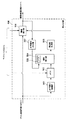
図5は、本例の撮像装置401の補正回路406を示すブロック図である。
図5に示す補正回路406の第一水平積分処理部502は、ゲイン調整回路405から供給される基準映像信号を利用して、当該基準信号で表される画像の各水平ラインを構成する画素の輝度の総和(以下、「基準値」という。)を算出するものである。算出した基準値はメモリ503に記憶される。
Next, the
FIG. 5 is a block diagram illustrating the
The first horizontal
一方、第二水平積分処理部507は、ゲイン調整回路405を通じて振幅補正部506で補正された映像信号を利用して、当該映像信号で表される画像の各水平ラインを構成する各画素の輝度の総和(以下「撮像値」という。)を算出するものである。第二水平積分処理部507で算出された撮影値は相関検出部504に供給される。
On the other hand, the second horizontal
相関検出部504は、基準値をメモリ503から読み出し、撮像値と読み出した基準値との相関関係を同一水平ライン毎に検出するものである。具体的には、各水平ラインの基準値と各水平ラインの撮像値との差分である値(以下、「相関値」という。)を計算する。なお、相関値は撮像素子404の水平ラインの本数だけ値をもつ。
The
さらに、相関検出部504は、計算した相関値がもつ各値の総和(以下、「差分和」)を算出する。また、相関検出部504は、メモリ508を有しており、差分和をこのメモリ508に記憶する。相関検出部504は、メモリ508に差分和が記憶されているならば、この差分和を利用して、補正回路406から第二水平積分処理部507を通じて供給される、補正された映像信号の撮像値に対して、適切にフリッカ補正処理がなされているか否かを判断する。そして、判断結果に基づいて、補正値生成部505を制御する。
Further, the
補正値生成部505は、さまざまな、位相および振幅の正弦波形や半波整流波形などが記録されているROMテーブルを備えており、当該ROMテーブルを参照して所定の初期位相および初期振幅を持った初期波形(最初に生成される補正波形)を生成するものである。また、補正値生成部505は、相関検出部504の制御に基づいて、前回生成した補正波形の位相および振幅をそれぞれ所定の値だけ増減する。なお、この増減には、ROMテーブルが利用される。また、補正波形とは、映像信号からフリッカを除去(抑圧)するための「補正信号の波形」のことを指す。
The correction
振幅補正部506は、補正値生成部505にて生成される補正波形(補正信号)に基づいて、ゲイン調整回路405から供給される映像信号に対して所定の信号処理を行うものである。所定の信号処理とは、ゲイン調整回路405から供給される映像信号が、画像処理回路407を介して表示部408に供給された際に、この表示部408に映し出される映像にフリッカが生じないようにする処理のことである。より具体的には、フリッカを示す波形202(図2を参照)と逆相の波形である補正波形(補正信号)に基づいて、ゲイン調整回路405からの映像信号の振幅を調整することでフリッカを取り除き、光源からの明滅光の影響を排除した映像だけを取り出す処理のことである。振幅補正部506で補正された映像信号は、画像処理回路407および第二水平積分処理部507に供給される。
The
マイコン402からの基準値取り込み指示がある場合は、振幅補正部506はゲイン調整回路405から供給される映像信号に対して補正は行わず、当該映像信号がそのまま画像処理回路407へ供給される。さらに、この場合、マイコン402の制御により、振幅補正部506から第二水平積分処理部507への映像信号の供給は行われない。
When there is a reference value fetch instruction from the
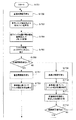
[一実施形態に係る撮像装置の動作]
次に、図6を参照して、撮像装置401を構成する各機能ブロックにおける処理の流れについて説明を行う。
図6は、撮像装置401の動作を示すフローチャートである。
ビデオ装置による撮像中にシャッタ速度およびゲインを変更する場合、ユーザは操作部403に対し所定の操作を行う。すると、マイコン402を通じて、撮像素子404の電子シャッタおよびゲイン調整回路405に所定のシャッタ速度および基準ゲインがそれぞれ設定される。(ステップS601)。以下では、このステップS601の処理でユーザの設定したシャッタ速度およびゲインをそれぞれ「撮像用シャッタ速度」および「撮像用ゲイン」という。
[Operation of Imaging Device According to One Embodiment]
Next, with reference to FIG. 6, the flow of processing in each functional block constituting the imaging apparatus 401 will be described.
FIG. 6 is a flowchart showing the operation of the imaging apparatus 401.
When changing the shutter speed and gain during imaging by the video apparatus, the user performs a predetermined operation on the
ここで、ユーザは、現在撮影中の映像にフリッカがあるか否かを表示部408にて目視確認する(S602)。そして、ユーザはフリッカの補正を行うか否かを決定する(ステップS603)。フリッカの補正を行わないならば、ステップS602の処理に戻る(ステップS603のNO)。フリッカの補正を行うならば(ステップS603のYES)、ユーザは操作部403に対し所定の操作を行うと、マイコン402に前述の基準値取り込み指示が供給される。
Here, the user visually checks on the
そして、この基準値取り込み指示をトリガーにして、マイコン402により基準シャッタ速度および基準ゲインが撮像素子404の電子シャッタおよびゲイン調整回路405にそれぞれ設定される(ステップS604)。
Then, using this reference value fetch instruction as a trigger, the
ここで、基準シャッタ速度および基準ゲインの具体例について説明する。撮像した映像にフリッカが出ないシャッタ速度は、前述の条件(2)より蛍光灯の明滅周期の整数倍である。本例では、基準シャッタ速度を1/60secとする。また、基準ゲインは、マイコン402により、基準シャッタ速度×基準ゲインが撮像用シャッタ速度×撮像用ゲインと等しくなるように設定される。なお、電子シャッタのシャッタ速度1/60secとは、当該電子シャッタを使用しない状態に等しい。
Here, specific examples of the reference shutter speed and the reference gain will be described. The shutter speed at which flicker does not appear in the captured image is an integral multiple of the blinking cycle of the fluorescent lamp based on the condition (2). In this example, the reference shutter speed is 1/60 sec. The reference gain is set by the
図6の説明に戻る。
ステップS604の処理が完了後、撮像素子404およびゲイン調整回路405を通じて、基準シャッタ速度で撮像された、基準ゲインが反映された映像信号(以下、「基準映像信号」という。)が第一水平積分処理部502に供給される。そして、基準映像信号の水平ライン毎の輝度の積分値が算出され(以下、「水平積分」という。)、基準映像信号の水平積分結果が基準値としてメモリ503に記憶される(ステップS605)。
Returning to the description of FIG.
After the processing in step S604 is completed, a video signal reflecting the reference gain (hereinafter referred to as “reference video signal”) captured at the reference shutter speed through the
ここで、現在撮像素子404およびゲイン調整回路405に設定されている、基準シャッタ速度および基準ゲインが、マイコン402の制御により撮像用シャッタ速度および撮像用ゲインに変更される(ステップS606)。
Here, the reference shutter speed and the reference gain that are currently set in the
すると、撮像素子404およびゲイン調整回路405を通じて、撮像用シャッタ速度で撮像された、撮像用ゲインに設定された映像信号(以下、「撮像用映像信号」という。)が振幅補正部506に供給される。そして、撮像用映像信号は、メモリ503に記憶された基準値に基づいて、フリッカ補正処理される(ステップS607)。なお、撮像用映像信号に対するフリッカ補正処理は、おもに第二水平積分処理部507、相関検出部504、補正値生成部505および振幅補正部506で行われるが、その詳細については図7および図8にて後述する。
Then, a video signal set to the imaging gain (hereinafter referred to as “imaging video signal”) captured at the imaging shutter speed is supplied to the
ステップS607の処理が完了後、マイコン402は、ユーザによる操作部403からのフリッカ補正処理の停止指示があるか否かを確認する(ステップS608)。停止指示があるならば(ステップS608のNO)、ステップS602の処理に戻り、ステップS602以降の処理を繰り返す。停止指示がないならば(ステップS608のYES)、マイコン402はユーザによる操作部403からの基準値再取得の指示、すなわち基準値取り込み指示があるか否かを確認する(ステップS609)。基準値取り込み指示がないならば(ステップS609のNO)、撮像用映像信号は同じ基準値に基づいたフリッカ補正処理がなされる(ステップS607)。
After the process of step S607 is completed, the
基準値取り込み指示があるならば(ステップS609のYES)、ステップS604の処理に戻り、再度基準値を取得する。 If there is a reference value import instruction (YES in step S609), the process returns to step S604 to acquire the reference value again.
[フリッカ補正処理]
図7および図8は、図6のステップS607の処理である、フリッカ補正処理の詳細な処理の流れを示すフローチャートである。以下、第二水平積分処理部507、相関検出部504、補正値生成部505および振幅補正部506が行うフリッカ補正処理について説明する。
[Flicker correction processing]
7 and 8 are flowcharts showing a detailed flow of the flicker correction process, which is the process of step S607 in FIG. Hereinafter, the flicker correction processing performed by the second horizontal
まず、フリッカ補正処理を開始すると(ステップS701)、マイコン402はカウンタを構成する変数iを0に初期化する(ステップS702)。変数iは、映像信号で表される所定の1フレームの画像の水平ラインの番号を示すものである。
First, when flicker correction processing is started (step S701), the
マイコン402は、ゲイン調整回路405から振幅補正部506へ供給されている撮像用映像信号で表される画像が、1フレーム目のものであるか否かを確認する(ステップS703)。1フレーム目の画像であるならば(ステップS703のYES)、振幅補正部506は初期波形で当該撮像用信号の振幅補正を行う(ステップS704)。なお、初期波形は、補正値生成部505によって生成される。ただし、本例では、初期波形は、所定の初期位相および初期振幅を持つ波形とする。
The
以上の処理が完了後、マイコン402は変数iをインクリメントする(ステップS705)。そして、第二水平積分処理部507は、映像信号で表される1フレーム目の画像のi番目の水平ラインを水平積分することでi番目の水平ラインの輝度の総和を算出する(ステップS706)。そして、相関検出部504は、i番目の水平ラインの水平積分結果(前述のi番目の水平ライン目の撮像値)と、当該水平積分結果を算出した水平ラインと同一の水平ラインの基準値とを比較し、差分(前述のi番目の水平ライン目の相関値)を算出する(ステップS707)。そして、相関検出部504は、差分を順次加算し、差分和を算出する(ステップS708)。つまり、1回目のループでは、1番目の水平ラインに対応する、撮像値と基準値との差分が差分和となる。2回目のループでは、1回目のループの差分和に2番目の水平ラインに対応する、撮像値と基準値との差分を加算したものが、差分和となる。3回目のループでは、2回目のループの差分和に3番目の水平ラインに対応する、撮像値と基準値との差分を加算したものが、差分和となる。
After completing the above processing, the
以上の処理が完了後、相関検出部504は、1フレーム分、すなわち1125本の各水平ラインの差分(相関値)の加算が終了したか否かを確認する(ステップS709)。終了していない、すなわち現在の変数iが1125よりも小さいならば(ステップS709のNO)、ステップS705の処理に戻る。
After the above processing is completed, the
終了している、すなわち現在の変数iが1125以上であるならば(ステップS709のYES)、相関検出部504は、ステップS705〜ステップS708のループ処理で算出された差分和を自身に備えるメモリ508に記憶する(ステップS710)。
If completed, that is, the current variable i is 1125 or more (YES in step S709), the
ここで、補正値生成部505は、相関検出部504の制御に基づいて、初期波形(補正波形)の補正を行なう(ステップS711)。ここでの相関制御部504の制御とは、補正値生成部505で補正する、初期波形の位相および振幅それぞれを増減させる方向(+/−)を適当な方向に決定することである。
Here, the correction
そして、振幅補正部506は、補正値生成部505で補正された補正波形に基づいて、ゲイン調整回路405から供給される撮像用映像信号を補正し(ステップS712)、図6のステップS608の処理に戻る(ステップS713)。
Then, the
一方、撮像用映像信号で表される画像が、2フレーム目以降のものであるならば(ステップS703のNO)、振幅補正部506は、前回補正値生成部505で生成された補正波形に基づいて、振幅補正を行う(ステップS801)。
On the other hand, if the image represented by the imaging video signal is the second and subsequent frames (NO in step S703), the
そして、マイコン402は変数iをインクリメントする(ステップS802)。そして、第二水平積分処理部507は映像信号で表される所定番目(2番目以降)のフレームの画像のi番目の水平ラインを水平積分し、i番目の水平ラインの輝度の総和(i番目のラインの撮像値)を算出する(ステップS803)。そして、相関検出部504は、i番目の水平ラインの水平積分結果と、当該水平積分結果を算出した水平ラインと同一の水平ラインの基準値とを比較し、差分(i番目の水平ラインの相関値)を算出する(ステップS804)。そして、相関検出部504は、差分を順次加算し、差分和を算出する(ステップS805)。つまり、1回目のループでは、1番目の水平ラインに対応する、撮像値と基準値との差分が差分和となる。2回目のループでは、1回目のループの差分和に2番目の水平ラインに対応する、撮像値と基準値との差分を加算したものが、差分和となる。3回目のループでは、2回目のループの差分和に3番目の水平ラインに対応する、撮像値と基準値との差分を加算したものが、差分和となる。
Then, the
以上の処理が完了後、相関検出部504は、1フレーム分、すなわち1125本の各水平ラインの差分(相関値)の加算が終了したか否かを確認する(ステップS806)。終了していない、すなわち現在の変数iが1125よりも小さいならば(ステップS806のNO)、ステップS802の処理に戻る。
After the above processing is completed, the
1フレーム分の各水平ラインの差分(相関値)の加算が終了している、すなわち現在の変数iが1125以上であるならば(ステップS806のYES)、相関検出部504は、メモリ508に記憶された、1フレーム前の差分和と、今フレームの差分和とを比較する(ステップS807)。そして、今フレームの差分和が、1フレーム前の差分和よりも大きいか否かを確認する(ステップS808)。今フレームの差分和が1フレーム前の差分和よりも大きい場合は(ステップS808のYES)、相関検出部504は、1フレーム前に生成した補正波形の位相および振幅を変化させる指示を補正値生成部505へ出力する(ステップS809)。そして、相関検出部504は、メモリ508に記憶されている差分和を今フレームの差分和に更新する(ステップS810)。そして、補正値生成部505は、相関検出部504からの指示に基づいて、補正信号の位相および振幅を決定する(ステップS813)。
If the addition of the difference (correlation value) of each horizontal line for one frame has been completed, that is, if the current variable i is 1125 or more (YES in step S806), the
一方、今フレームの差分和が1フレーム前の差分和以下の場合は(ステップS808のNO)、相関検出部504は、1フレーム前の補正波形の位相変化方向および振幅増減方向をそのままに保つ指示を補正値生成部505へ出力する。ここで、メモリ508に記憶されている差分和を今フレームの差分和に更新する(ステップS812)。そして、ステップS813の処理に移行し、補正値生成部505は、相関検出部504からの指示に基づいて補正波形の位相および振幅を決定する(ステップS813)。
On the other hand, if the difference sum of the current frame is equal to or less than the difference sum of the previous frame (NO in step S808), the
以上の処理が完了後、補正値生成部505は、相関検出部504で決定された、位相および振幅の補正波形を生成する(ステップS814)。そして、振幅補正部506は、補正値生成部505にて生成された補正波形に基づいて、ゲイン調整回路405から供給される撮像用映像信号を補正し(ステップS815)、図6のステップS608の処理に戻る(ステップS816)。
After the above processing is completed, the correction
以上の、ステップS808〜ステップS813の処理で行われる補正波形の位相および振幅の補正についてさらに詳細に説明する。
相関検出部504では、補正後の映像が基準映像にどこまで近づいたかを見るための差分和を検出する。そして、相関検出部504はこの差分和から相関の強弱を判断し補正方針(位相の変化方向、振幅の増減方向)が間違っていないかを判断する。前回の補正がその前の補正よりも差分和が大きくなり相関が弱くなったと判断すれば、補正方針が間違っていたとして、今回の補正では補正対象である補正波形の位相変化の方向や振幅の増減方向を逆にする。逆に前回の補正がその前の補正よりも差分が小さくなっていれば、補正方針は合っていたものとして、今回の補正では補正対象の補正波形の位相、振幅の増減方向はそのままにする。その結果として、相関検出部504は、補正信号の位相と振幅それぞれの増減方向(+/−)を変化させる制御信号を生成し、生成した制御信号を補正値生成部505に出力することになる。
The correction of the phase and amplitude of the correction waveform performed in the above-described processing in steps S808 to S813 will be described in more detail.
The
そして、補正値生成部505は、相関検出部504から入力された制御信号に基づいて生成する補正波形の位相、振幅を修正(変化)する。これにより、補正波形は、徐々に差分和の小さくなる方へ補正されていき、結果として映像信号に重畳されているフリッカ成分を反転(天地逆)したものに近づいていく。
Then, the correction
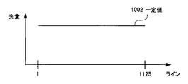
図9は、マイコン402から撮像素子404に前述の基準値取り込み指示があった場合、撮像素子404の各水平ラインに入る撮像光を示す図である。
図9(a)は、60Hz蛍光灯の明るさの時系列変化を示すグラフである。
縦軸は、60Hz蛍光灯の明るさを示す。横軸は、時間軸を表す。波形902からわかるように蛍光灯の明滅周期は、120Hzである。
FIG. 9 is a diagram illustrating imaging light that enters each horizontal line of the
FIG. 9A is a graph showing a time-series change in brightness of a 60 Hz fluorescent lamp.
The vertical axis indicates the brightness of the 60 Hz fluorescent lamp. The horizontal axis represents the time axis. As can be seen from the waveform 902, the blinking cycle of the fluorescent lamp is 120 Hz.
図9(b)は、前述の基準シャッタ速度と水平ラインとの時間的な関係を示す図である。
前述のように、撮像素子404で撮像する映像のフレームレートは60frames/secである。つまり、1フレーム目の画像を撮像するのに必要な時間は1/60secとなる。撮像素子404の電子シャッタを使用しない、すなわちシャッタ速度が1/60secの場合、撮像素子404の各水平ラインの露光時間903は1/60sec間隔となる。前述したが、この1/60secという露光時間903は、60Hzの蛍光灯下においては撮像する映像にフリッカが発生しない露光時間(前述の基準シャッタ速度)である。
FIG. 9B is a diagram showing a temporal relationship between the reference shutter speed and the horizontal line.
As described above, the frame rate of an image captured by the
撮像素子404の各水平ラインの露光開始のタイミングは異なっており、本例のように撮像する映像のフレームレートが60frames/secであり、かつ撮像素子404の水平ラインの数が1125ある場合、隣接する各水平ライン間の露光開始時間のずれは1/60÷1125secとなる。
The exposure start timing of each horizontal line of the
以上のように電子シャッタのシャッタ速度を1/60secと設定して撮像を行った場合、撮像素子404の各水平ラインに入ってくる蛍光灯照明下での光量(以下、「蛍光灯下光量」という。)は、波形902を各水平ラインの露光時間903で積分することにより算出できる。この蛍光灯光下量は、図10に示すように水平ラインによらず一定値1002をとる。
As described above, when imaging is performed with the shutter speed of the electronic shutter set to 1/60 sec, the amount of light under the fluorescent lamp illumination that enters each horizontal line of the image sensor 404 (hereinafter, “the amount of light under the fluorescent lamp”). Can be calculated by integrating the waveform 902 with the exposure time 903 of each horizontal line. As shown in FIG. 10, the amount of light under the fluorescent lamp takes a
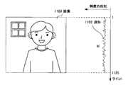
つまり、60Hzの蛍光灯の下、シャッタ速度1/60secで所定の撮像対象物を撮像したならば、図11のような、フリッカの発生していない1フレームの画像1103を取得することとなる。この画像1103が、基準映像信号で表される画像である。 That is, if a predetermined imaging object is imaged under a 60 Hz fluorescent lamp at a shutter speed of 1/60 sec, one frame image 1103 in which flicker is not generated as shown in FIG. 11 is acquired. This image 1103 is an image represented by the reference video signal.
画像1103の各水平ラインの輝度は、蛍光灯下光量(図10の一定値1002)が撮像対象物に反射した反射光量で決定されるので、波形1102のようになる。この波形1102が、図6のステップS605の処理にて、生成される基準値に相当する。本例では、波形1102をbiと定義する。なお、iはラインを示す変数である。
The luminance of each horizontal line of the image 1103 is as shown by a waveform 1102 because the amount of light under the fluorescent lamp (a
[フリッカ補正処理の概要]
次に、フリッカ補正処理のイメージについて図12〜図13を参照して説明する。
図3に示す、フリッカの発生している画像303に対しフリッカ補正処理を行う例について述べる。画像303は、60Hzの蛍光灯の下、電子シャッタのシャッタ速度1/2000secで撮像を行った場合、ゲイン調整回路405で生成される撮像用映像信号で表される画像である。このような画像303の各水平ラインの輝度は、蛍光灯下光量(図2の波形202)が撮像対象物に反射した反射光量で決定されるので、波形302のようになる。この波形302が、図8のステップS802〜ステップS805のループ処理で算出される撮像値に相当する。本例では、図3に示す波形302をaiと定義する。なお、iはラインを示す変数である。
[Overview of flicker correction processing]
Next, an image of the flicker correction process will be described with reference to FIGS.
An example in which flicker correction processing is performed on the flickered image 303 shown in FIG. 3 will be described. An image 303 is an image represented by an imaging video signal generated by the
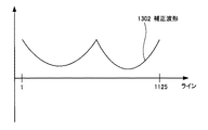
ところで本実施の形態において、相関検出部504では、図3に示す波形302(撮像値)と、図11に示す波形1102(基準値)との差分を計算、すなわち|ai−bi|を計算することで、相関値を生成している。この相関検出部で生成される相関値の絶対値をはずした波形を図12に示す。縦軸は輝度を示している。横軸は各水平ラインを表している。この波形1202が、表示部408に表示される画像のフリッカの形状を示す波形(以下、「フリッカ成分」という)である。すなわち、相関値は、広い意味で表示部に表示される画像のフリッカの形状を示す値である。
In the present embodiment, the
そして、相関検出部504は、相関値から前述の差分和を算出し、当該差分和をメモリ508に記憶する。ここで、メモリ508に記憶する差分和を計算する式を以下に示す。
Then, the
(差分和)=Σ|ai−bi| (Sum of differences) = Σ | a i −b i |
例えば、現在メモリ508に記憶された差分和が、nフレーム目の画像に対応する撮像用映像信号(以下、「nフレーム目の撮像用映像信号」という。)の相関値から算出したものであるとする。その場合、メモリ508に記憶された差分和は、n+1フレーム目の撮像用映像信号の撮影値が相関検出部504に入力された際に、当該n+1フレーム目の撮像用映像信号に適切なフリッカ補正処理がなされているか否かの判断と、補正値生成部505に対して補正波形の位相および振幅の増減指示を行うのに利用される。この増減指示を行うことが、図8のステップS813の処理に相当する。
For example, the difference sum currently stored in the
補正値生成部505は、相関検出部504から供給される位相および振幅の増減指示に基づいて、補正波形を補正する。ここで、フリッカを取り除くために理想的な補正波形を図13に示す。縦軸は振幅を示している。横軸は撮像素子404の各水平ラインを表している。図12の波形と逆相、すなわちフリッカに関係する光量の変動と逆相の波形が補正波形1302である。補正値生成部505は、相関検出部504からの指示に基づいてこのような補正波形1302に近づくように補正波形の位相および振幅を変化させる。このような処理が、図7のステップS711の処理および図8のステップS814の処理に相当する。
The correction
振幅補正部506では、補正値生成部505から供給される補正波形1302に基づいて、撮像用映像信号のフリッカ補正処理を行う。つまり、補正波形1302は、図3に示す画像302に発生しているフリッカによる輝度の変動とは逆相であるので、この補正波形1302を利用して撮像用映像信号に含まれるフリッカを取り除くことができる。このフリッカを取り除く処理が、図7のステップS712の処理および図8のステップS814の処理に相当する。
The
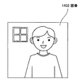
そして、フリッカ補正処理された撮像用映像信号が、画像処理回路407を通じて表示部408に入力される。すると、表示部408には、図14に示す、フリッカの除かれた画像1402が表示される。
Then, the imaging video signal subjected to the flicker correction process is input to the
以上のように、本実施形態では、フレーム毎に位相が動かないフリッカの位相の検出、当該フリッカの補正を容易に行うことができる。 As described above, in the present embodiment, it is possible to easily detect the phase of the flicker whose phase does not move for each frame and correct the flicker.
また、本実施形態では、ゲイン×電子シャッタのシャッタ速度が一定値になるように、マイコン402がゲイン調整回路405および撮像素子404を制御している。これにより、フレーム間の信号レベル変化を一定にすることができる。このため、基準値取り込み時に表示部408に表示される映像と、フリッカ補正処理後に表示部408に表示される映像の明るさが等しくなる。これにより、ユーザにとって見苦しくない映像が表示部408に表示される。
In the present embodiment, the
[他の実施形態]
[他の実施形態の撮像装置の構成]
以下、本発明の他の実施の形態の例について、図15〜図17を参照して説明する。
図15は、本例の撮像装置を示すブロック図である。
図16は、本例の撮像装置の補正回路を示すブロック図である。
撮像装置1501は、映像の記録指示があるまで、基準値の取り込みと、当該取り込んだ基準値を利用したフリッカ補正処理を1フレーム毎に交互に行うものである。このため、他の実施形態のマイコン1502は、ユーザによる操作部403からの記録指示があるまで、垂直同期信号を利用して1フレーム飛ばしのタイミングで前述の基準値取り込み指示を撮像素子404に供給する。なお、マイコン1502の他の機能は一実施形態のマイコン402と同じである。
[Other Embodiments]
[Configuration of Imaging Device of Other Embodiment]
Examples of other embodiments of the present invention will be described below with reference to FIGS.
FIG. 15 is a block diagram illustrating the imaging apparatus of this example.
FIG. 16 is a block diagram illustrating a correction circuit of the imaging apparatus of this example.
The imaging device 1501 alternately performs capture of a reference value and flicker correction processing using the captured reference value for each frame until a video recording instruction is issued. For this reason, the
マイコン1502以外の撮像装置1501の構成は、図4および図5に示す一実施形態の撮像装置401の構成と同じなので、説明は省略する。
Since the configuration of the imaging apparatus 1501 other than the
[他の実施形態の撮像装置の動作]
次に、図17を参照して撮像装置1501を構成する各機能ブロックにおける処理の流れを説明する。
図17は、撮像装置1501の動作を示すフローチャートである。
まず、ユーザは、撮像装置1501の電源を入れ、シャッタ速度およびゲインの設定を行う。具体的には、マイコン1502が、ユーザの操作部403に対する操作に基づいて、撮像素子404およびゲイン調整回路405に前述の、撮像用シャッタ速度および撮像用ゲインを設定する(ステップS1701)。
[Operation of Imaging Device of Other Embodiment]
Next, the flow of processing in each functional block constituting the imaging device 1501 will be described with reference to FIG.
FIG. 17 is a flowchart showing the operation of the imaging apparatus 1501.
First, the user turns on the imaging device 1501 and sets the shutter speed and gain. Specifically, the
ここで、マイコン1502は、図示しない同期信号発生部から供給される垂直同期信号を待つ(ステップS1702)。そして、マイコン1502の垂直同期信号が供給されると、マイコンは前述の基準値取り込み指示があるものと認識する。そして、当該マイコン1502により撮像素子404およびゲイン調整回路405に基準シャッタ速度および基準ゲインがそれぞれ設定される(ステップS1703)。
Here, the
そして、基準シャッタ速度で撮像された、基準ゲインに設定された、基準映像信号が第一水平積分処理部502に供給される。そして、基準映像信号で表される画像の各水平ラインの輝度の積分値が算出され、この積分値が基準値としてメモリ503に記憶される(ステップS1704)。
Then, the reference video signal, which is captured at the reference shutter speed and set to the reference gain, is supplied to the first horizontal
ここで、現在撮像素子404およびゲイン調整回路405に設定されている、基準シャッタ速度および基準ゲインが、マイコン1502の制御により撮像用シャッタ速度および撮像用ゲインに変更される(ステップS1705)。
Here, the reference shutter speed and the reference gain currently set in the
ここで、マイコン1502は、撮像中の映像を記録するか否かを確認する。すなわち、マイコン1502は、ユーザからの指示部に対する記録開始指示があるか否かを確認する(ステップS1706)。記録開始指示がない場合は(ステップS1706のYES)、マイコン1502は図示しない同期信号発生部からの垂直同期信号を待つ(ステップS1707)。
Here, the
そして、マイコン1502に垂直同期信号が供給されると、当該マイコン1502の制御により前述の撮像用映像信号が振幅補正部506に供給される。すると、撮像用映像信号は、メモリ503に記憶された基準値に基づいたフリッカ補正処理がなされる(ステップS1708)。
When the vertical synchronization signal is supplied to the
以上の処理が完了後、ステップS1702の処理に戻り、ステップS1702以降の処理を繰り返す。 After the above processing is completed, the processing returns to step S1702 and the processing after step S1702 is repeated.
一方、記録開始指示がある場合は(ステップS1706のNO)、マイコン1502は図示しない同期信号発生部からの垂直同期信号を待つ(ステップS1709)。そして、マイコン1502に垂直同期信号が供給されると、当該マイコン1502の制御により前述の撮像用映像信号が振幅補正部506に供給される。すると、撮像用映像信号は、メモリ508に記憶された基準値に基づいたフリッカ補正処理がなされる(ステップS1710)。そして、マイコン1502の制御により、フリッカ補正処理がなされた撮像用映像信号は画像処理回路407を通じて記録部409に記録されるとともに、表示部408に表示される。
On the other hand, if there is a recording start instruction (NO in step S1706), the
以上の処理が完了後、マイコン1502は、今記録部409に記録中の撮像用映像信号の記録を継続するか否かを確認する、すなわちマイコン1502は、ユーザからの指示部に対する記録終了指示があるか否かを確認する(ステップS1712)。記録終了指示がない場合は(ステップS1712のNO)、ステップS1709の処理に戻り、ステップS1709以降の処理を繰り返す。記録終了指示がある場合は(ステップS1712のYES)、ステップS1702の処理に戻り、ステップS1702以降の処理を繰り返す。なお、ステップS1708およびステップS1710の処理は、図6のステップS607の処理、すなわちフリッカ補正処理であり、その詳細な処理の流れは図7および図8のフローチャートで示したものと同じである。
After the above processing is completed, the
以上のように、本実施形態では、上記した一実施形態と同様に、フレーム毎に位相が動かないフリッカの位相の検出、当該フリッカの補正を容易に行うことができる。 As described above, in this embodiment, similarly to the above-described embodiment, it is possible to easily detect the flicker phase in which the phase does not move for each frame and correct the flicker.
さらに、本実施形態では、垂直同期信号を利用することで、基準値の生成と、当該基準値を利用したフリッカ補正処理とが、1フレーム毎に交互に行われる。そして、この1フレームおきのフリッカ補正処理は、撮像中の映像の記録が開始されるまで継続される。これにより、記録開始直前の補正波形の位相および振幅は補正に適切な状態に保たれることとなる。このような撮像中の映像の記録が開始された直後に算出した補正波形を利用して、記録部409に記憶する撮像用映像信号のフリッカ補正処理を行うことができる。これにより、より確実にフリッカを取り除くことができる。
Further, in the present embodiment, by using the vertical synchronization signal, the generation of the reference value and the flicker correction process using the reference value are alternately performed for each frame. Then, the flicker correction processing every other frame is continued until recording of the image being picked up is started. As a result, the phase and amplitude of the correction waveform immediately before the start of recording are maintained in a state appropriate for correction. By using the correction waveform calculated immediately after the recording of the image being captured is started, it is possible to perform the flicker correction processing of the imaging video signal stored in the
なお、上記した各実施形態では、60Hzで明滅する光源(蛍光灯)下において、60frames/secで撮像する撮像装置401を1/2000secという電子シャッタのシャッタ速度で動作させる場合に生じるフリッカの補正について説明した。しかし、50Hzで明滅する光源下において、50frames/secで撮像する撮像装置401を任意のシャッタ速度で動作させた場合に生じるフリッカについても補正を行うことができる。すなわち、明滅周期とフレームレートが等しい場合に生じるフリッカの補正を確実に行うことができる。 In each of the embodiments described above, correction of flicker that occurs when the imaging apparatus 401 that captures images at 60 frames / sec is operated at a shutter speed of 1/2000 sec under a light source (fluorescent lamp) that blinks at 60 Hz. explained. However, it is possible to correct flicker that occurs when the imaging device 401 that captures images at 50 frames / sec is operated at an arbitrary shutter speed under a light source that blinks at 50 Hz. That is, it is possible to reliably correct flicker that occurs when the blinking cycle and the frame rate are equal.
なお、上記の各実施形態では、輝度を利用してフリッカを取り除くための補正波形を算出した。しかし、例えばR(赤)、G(緑)、B(青)といった色信号に対しフリッカ補正を行う場合においても、色信号の信号レベルを輝度の場合と同様に処理することで補正波形を算出することができる。蛍光灯の発光特性、残光特性が色によって異なる場合があるが、このような場合でも取り込んだ映像に含まれる動かないフリッカを取り除くことができる。 In each of the above embodiments, a correction waveform for removing flicker is calculated using luminance. However, even when flicker correction is performed on color signals such as R (red), G (green), and B (blue), for example, a correction waveform is calculated by processing the signal level of the color signal in the same manner as in the case of luminance. can do. The light emission characteristics and afterglow characteristics of the fluorescent lamp may differ depending on the color. Even in such a case, it is possible to remove the non-moving flicker included in the captured image.
また、上記の各実施形態では、毎フレームについて補正波形の振幅および位相の増減方向を決定した。しかし、補正波形の位相の増減方向を毎フレーム決定し、補正波形の振幅の増減方向を例えば5フレーム毎に決定するようにしてもよい。このように、補正波形の位相の増減方向を決定する間隔と、補正波形の振幅の増減方向を決定する間隔を異なるようにすることで、位相と振幅の収束の優先度に差ができ、動作が安定する。 Further, in each of the above embodiments, the increase / decrease direction of the amplitude and phase of the correction waveform is determined for each frame. However, the increase / decrease direction of the phase of the correction waveform may be determined every frame, and the increase / decrease direction of the amplitude of the correction waveform may be determined every 5 frames, for example. In this way, by making the interval for determining the increase / decrease direction of the phase of the correction waveform different from the interval for determining the increase / decrease direction of the amplitude of the correction waveform, the priority of convergence of the phase and amplitude can be changed, and the operation Is stable.
以上、本発明の各実施形態の例について説明したが、本発明は上記各実施形態例に限定されるものではなく、本発明の要旨を逸脱しない限りにおいて、他の変形例、応用例を含むことはいうまでもない。 As mentioned above, although the example of each embodiment of the present invention was explained, the present invention is not limited to the above-mentioned each embodiment example, and includes other modification examples and application examples without departing from the gist of the present invention. Needless to say.
102…波形、103…有効露光時間、104…無効露光時間、202…波形、
302…波形、303…画像、401…撮像装置401、402…マイコン402、403…操作部403、404…撮像素子404、405…ゲイン調整回路405、406…補正回路406、407…画像処理回路407、408…表示部408、409…記録部409、502…第一水平積分処理部502、503…メモリ、504…相関検出部504、505…補正値生成部505、506…振幅補正部506、507…第二水平積分処理部507、508…メモリ、902…波形、903…露光時間、1002…一定量、1102…波形、1103…画像、1202…波形、1302…補正波形、1402…画像
102 ... Waveform, 103 ... Effective exposure time, 104 ... Invalid exposure time, 202 ... Waveform,
302 ... Waveform, 303 ... Image, 401 ...
Claims (12)
前記撮像素子で生成された信号のゲインを調整して所定のレベルの信号を生成して映像信号を生成するゲイン調整回路と、
前記入射光の明滅周期がフレームレートの整数倍であり、かつ前記電子シャッタに所定のシャッタ速度が設定されているときに前記ゲイン調整回路で生成される映像信号と、前記入射光の明滅周期がフレームレートの整数倍であり、かつ前記電子シャッタに入射光の明滅周期の整数倍のシャッタ速度が設定されているときに前記ゲイン調整回路で生成される、フリッカの発生しない基準映像信号を比較し、前記映像信号に含まれる、該映像信号で表される画像の垂直方向に現れるフリッカ成分を算出し、該算出結果に応じて前記映像信号で表される画像から前記フリッカを除去する補正回路と
を有する撮像装置。 An electronic shutter that operates at a timing based on a predetermined frame rate and the total number of horizontal lines and that can set a shutter speed is provided, and incident light in a period corresponding to the shutter speed of the electronic shutter is photoelectrically converted for each horizontal line to be predetermined. An image sensor that generates a signal of
A gain adjustment circuit that adjusts the gain of the signal generated by the image sensor to generate a signal at a predetermined level to generate a video signal;
The video signal generated by the gain adjustment circuit when the blinking cycle of the incident light is an integral multiple of the frame rate and a predetermined shutter speed is set for the electronic shutter, and the blinking cycle of the incident light is Compares a reference video signal that is generated by the gain adjustment circuit and has no flicker when the shutter speed is an integral multiple of a frame rate and an integral multiple of the blinking cycle of incident light. A correction circuit for calculating a flicker component included in the video signal and appearing in a vertical direction of the image represented by the video signal, and removing the flicker from the image represented by the video signal according to the calculation result; An imaging apparatus having
前記基準映像信号の取り込み時は、前記入射光の明滅周期と、予めユーザにより指示されたシャッタ速度および該シャッタ速度に応じたゲインとに基づいて前記基準映像信号取り込み用のシャッタ速度およびゲインをそれぞれ算出し、前記算出したシャッタ速度およびゲインを前記電子シャッタおよび前記ゲイン調整回路にそれぞれ設定し、前記基準映像信号の取り込みが終われば、前記予めユーザにより指示されたシャッタ速度およびゲインを前記電子シャッタおよび前記ゲイン調整回路にそれぞれ設定する制御部を備える
請求項1に記載の撮像装置。 further,
At the time of capturing the reference video signal, the shutter speed and gain for capturing the reference video signal are respectively determined based on the blinking cycle of the incident light, the shutter speed instructed by the user in advance, and the gain corresponding to the shutter speed. And the calculated shutter speed and gain are set in the electronic shutter and the gain adjustment circuit, respectively. When the reference video signal is captured, the shutter speed and gain instructed by the user in advance are set in the electronic shutter and The imaging apparatus according to claim 1, further comprising a control unit that is set in each of the gain adjustment circuits.
請求項2に記載の撮像装置。 The correction circuit calculates a correction waveform that is at least opposite in phase to the flicker component that appears in the calculated vertical direction, and superimposes the correction waveform on each horizontal line of the image represented by the video signal to generate the correction signal. The imaging apparatus according to claim 2, wherein the flicker is removed from the represented image.
前記基準映像信号で表される画像の水平ライン方向に該基準映像信号を積分することにより、該基準映像信号の水平ライン毎の信号レベルの総和である基準値を算出し、
また前記映像信号で表される画像の水平ライン方向に該映像信号を積分することにより、該映像信号の水平ライン毎の信号レベルの総和である撮像値を算出する水平積分処理部と、
算出された前記基準値を記憶する第一メモリと、
前記第一メモリから前記基準値を読み出し、読み出した前記基準値と、前記水平積分処理部で算出された前記撮像値との差分を検出する相関検出部と、
前記相関検出部の検出結果に基づいて前記補正波形を補正/生成する補正値生成部と、
生成された前記補正波形を前記映像信号で表される画像の各ラインに重畳することにより該映像信号で表される画像から前記フリッカを除去する振幅補正部と、
を備える
請求項3に記載の撮像装置。 The correction circuit includes:
By integrating the reference video signal in the horizontal line direction of the image represented by the reference video signal, a reference value that is a sum of signal levels for each horizontal line of the reference video signal is calculated,
A horizontal integration processing unit that calculates an imaging value that is a sum of signal levels for each horizontal line of the video signal by integrating the video signal in a horizontal line direction of the image represented by the video signal;
A first memory for storing the calculated reference value;
A correlation detection unit that reads the reference value from the first memory, detects a difference between the read reference value and the imaging value calculated by the horizontal integration processing unit;
A correction value generation unit that corrects / generates the correction waveform based on the detection result of the correlation detection unit;
An amplitude correction unit that removes the flicker from the image represented by the video signal by superimposing the generated correction waveform on each line of the image represented by the video signal;
The imaging device according to claim 3.
前記相関検出部で前回検出された差分の総和である差分和を記憶する第二メモリを備え、
前記相関検出部は、今回生成した前記差分和と、前記第二メモリに記憶されている、前回生成された前記差分和とを比較し、
前記補正値生成部は、該比較結果に基づいて今回の前記補正波形を生成する
請求項4に記載の撮像装置。 further,
A second memory for storing a difference sum that is a sum of differences detected last time by the correlation detection unit;
The correlation detection unit compares the difference sum generated this time with the difference sum generated last time stored in the second memory,
The imaging device according to claim 4, wherein the correction value generation unit generates the current correction waveform based on the comparison result.
前記補正値生成部は、前記相関検出部での比較結果に基づいて新たな補正波形を生成する
請求項5に記載の撮像装置。 The correlation detection unit compares the difference sum generated last time stored in the second memory with the difference sum generated this time,
The imaging device according to claim 5, wherein the correction value generation unit generates a new correction waveform based on a comparison result in the correlation detection unit.
前記補正値生成部は、今回生成した前記差分和の方が大きいとき、前回生成した補正波形の位相および振幅の増減方向を反転し、位相および振幅を所定量変化させた、新たな補正波形を生成する
請求項6に記載の撮像装置。 The correlation detection unit compares the difference sum generated last time stored in the second memory with the difference sum generated this time,
When the difference sum generated this time is larger, the correction value generation unit reverses the phase of the previously generated correction waveform and the increase / decrease direction of the amplitude, and changes the phase and amplitude by a predetermined amount to generate a new correction waveform. The imaging device according to claim 6.
前記補正値生成部は、今回生成した前記差分和の方が小さいとき、前回生成した補正波形の位相および振幅の増減方向をそのままに、位相および振幅を所定量変化させた、新たな補正波形を生成する
請求項7に記載の撮像装置。 The correlation detection unit compares the difference sum generated last time stored in the second memory with the difference sum generated this time,
When the difference sum generated this time is smaller, the correction value generation unit generates a new correction waveform with the phase and amplitude changed by a predetermined amount while keeping the phase and amplitude increase / decrease direction of the correction waveform generated last time. The imaging device according to claim 7 to be generated.
操作部を備え、
前記制御部は、ユーザからの前記操作部に対する基準映像信号の取り込み指示を検出して前記入射光の明滅周期に対応するシャッタ速度を前記電子シャッタに設定するとともに、前記設定したシャッタ速度と、前記予めユーザが設定した、シャッタ速度およびゲインに基づいて所定のゲインを算出し、算出したゲインを前記ゲイン調整回路に設定する
請求項5に記載の撮像装置。 further,
It has an operation part,
The control unit detects a reference video signal capture instruction from the user to the operation unit, sets a shutter speed corresponding to the blinking cycle of the incident light in the electronic shutter, and sets the shutter speed, The imaging apparatus according to claim 5, wherein a predetermined gain is calculated based on a shutter speed and a gain set in advance by a user, and the calculated gain is set in the gain adjustment circuit.
請求項5に記載の撮像装置。 The imaging apparatus according to claim 5, wherein the control unit controls the imaging element and the gain adjustment circuit to generate a reference video signal at a predetermined interval.
算出された前記基準値を記憶するメモリと、
前記メモリから前記基準値を読み出し、読み出した前記基準値と、前記水平積分処理部で算出された前記撮像値との差分を計算することにより前記フリッカ成分を算出する相関検出部と、
前記相関検出部で算出した前記フリッカ成分と少なくとも逆相の補正波形を生成する補正値生成部と、
生成された前記補正波形を前記映像信号で表される画像の各ラインに重畳することにより該映像信号で表される画像から前記フリッカを除去する振幅補正部と、
を備える補正回路。 A reference corresponding to an image which does not cause flicker in the vertical direction of the image sensor, which is input from the image sensor when the shutter speed of the electronic shutter included in the image sensor is an integral multiple of the blinking cycle of incident light entering the image sensor By integrating the video signal in the horizontal line direction of the image represented by the reference video signal, a reference value that is the sum of the signal levels for each horizontal line of the reference video signal is calculated, and the image pickup device is provided The horizontal line of the video signal is integrated by integrating a video signal input from the image sensor when a predetermined shutter speed is set for the electronic shutter in a horizontal line direction of an image represented by the video signal. A horizontal integration processing unit that calculates an imaging value that is a sum of signal levels for each;
A memory for storing the calculated reference value;
A correlation detection unit that reads the reference value from the memory, calculates a flicker component by calculating a difference between the read reference value and the imaging value calculated by the horizontal integration processing unit;
A correction value generation unit that generates a correction waveform that is at least in reverse phase to the flicker component calculated by the correlation detection unit;
An amplitude correction unit that removes the flicker from the image represented by the video signal by superimposing the generated correction waveform on each line of the image represented by the video signal;
A correction circuit comprising:
設定された前記電子シャッタのシャッタ速度に応じた期間における入射光を、水平ライン毎に光電変換して所定の信号を生成する信号生成ステップと、
前記信号生成ステップで生成された前記信号のゲインを調整して所定のレベルの前記信号を生成して映像信号を生成する映像信号生成ステップと、
前記入射光の明滅周期がフレームレートの整数倍であり、かつ前記電子シャッタに所定のシャッタ速度が設定されているときに前記ゲイン調整回路で生成される映像信号と、前記入射光の明滅周期がフレームレートの整数倍であり、かつ前記電子シャッタに入射光の明滅周期の整数倍のシャッタ速度が設定されているときに前記ゲイン調整回路で生成される、フリッカの発生しない基準映像信号を比較し、前記映像信号に含まれる、該映像信号で表される画像の垂直方向に現れるフリッカ成分を算出し、該算出結果に応じて前記映像信号で表される画像から前記フリッカを除去するフリッカ除去ステップと
を有する補正方法。 A shutter speed setting step that sets a shutter speed of an electronic shutter that operates at a timing based on a predetermined frame rate and the total number of horizontal lines and can set a shutter speed;
A signal generation step of photoelectrically converting incident light in a period according to the set shutter speed of the electronic shutter for each horizontal line to generate a predetermined signal;
A video signal generation step of generating a video signal by adjusting the gain of the signal generated in the signal generation step to generate the signal at a predetermined level;
The video signal generated by the gain adjustment circuit when the blinking cycle of the incident light is an integral multiple of the frame rate and a predetermined shutter speed is set for the electronic shutter, and the blinking cycle of the incident light is Compares a reference video signal that is generated by the gain adjustment circuit and has no flicker when the shutter speed is an integral multiple of a frame rate and an integral multiple of the blinking cycle of incident light. A flicker removal step of calculating a flicker component that is included in the video signal and appears in a vertical direction of the image represented by the video signal, and removing the flicker from the image represented by the video signal according to the calculation result And a correction method.
Priority Applications (3)
| Application Number | Priority Date | Filing Date | Title |
|---|---|---|---|
| JP2008217256A JP4626689B2 (en) | 2008-08-26 | 2008-08-26 | Imaging apparatus, correction circuit, and correction method |
| US12/546,729 US8218029B2 (en) | 2008-08-26 | 2009-08-25 | Image taking apparatus, correction circuit and correction method |
| CN2009101684708A CN101662591B (en) | 2008-08-26 | 2009-08-26 | Image taking apparatus, correction circuit and correction method |
Applications Claiming Priority (1)
| Application Number | Priority Date | Filing Date | Title |
|---|---|---|---|
| JP2008217256A JP4626689B2 (en) | 2008-08-26 | 2008-08-26 | Imaging apparatus, correction circuit, and correction method |
Publications (2)
| Publication Number | Publication Date |
|---|---|
| JP2010056685A true JP2010056685A (en) | 2010-03-11 |
| JP4626689B2 JP4626689B2 (en) | 2011-02-09 |
Family
ID=41724810
Family Applications (1)
| Application Number | Title | Priority Date | Filing Date |
|---|---|---|---|
| JP2008217256A Expired - Fee Related JP4626689B2 (en) | 2008-08-26 | 2008-08-26 | Imaging apparatus, correction circuit, and correction method |
Country Status (3)
| Country | Link |
|---|---|
| US (1) | US8218029B2 (en) |
| JP (1) | JP4626689B2 (en) |
| CN (1) | CN101662591B (en) |
Cited By (1)
| Publication number | Priority date | Publication date | Assignee | Title |
|---|---|---|---|---|
| WO2018051615A1 (en) * | 2016-09-14 | 2018-03-22 | ソニー株式会社 | Image capture control apparatus and image capture control method |
Families Citing this family (18)
| Publication number | Priority date | Publication date | Assignee | Title |
|---|---|---|---|---|
| JP2011091775A (en) * | 2009-10-26 | 2011-05-06 | Toshiba Corp | Solid-state image pickup device |
| JP5625371B2 (en) * | 2010-01-29 | 2014-11-19 | ソニー株式会社 | Image processing apparatus, signal processing method, and program |
| CN102025920B (en) * | 2010-11-17 | 2012-08-29 | 无锡中星微电子有限公司 | Exposure time regulation method and device as well as camera using exposure time regulation device |
| TWI469632B (en) * | 2011-11-09 | 2015-01-11 | Silicon Motion Inc | Anti-flicker camera and image capture method thereof |
| CN103108132B (en) * | 2011-11-15 | 2016-06-15 | 慧荣科技股份有限公司 | Anti-flicker camera device and recording method |
| EP2713608B1 (en) | 2012-10-01 | 2015-04-29 | Axis AB | A device and a method for image acquisition |
| US9083887B2 (en) * | 2013-04-08 | 2015-07-14 | Samsung Electronics Co., Ltd. | Image capture devices configured to generate compensation gains based on an optimum light model and electronic apparatus having the same |
| JP6170355B2 (en) * | 2013-06-26 | 2017-07-26 | キヤノン株式会社 | Imaging apparatus and control method thereof |
| JP2015192393A (en) * | 2014-03-28 | 2015-11-02 | ソニー株式会社 | Image signal processing apparatus, image signal processing method and program |
| JP6381380B2 (en) * | 2014-09-08 | 2018-08-29 | キヤノン株式会社 | Imaging apparatus, control method and program thereof |
| JP6525757B2 (en) * | 2015-06-17 | 2019-06-05 | キヤノン株式会社 | Image pickup apparatus, method of calculating light quantity change characteristics, program, and storage medium |
| WO2017064829A1 (en) * | 2015-10-15 | 2017-04-20 | ソニー株式会社 | Image signal processing device, image signal processing method and program |
| JP2018026716A (en) * | 2016-08-10 | 2018-02-15 | オリンパス株式会社 | Imaging device, imaging method, and imaging program |
| CN109565552B (en) * | 2016-08-16 | 2021-03-16 | 索尼公司 | Imaging control apparatus, imaging control method, and imaging system |
| EP3977103A4 (en) * | 2019-05-30 | 2023-06-28 | Becton, Dickinson and Company | Phase-correction of radiofrequency-multiplexed signals |
| CN110868550B (en) * | 2019-11-25 | 2021-04-06 | 维沃移动通信(杭州)有限公司 | Photographing method and terminal device electronic device |
| CN115529419B (en) * | 2021-06-24 | 2024-04-16 | 荣耀终端有限公司 | Shooting method under multiple artificial light sources and related device |
| EP4352947A1 (en) * | 2021-12-16 | 2024-04-17 | Samsung Electronics Co., Ltd. | Method and apparatus for removing flicker in a video |
Citations (2)
| Publication number | Priority date | Publication date | Assignee | Title |
|---|---|---|---|---|
| JP2007251611A (en) * | 2006-03-16 | 2007-09-27 | Sanyo Electric Co Ltd | Imaging apparatus |
| WO2007145168A1 (en) * | 2006-06-13 | 2007-12-21 | Panasonic Corporation | Gray-scale correcting device |
Family Cites Families (18)
| Publication number | Priority date | Publication date | Assignee | Title |
|---|---|---|---|---|
| JPH11164192A (en) | 1997-11-27 | 1999-06-18 | Toshiba Corp | Image-pickup method and device |
| JP3749038B2 (en) * | 1999-06-30 | 2006-02-22 | 株式会社東芝 | Solid-state imaging device |
| CA2322593C (en) * | 1999-10-08 | 2004-02-03 | Matsushita Electric Industrial Co., Ltd. | Method and apparatus for detection and correction of illumination flicker |
| JP4953498B2 (en) | 2000-07-12 | 2012-06-13 | 富士重工業株式会社 | Outside vehicle monitoring device with fail-safe function |
| JP4337353B2 (en) * | 2002-03-25 | 2009-09-30 | セイコーエプソン株式会社 | Flicker detection device, flicker correction device, imaging device, flicker detection program, and flicker correction program |
| JP3605099B2 (en) | 2002-07-15 | 2004-12-22 | 日本アビオニクス株式会社 | Flicker suppression circuit for liquid crystal display |
| CN100589533C (en) * | 2002-11-18 | 2010-02-10 | 索尼株式会社 | Flicker reduction method, image pick-up device and flicker reduce circuit |
| JP4423889B2 (en) * | 2002-11-18 | 2010-03-03 | ソニー株式会社 | Flicker reduction method, imaging apparatus, and flicker reduction circuit |
| US7142234B2 (en) * | 2002-12-10 | 2006-11-28 | Micron Technology, Inc. | Method for mismatch detection between the frequency of illumination source and the duration of optical integration time for imager with rolling shutter |
| JP4329677B2 (en) | 2004-11-09 | 2009-09-09 | セイコーエプソン株式会社 | Motion detection device |
| JP4539449B2 (en) * | 2005-06-10 | 2010-09-08 | ソニー株式会社 | Image processing apparatus and imaging apparatus |
| JP4335849B2 (en) * | 2005-06-13 | 2009-09-30 | 富士通マイクロエレクトロニクス株式会社 | Imaging device capable of flicker detection |
| US8068148B2 (en) * | 2006-01-05 | 2011-11-29 | Qualcomm Incorporated | Automatic flicker correction in an image capture device |
| KR101085802B1 (en) * | 2007-03-05 | 2011-11-22 | 르네사스 일렉트로닉스 가부시키가이샤 | Imaging apparatus and flicker detection method |
| JP5147302B2 (en) * | 2007-06-13 | 2013-02-20 | 株式会社エルモ社 | Video camera and flicker reduction method in video camera |
| JP2009004845A (en) * | 2007-06-19 | 2009-01-08 | Panasonic Corp | Imaging apparatus, imaging method, program, and integrated circuit |
| JP4836896B2 (en) * | 2007-08-27 | 2011-12-14 | 三洋電機株式会社 | Video camera |
| TW200926767A (en) * | 2007-12-07 | 2009-06-16 | Sunplus Mmedia Inc | Automatic flicker detection and correction apparatus and method in a video capture device |
-
2008
- 2008-08-26 JP JP2008217256A patent/JP4626689B2/en not_active Expired - Fee Related
-
2009
- 2009-08-25 US US12/546,729 patent/US8218029B2/en not_active Expired - Fee Related
- 2009-08-26 CN CN2009101684708A patent/CN101662591B/en not_active Expired - Fee Related
Patent Citations (2)
| Publication number | Priority date | Publication date | Assignee | Title |
|---|---|---|---|---|
| JP2007251611A (en) * | 2006-03-16 | 2007-09-27 | Sanyo Electric Co Ltd | Imaging apparatus |
| WO2007145168A1 (en) * | 2006-06-13 | 2007-12-21 | Panasonic Corporation | Gray-scale correcting device |
Cited By (2)
| Publication number | Priority date | Publication date | Assignee | Title |
|---|---|---|---|---|
| WO2018051615A1 (en) * | 2016-09-14 | 2018-03-22 | ソニー株式会社 | Image capture control apparatus and image capture control method |
| US10972677B2 (en) | 2016-09-14 | 2021-04-06 | Sony Corporation | Imaging control apparatus and imaging control method |
Also Published As
| Publication number | Publication date |
|---|---|
| CN101662591B (en) | 2011-12-07 |
| CN101662591A (en) | 2010-03-03 |
| US20100053369A1 (en) | 2010-03-04 |
| US8218029B2 (en) | 2012-07-10 |
| JP4626689B2 (en) | 2011-02-09 |
Similar Documents
| Publication | Publication Date | Title |
|---|---|---|
| JP4626689B2 (en) | Imaging apparatus, correction circuit, and correction method | |
| TWI508555B (en) | Image processing apparatus and image processing method for performing image synthesis | |
| JP4487640B2 (en) | Imaging device | |
| CN105144689B (en) | Camera device and method for displaying image | |
| JP5035025B2 (en) | Image processing apparatus, flicker reduction method, imaging apparatus, and flicker reduction program | |
| JP4501994B2 (en) | Imaging device | |
| JP2015115922A (en) | Imaging apparatus and imaging method | |
| JP2008076902A (en) | Digital camera and control method therefor | |
| JP2005223898A (en) | Image processing method and imaging apparatus | |
| JP2010147786A (en) | Imaging device and image processing method | |
| JP5218239B2 (en) | Image data processing apparatus and imaging apparatus | |
| JP4479845B2 (en) | Image correction apparatus, image correction method, and image correction program | |
| JP2019201387A (en) | Tracking controller | |
| JP4613710B2 (en) | Image processing apparatus and program | |
| JP2002290988A (en) | Imaging device | |
| US20140078326A1 (en) | Focus control device, method for controlling focus and image pickup apparatus | |
| WO2012147337A1 (en) | Flicker detection device, flicker detection method, and flicker detection program | |
| JP2009273691A (en) | Apparatus and method of endoscope image processing | |
| JP2006135381A (en) | Calibration method and calibration apparatus | |
| US11330192B2 (en) | Acquisition method, computer readable recording medium and image apparatus | |
| JP5586415B2 (en) | Camera control method and camera | |
| JP2008283477A (en) | Image processor, and image processing method | |
| JPH1169217A (en) | Electronic camera and its electronic shutter control method | |
| US20220272252A1 (en) | Imaging apparatus, method for reducing color unevenness due to flicker, and computer readable recording medium | |
| JP2012178685A (en) | Flicker correction method and image processor |
Legal Events
| Date | Code | Title | Description |
|---|---|---|---|
| A977 | Report on retrieval |
Free format text: JAPANESE INTERMEDIATE CODE: A971007 Effective date: 20100617 |
|
| A131 | Notification of reasons for refusal |
Free format text: JAPANESE INTERMEDIATE CODE: A131 Effective date: 20100622 |
|
| A521 | Request for written amendment filed |
Free format text: JAPANESE INTERMEDIATE CODE: A523 Effective date: 20100819 |
|
| TRDD | Decision of grant or rejection written | ||
| A01 | Written decision to grant a patent or to grant a registration (utility model) |
Free format text: JAPANESE INTERMEDIATE CODE: A01 Effective date: 20101012 |
|
| A01 | Written decision to grant a patent or to grant a registration (utility model) |
Free format text: JAPANESE INTERMEDIATE CODE: A01 |
|
| A61 | First payment of annual fees (during grant procedure) |
Free format text: JAPANESE INTERMEDIATE CODE: A61 Effective date: 20101025 |
|
| FPAY | Renewal fee payment (event date is renewal date of database) |
Free format text: PAYMENT UNTIL: 20131119 Year of fee payment: 3 |
|
| FPAY | Renewal fee payment (event date is renewal date of database) |
Free format text: PAYMENT UNTIL: 20131119 Year of fee payment: 3 |
|
| LAPS | Cancellation because of no payment of annual fees |