JP2010056535A - Wiring board, and method of manufacturing the same - Google Patents
Wiring board, and method of manufacturing the same Download PDFInfo
- Publication number
- JP2010056535A JP2010056535A JP2009173933A JP2009173933A JP2010056535A JP 2010056535 A JP2010056535 A JP 2010056535A JP 2009173933 A JP2009173933 A JP 2009173933A JP 2009173933 A JP2009173933 A JP 2009173933A JP 2010056535 A JP2010056535 A JP 2010056535A
- Authority
- JP
- Japan
- Prior art keywords
- conductor
- component
- insulating
- via conductor
- wiring board
- Prior art date
- Legal status (The legal status is an assumption and is not a legal conclusion. Google has not performed a legal analysis and makes no representation as to the accuracy of the status listed.)
- Granted
Links
Images

Abstract
Description
本発明は、セラミックスからなる絶縁基板を備えた配線基板およびその製造方法に関する。 The present invention relates to a wiring board including an insulating substrate made of ceramics and a method for manufacturing the wiring board.
現在、集積回路を形成した半導体基板やコンデンサ等の電子部品を、それらが有する接続端子をビア導体を有する回路を形成したセラミック基板からなる配線基板のビア導体へ接続パッドを介して接続した電子装置が作製され、様々な分野で使用されている。このような電子装置では、様々な大きさの接続端子を持つ半導体基板や電子部品を接続するために、配線基板においては、各々の接続端子に対応した接続パッドやその接続パッドに接続されたビア導体を適切に配置する必要がある。ここで、隣接するビア導体間の絶縁性を確保するために、ビア導体間の距離に応じてビア導体の径を調整する必要があることから、1つの配線基板内に複数の大きさの径を有するビア導体が配置される。 An electronic device in which an electronic component such as a semiconductor substrate or a capacitor on which an integrated circuit is currently formed is connected to a via conductor of a wiring board made of a ceramic substrate on which a circuit having a via conductor is connected via a connection pad. Has been produced and used in various fields. In such an electronic device, in order to connect semiconductor substrates and electronic components having connection terminals of various sizes, in the wiring board, connection pads corresponding to the connection terminals and vias connected to the connection pads are used. It is necessary to arrange the conductors appropriately. Here, in order to ensure insulation between adjacent via conductors, it is necessary to adjust the diameter of the via conductor according to the distance between the via conductors. A via conductor having a is disposed.
ところで、配線基板にビア導体を形成する方法としては、セラミックスからなる絶縁基板となるセラミックグリーンシートに形成したビア孔に、ビア導体となる導体ペーストを充填して焼成するという製造過程を経るのが一般的である。ここで、ビア導体と絶縁基板となるセラミックスとの収縮挙動の違いによる、ビア導体の周辺に発生するクラック等を抑制するために、ビア導体を形成する導体ペーストにセラミック粉末を添加する方法が提案されている(例えば、特許文献1を参照。)。 By the way, as a method of forming a via conductor on a wiring board, a via hole formed in a ceramic green sheet serving as an insulating substrate made of ceramic is filled with a conductor paste serving as a via conductor and baked. It is common. Here, a method of adding ceramic powder to the conductor paste that forms the via conductor is proposed in order to suppress cracks, etc. that occur around the via conductor due to the difference in shrinkage behavior between the via conductor and the ceramic that forms the insulating substrate. (For example, see Patent Document 1).
しかし、径の異なるビア導体に同じ比率でセラミック粉末を添加した場合には、径の小さいビア導体では、抵抗が大きくなるため、要求される抵抗値を満足することができなくなるという問題がある。一方で、径が大きいビア導体では、ビア導体の熱伝導に対する影響や熱容量による収縮挙動に対する影響が大きくなるため、収縮挙動を調整するにはセラミック粉末の比率をより高くする必要がある。従って、様々な種類の半導体基板や電子部品を接続するために、1つの配線基板内において、径の小さいものと大きいものとの径の差が大きいビア導体を配置すると、両者に同じ導体ペーストを用いたのでは、ビア導体の抵抗値を低く維持することとクラック等の発生の抑制とを、同時に達成することが困難となるという問題がある。 However, when ceramic powder is added to via conductors having different diameters at the same ratio, there is a problem that the required resistance value cannot be satisfied because the resistance of the via conductor having a small diameter increases. On the other hand, in the via conductor having a large diameter, the influence on the heat conduction of the via conductor and the influence on the shrinkage behavior due to the heat capacity are increased. Therefore, in order to adjust the shrinkage behavior, it is necessary to increase the ratio of the ceramic powder. Therefore, in order to connect various types of semiconductor substrates and electronic components, if a via conductor having a large diameter difference between a small diameter and a large diameter is arranged in one wiring board, the same conductor paste is applied to both. If used, there is a problem that it is difficult to simultaneously maintain the resistance value of the via conductor and to suppress the occurrence of cracks and the like.
すなわち、径の異なる複数のビア導体を有する場合において、ビア導体の抵抗値を満足すること、およびビア導体の周辺にクラックが発生することを抑制できる信頼性の高い配線基板が求められているという課題がある。 That is, in the case of having a plurality of via conductors having different diameters, a highly reliable wiring board that satisfies the resistance value of the via conductor and can suppress the occurrence of cracks around the via conductor is demanded. There are challenges.
本発明の配線基板は、セラミックスからなる絶縁基板と、該絶縁基板に設けられた径の異なる複数のビア導体とを備え、該ビア導体は、セラミックスからなる絶縁成分を有し、前記ビア導体における前記絶縁成分の質量比は、前記ビア導体の径が大きくなるに従って大きくなっていることを特徴とするものである。 The wiring board of the present invention includes an insulating substrate made of ceramics and a plurality of via conductors having different diameters provided on the insulating substrate, and the via conductors have an insulating component made of ceramics. The mass ratio of the insulating component increases as the diameter of the via conductor increases.
好ましくは、上記本発明の配線基板において、前記絶縁成分は、軟化点が前記ビア導体の導体成分のTMA法によって求めた収縮開始温度よりも低いガラス成分と、TMA法によって求めた収縮開始温度が前記絶縁基板の焼成温度よりも高いセラミック成分とからなり、前記絶縁成分中の前記ガラス成分の比率は、前記ビア導体の径が大きくなるに従って大きくなっていることを特徴とする。 Preferably, in the wiring board of the present invention, the insulating component has a glass component whose softening point is lower than the shrinkage start temperature obtained by the TMA method of the conductor component of the via conductor, and the shrinkage start temperature obtained by the TMA method. The ceramic component is higher than the firing temperature of the insulating substrate, and the ratio of the glass component in the insulating component increases as the diameter of the via conductor increases.
本発明の配線基板の製造方法は、セラミックスからなる絶縁基板と、該絶縁基板に設けられた径の異なる複数のビア導体とを備えた配線基板の製造方法である。この製造方法は、複数のセラミックグリーンシートを準備する準備工程と、前記複数のセラミックグリーンシートに径の異なる複数の貫通孔を形成する形成工程と、前記複数の貫通孔に、セラミックスからなる絶縁成分を有する導体ペーストをそれぞれ充填する充填工程と、前記複数のセラミックグリーンシートを積層する積層工程と、積層した前記複数のセラミックグリーンシートを焼成する焼成工程とを有し、前記充填工程において、前記貫通孔の径が大きくなるほど、前記絶縁成分の質量比が大きい前記導体ペーストを充填することを特徴とするものである。 The method for manufacturing a wiring board according to the present invention is a method for manufacturing a wiring board including an insulating substrate made of ceramics and a plurality of via conductors having different diameters provided on the insulating substrate. The manufacturing method includes a preparation step of preparing a plurality of ceramic green sheets, a forming step of forming a plurality of through holes having different diameters in the plurality of ceramic green sheets, and an insulating component made of ceramics in the plurality of through holes. Each of the conductive paste having a filling step, a lamination step of laminating the plurality of ceramic green sheets, and a firing step of firing the laminated ceramic green sheets. The conductor paste is filled with a larger mass ratio of the insulating component as the diameter of the hole becomes larger.
好ましくは、上記本発明の配線基板の製造方法において、前記導体ペーストは、前記セラミックグリーンシートへの溶剤成分の浸透を抑制する浸透抑制剤を有することを特徴とする。 Preferably, in the above-described method for manufacturing a wiring board according to the present invention, the conductor paste includes a permeation inhibitor that suppresses permeation of a solvent component into the ceramic green sheet.
また好ましくは、上記本発明の配線基板の製造方法において、前記充填工程で、前記貫通孔の径が大きくなるほど、前記浸透抑制剤の添加量が少ない前記導体ペーストを充填することを特徴とする。 Preferably, in the method for manufacturing a wiring board according to the present invention, in the filling step, the conductor paste is filled with a smaller amount of the penetration inhibitor as the diameter of the through hole is larger.
本発明の配線基板によれば、径の異なる複数のビア導体を有する場合において、ビア導体の抵抗値を満足すること、およびビア導体の周辺にクラックが発生することを抑制できる信頼性の高い配線基板を実現することができる。 According to the wiring board of the present invention, in the case of having a plurality of via conductors having different diameters, a highly reliable wiring that can satisfy the resistance value of the via conductor and suppress the occurrence of cracks around the via conductor. A substrate can be realized.
本発明の配線基板の製造方法によれば、径の異なる複数のビア導体を有する場合において、ビア導体の抵抗値を満足すること、およびビア導体の周辺にクラックが発生することを抑制できる信頼性の高い配線基板を製造することができる。 According to the method for manufacturing a wiring board of the present invention, in the case of having a plurality of via conductors having different diameters, the reliability that satisfies the resistance value of the via conductor and can suppress the occurrence of cracks around the via conductor. A high wiring board can be manufactured.
以下に、添付の図面を参照して、本発明の実施の形態の例について説明する。 Hereinafter, exemplary embodiments of the present invention will be described with reference to the accompanying drawings.
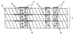
図1は、本発明の配線基板の実施の形態の一例における構成例を示す断面図である。図1に示されるように、本例の配線基板1は、セラミックスからなる絶縁基板2と、絶縁基板2に設けられた複数のビア導体3とを備える。このビア導体3は、絶縁基板1を構成する絶縁層に設けられた貫通孔に導体が充填されて形成されている貫通導体である。また、配線基板1の表面および内部には、広面積のいわゆるベタパターンや、配線導体である線状のラインパターンよりなる、回路4を備える。複数のビア導体3は、径が異なる複数のビア導体からなり、各ビア導体3は絶縁成分5をそれぞれ含む。また、回路4は、絶縁基板2の内部および表面に設けられ、ビア導体3と同様に絶縁成分5を含んでいる。ここで、絶縁成分5は、絶縁基板2に含まれるセラミックスと同じくセラミックスからなるものである。
FIG. 1 is a cross-sectional view showing a configuration example in an example of an embodiment of a wiring board of the present invention. As shown in FIG. 1, the
例えば、セラミックスからなる絶縁基板2は、酸化アルミニウム質焼結体,窒化アルミニウム質焼結体,ムライト質焼結体,炭化珪素質焼結体、窒化珪素質焼結体、またはガラスセラミックス焼結体等のセラミック材料により形成される。そして、ビア導体3が有するセラミックスからなる絶縁成分5も、これらセラミック材料により形成される。
For example, the
ここで、本例の配線基板1では、径の大きいビア導体3ほど、全体に対する絶縁成分5の質量比が大きくなっている。このように、ビア導体3における絶縁成分5の質量比を、ビア導体3の径が大きくなるに従って大きくなっているものとすると、ビア導体3の径に関わらず絶縁成分5の質量比を同じにした場合と比べて、径の小さいビア導体3の抵抗値が大きくなり過ぎることを抑制して所望の抵抗値を満足することができ、一方で径の大きいビア導体3の収縮挙動を調整して周辺の絶縁基板2にクラックが発生することを抑制することができる。
Here, in the
ビア導体3における絶縁成分5の質量比は、例えば、ビア導体3の径が30μmと小さい場合は絶縁成分5の添加量(質量比)は5乃至10質量%とし、それに対してビア導体3の径が150μmと大きい場合は絶縁成分5の添加量(質量比)は15乃至30質量%と大きくすると、径の小さいビア導体3では抵抗値を低く維持して満足させることができ、かつ径の大きいビア導体3では周辺の絶縁基板2にクラックが発生することを十分に抑制することができるものとなる。
The mass ratio of the
また、絶縁成分5はビア導体3において粒子状の形態で存在しているものであるが、ビア導体3における絶縁成分5の大きさは、ビア導体3の径が大きくなるに従って大きくする方が、抵抗値の上昇の抑制を考慮した少ない絶縁成分5の添加量(質量比)でもクラックが発生しにくくなり、絶縁成分5を効果的に機能させることができるので好ましい。例えば、ビア導体3の径が30μm程度と小さい場合であれば、絶縁成分5の大きさは10μm以下の程度とすればよく、これに対してビア導体の径が100μm程度と大きい場合であれば、絶縁成分5の大きさは大きくして30μm以下の程度とすれば、比較的少ない絶縁成分5の添加量(比較的小さい質量比)でも径の大きいビア導体3の周辺において絶縁基板2にクラックが発生しにくくなり、径の小さいビア導体3における絶縁成分5と同じ大きさの絶縁成分5を用いる場合よりも効果的であるので好ましい。
Further, the
ビア導体3における絶縁成分5の大きさは、ビア導体3の作製時に添加した絶縁成分5の大きさによって制御することができる。また、作製後においては、例えば絶縁成分5の体積を、ビア導体3を透過X線により投影した画像から絶縁成分5の領域を検出して測定し、あるいはビア導体3のX線断層写真から絶縁成分5の部分を検出して測定し、その測定した体積と同じ体積を持つ球の直径を絶縁成分5の粒子の大きさとして確認することができる。
The size of the
また、本例の配線基板1では、絶縁成分5は、軟化点がビア導体3の導体成分のTMA法(Thermomechanical Analysis:熱機械分析)によって求めた収縮開始温度よりも低いガラス成分と、TMA法によって求めた収縮開始温度が絶縁基板2の焼成温度よりも高いセラミック成分とからなり、絶縁成分5中のガラス成分の比率は、ビア導体3の径が大きくなるに従って大きくなっていることが好ましい。
In the
これは、絶縁成分5を、ビア導体3を構成する導体成分のTMA法によって求めた収縮開始温度よりも軟化点が低いガラス成分と、絶縁基板2の焼成温度よりもTMA法によって求めた収縮開始温度が高いセラミック成分とからなるものとすることで、特に径の大きいビア導体3において、比較的少ない絶縁成分5の添加量(比較的小さい質量比)でも、配線基板1の焼成時におけるビア導体3の焼結挙動の調整がより容易となるため、絶縁成分5の質量比を必要以上に大きくしなくともよくなって抑えることができるからである。また、ビア導体3の径が大きくなると、焼成中に絶縁基板2からビア導体3に拡散してくるガラス成分がビア導体3の中心部には拡散しにくくなり、焼結後にビア導体3の中心部にガラス成分が不足した空孔が発生しやすくなるのに対して、ビア導体3の径が大きくなるのに応じてガラス成分の比率を大きくすることで、ビア導体3の中心部にもガラス成分が存在するようになることから、ビア導体3の中心部の空孔を発生しにくくさせることができ、抵抗値を良好に維持する上でも、収縮挙動を調整する上でも好ましいものとなる。
This is because the
ここで、ビア導体3の導体成分および絶縁成分5のセラミック成分についてのTMA法によって求めた収縮開始温度とは、JIS R3102「ガラスの平均線膨張係数の試験方法」に準じて測定して求めたものであり、ビア導体3の導体成分からなる試料粉末および絶縁成分5のセラミック成分からなる試料粉末をそれぞれ250メッシュの篩に通して、得られた粉を成形金型に入れ、3乃至10MPa程度の圧力で常温にて5乃至30秒程度プレスすることによって、直径6mmおよび高さ10mmの円柱状のバルクを成形し、このバルクを用いて、空気または窒素等の雰囲気中で10℃/分の昇温速度で焼成しながら、そのときの高さ方向の寸法の変化を熱機械分析(TMA)法で測定して、それによって求められた、バルクが収縮を開始する温度である。
Here, the shrinkage initiation temperature obtained by the TMA method for the conductor component of the via
絶縁成分5中のガラス成分の比率は、例えば、ビア導体3の径が30μmと小さい場合での絶縁成分5の添加量(質量比)が5質量%であり、ビア導体3の径が150μmと大きい場合での絶縁成分5の添加量(質量比)が30質量%であるとすると、ビア導体3の径が30μmの場合の絶縁成分5中のガラス成分の比率を10乃至30質量%とし、ビア導体3の径が150μmの場合の絶縁成分5中のガラス成分の比率を30乃至80質量%とすると、絶縁成分5の添加量がそれぞれ3乃至8質量%および10乃至20質量%であれば、ビア導体3の周辺における絶縁基板2のクラックの発生を抑制し、かつ径が150μmと大きいビア導体3での中心部の空孔の発生を抑制することができる。
The ratio of the glass component in the insulating
絶縁成分5中のガラス成分としては、例えばSiO2−B2O3系、SiO2−B2O3−Al2O3系,SiO2−B2O3−Al2O3−MO系(ただし、MはCa,Sr,Mg,BaまたはZnを示す),SiO2−Al2O3−M1O−M2O系(ただし、M1およびM2は同じまたは異なってCa,Sr,Mg,BaまたはZnを示す),SiO2−B2O3−Al2O3−M1O−M2O系(ただし、M1およびM2は上記と同じである),SiO2−B2O3−M32O系(ただし、M3はLi、NaまたはKを示す),もしくはSiO2−B2O3−Al2O3−M32O系(ただし、M3は上記と同じである),Pb系ガラス,Bi系ガラス等が挙げられる。
Examples of the glass component in the insulating
なお、ガラス成分の軟化点は、ビア導体3の導体成分のTMA法によって求めた収縮開始温度よりも10乃至100℃度程度低いことが好ましい。この範囲であれば、ガラス成分によるビア導体3の効果的な収縮調整が可能となり、好ましい。例えば、ビア導体3の導体成分のTMA法によって求めた収縮開始温度が800℃程度の銅であれば、絶縁成分5のガラス成分として軟化点が700乃至790℃程度のものを用いることにより、ガラス成分によるビア導体3の効果的な収縮調整が可能となる。
The softening point of the glass component is preferably about 10 to 100 ° C. lower than the shrinkage start temperature obtained by the TMA method of the conductor component of the via
また、絶縁成分5のセラミック成分としては、絶縁基板2を構成するセラミックスと同様のものを用いることができ、例えば、Al2O3,SiO2,ZrO2とアルカリ土類金属酸化物との複合酸化物,TiO2とアルカリ土類金属酸化物との複合酸化物,ならびにAl2O3およびSiO2から選ばれる少なくとも1種を含む複合酸化物(例えばスピネル,ムライト,コージェライト)等が挙げられる。
Further, as the ceramic component of the insulating
絶縁成分5のセラミック成分のTMA法によって求めた収縮開始温度は、絶縁基板2の焼成温度より100℃以上高いことが好ましい。この範囲であれば、セラミック成分によるビア導体3の効果的な収縮調整が可能となり、好ましい。例えば、絶縁基板2の焼成温度が1000℃程度であれば、TMA法によって求めた収縮開始温度が1100℃以上のアルミナ,シリカまたは二酸化チタン等を絶縁成分5のセラミック成分に用いることにより、セラミック成分によるビア導体3の効果的な収縮調整が可能となる。
The shrinkage start temperature obtained by the TMA method of the ceramic component of the insulating
また、ビア導体3や回路4の導体材料としては、例えばタングステン(W),モリブデン(Mo),マンガン(Mn),金(Au),銀(Ag),銅(Cu),パラジウム(Pd)および白金(Pt)のうち1種または2種以上が挙げられ、絶縁基板2の材料等により使い分けることが可能である。ここで、銅,銀もしくは金を用いると、ビア導体3および回路4の抵抗値が低くなるため、高周波の信号が通りやすくなることから、好ましい。
Examples of the conductor material for the via
また、回路4における、広面積のいわゆるベタパターンや、配線導体である線状のラインパターンについても絶縁成分5と同様の絶縁成分を有するものとするときには、その質量比は、広面積のパターンであるベタパターンにおける絶縁成分5の質量比を線状のパターンであるラインパターンにおける質量比よりも高くすることにより、ビア導体3における場合と同様に、ベタパターンの周辺における絶縁基板2のクラックの発生を抑制し、かつラインパターンの抵抗値を低く維持することができるので、好ましい。例えば、幅が50μm程度のラインパターンでは絶縁成分の質量比は1乃至8質量%程度とし、ベタパターンでは絶縁成分の質量比は5乃至15質量%程度とすることで、ベタパターンの周辺における絶縁基板2のクラックの発生を抑制し、かつラインパターンの抵抗値を低く維持することができる。
In addition, when the
次に、本発明の配線基板の製造方法の実施の形態の例について、配線基板1を例にとって図2を参照しつつ説明する。図2(a)および(b)は、配線基板1の製造方法の一例をそれぞれ工程順に示した断面図であり、図2において図1に示す配線基板1に対応する部位には同じ符号を括弧を付して示してある。
Next, an example of an embodiment of a method for manufacturing a wiring board according to the present invention will be described with reference to FIG. 2 taking the
まず、図2(a)に示すように、絶縁基板2となるセラミックグリーンシート6に複数の大きさの径を持つ、ビア導体3を形成するための貫通孔であるビア孔7を複数形成する。セラミックグリーンシート6は、例えば酸化アルミニウム,酸化珪素および酸化カルシウム等の原料粉末を、バインダ樹脂および溶剤とともに混練してスラリーを得て、このスラリーをドクターブレード法もしくはリップコータ法等によってキャリア上にシート状に成形して形成される。ここでセラミックグリーンシート6にビア孔7を形成する方法としては、ビア孔7と同じ径を持つピンを打ち込む方法や、CO2レーザやUV−YAGレーザ等のレーザ光を照射する方法等を採用することができる。ここで、ビア孔7を形成する方法としてレーザ光を照射する方法を用いると、ピンを打ち込む方法のように複数の大きさの径のピンを準備する必要がなく、複数の径のビア孔7を一度に形成でき、かつセラミックグリーンシート6をキャリア付きのままでビア孔7形成に使用できることから、工程中や保管中等のセラミックグリーンシート6の寸法変動を抑えることができるので、好ましい。
First, as shown in FIG. 2A, a plurality of via
次に、図2(b)に示すように、ビア孔7へビア導体3となる導体ペーストを充填し、それに接続するようにセラミックグリーンシート6の表面に回路4となる導体ペーストを塗布する。この場合に、ビア孔7へ導体ペーストを充填する工程と、セラミックグリーンシート6の表面に導体ペーストを塗布する工程とは、どちらが先でもよい。また、ビア孔7へ導体ペーストを充填する方法およびセラミックグリーンシート6の表面に導体ペーストを塗布する方法としては、印刷用のマスクの開口部から導体ペーストを塗布するスクリーン印刷法およびインクジェットやディスペンサー等の導体ペーストを直接描画する方法等のいずれの方法も適用することができる。
Next, as shown in FIG. 2 (b), the via
このような導体ペーストは、導体成分となる導体粒子8および絶縁成分5となる絶縁粒子9にバインダ樹脂および溶剤を調合して、加熱および混合することにより作製される。
Such a conductor paste is prepared by preparing a binder resin and a solvent in the
導体粒子8は、例えばタングステン(W),モリブデン(Mo),マンガン(Mn),金(Au),銀(Ag),銅(Cu),パラジウム(Pd)または白金(Pt)等の金属粉末をアトマイズ法または還元法等により処理して製造されたものであり、必要により酸化防止または凝集防止等の処理を行なってもよい。導体粒子8が2種類以上の場合は、2種類以上の粉末を混合してもよいし、合金またはコーティング等により2種類以上の金属材料が一体となった粉末を用いてもよい。また、分級等により微粉末または粗粉末を除去して粒度分布を所望の分布に調整したものであってもよい。
The
また、絶縁成分5となる絶縁粒子9は、SiO2−B2O3系,SiO2−B2O3−Al2O3系,SiO2−B2O3−Al2O3−MO系(ただし、MはCa,Sr,Mg,BaまたはZnを示す),SiO2−Al2O3−M1O−M2O系(ただし、M1およびM2は同じまたは異なってCa,Sr,Mg,BaまたはZnを示す),SiO2−B2O3−Al2O3−M1O−M2O系(ただし、M1およびM2は上記と同じである),SiO2−B2O3−M32O系(ただし、M3はLi、NaまたはKを示す),もしくはSiO2−B2O3−Al2O3−M32O系(ただし、M3は上記と同じである),Pb系ガラス,Bi系ガラス等のガラス粉末や、Al2O3,SiO2,ZrO2とアルカリ土類金属酸化物との複合酸化物,TiO2とアルカリ土類金属酸化物との複合酸化物,ならびにAl2O3およびSiO2から選ばれる少なくとも1種を含む複合酸化物(例えばスピネル,ムライト,コージェライト)等のセラミック粉末を、アトマイズ法により製造したものや、ボールミル等で粉砕処理したもの等を用いることができる。また、必要により酸化防止または凝集防止等の処理を行なってもよい。絶縁粒子9が2種類以上の場合は、2種類以上の粉末を混合してもよいし、コーティング等により2種類以上の絶縁材料が一体となった粉末を用いてもよい。また、分級等により微粉末または粗粉末を除去して粒度分布を所望の分布に調整したものであってもよい。
Insulating
ここで、ビア導体3における絶縁成分5の質量比を、ビア導体3の径が大きくなるに従って大きくなるように調整するために、また必要に応じて回路4におけるベタパターンとラインパターンとで絶縁成分の質量比を変えるために、導体ペーストに含まれる絶縁粒子9の添加量(質量比)を調整したものをビア孔7(ビア導体3)の径の大きさに応じて複数作製し、ビア孔7の径の大きさに応じて、ならびに必要に応じて回路4のベタパターンおよびラインパターンに応じて各々の導体ペーストを用いて、ビア孔7への導体ペーストの充填および回路4となる導体パターンの塗布を複数回行なう。これにより、径が大きくなるに従って絶縁成分5の質量比が大きくなっているビア導体3を、パターンに応じて絶縁成分の質量比を変えた回路4とともに形成することができる。
Here, in order to adjust the mass ratio of the insulating
導体ペーストに含まれるバインダ樹脂は、従来から導体ペーストに使用されているものが使用可能である。例えば、アクリル系(アクリル酸,メタクリル酸またはそれらのエステルの単独重合体または共重合体,具体的にはアクリル酸エステル共重合体,メタクリル酸エステル共重合体,アクリル酸エステル−メタクリル酸エステル共重合体等),ポリビニルブチラール系,ポリビニルアルコール系,アクリル−スチレン系,ポリプロピレンカーボネート系,セルロース系等の単独重合体または共重合体が挙げられる。樹脂の選定に当たっては、焼成工程での分解および揮発性を考慮すると、アクリル系またはアルキド系の有機バインダが好ましい。また、樹脂の添加量としては、導体ペーストに用いる導体粒子8および絶縁粒子9の種類等により異なるが、焼成時に分解・除去されやすく、かつ導体粒子8および絶縁粒子9を良好に分散できる量であればよく、その目安としては導体粒子8に対して5乃至20質量%程度が望ましい。また、溶剤としては、テルピネオール,ブチルカルビトールアセテートおよびフタル酸等の可塑剤等が使用可能である。
As the binder resin contained in the conductor paste, those conventionally used in the conductor paste can be used. For example, acrylic (a homopolymer or copolymer of acrylic acid, methacrylic acid or esters thereof, specifically acrylic ester copolymer, methacrylic ester copolymer, acrylic ester-methacrylic ester copolymer Homopolymers or copolymers of polyvinyl butyral, polyvinyl alcohol, acrylic-styrene, polypropylene carbonate, cellulose, etc. In selecting the resin, an acrylic or alkyd organic binder is preferable in consideration of decomposition and volatility in the firing step. The amount of resin added varies depending on the type of
ここで、ビア孔7を充填するための導体ペーストに、導体ペースト中の溶剤成分がセラミックグリーンシート6へ浸透するのを抑制する浸透抑制剤を添加すると、導体ペーストの充填の際に、導体ペーストからセラミックグリーンシート6に導体ペーストに含まれる溶剤がセラミックグリーンシート6に吸収されにくくなるため、充填中に導体ペーストの粘度が上昇しにくくなり、安定した充填が行なえるようになる。このように、導体ペーストをセラミックグリーンシート6への溶剤成分の浸透を抑制する浸透抑制剤を有するものとすると、特にビア孔7の径が小さい場合に、および導体ペーストの粘度が高い場合においても、導体ペーストをビア孔7に良好に充填しやすくなる。その結果、ビア導体3の周辺部やビア導体3の内部において、導体ペーストの乾燥収縮に伴うクラックが発生しにくくなる。
Here, when a penetration inhibitor that suppresses penetration of the solvent component in the conductor paste into the ceramic
この浸透抑制剤の添加量は、ビア孔7の径の大きさにより調整するとよい。具体的には、ビア孔7の径が大きいものほど浸透抑制剤の添加量を少なくするとよい。このようにすると、径の大きいビア孔7において、導体ペーストの埋め込み時にセラミックグリーンシート6の裏表面への導体ペーストの滲み等が発生しにくくなり、かつ径の小さいビア孔7においてもビア孔7への充填性が向上することから、ビア導体3の周辺部や周辺の絶縁基板2に、またビア導体3の内部にクラックが発生しにくくなる。この場合には、複数の添加量を変更した導体ペーストを準備し、ビア孔7の径の大きさに応じて使い分けて充填することによって、良好な充填を行なうことができる。
The amount of the penetration inhibitor added may be adjusted according to the diameter of the via
このような浸透抑制剤の添加量としては、例えば、ビア孔7の径が40μmと小さいときはバインダ樹脂および溶剤の総量に対して10乃至20質量%の範囲であれば、一方、ビア孔7の径の大きさが100μmと大きいときは0.1乃至5質量%の範囲であれば、ビア孔7の径の大きさが40μm程度と小さいときにおいては充填性を向上させることができ、一方、ビア孔7の径の大きさが100μm程度と大きいときにおいては導体ペーストの滲みの発生が低減できるので、好ましい。
For example, when the diameter of the via
また、浸透抑制剤は、ひまし油を含むことが好ましい。浸透抑制剤がひまし油を含むこにより、ひまし油に含まれる網目構造に溶剤が保持されるため、導体ペーストから溶剤がセラミックグリーンシート6に浸透したり揮発したりするのを効果的に抑制することができる。また、ひまし油による網目構造の保持力を調整することにより、導体ペーストの充填時に網目構造から溶剤が放出されるようにすることもできるため、その場合には導体ペーストの粘度を低下させることができ、ビア孔7に導体ペーストを充填しやすくなる。よって、ビア導体3の周辺部やビア導体3の内部において、導体ペーストの乾燥収縮に伴うクラックの発生を抑制することができる。ここで用いるひまし油には、水素を添加したもの等が適用できる。水素添加ひまし油は、導体ペーストに含まれる溶剤と水素結合することで溶剤の保持力をより強固にすることができることから、より少ない浸透抑制剤の添加量でも導体ペーストを良好に充填できるようになるので、好ましい。
Moreover, it is preferable that a penetration inhibitor contains castor oil. Since the penetration inhibitor contains castor oil, the solvent is retained in the network structure contained in the castor oil, so that the solvent can effectively prevent the solvent from penetrating into the ceramic
また、導体ペーストの製造において、浸透抑制剤とバインダ樹脂と溶剤とをあらかじめ加熱および混合しておき、その後に導体粒子8および絶縁粒子9と加熱および混合する方法によれば、導体粒子8および絶縁粒子9の表面に浸透抑制剤が付着して固化したりせず、バインダ樹脂および溶剤中(以下、樹脂等ともいう)に浸透抑制剤が分散しやすくなることから、より少ない浸透抑制剤の添加量でも、導体ペーストの充填時において、導体ペーストに含まれる溶剤がセラミックグリーンシート6に浸透しにくくなり吸収されにくくなる。このとき、浸透抑制剤と樹脂等とをあらかじめ加熱する際の温度は、導体ペーストを作製する際に加熱する温度よりも高い方が好ましい。これは、そのようにすると、経時変化による浸透抑制剤と樹脂等との分離が無く、分散後の状態がより安定しやすくなるからである。浸透抑制剤と樹脂等とをあらかじめ加熱する際の温度は、樹脂等および浸透抑制剤の種類により異なるが、バインダ樹脂としてアクリル樹脂を、溶剤としてテルピネオールをそれぞれ用いる場合は、30乃至80℃の範囲であれば、分散後に放置しておいても導体ペーストが樹脂等と浸透抑制剤とに分離することを抑制することができ、より少ない浸透抑制剤の添加量でも、ビア孔7への導体ペーストの充填時において導体ペーストに含まれる溶剤がセラミックグリーンシート6に吸収されにくくなる。
Further, in the production of the conductor paste, according to the method in which the permeation inhibitor, the binder resin, and the solvent are heated and mixed in advance and then heated and mixed with the
また、ビア導体3を形成するためのビア孔7に充填される導体ペーストと、回路4を形成するためのセラミックグリーンシート6の表面に塗布される導体ペーストとは、同じものを使用してもよいが、ビア孔7に充填される導体ペーストに含まれる導体粒子8の粒度分布を、回路4を形成する導体ペーストに含まれる導体粒子8の粒度分布よりも広くすると、焼成の際の収縮挙動の調整がより容易となり、ビア導体3の周辺の絶縁基板2にクラックが発生しにくくなる。
Also, the same conductor paste may be used as the conductor paste filled in the via
また、PETフィルム等のキャリア上に載置されたセラミックグリーンシート6にレーザ光を照射することによりビア孔7を形成し、そのビア孔7に導体ペーストの充填を行ない、充填後にセラミックグリーンシート6からキャリアを剥離すると、セラミックグリーンシート6の表面への導体ペーストの滲みがなくなることから、高密度にビア孔7を形成しても、それに充填した導体ペーストの滲みによるビア導体3間の短絡が発生しにくくなる。
Also, via
最後に、図2(c)に示すように、ビア孔7に導体ペーストが充填され、表面に回路4となる導体ペーストが塗布されたセラミックグリーンシート6を複数枚積層し、この積層体の焼成を行なうことにより、配線基板1が完成する。なお、焼成後に、配線基板1の断面を研磨する等の破壊検査またはX線等による透過光を用いた非破壊検査等によって、ビア導体3に含まれる絶縁成分5および回路4に含まれる絶縁成分の状態を確認することができる。
Finally, as shown in FIG. 2 (c), a plurality of ceramic
絶縁成分5の粒径の大きさの算出方法としては、例えば、ビア導体3の断面を研磨して絶縁成分5の最大長および絶縁成分5の面積を測定し、その面積と同じ面積を持つ円の直径を絶縁成分5の粒径の大きさとする方法、またはビア導体3を透過X線により投影した画像から絶縁成分5の領域を検出して、あるいはビア導体3のX線断層写真から絶縁成分5の部分を検出して絶縁成分5の体積を測定し、その測定した体積と同じ体積を持つ球の直径を絶縁成分5の粒径の大きさとする方法がある。同様に、ビア導体3における絶縁成分5の質量比についても、ビア導体3の面積に占める絶縁成分5の面積、またはビア導体3の体積に占める絶縁成分5の体積を測定することにより、ビア導体3における絶縁成分5の質量比を算出することができる。
As a method of calculating the size of the particle size of the insulating
ここで、絶縁基板2としてガラスセラミックスのような低温焼結材料を用いる場合は、複数枚のセラミックグリーンシート6を積層した積層体の上下面にさらに拘束グリーンシートを積層して焼成し、焼成後に拘束シートを除去するようにすれば、より高寸法精度の配線基板1を得ることが可能となるので、好ましい。なお、この拘束グリーンシートは、Al2O3等の難焼結性無機材料を主成分とするグリーンシートであり、絶縁基板2の焼成時に収縮しないものである。この拘束グリーンシートが積層された積層体は、収縮しない拘束グリーンシートにより積層平面方向(x−y平面方向)の収縮が抑制され、主に積層方向(z方向)に収縮するので、焼成収縮に伴う絶縁基板2の寸法ばらつきが抑制される。
Here, when a low-temperature sintered material such as glass ceramics is used as the insulating
ここで、配線基板1の表面に形成される回路4に絶縁成分が含まれていれば、回路4に含まれる絶縁成分と拘束グリーンシートとの反応によって両者の接合強度が増し、より収縮しにくくなるので好ましいが、絶縁成分の比率が大きい場合は、特に回路4の接触面積が小さい場合には回路4と拘束グリーンシートとの接合強度が強くなり、焼成後に拘束グリーンシートが完全に除去できなかったり、あるいは回路4が絶縁基板2から剥がれたりすることがある。また逆に、絶縁成分の比率が小さい場合は、特に回路4の接触面積が大きい場合には回路4と拘束グリーンシートとの接合強度が弱くなり、絶縁基板2の寸法ばらつきが発生することがある。この場合には、前述のように回路4の面積の大きさに応じて含有させる絶縁成分の質量比を変化させると、回路4との接触面積に関わらず拘束グリーンシートを容易に除去することができ、かつ回路4と拘束グリーンシートとの接合強度が適度になり、絶縁基板2の寸法ばらつきが抑制されることから、好ましい。
Here, if the
また、この拘束グリーンシートには、難焼結性無機成分に加えて、絶縁基板2の焼成温度以下の軟化点を有するガラス成分、例えばセラミックグリーンシート6中のガラス成分と同じガラス成分を含有させるとよい。そうすると、焼成中にこのガラス成分が軟化してセラミックグリーンシート6と結合することにより、セラミックグリーンシート6と拘束グリーンシートとの結合が強固となり、より確実な拘束力が得られる。このときのガラス成分の含有量は、難焼結性無機成分とガラス成分とを合わせた無機成分の量に対して外添加で0.5乃至15質量%とするとよく、これによって、拘束力が向上し、かつ拘束グリーンシートの焼成収縮が0.5%以下に抑えられる。
In addition to the hardly sinterable inorganic component, the constrained green sheet contains a glass component having a softening point equal to or lower than the firing temperature of the insulating
またこの場合は、回路4に含まれる絶縁成分と拘束グリーンシートに含まれるガラス成分とが反応することから、回路4に含まれる絶縁成分の質量比をより少なくしても、拘束グリーンシートとの接合強度を適度に確保することができるとともに、絶縁基板2の寸法ばらつきを抑制できるので、好ましい。
In this case, since the insulating component included in the
焼成後の配線基板1からの拘束シートの除去方法としては、例えば研磨,ウォータージェット,ケミカルブラスト,サンドブラストまたはウェットブラスト(砥粒と水とを空気圧により噴射させる方法)等が挙げられる。
Examples of a method for removing the constraining sheet from the
なお、ビア導体3には、絶縁基板2を構成する各絶縁層を貫通するものだけではなく、絶縁基板2の全体を貫通するものも含まれる。
The via
焼成後の配線基板1の表面に形成された回路4の表面には、腐食防止のために、または半田や金属ワイヤ等の、外部の配線基板や実装される電子部品との接続手段との良好な接続のために、ニッケル(Ni)や金(Au)のめっきを施すとよい。
The surface of the
なお、本発明は上述の実施の形態の例に限定されるものではなく、本発明の要旨の範囲内であれば、種々の変形は可能である。 In addition, this invention is not limited to the example of above-mentioned embodiment, A various deformation | transformation is possible if it is in the range of the summary of this invention.
[第1の実施例]
本発明の配線基板の第1の実施例について以下に説明する。
[First embodiment]
A first embodiment of the wiring board of the present invention will be described below.
まず、Al2O3からなるセラミック粉末およびSiO2−B2O3−Al2O3からなるガラス粉末を混合したものを100質量部として、アクリル系のバインダ樹脂を10質量部、および可塑剤を1質量部添加し、トルエンおよび酢酸エチルを溶剤としてボールミルにより40時間混合し、スラリーを調製した。このスラリーからダイコーターシート成形機を用いて、成形速度が2m/分で成形シート幅が250mmの条件にてポリエチレンテレフタレート(PET)のシートからなる支持体上に塗布して、厚みが50μmのセラミックグリーンシートを形成した。
First, 100 parts by weight of a mixture of ceramic powder made of Al 2 O 3 and glass powder made of SiO 2 —B 2 O 3 —Al 2 O 3 , 10 parts by weight of an acrylic binder resin, and
次に、導体粒子としてのCu粉末に対して、SiO2−B2O3−Al2O3からなる軟化点が600℃のガラス粉末とSiO2粉末とを1:1で混合したものを絶縁粒子として、1,3,5,10,15,20,25および30質量%の添加量(絶縁成分の質量比に相当)で添加し、アクリル系のバインダ樹脂およびテルピネオール(TPO)からなる溶剤と混合して、導体ペーストを作製した。 Next, a mixture of glass powder having a softening point of 600 ° C. made of SiO 2 —B 2 O 3 —Al 2 O 3 and SiO 2 powder in a 1: 1 ratio with respect to Cu powder as conductor particles is insulated. As a particle, added in an amount of 1,3,5,10,15,20,25 and 30% by mass (corresponding to the mass ratio of insulating components), and a solvent comprising an acrylic binder resin and terpineol (TPO) A conductor paste was prepared by mixing.
次に、レーザ光を発生するレーザ装置としてCO2レーザ装置を用い、セラミックグリーンシートに径の大きさが30μmおよび150μmのビア孔としての貫通孔を200μm間隔で縦横20列の計各400個形成した。形成した貫通孔には、支持体側から導体ペーストを充填して埋め込んだ。この導体ペーストを埋め込んだセラミックグリーンシートを4枚重ね合わせて厚み方向に5MPaの圧力および80℃の温度で加熱圧着して、セラミックグリーンシート積層体を作製した。それから、得られたセラミックグリーンシート積層体中のバインダ樹脂および溶剤等の有機成分や、有機成分が分解した後に残留するカーボンを除去するため、7.33kPaの分圧の水蒸気を含んだ窒素雰囲気中に約700℃の温度で1時間保持する熱処理を行なった後、還元雰囲気中にて約1000℃の温度で1時間保持して、ビア導体における絶縁成分の質量比が異なる、評価用の実施例1〜9の配線基板を作製した。 Next, a CO 2 laser device is used as a laser device that generates laser light, and a total of 400 through-holes are formed on the ceramic green sheet as via holes with diameters of 30 μm and 150 μm in 20 rows vertically and horizontally at intervals of 200 μm. did. The formed through-hole was filled with a conductive paste from the support side. Four ceramic green sheets embedded with this conductive paste were stacked and heat-pressed at a pressure of 5 MPa and a temperature of 80 ° C. in the thickness direction to produce a ceramic green sheet laminate. Then, in order to remove organic components such as binder resin and solvent in the obtained ceramic green sheet laminate and carbon remaining after decomposition of the organic components, in a nitrogen atmosphere containing water vapor with a partial pressure of 7.33 kPa Example 1 for evaluation in which heat treatment is performed at a temperature of about 700 ° C. for 1 hour, and then held in a reducing atmosphere at a temperature of about 1000 ° C. for 1 hour, so that the mass ratio of insulating components in the via conductor is different. -9 wiring boards were produced.
そして、これら実施例1〜9の配線基板について、双眼顕微鏡によりビア導体近傍のクラック発生の有無を観察し、ビア導体の表裏面に抵抗測定器の電極端子を当ててビア導体の抵抗値を測定した。 And about the wiring board of these Examples 1-9, the presence or absence of the crack generation | occurrence | production of a via conductor vicinity is observed with a binocular microscope, the electrode terminal of a resistance measuring device is applied to the front and back of a via conductor, and the resistance value of a via conductor is measured. did.
これら実施例1〜9について、導体ペーストに添加した絶縁粒子の添加量(絶縁成分の質量比)と、ビア導体の径別のクラックおよび抵抗値の評価の結果とを表1に示す。 Table 1 shows the amount of insulating particles added to the conductor paste (mass ratio of insulating components) and the results of evaluation of cracks and resistance values according to the diameter of the via conductors for Examples 1 to 9.

表1に示す結果において、「クラック」欄の「○」は、ビア導体近傍のクラックの発生が見られず、優れていたことを示す。一方、「△」は、一部のビア導体近傍に実用上は支障がない程度ではあるがわずかにクラックの発生が確認されたことを示す。また、「抵抗値」欄の「○」は、抵抗要求値を十分に満足し、優れていたことを示す。一方、「△」は、一部のビア導体の抵抗値が要求値の上限程度でやや高かったものを示す。 In the results shown in Table 1, “◯” in the “crack” column indicates that the generation of cracks in the vicinity of the via conductor was not observed and was excellent. On the other hand, “Δ” indicates that the occurrence of a slight crack was confirmed in the vicinity of some via conductors, although there was no practical problem. In addition, “◯” in the “resistance value” column indicates that the required resistance value is sufficiently satisfied and is excellent. On the other hand, “Δ” indicates that the resistance value of some via conductors is slightly high at the upper limit of the required value.
表1に示す結果から明らかなように、ビア導体の径が30μmの場合では、導体ペーストに添加するセラミック粉末の添加量(ビア導体における絶縁成分の質量比)が5質量%未満の実施例1,2では、ビア導体近傍にわずかにクラックが発生した(表中の「クラック」の欄に「△」で示す)。また、導体ペーストに添加したセラミック粉末の添加量(ビア導体における絶縁成分の質量比)が10質量%より多い実施例5,6,7,8,9では、抵抗値が抵抗要求値の上限程度でやや高い値を示した(表中の「抵抗値」の欄に「△」で示す)。これに対して、導体ペーストに添加するセラミック粉末の添加量(ビア導体における絶縁成分の質量比)が5乃至10質量%の実施例3,4では、ビア導体近傍にクラックの発生が無く、抵抗要求値も十分に満足する優れたものであった(表中の「総合判定」の欄に「○」で示す)。 As is apparent from the results shown in Table 1, when the diameter of the via conductor is 30 μm, Example 1 in which the amount of ceramic powder added to the conductor paste (mass ratio of insulating components in the via conductor) is less than 5 mass% , 2, a slight crack occurred in the vicinity of the via conductor (indicated by “Δ” in the “crack” column in the table). In Examples 5, 6, 7, 8, and 9 in which the amount of ceramic powder added to the conductor paste (mass ratio of insulating components in the via conductor) is more than 10 mass%, the resistance value is about the upper limit of the required resistance value. A slightly high value was indicated (indicated by “Δ” in the “resistance value” column in the table). On the other hand, in Examples 3 and 4 in which the amount of ceramic powder added to the conductor paste (mass ratio of insulating components in the via conductor) is 5 to 10% by mass, there is no crack in the vicinity of the via conductor, and resistance The required value was also excellent enough to be satisfied (indicated by “◯” in the “Comprehensive judgment” column in the table).
また、ビア導体の径が150μmの場合では、導体ペーストに添加したセラミック粉末の添加量(ビア導体における絶縁成分の質量比)が15質量%未満の実施例1,2,3,4では、ビア導体近傍にわずかにクラックが発生した(表中の「クラック」の欄に「△」で示す)。また、導体ペーストに添加するセラミック粉末の添加量(ビア導体における絶縁成分の質量比)が30質量%より多い実施例9では、抵抗値が抵抗要求値の上限程度でやや高い値を示した(表中の「抵抗値」の欄に「△」で示す)。 Further, when the diameter of the via conductor is 150 μm, in Examples 1, 2, 3, and 4 in which the amount of ceramic powder added to the conductor paste (mass ratio of insulating components in the via conductor) is less than 15% by mass, A slight crack occurred in the vicinity of the conductor (indicated by “Δ” in the “crack” column in the table). Further, in Example 9 in which the amount of ceramic powder added to the conductor paste (mass ratio of insulating components in the via conductor) is more than 30% by mass, the resistance value was slightly higher than the upper limit of the required resistance value ( ("△" is shown in the "resistance value" column in the table).
これに対して、導体ペーストに添加するセラミック粉末の添加量(ビア導体における絶縁成分の質量比)が15乃至30質量%の実施例5,6,7,8では、ビア導体近傍にクラックの発生が無く、抵抗要求値も十分に満足する優れたものであった(表中の「総合判定」の欄に「○」で示す)。 On the other hand, in Examples 5, 6, 7, and 8 in which the amount of ceramic powder added to the conductor paste (mass ratio of insulating components in the via conductor) is 15 to 30% by mass, cracks are generated in the vicinity of the via conductor. And the resistance requirement value was also excellent enough (indicated by “◯” in the column of “Comprehensive judgment” in the table).
[第2の実施例]
本発明の配線基板の第2の実施例について以下に説明する。
[Second Embodiment]
A second embodiment of the wiring board of the present invention will be described below.
まず、Al2O3から成るセラミック粉末およびSiO2−B2O3−Al2O3からなるガラス粉末を混合したものを100質量部として、アクリル系のバインダ樹脂を10質量部、および可塑剤を1質量部添加し、トルエンおよび酢酸エチルを溶剤としてボールミルにより40時間混合し、スラリーを調製した。このスラリーからダイコーターシート成形機を用いて、成形速度が2m/分で成形シート幅が250mmの条件にてポリエチレンテレフタレート(PET)のシートからなる支持体上に塗布して、厚みが50μmのセラミックグリーンシートを形成した。
First, 100 parts by mass of ceramic powder composed of Al 2 O 3 and glass powder composed of SiO 2 —B 2 O 3 —Al 2 O 3 , 10 parts by mass of an acrylic binder resin, and a
次に、導体粒子としてのCu粉末に対して、SiO2−B2O3−Al2O3からなる軟化点が600℃のガラス粉末とSiO2粉末とを9.5:0.5,9:1,7:3,5:5,3:7,1:9および0.5:9.5の比率(質量比)で混合したものを絶縁粒子として、それぞれCu粉末に対して、1,3,5,10および15質量%の添加量(絶縁成分の質量比に相当)で添加し、アクリル系のバインダ樹脂およびテルピネオール(TPO)からなる溶剤と混合して、導体ペーストを作製した。 Next, a glass powder having a softening point of 600 ° C. and SiO 2 powder made of SiO 2 —B 2 O 3 —Al 2 O 3 is mixed with Cu powder as the conductor particles at 9.5: 0.5, 9: 1, 7 : 3,5: 5,3: 7,1: 9 and 0.5: 9.5 (mass ratio) mixed as insulating particles, 1, 3, 5, 10, and 15 masses with respect to Cu powder, respectively % (Corresponding to the mass ratio of insulating components) and mixed with a solvent consisting of an acrylic binder resin and terpineol (TPO) to produce a conductor paste.
次に、レーザ光を発生するレーザ装置としてCO2レーザ装置を用い、セラミックグリーンシートに径の大きさが30μmおよび150μmのビア孔としての貫通孔を200μm間隔で縦横20列の計各400個形成した。形成した貫通孔には、支持体側から導体ペーストを充填して埋め込んだ。この導体ペーストを埋め込んだセラミックグリーンシートをそれぞれ4枚重ね合わせて厚み方向に5MPaの圧力および80℃の温度で加熱圧着して、セラミックグリーンシート積層体を作製した。それから、得られたセラミックグリーンシート積層体中のバインダ樹脂および溶剤等の有機成分や、有機成分が分解した後に残留するカーボンを除去するため、7.33kPaの分圧の水蒸気を含んだ窒素雰囲気中に約700℃の温度で1時間保持する熱処理を行なった後、還元雰囲気中にて約1000℃の温度で1時間保持して、ビア導体における絶縁成分の質量比が異なる、評価用の実施例11〜17および実施例21〜27の配線基板を作製した。 Next, a CO 2 laser device is used as a laser device that generates laser light, and a total of 400 through-holes are formed on the ceramic green sheet as via holes with diameters of 30 μm and 150 μm in 20 rows vertically and horizontally at intervals of 200 μm. did. The formed through-hole was filled with a conductive paste from the support side. Four ceramic green sheets each embedded with this conductive paste were stacked and heat-pressed in the thickness direction at a pressure of 5 MPa and a temperature of 80 ° C. to produce a ceramic green sheet laminate. Then, in order to remove organic components such as binder resin and solvent in the obtained ceramic green sheet laminate and carbon remaining after decomposition of the organic components, in a nitrogen atmosphere containing water vapor with a partial pressure of 7.33 kPa Example 11 for evaluation in which the heat treatment is held at a temperature of about 700 ° C. for 1 hour and then held in a reducing atmosphere at a temperature of about 1000 ° C. for 1 hour, and the mass ratio of the insulating components in the via conductor is different. To 17 and Examples 21 to 27 were prepared.
そして、これら実施例11〜17および実施例21〜27の配線基板について、双眼顕微鏡によりビア導体近傍のクラック発生の有無の観察を行なった。 And about the wiring board of these Examples 11-17 and Examples 21-27, the presence or absence of the crack generation | occurrence | production of a via conductor vicinity was observed with the binocular microscope.
これらの実施例についての、ビア導体の径別の、絶縁成分の添加量(質量比)別および導体ペーストに添加したセラミック成分の添加量別の評価の結果を、ビア導体の径が30μmの場合の実施例11〜17について表2に、またビア導体の径が150μmの場合の実施例21〜27について表3にそれぞれ示す。 For these examples, the results of evaluation according to the addition amount (mass ratio) of the insulating component by the diameter of the via conductor and the addition amount of the ceramic component added to the conductor paste, when the diameter of the via conductor is 30 μm Table 2 shows Examples 11 to 17 and Table 3 shows Examples 21 to 27 when the via conductor diameter is 150 μm.
表2および表3に示す結果において、「クラック」欄の「○」および「△」は、表1に示す実施例1〜9と同じ基準で評価した結果を示す。 In the results shown in Table 2 and Table 3, “◯” and “Δ” in the “Crack” column indicate the results of evaluation based on the same criteria as in Examples 1 to 9 shown in Table 1.
表2に示す結果から明らかなように、ビア導体の径が30μmの場合では、導体ペーストに添加するセラミック粉末の添加量から求められるビア導体における絶縁成分の添加量(質量比)が3質量%で、ガラス成分とセラミック成分であるSiO2粉末との比率(質量比)が5:5,3:7,1:9および0.5:9.5の実施例14,15,16および17では、ビア導体近傍にわずかにクラックが発生した(表中の「クラック」の欄に「△」で示す)。 As is apparent from the results shown in Table 2, when the via conductor diameter is 30 μm, the addition amount (mass ratio) of the insulating component in the via conductor obtained from the addition amount of the ceramic powder added to the conductor paste is 3% by mass. In Examples 14, 15, 16 and 17, in which the ratio (mass ratio) of the glass component to the ceramic component SiO 2 powder is 5: 5, 3: 7, 1: 9 and 0.5: 9.5, the vicinity of the via conductor Slightly cracked (indicated by “Δ” in the “crack” column in the table).
これに対して、ガラス成分とセラミック成分との比率(質量比)が9.5:0.5,9:1および7:3の実施例11,12および13では、ビア導体近傍にクラックの発生が無く、優れたものであった。なお、実施例11〜17における抵抗値については、表1に示す実施例1〜5と同様に良好な結果であった。 On the other hand, in Examples 11, 12, and 13 in which the ratio (mass ratio) of the glass component to the ceramic component is 9.5: 0.5, 9: 1, and 7: 3, there is no occurrence of cracks in the vicinity of the via conductor, which is excellent. It was. In addition, about the resistance value in Examples 11-17, it was a favorable result similarly to Examples 1-5 shown in Table 1.
また、表3に示す結果から明らかなように、ビア導体の径が150μmの場合では、導体ペーストに添加するセラミック粉末の添加量から求められるビア導体における絶縁成分の添加量(質量比)が10質量%で、ガラス成分とセラミック成分であるSiO2粉末との比率(質量比)が7:3,5:5,3:7,1:9および0.5:9.5の実施例23,24,25,26および27では、ビア導体近傍にわずかにクラックが発生した(表中の「クラック」の欄に「△」で示す)。 Further, as is apparent from the results shown in Table 3, when the via conductor diameter is 150 μm, the addition amount (mass ratio) of the insulating component in the via conductor obtained from the addition amount of the ceramic powder added to the conductor paste is 10 Examples 23, 24, 25, in which the ratio (mass ratio) of the glass component to the ceramic component SiO 2 powder is 7: 3, 5: 5, 3: 7, 1: 9 and 0.5: 9.5 in terms of mass%. In 26 and 27, a slight crack was generated near the via conductor (indicated by “Δ” in the “crack” column in the table).
これに対して、ガラス成分とセラミック成分との比率(質量比)が9.5:0.5および9:1の実施例21および22では、ビア導体近傍にクラックの発生が無く、優れたものであった。なお、実施例21〜27における抵抗値についても、表1に示す実施例1〜5と同様に良好な結果であった。 On the other hand, in Examples 21 and 22 in which the ratio (mass ratio) of the glass component to the ceramic component was 9.5: 0.5 and 9: 1, no crack was generated in the vicinity of the via conductor, which was excellent. The resistance values in Examples 21 to 27 were also good as in Examples 1 to 5 shown in Table 1.
[第3の実施例]
本発明の配線基板の第3の実施例について以下に説明する。
[Third embodiment]
A third embodiment of the wiring board of the present invention will be described below.
まず、Al2O3からなるセラミック粉末およびSiO2−B2O3−Al2O3からなるガラス粉末を混合したものを100質量部として、アクリル系のバインダ樹脂を10質量部、および可塑剤を1質量部添加し、トルエンおよび酢酸エチルを溶剤としてボールミルにより40時間混合し、スラリーを調製した。このスラリーからダイコーターシート成形機を用いて、成形速度が2m/分で成形シート幅が250mmの条件にてポリエチレンテレフタレート(PET)のシートからなる支持体上に塗布して、厚みが50μmのセラミックグリーンシートを形成した。
First, 100 parts by weight of a mixture of ceramic powder made of Al 2 O 3 and glass powder made of SiO 2 —B 2 O 3 —Al 2 O 3 , 10 parts by weight of an acrylic binder resin, and
次に、TMA法によって求めた収縮開始温度が800℃の導体成分としてのCu粉末を導体粒子とし、SiO2−B2O3−Al2O3からなる、軟化点がCu粉末の収縮開始温度に対してそれぞれ−150℃,−130℃,−100℃,−50℃,−10℃,0℃,10℃,50℃および100℃異なるガラス成分としてのガラス粉末と、TMA法によって求めた収縮開始温度が1100℃以上のセラミック成分としてのSiO2粉末とを1:1で混合したものを絶縁粒子として8質量%の添加量(絶縁成分の質量比に相当)で添加して、アクリル系のバインダ樹脂およびテルピネオール(TPO)からなる溶剤と混合して、導体ペーストを作製した。 Next, Cu powder as a conductor component having a shrinkage start temperature of 800 ° C. determined by the TMA method is used as a conductor particle, and the softening point is made of SiO 2 —B 2 O 3 —Al 2 O 3. Glass powder as glass components different from -150 ° C, -130 ° C, -100 ° C, -50 ° C, -10 ° C, 0 ° C, 10 ° C, 50 ° C and 100 ° C, respectively, and shrinkage determined by the TMA method A mixture of SiO 2 powder as a ceramic component having a starting temperature of 1100 ° C. or more in a ratio of 1: 1 is added as insulating particles at an addition amount of 8% by mass (corresponding to the mass ratio of the insulating component) A conductor paste was prepared by mixing with a solvent comprising a binder resin and terpineol (TPO).
次に、レーザ光を発生するレーザ装置としてCO2レーザ装置を用い、セラミックグリーンシートに径の大きさが150μmのビア孔としての貫通孔を200μm間隔で縦横20列の計各400個形成した。形成した貫通孔には、支持体側から導体ペーストを充填して埋め込んだ。この導体ペーストを埋め込んだセラミックグリーンシートを4枚重ね合わせて厚み方向に5MPaの圧力および80℃の温度で加熱圧着して、セラミックグリーンシート積層体を作製した。それから、得られたセラミックグリーンシート積層体中のバインダ樹脂および溶剤等の有機成分や、有機成分が分解した後に残留するカーボンを除去するため、7.33kPaの分圧の水蒸気を含んだ窒素雰囲気中に約700℃の温度で1時間保持する熱処理を行なった後、還元雰囲気中にて約1000℃の温度で1時間保持して、ビア導体における絶縁成分でのガラス成分の軟化点が異なる、評価用の実施例31〜39の配線基板を作製した。 Next, a CO 2 laser device was used as a laser device for generating laser light, and a total of 400 through holes as via holes having a diameter of 150 μm were formed in the ceramic green sheet in 20 rows vertically and horizontally at intervals of 200 μm. The formed through-hole was filled with a conductive paste from the support side. Four ceramic green sheets embedded with this conductive paste were stacked and heat-pressed at a pressure of 5 MPa and a temperature of 80 ° C. in the thickness direction to produce a ceramic green sheet laminate. Then, in order to remove organic components such as binder resin and solvent in the obtained ceramic green sheet laminate and carbon remaining after decomposition of the organic components, in a nitrogen atmosphere containing water vapor with a partial pressure of 7.33 kPa After conducting heat treatment that is held at a temperature of about 700 ° C for 1 hour and then holding in a reducing atmosphere at a temperature of about 1000 ° C for 1 hour, the softening point of the glass component in the insulating component of the via conductor is different. The wiring boards of Examples 31 to 39 were prepared.
そして、これら実施例31〜39の配線基板について、双眼顕微鏡によりビア導体近傍のクラック発生の有無を観察した。 And about the wiring board of these Examples 31-39, the presence or absence of the crack generation | occurrence | production of a via conductor vicinity was observed with the binocular microscope.
これら実施例31〜39について、導体ペーストに添加した絶縁粒子のガラス成分の軟化点と導体成分としてのCu粉末の収縮開始温度との差と、ビア導体のクラックの評価の結果とを表4に示す。 Table 4 shows the difference between the softening point of the glass component of the insulating particles added to the conductor paste and the shrinkage start temperature of the Cu powder as the conductor component, and the evaluation results of the cracks in the via conductor for Examples 31 to 39. Show.
表4に示す結果において、「クラック」欄の「○」は、ビア導体近傍のクラックの発生が見られず、優れていたことを示す。一方、「△」は、一部のビア導体近傍に実用上は支障がない程度ではあるがわずかにクラックの発生が確認されたことを示す。 In the results shown in Table 4, “◯” in the “crack” column indicates that the generation of cracks in the vicinity of the via conductor was not observed, and the result was excellent. On the other hand, “Δ” indicates that the occurrence of a slight crack was confirmed in the vicinity of some via conductors, although there was no practical problem.
表4に示す結果から明らかなように、導体ペーストに添加する絶縁粒子のガラス成分の軟化点の導体成分の収縮開始温度との差が−100℃未満の実施例31および32、ならびに導体ペーストに添加する絶縁粒子のガラス成分の軟化点の導体成分の収縮開始温度との差が−10℃より高い実施例36,37,38および39では、ビア導体近傍にわずかにクラックが発生した(表中の「クラック」の欄に「△」で示す)。これに対して、導体ペーストに添加する絶縁粒子のガラス成分の軟化点の導体成分の収縮開始温度との差が−10℃乃至−100℃の実施例33,34および35では、ビア導体近傍にクラックの発生が無く、優れたものであった(表中の「クラック」の欄に「○」で示す)。 As is apparent from the results shown in Table 4, in Examples 31 and 32 where the difference between the softening point of the glass component of the insulating particles added to the conductor paste and the shrinkage start temperature of the conductor component is less than −100 ° C., and the conductor paste In Examples 36, 37, 38 and 39 where the difference between the softening point of the glass component of the insulating particles to be added and the shrinkage start temperature of the conductor component is higher than −10 ° C., a slight crack was generated near the via conductor (in the table) In the “crack” column of FIG. On the other hand, in Examples 33, 34 and 35 in which the difference between the softening point of the glass component of the insulating particles added to the conductor paste and the shrinkage start temperature of the conductor component is −10 ° C. to −100 ° C., in the vicinity of the via conductor. There was no occurrence of cracks and it was excellent (indicated by “◯” in the “crack” column in the table).
[第4の実施例]
本発明の配線基板の第4の実施例について以下に説明する。
[Fourth embodiment]
A fourth embodiment of the wiring board of the present invention will be described below.
まず、Al2O3からなるセラミック粉末およびSiO2−B2O3−Al2O3からなるガラス粉末を混合したものを100質量部として、アクリル系のバインダ樹脂を10質量部、および可塑剤を1質量部添加し、トルエンおよび酢酸エチルを溶剤としてボールミルにより40時間混合し、スラリーを調製した。このスラリーからダイコーターシート成形機を用いて、成形速度が2m/分で成形シート幅が250mmの条件にてポリエチレンテレフタレート(PET)のシートからなる支持体上に塗布して、厚みが50μmのセラミックグリーンシートを形成した。
First, 100 parts by weight of a mixture of ceramic powder made of Al 2 O 3 and glass powder made of SiO 2 —B 2 O 3 —Al 2 O 3 , 10 parts by weight of an acrylic binder resin, and
次に、Cu粉末を導体粒子とし、SiO2−B2O3−Al2O3からなる、軟化点がCu粉末のTMA法によって求めた収縮開始温度に対して−50℃のガラス成分としてのガラス粉末と、絶縁基板となるセラミックグリーンシートの焼成温度1000℃に対して、TMA法によって求めた収縮開始温度の差が300℃,200℃,100℃,50℃,10℃および0℃のセラミック成分としてのセラミック粉末とを1:1で混合したものを絶縁粒子として7質量%の添加量(絶縁成分の質量比に相当)で添加して、アクリル系のバインダ樹脂およびテルピネオール(TPO)からなる溶剤と混合して、導体ペーストを作製した。 Next, Cu powder is used as the conductive particle, and the glass component is composed of SiO 2 —B 2 O 3 —Al 2 O 3 and has a softening point of −50 ° C. with respect to the shrinkage start temperature obtained by the TMA method of Cu powder. Ceramics with a difference in shrinkage starting temperature determined by the TMA method of 300 ° C, 200 ° C, 100 ° C, 50 ° C, 10 ° C and 0 ° C for the firing temperature of 1000 ° C for the glass powder and the ceramic green sheet as the insulating substrate A mixture of ceramic powder as a component at a ratio of 1: 1 is added as insulating particles at an addition amount of 7% by mass (corresponding to the mass ratio of the insulating component), and consists of an acrylic binder resin and terpineol (TPO). A conductor paste was prepared by mixing with a solvent.
次に、レーザ光を発生するレーザ装置としてCO2レーザ装置を用い、セラミックグリーンシートに径の大きさが150μmのビア孔としての貫通孔を200μm間隔で縦横20列の計各400個形成した。形成した貫通孔には、支持体側から導体ペーストを充填して埋め込んだ。この導体ペーストを埋め込んだセラミックグリーンシートを4枚重ね合わせて厚み方向に5MPaの圧力および80℃の温度で加熱圧着して、セラミックグリーンシート積層体を作製した。それから、得られたセラミックグリーンシート積層体中のバインダ樹脂および溶剤等の有機成分や、有機成分が分解した後に残留するカーボンを除去するため、7.33kPaの分圧の水蒸気を含んだ窒素雰囲気中に約700℃の温度で1時間保持する熱処理を行なった後、還元雰囲気中にて1000℃の温度で1時間保持して、ビア導体における絶縁成分でのセラミック成分の収縮開始温度が異なる、評価用の実施例41〜46の配線基板を作製した。 Next, a CO 2 laser device was used as a laser device for generating laser light, and a total of 400 through holes as via holes having a diameter of 150 μm were formed in the ceramic green sheet in 20 rows vertically and horizontally at intervals of 200 μm. The formed through-hole was filled with a conductive paste from the support side. Four ceramic green sheets embedded with this conductive paste were stacked and heat-pressed at a pressure of 5 MPa and a temperature of 80 ° C. in the thickness direction to produce a ceramic green sheet laminate. Then, in order to remove organic components such as binder resin and solvent in the obtained ceramic green sheet laminate and carbon remaining after decomposition of the organic components, in a nitrogen atmosphere containing water vapor with a partial pressure of 7.33 kPa After heat treatment that is held at a temperature of about 700 ° C for 1 hour, hold at a temperature of 1000 ° C in a reducing atmosphere for 1 hour, and the shrinkage start temperature of the ceramic component in the insulating component in the via conductor is different. The wiring boards of Examples 41 to 46 were prepared.
そして、これら実施例41〜46の配線基板について、双眼顕微鏡によりビア導体近傍のクラック発生の有無を観察した。 And about the wiring board of these Examples 41-46, the presence or absence of the crack generation | occurrence | production of a via conductor vicinity was observed with the binocular microscope.
これら実施例41〜46について、導体ペーストに添加した絶縁粒子のセラミック成分の収縮開始温度の絶縁基板の焼成温度との差と、ビア導体のクラック評価の結果とを表5に示す。 For these Examples 41 to 46, Table 5 shows the difference between the shrinkage start temperature of the ceramic component of the insulating particles added to the conductor paste and the firing temperature of the insulating substrate, and the results of via conductor crack evaluation.
表5に示す結果において、「クラック」欄の「○」は、ビア導体近傍のクラックの発生が見られず、優れていたことを示す。一方、「△」は、一部のビア導体近傍に実用上は支障がない程度ではあるがわずかにクラックの発生が確認されたことを示す。 In the results shown in Table 5, “◯” in the “crack” column indicates that the generation of cracks in the vicinity of the via conductor was not observed, and the result was excellent. On the other hand, “Δ” indicates that the occurrence of a slight crack was confirmed in the vicinity of some via conductors, although there was no practical problem.
表5に示す結果から明らかなように、導体ペーストに添加する絶縁粒子のセラミック成分の収縮開始温度の絶縁基板の焼成温度との差が100℃未満(50℃以下)の実施例44,45および46では、ビア導体近傍にわずかにクラックが発生した(表中の「クラック」の欄に「△」で示す)。これに対して、導体ペーストに添加する絶縁粒子のセラミック成分の収縮開始温度の絶縁基板の焼成温度との差が100℃以上の実施例41,42および43では、ビア導体近傍にクラックの発生が無く、優れたものであった(表中の「クラック」の欄に「○」で示す)。 As is apparent from the results shown in Table 5, Examples 44 and 45 in which the difference between the shrinkage start temperature of the ceramic component of the insulating particles added to the conductor paste and the firing temperature of the insulating substrate is less than 100 ° C. (50 ° C. or less) and In 46, a slight crack occurred in the vicinity of the via conductor (indicated by “Δ” in the “crack” column in the table). In contrast, in Examples 41, 42 and 43 where the difference between the shrinkage start temperature of the ceramic component of the insulating particles added to the conductor paste and the firing temperature of the insulating substrate is 100 ° C. or more, cracks are generated in the vicinity of the via conductor. It was excellent (not shown in the “crack” column in the table).
1:配線基板
2:絶縁基板
3:ビア導体
4:回路
5:絶縁成分
6:セラミックグリーンシート
7:ビア孔
8:導体粒子
9:絶縁粒子
1: Wiring substrate 2: Insulating substrate 3: Via conductor 4: Circuit 5: Insulating component 6: Ceramic green sheet 7: Via hole 8: Conductor particle 9: Insulating particle
Claims (5)
Priority Applications (1)
| Application Number | Priority Date | Filing Date | Title |
|---|---|---|---|
| JP2009173933A JP5383363B2 (en) | 2008-07-29 | 2009-07-27 | Wiring board and manufacturing method thereof |
Applications Claiming Priority (3)
| Application Number | Priority Date | Filing Date | Title |
|---|---|---|---|
| JP2008194450 | 2008-07-29 | ||
| JP2008194450 | 2008-07-29 | ||
| JP2009173933A JP5383363B2 (en) | 2008-07-29 | 2009-07-27 | Wiring board and manufacturing method thereof |
Publications (2)
| Publication Number | Publication Date |
|---|---|
| JP2010056535A true JP2010056535A (en) | 2010-03-11 |
| JP5383363B2 JP5383363B2 (en) | 2014-01-08 |
Family
ID=42072075
Family Applications (1)
| Application Number | Title | Priority Date | Filing Date |
|---|---|---|---|
| JP2009173933A Expired - Fee Related JP5383363B2 (en) | 2008-07-29 | 2009-07-27 | Wiring board and manufacturing method thereof |
Country Status (1)
| Country | Link |
|---|---|
| JP (1) | JP5383363B2 (en) |
Cited By (1)
| Publication number | Priority date | Publication date | Assignee | Title |
|---|---|---|---|---|
| JP2012132823A (en) * | 2010-12-22 | 2012-07-12 | Kyocera Corp | Ceramic circuit board for probe card and probe card using the same |
Citations (8)
| Publication number | Priority date | Publication date | Assignee | Title |
|---|---|---|---|---|
| JPH03285965A (en) * | 1990-03-31 | 1991-12-17 | Fujitsu Ltd | Conductor paste composition for green sheet |
| JPH0456392A (en) * | 1990-06-26 | 1992-02-24 | Ibiden Co Ltd | Manufacture of multilayer interconnection board of aluminum nitride |
| JPH0697659A (en) * | 1992-09-16 | 1994-04-08 | Sumitomo Metal Ind Ltd | Low temperature baked ceramics multi-layer substrate and its manufacture |
| JP2003324268A (en) * | 2002-04-30 | 2003-11-14 | Sumitomo Metal Electronics Devices Inc | Conductor paste, printing method, and method of manufacturing ceramic multilayer circuit board |
| JP2004140005A (en) * | 2002-08-23 | 2004-05-13 | Kyocera Corp | Wiring board |
| JP2005136041A (en) * | 2003-10-29 | 2005-05-26 | Kyocera Corp | Manufacturing method of ceramic wiring board |
| WO2005048667A1 (en) * | 2003-11-14 | 2005-05-26 | Murata Manufacturing Co., Ltd. | Conductive paste and multilayer ceramic substrate |
| JP2008052944A (en) * | 2006-08-22 | 2008-03-06 | Sumitomo Metal Electronics Devices Inc | Conductive paste and aluminum nitride sintered body using it, and base board to mount semiconductor light emitting element thereon using it |
-
2009
- 2009-07-27 JP JP2009173933A patent/JP5383363B2/en not_active Expired - Fee Related
Patent Citations (8)
| Publication number | Priority date | Publication date | Assignee | Title |
|---|---|---|---|---|
| JPH03285965A (en) * | 1990-03-31 | 1991-12-17 | Fujitsu Ltd | Conductor paste composition for green sheet |
| JPH0456392A (en) * | 1990-06-26 | 1992-02-24 | Ibiden Co Ltd | Manufacture of multilayer interconnection board of aluminum nitride |
| JPH0697659A (en) * | 1992-09-16 | 1994-04-08 | Sumitomo Metal Ind Ltd | Low temperature baked ceramics multi-layer substrate and its manufacture |
| JP2003324268A (en) * | 2002-04-30 | 2003-11-14 | Sumitomo Metal Electronics Devices Inc | Conductor paste, printing method, and method of manufacturing ceramic multilayer circuit board |
| JP2004140005A (en) * | 2002-08-23 | 2004-05-13 | Kyocera Corp | Wiring board |
| JP2005136041A (en) * | 2003-10-29 | 2005-05-26 | Kyocera Corp | Manufacturing method of ceramic wiring board |
| WO2005048667A1 (en) * | 2003-11-14 | 2005-05-26 | Murata Manufacturing Co., Ltd. | Conductive paste and multilayer ceramic substrate |
| JP2008052944A (en) * | 2006-08-22 | 2008-03-06 | Sumitomo Metal Electronics Devices Inc | Conductive paste and aluminum nitride sintered body using it, and base board to mount semiconductor light emitting element thereon using it |
Cited By (1)
| Publication number | Priority date | Publication date | Assignee | Title |
|---|---|---|---|---|
| JP2012132823A (en) * | 2010-12-22 | 2012-07-12 | Kyocera Corp | Ceramic circuit board for probe card and probe card using the same |
Also Published As
| Publication number | Publication date |
|---|---|
| JP5383363B2 (en) | 2014-01-08 |
Similar Documents
| Publication | Publication Date | Title |
|---|---|---|
| US7736544B2 (en) | Electrically conductive composition for via-holes | |
| JP4557417B2 (en) | Manufacturing method of low-temperature fired ceramic wiring board | |
| JP2008004514A (en) | Conductive paste, and manufacturing method of ceramic multilayer board using it | |
| JP2004047856A (en) | Conductive paste and printing method as well as manufacturing method of ceramic multilayer circuit board | |
| CN104704932B (en) | Conductive paste and the ceramic substrate using the conductive paste | |
| JP3652196B2 (en) | Manufacturing method of ceramic wiring board | |
| JP2010525544A (en) | Conductive composition for via hole | |
| JP5268847B2 (en) | Wiring board and manufacturing method thereof | |
| JP5383363B2 (en) | Wiring board and manufacturing method thereof | |
| JP4426805B2 (en) | Wiring board and manufacturing method thereof | |
| JP2007115852A (en) | Manufacturing method of ceramic substrate | |
| JP2004228410A (en) | Wiring board | |
| JP2005272163A (en) | Method for producing electronic component | |
| JP2007142223A (en) | Method of manufacturing ceramic substrate | |
| JP4095468B2 (en) | Manufacturing method of glass ceramic substrate | |
| JP2002176236A (en) | Composition for via hole conductor and multilayer ceramic substrate and its producing method | |
| JP4726566B2 (en) | Manufacturing method of electronic parts | |
| JP4721742B2 (en) | Manufacturing method of electronic parts | |
| JP2006310805A (en) | Method for manufacturing electronic component | |
| JP3872289B2 (en) | Manufacturing method of glass ceramic substrate | |
| JP2005277167A (en) | Method for manufacturing electronic component | |
| JP4638169B2 (en) | Manufacturing method of electronic parts | |
| JP3850245B2 (en) | Manufacturing method of glass ceramic substrate | |
| JP3878803B2 (en) | Manufacturing method of glass ceramic substrate | |
| JP3872325B2 (en) | Manufacturing method of glass ceramic substrate |
Legal Events
| Date | Code | Title | Description |
|---|---|---|---|
| A621 | Written request for application examination |
Free format text: JAPANESE INTERMEDIATE CODE: A621 Effective date: 20120116 |
|
| A977 | Report on retrieval |
Free format text: JAPANESE INTERMEDIATE CODE: A971007 Effective date: 20130215 |
|
| A131 | Notification of reasons for refusal |
Free format text: JAPANESE INTERMEDIATE CODE: A131 Effective date: 20130305 |
|
| A521 | Request for written amendment filed |
Free format text: JAPANESE INTERMEDIATE CODE: A523 Effective date: 20130418 |
|
| TRDD | Decision of grant or rejection written | ||
| A01 | Written decision to grant a patent or to grant a registration (utility model) |
Free format text: JAPANESE INTERMEDIATE CODE: A01 Effective date: 20130903 |
|
| A61 | First payment of annual fees (during grant procedure) |
Free format text: JAPANESE INTERMEDIATE CODE: A61 Effective date: 20131001 |
|
| R150 | Certificate of patent or registration of utility model |
Ref document number: 5383363 Country of ref document: JP Free format text: JAPANESE INTERMEDIATE CODE: R150 Free format text: JAPANESE INTERMEDIATE CODE: R150 |
|
| LAPS | Cancellation because of no payment of annual fees |