JP2010056439A - Semiconductor device and method of manufacturing same - Google Patents
Semiconductor device and method of manufacturing same Download PDFInfo
- Publication number
- JP2010056439A JP2010056439A JP2008222197A JP2008222197A JP2010056439A JP 2010056439 A JP2010056439 A JP 2010056439A JP 2008222197 A JP2008222197 A JP 2008222197A JP 2008222197 A JP2008222197 A JP 2008222197A JP 2010056439 A JP2010056439 A JP 2010056439A
- Authority
- JP
- Japan
- Prior art keywords
- interlayer insulating
- insulating film
- region
- wiring
- wirings
- Prior art date
- Legal status (The legal status is an assumption and is not a legal conclusion. Google has not performed a legal analysis and makes no representation as to the accuracy of the status listed.)
- Abandoned
Links
Images


Classifications
-
- H—ELECTRICITY
- H01—ELECTRIC ELEMENTS
- H01L—SEMICONDUCTOR DEVICES NOT COVERED BY CLASS H10
- H01L27/00—Devices consisting of a plurality of semiconductor or other solid-state components formed in or on a common substrate
- H01L27/02—Devices consisting of a plurality of semiconductor or other solid-state components formed in or on a common substrate including semiconductor components specially adapted for rectifying, oscillating, amplifying or switching and having at least one potential-jump barrier or surface barrier; including integrated passive circuit elements with at least one potential-jump barrier or surface barrier
- H01L27/0203—Particular design considerations for integrated circuits
- H01L27/0207—Geometrical layout of the components, e.g. computer aided design; custom LSI, semi-custom LSI, standard cell technique
-
- H—ELECTRICITY
- H01—ELECTRIC ELEMENTS
- H01L—SEMICONDUCTOR DEVICES NOT COVERED BY CLASS H10
- H01L21/00—Processes or apparatus adapted for the manufacture or treatment of semiconductor or solid state devices or of parts thereof
- H01L21/02—Manufacture or treatment of semiconductor devices or of parts thereof
- H01L21/027—Making masks on semiconductor bodies for further photolithographic processing not provided for in group H01L21/18 or H01L21/34
- H01L21/033—Making masks on semiconductor bodies for further photolithographic processing not provided for in group H01L21/18 or H01L21/34 comprising inorganic layers
- H01L21/0334—Making masks on semiconductor bodies for further photolithographic processing not provided for in group H01L21/18 or H01L21/34 comprising inorganic layers characterised by their size, orientation, disposition, behaviour, shape, in horizontal or vertical plane
- H01L21/0337—Making masks on semiconductor bodies for further photolithographic processing not provided for in group H01L21/18 or H01L21/34 comprising inorganic layers characterised by their size, orientation, disposition, behaviour, shape, in horizontal or vertical plane characterised by the process involved to create the mask, e.g. lift-off masks, sidewalls, or to modify the mask, e.g. pre-treatment, post-treatment
-
- H—ELECTRICITY
- H01—ELECTRIC ELEMENTS
- H01L—SEMICONDUCTOR DEVICES NOT COVERED BY CLASS H10
- H01L21/00—Processes or apparatus adapted for the manufacture or treatment of semiconductor or solid state devices or of parts thereof
- H01L21/02—Manufacture or treatment of semiconductor devices or of parts thereof
- H01L21/027—Making masks on semiconductor bodies for further photolithographic processing not provided for in group H01L21/18 or H01L21/34
- H01L21/033—Making masks on semiconductor bodies for further photolithographic processing not provided for in group H01L21/18 or H01L21/34 comprising inorganic layers
- H01L21/0334—Making masks on semiconductor bodies for further photolithographic processing not provided for in group H01L21/18 or H01L21/34 comprising inorganic layers characterised by their size, orientation, disposition, behaviour, shape, in horizontal or vertical plane
- H01L21/0338—Process specially adapted to improve the resolution of the mask
-
- H—ELECTRICITY
- H01—ELECTRIC ELEMENTS
- H01L—SEMICONDUCTOR DEVICES NOT COVERED BY CLASS H10
- H01L21/00—Processes or apparatus adapted for the manufacture or treatment of semiconductor or solid state devices or of parts thereof
- H01L21/02—Manufacture or treatment of semiconductor devices or of parts thereof
- H01L21/04—Manufacture or treatment of semiconductor devices or of parts thereof the devices having at least one potential-jump barrier or surface barrier, e.g. PN junction, depletion layer or carrier concentration layer
- H01L21/18—Manufacture or treatment of semiconductor devices or of parts thereof the devices having at least one potential-jump barrier or surface barrier, e.g. PN junction, depletion layer or carrier concentration layer the devices having semiconductor bodies comprising elements of Group IV of the Periodic System or AIIIBV compounds with or without impurities, e.g. doping materials
- H01L21/30—Treatment of semiconductor bodies using processes or apparatus not provided for in groups H01L21/20 - H01L21/26
- H01L21/31—Treatment of semiconductor bodies using processes or apparatus not provided for in groups H01L21/20 - H01L21/26 to form insulating layers thereon, e.g. for masking or by using photolithographic techniques; After treatment of these layers; Selection of materials for these layers
- H01L21/3205—Deposition of non-insulating-, e.g. conductive- or resistive-, layers on insulating layers; After-treatment of these layers
- H01L21/321—After treatment
- H01L21/3213—Physical or chemical etching of the layers, e.g. to produce a patterned layer from a pre-deposited extensive layer
- H01L21/32139—Physical or chemical etching of the layers, e.g. to produce a patterned layer from a pre-deposited extensive layer using masks
-
- H—ELECTRICITY
- H01—ELECTRIC ELEMENTS
- H01L—SEMICONDUCTOR DEVICES NOT COVERED BY CLASS H10
- H01L21/00—Processes or apparatus adapted for the manufacture or treatment of semiconductor or solid state devices or of parts thereof
- H01L21/70—Manufacture or treatment of devices consisting of a plurality of solid state components formed in or on a common substrate or of parts thereof; Manufacture of integrated circuit devices or of parts thereof
- H01L21/71—Manufacture of specific parts of devices defined in group H01L21/70
- H01L21/768—Applying interconnections to be used for carrying current between separate components within a device comprising conductors and dielectrics
- H01L21/76838—Applying interconnections to be used for carrying current between separate components within a device comprising conductors and dielectrics characterised by the formation and the after-treatment of the conductors
- H01L21/76895—Local interconnects; Local pads, as exemplified by patent document EP0896365
-
- H—ELECTRICITY
- H01—ELECTRIC ELEMENTS
- H01L—SEMICONDUCTOR DEVICES NOT COVERED BY CLASS H10
- H01L23/00—Details of semiconductor or other solid state devices
- H01L23/52—Arrangements for conducting electric current within the device in operation from one component to another, i.e. interconnections, e.g. wires, lead frames
- H01L23/522—Arrangements for conducting electric current within the device in operation from one component to another, i.e. interconnections, e.g. wires, lead frames including external interconnections consisting of a multilayer structure of conductive and insulating layers inseparably formed on the semiconductor body
- H01L23/528—Geometry or layout of the interconnection structure
-
- H—ELECTRICITY
- H01—ELECTRIC ELEMENTS
- H01L—SEMICONDUCTOR DEVICES NOT COVERED BY CLASS H10
- H01L27/00—Devices consisting of a plurality of semiconductor or other solid-state components formed in or on a common substrate
- H01L27/02—Devices consisting of a plurality of semiconductor or other solid-state components formed in or on a common substrate including semiconductor components specially adapted for rectifying, oscillating, amplifying or switching and having at least one potential-jump barrier or surface barrier; including integrated passive circuit elements with at least one potential-jump barrier or surface barrier
- H01L27/04—Devices consisting of a plurality of semiconductor or other solid-state components formed in or on a common substrate including semiconductor components specially adapted for rectifying, oscillating, amplifying or switching and having at least one potential-jump barrier or surface barrier; including integrated passive circuit elements with at least one potential-jump barrier or surface barrier the substrate being a semiconductor body
- H01L27/10—Devices consisting of a plurality of semiconductor or other solid-state components formed in or on a common substrate including semiconductor components specially adapted for rectifying, oscillating, amplifying or switching and having at least one potential-jump barrier or surface barrier; including integrated passive circuit elements with at least one potential-jump barrier or surface barrier the substrate being a semiconductor body including a plurality of individual components in a repetitive configuration
- H01L27/105—Devices consisting of a plurality of semiconductor or other solid-state components formed in or on a common substrate including semiconductor components specially adapted for rectifying, oscillating, amplifying or switching and having at least one potential-jump barrier or surface barrier; including integrated passive circuit elements with at least one potential-jump barrier or surface barrier the substrate being a semiconductor body including a plurality of individual components in a repetitive configuration including field-effect components
-
- H—ELECTRICITY
- H10—SEMICONDUCTOR DEVICES; ELECTRIC SOLID-STATE DEVICES NOT OTHERWISE PROVIDED FOR
- H10B—ELECTRONIC MEMORY DEVICES
- H10B99/00—Subject matter not provided for in other groups of this subclass
-
- H—ELECTRICITY
- H01—ELECTRIC ELEMENTS
- H01L—SEMICONDUCTOR DEVICES NOT COVERED BY CLASS H10
- H01L2924/00—Indexing scheme for arrangements or methods for connecting or disconnecting semiconductor or solid-state bodies as covered by H01L24/00
- H01L2924/0001—Technical content checked by a classifier
- H01L2924/0002—Not covered by any one of groups H01L24/00, H01L24/00 and H01L2224/00
Landscapes
- Engineering & Computer Science (AREA)
- Power Engineering (AREA)
- Physics & Mathematics (AREA)
- Microelectronics & Electronic Packaging (AREA)
- Computer Hardware Design (AREA)
- General Physics & Mathematics (AREA)
- Condensed Matter Physics & Semiconductors (AREA)
- Manufacturing & Machinery (AREA)
- Chemical & Material Sciences (AREA)
- Inorganic Chemistry (AREA)
- Geometry (AREA)
- General Engineering & Computer Science (AREA)
- Internal Circuitry In Semiconductor Integrated Circuit Devices (AREA)
- Semiconductor Memories (AREA)
- Exposure Of Semiconductors, Excluding Electron Or Ion Beam Exposure (AREA)
Abstract
Description
本発明は、半導体装置、例えば半導体記憶装置、及びその製造方法に関する。 The present invention relates to a semiconductor device, for example, a semiconductor memory device, and a manufacturing method thereof.
近年、半導体装置の微細化・高集積化に対応すべく、さらなる微細パターンの形成が要望されている。特に、半導体記憶装置は大容量化を目的として、開発時に適用可能なデザインルールの中でも比較的小さいデザインルールが適用される。この半導体記憶装置は、同一面内に2つの領域、即ち、メモリセル領域とそれ以外の周辺領域を有する。適用されるデザインルールはメモリセル領域と周辺領域で異なるのが一般的である。メモリセル領域は、メモリセル(記憶素子)と接続されたビット線又はワード線などを含む。このメモリセル領域においては、集積度を上げるためにデザインルールを通常、開発時点で許容される最小の値(以下、Fと記す)に設定する。一方、周辺領域は、メモリセルとメモリセルの駆動素子を接続する配線などを含む。この周辺領域においては、デザインルールを必ずしも最小のFに設定する必要はなく、Fより大きい値に設定する場合が多い。 In recent years, in order to cope with the miniaturization and high integration of semiconductor devices, formation of further fine patterns has been demanded. In particular, relatively small design rules are applied to semiconductor memory devices among design rules that can be applied at the time of development for the purpose of increasing capacity. This semiconductor memory device has two regions in the same plane, that is, a memory cell region and other peripheral regions. The applied design rule is generally different between the memory cell region and the peripheral region. The memory cell region includes a bit line or a word line connected to a memory cell (storage element). In this memory cell region, the design rule is usually set to the minimum value (hereinafter referred to as F) allowed at the time of development in order to increase the degree of integration. On the other hand, the peripheral region includes a wiring for connecting a memory cell and a drive element of the memory cell. In this peripheral region, the design rule does not necessarily need to be set to the minimum F, and is often set to a value larger than F.
ところで、露光条件を最適化するために、例えば特許文献1に記載されているように、露光光源とレチクルの間にアパーチャを介在させ、このアパーチャにより変形された露光光を用いて露光を行う方法(変形照明)が知られている。この方法により、解像度及び焦点深度(Depth Of Focus;DOF)を向上させることができる。しかし、例えば、特許文献1の図4に示される形状のアパーチャを用いた場合、縦方向のパターンに対して解像度及び焦点深度が向上するものの、横方向に対して通常の露光よりもむしろ劣化する場合がある。
本発明は、露光条件が最適化される領域の配線と異なる方向の配線を必要とする領域の露光マージン不足を回避することができる半導体装置及びその製造方法を提供することを目的とする。 SUMMARY OF THE INVENTION An object of the present invention is to provide a semiconductor device and a method for manufacturing the same that can avoid a shortage of exposure margin in a region that requires wiring in a direction different from that of a region in which exposure conditions are optimized.
本発明の一態様によれば、半導体基板と、前記半導体基板上に形成された層間絶縁膜と、前記層間絶縁膜上の第1の領域において、第1のデザインルールを適用して形成された、特定方向に沿って走る、複数の第1の配線と、前記層間絶縁膜上の第2の領域において、前記第1のデザインルールと同じ第2のデザインルールを適用して形成された、前記特定方向に沿って走る、複数の第2の配線と、前記層間絶縁膜中に形成され、同一電位となるべき少なくとも2つの前記第2の配線を電気的に接続して所望の配線パターンを形成する、接続部材と、を備えることを特徴とする半導体装置が提供される。 According to one aspect of the present invention, a semiconductor substrate, an interlayer insulating film formed on the semiconductor substrate, and a first region on the interlayer insulating film are formed by applying the first design rule. A plurality of first wirings that run along a specific direction and a second region on the interlayer insulating film formed by applying the same second design rule as the first design rule, A plurality of second wirings that run along a specific direction and at least two second wirings that are formed in the interlayer insulating film and have the same potential are electrically connected to form a desired wiring pattern. And a connecting member. A semiconductor device is provided.
本発明の別態様によれば、リソグラフィ装置の最小解像度よりも小さいデザインルールを適用して形成された、同一の方向に沿って走る、層間絶縁膜上の、第1の領域における複数の第1の配線及び第2の領域における複数の第2の配線を有し、前記複数の第2の配線のうち同一の電位となるべき配線は接続部材により電気的に接続されて所望の配線パターンを形成する、半導体装置を製造する方法であって、半導体基板上に前記層間絶縁膜を形成し、前記第2の領域において、前記層間絶縁膜の所定の位置にコンタクトホールを形成した後、前記コンタクトホールに前記接続部材を埋め込み、前記層間絶縁膜及び前記接続部材の上に導電膜を形成し、前記導電膜よりも上方にマスク材を形成し、リソグラフィにより前記マスク材を、前記デザインルールの2倍の幅及びスペースのパターンに加工し、ウェットエッチングにより前記マスク材の前記パターンの幅が半分になるまで、前記マスク材をエッチングし、その後、前記マスク材の側壁に前記マスク材を囲うように、前記デザインルールと同じ寸法の膜厚を持つ環状マスク材を形成し、その後、前記マスク材を除去して、前記環状マスク材をマスクとして前記導電膜をエッチングして環状導電膜を形成し、前記環状導電膜の端部をエッチングすることにより、前記複数の第1の配線及び前記複数の第2の配線を形成する、ことを特徴とする半導体装置の製造方法が提供される。 According to another aspect of the invention, the plurality of first regions in the first region on the interlayer insulating film, which run along the same direction, are formed by applying a design rule smaller than the minimum resolution of the lithographic apparatus. Wiring and a plurality of second wirings in the second region, and wirings to be at the same potential among the plurality of second wirings are electrically connected by a connecting member to form a desired wiring pattern A method of manufacturing a semiconductor device, comprising: forming the interlayer insulating film on a semiconductor substrate; forming a contact hole at a predetermined position of the interlayer insulating film in the second region; and The connecting member is embedded in the insulating film, a conductive film is formed on the interlayer insulating film and the connecting member, a mask material is formed above the conductive film, and the mask material is removed by lithography. It is processed into a pattern having a width and space twice that of the in-rule, and the mask material is etched by wet etching until the width of the pattern of the mask material is halved, and then the mask material is formed on the side wall of the mask material Forming an annular mask material having a film thickness of the same dimensions as the design rule, and then removing the mask material and etching the conductive film using the annular mask material as a mask. And forming the plurality of first wirings and the plurality of second wirings by etching the end portions of the annular conductive film. .
本発明によれば、露光条件が最適化される領域の配線と異なる方向の配線を必要とする領域の露光マージン不足を回避することができる。 According to the present invention, it is possible to avoid an exposure margin shortage in a region that requires wiring in a direction different from that of a region in which the exposure condition is optimized.
本発明に係る実施形態について説明する前に、本発明者が本発明をするに至った経緯について説明する。前述のように、変形照明を用いた露光を行うと、特定の方向の解像度及び焦点深度は向上するが、他の方向については通常の露光よりも劣化する場合があるという問題がある。しかし、半導体記憶装置のメモリセル領域では、ビット線やワード線のように一方向の配線が多く、また、変形照明の照明条件等の露光条件は最小デザインルールが適用されるメモリセル領域に注目して決められる。よって、メモリセル領域の配線の方向に合わせて変形照明を行うことにより、上記の問題により特に大きな不都合は生じない。 Before describing the embodiment according to the present invention, the background of the inventor of the present invention will be described. As described above, when exposure using modified illumination is performed, the resolution and depth of focus in a specific direction are improved, but there is a problem that the other directions may be deteriorated compared to normal exposure. However, in the memory cell area of a semiconductor memory device, there are many wirings in one direction such as bit lines and word lines, and exposure conditions such as illumination conditions for modified illumination are focused on the memory cell area to which the minimum design rule is applied. Can be decided. Therefore, by performing the modified illumination in accordance with the wiring direction of the memory cell region, there is no particular inconvenience due to the above problem.
一方、周辺領域は、前述のように、メモリセル領域に比べて大きなデザインルールが適用される。とはいえ、周辺領域の中でもメモリセル領域に隣接するエリアでは、Fの1.5倍から3倍程度の比較的厳しいデザインルールに設定することが多い。このようなエリアでは、リソグラフィの露光マージンであるDOFがメモリセル領域の半分以下になってしまう場合がある。また、周辺領域においては、配線の引き回しなどのためにメモリセル領域の配線とは異なる方向の配線、いわゆる配線の曲げが不可避である。そのため、変形照明などを用いて露光条件をメモリセル領域に最適化すると、この配線の曲げ部分において露光マージンが不足する虞がある。 On the other hand, as described above, a larger design rule is applied to the peripheral region than the memory cell region. Nevertheless, in the peripheral area adjacent to the memory cell area, a relatively strict design rule of about 1.5 to 3 times F is often set. In such an area, the DOF, which is the lithography exposure margin, may be less than half of the memory cell area. Further, in the peripheral region, wiring in a direction different from the wiring in the memory cell region, that is, so-called wiring bending is inevitable due to wiring routing. Therefore, if the exposure condition is optimized for the memory cell region using modified illumination or the like, the exposure margin may be insufficient at the bent portion of the wiring.
上記のように、最小デザインルールが適用されるメモリセル領域よりも周辺領域において露光が困難になるという問題が露見しつつある。 As described above, there is a problem that exposure is more difficult in the peripheral region than in the memory cell region to which the minimum design rule is applied.
メモリセル領域及び周辺領域における配線のレイアウト図を参照して、さらに説明する。 Further description will be given with reference to layout diagrams of wirings in the memory cell region and the peripheral region.
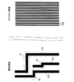
図1は、従来の半導体記憶装置における配線のレイアウトの一例を示している。この図からわかるように、同一面内に周辺領域とメモリセル領域が存在する。周辺領域の配線101,101,・・・は図中縦方向だけではなく、横方向にも走っている。即ち、周辺領域の配線101は曲げ部分(図中M部)を有している。ここで、配線101の幅は3Fである。
FIG. 1 shows an example of a wiring layout in a conventional semiconductor memory device. As can be seen from this figure, the peripheral area and the memory cell area exist in the same plane. The
一方、メモリセル領域の配線102,102,・・・は、周辺領域の配線101よりも小さいデザインルールで形成されている。即ち、配線102の幅及び配線間のスペースは、それぞれ最小値Fで形成されている。また、この図からわかるように、配線102は図中縦方向に形成されている。このように、メモリセル領域内の配線102は、最小のデザインルールで形成されるものの、曲げ部分が不要であり、直線形状で構成されることが多い。
On the other hand, the
前述のように、配線101及び102は同一面内の同じ層に形成される。従って、これらの配線101,102は、通常、図1で示したような寸法及び形状の異なる配線レイアウトを含む一枚のレチクルを用いて、1回のリソグラフィ工程を経て形成される。しかし、このリソグラフィ工程において、露光条件をメモリセル領域に最適化すると、前述のように、周辺領域の露光マージンが不足する虞がある。この問題を回避する方法の一つとして、メモリセル領域用のレチクルと周辺領域用のレチクルを別々に用意し、それぞれの領域に最適化した露光条件を用いて、2回に分けて露光することが考えられる。ただし、工程の増加によるスループットの低下及びコストの上昇という問題が新たに生じてしまう。
As described above, the
上記の技術的認識は本発明者に独自のものであり、本発明はかかる独自の技術的認識によりなされたものである。 The above technical recognition is unique to the present inventor, and the present invention has been made based on this unique technical recognition.
本発明は上記の問題を解決するために、周辺領域の配線は、メモリセル領域の配線と同じ方向に形成する。そして、配線の曲げが必要なところには、配線と異なるレイヤーに形成された接続部材を、配線間のスペースを跨ぐように形成する。これにより、同一電位となるべき隣り合う配線が電気的に接続され、所望の配線パターンが得られる。このような構成により、周辺領域の配線の走る方向を、メモリセル領域の配線の走る方向と同じにすることができ、配線のレジストパターンを形成する際、メモリセル領域に露光条件を最適化してメモリセル領域と周辺領域を一度に露光しても、周辺領域の露光マージンの不足を回避することができる。 In the present invention, in order to solve the above problem, the wiring in the peripheral region is formed in the same direction as the wiring in the memory cell region. Then, where the wiring needs to be bent, a connection member formed in a layer different from the wiring is formed so as to straddle the space between the wirings. As a result, adjacent wirings that should have the same potential are electrically connected, and a desired wiring pattern is obtained. With such a configuration, the wiring direction in the peripheral region can be made the same as the wiring direction in the memory cell region, and the exposure conditions are optimized in the memory cell region when forming the resist pattern of the wiring. Even if the memory cell area and the peripheral area are exposed at a time, it is possible to avoid an insufficient exposure margin in the peripheral area.
以下、本発明に係る3つの実施形態について図面を参照しながら説明する。同一の機能を有する構成要素には同一の符号を付し、重複する説明は適宜省略する。 Hereinafter, three embodiments according to the present invention will be described with reference to the drawings. Constituent elements having the same function are denoted by the same reference numerals, and redundant description is omitted as appropriate.
第1の実施形態及び第2の実施形態は、本発明に係る半導体装置であり、配線の曲げの必要な部分を接続部材で電気的に接続する点で共通するが、相違点の一つは、この接続部材が接続する配線の数である。即ち、第1の実施形態では、接続部材は隣り合う2本の配線を接続するのに対し、第2の実施形態では、接続部材は3本以上の配線を接続する。第3の実施形態は、使用するリソグラフィ装置の最小解像度よりも小さいパターンを形成可能な、いわゆる側壁加工プロセスにより、周辺領域の露光マージン不足を回避可能な第1及び第2の実施形態に係る半導体装置を製造する方法である。 The first embodiment and the second embodiment are semiconductor devices according to the present invention, and are common in that a portion requiring wiring bending is electrically connected by a connecting member, but one of the differences is , The number of wires connected by this connecting member. That is, in the first embodiment, the connection member connects two adjacent wires, whereas in the second embodiment, the connection member connects three or more wires. In the third embodiment, the semiconductor according to the first and second embodiments can avoid a shortage of exposure margin in the peripheral region by a so-called sidewall processing process capable of forming a pattern smaller than the minimum resolution of the lithography apparatus to be used. A method of manufacturing an apparatus.
(第1の実施形態)
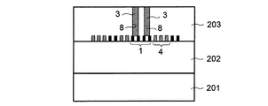
第1の実施形態について説明する。図2(a)は、本実施形態に係る半導体装置における配線のレイアウトを示している。この配線のレイアウトは、前述の図1に示す従来のレイアウトと対比できるように描かれている。図2(b)は、図2(a)のA−A線に沿う断面図である。
(First embodiment)
A first embodiment will be described. FIG. 2A shows a wiring layout in the semiconductor device according to the present embodiment. This wiring layout is drawn so as to be comparable to the conventional layout shown in FIG. FIG.2 (b) is sectional drawing which follows the AA line of Fig.2 (a).
図2(a)からわかるように、周辺領域の配線1,1,・・・及びメモリセル領域の配線2,2,・・・は、層間絶縁膜202の上に縦方向に形成されている。配線1の幅は最小値Fであり、配線2の幅及び配線2,2間のスペースは最小値Fである。なお、配線1,2の材料としては、導電性の材料、例えばタングステン、アルミニウム、銅などの金属のほか、リン又は砒素などの不純物がドーピングされたポリシリコンが用いられる。
As shown in FIG. 2A, the
また、図2(b)からわかるように、半導体基板201の上に層間絶縁膜202が形成されている。この層間絶縁膜202の上に、配線1,1,・・・および配線2,2,・・・が形成されている。隣り合う配線1,1間のスペースを跨ぐように、コンタクトホール8が層間絶縁膜202に形成されている。接続部材3は、このコンタクトホール8に導電体を埋め込んで形成されており、同一電位となるべき隣り合う配線1,1を電気的に接続している。このように、この接続部材3は実質的に従来の配線の曲げ部分の役割を果たす。なお、図2(b)に図示しないが、メモリセル領域の半導体基板201上にはメモリセルとなるトランジスタが作製され、そのトランジスタの端子と配線2が層間絶縁膜202に形成されたコンタクトプラグにより接続されている。
Further, as can be seen from FIG. 2B, an
ところで、接続部材3は配線1と異なるレイヤーに形成されているため、接続部材3は配線1と異なるレイヤーに存在する導体(例えば、半導体基板201上の配線やトランジスタの端子)と導通してしまう虞がある。このような予期せぬ電気的な接続を防止するため、図2(b)からわかるように、半導体基板201中の絶縁領域5が接続部材3に当接するように設けられている。この絶縁領域5は半導体基板201に溝を形成し、その溝に絶縁膜を埋め込んで形成されたものである。なお、この絶縁領域5は、例えば半導体基板201上に形成される素子を電気的に分離するための素子分離領域でもよい。また、半導体基板201よりも上層に接続部材3に当接する絶縁層が設けられている場合、接続部材3の底部が層間絶縁膜202中にある場合などには、この絶縁領域5は省略することができる。
By the way, since the
次に、周辺領域の配線にダミー配線を付加した変形例について、図3(a)を参照して説明する。この図からわかるように、本変形例は、図2(a)に示す周辺領域の配線レイアウトにダミー配線4,4,・・・を追加したものである。広いスペース部にダミー配線を配置することで、レジストパターンの周期性を高め、それにより、リソグラフィ工程における露光マージンの向上を図ることができる。図3(b)は、図3(a)のA−A線に沿う断面図である。
Next, a modification in which dummy wiring is added to the wiring in the peripheral region will be described with reference to FIG. As can be seen from this figure, in this modification,
次に、接続部材3の配置に関する2つの変形例について説明する。上記の説明では接続部材3は配線1の下に配置されているが、これらの変形例では、接続部材3は配線1の上に配置される。
Next, two modified examples related to the arrangement of the
一つ目の変形例を図4に示す。この図からわかるように、半導体基板201の上に、層間絶縁膜202と層間絶縁膜203が順次形成されている。層間絶縁膜202の上に配線1,1,・・・およびダミー配線4,4,・・・が形成されている。隣り合う配線1,1間のスペースを跨ぐように層間絶縁膜203を開口してコンタクトホール8が形成されている。接続部材3はこのコンタクトホール8に導電体を埋め込んで形成されている。この接続部材3は同一の電位となるべき隣り合う2つの配線1,1を電気的に接続している。なお、層間絶縁膜203上に上層配線(図示せず)が配置される場合には、配線1の電位が上層配線の影響を受けないように、接続部材3と上層配線の間の絶縁性を確保する。
A first modification is shown in FIG. As can be seen from this figure, an
二つ目の変形例を図5に示す。これは、配線1が別のレイヤーに配置された上層配線6と電気的に接続するように設計されている場合である。この図からわかるように、層間絶縁膜203上に上層配線6が形成されており、接続部材3は隣り合う配線1,1を電気的に接続すると同時に、配線1と上層配線6を電気的に接続している。なお、この上層配線6は他の配線から予期せぬ電位の影響を受けないよう配置される。
A second modification is shown in FIG. This is a case where the
なお、上記の2つの変形例においてダミー配線4は省略してもよい。
Note that the
上記のように、周辺領域の配線をメモリセル領域の配線と同じ方向の直線形状とし、曲げ部分の配線が必要となるところに曲げ部分の配線の役割を果たす接続部材を配置することで所望の配線パターンを得る。これにより、周辺領域において、露光マージンが少なくなる虞のある配線の曲げ形状を回避することができる。よって、配線のレジストパターンを形成する際、メモリセル領域に最適化した露光条件で露光する場合であっても、周辺領域の露光マージン不足を回避することができる。 As described above, the wiring in the peripheral region is formed in a straight line shape in the same direction as the wiring in the memory cell region, and the connection member that plays the role of wiring in the bent portion is disposed where the wiring in the bent portion is required. Obtain a wiring pattern. Thereby, it is possible to avoid the bent shape of the wiring that may reduce the exposure margin in the peripheral region. Therefore, when forming a resist pattern for wiring, a shortage of exposure margin in the peripheral region can be avoided even when the exposure is performed under the optimized exposure conditions for the memory cell region.
なお、上記の説明では接続部材3は、層間絶縁膜202を貫通するコンタクトホール8に導電体を埋め込んで形成されているが、層間絶縁膜202を途中まで加工して形成された溝に埋め込まれるようにしてもよい。周辺領域の配線の幅及びスペースは、Fより大きな値でもよい。
In the above description, the connecting
以上、本実施形態によれば、露光条件が最適化される領域の配線と異なる方向の配線を必要とする領域の露光マージン不足を回避することができる。 As described above, according to the present embodiment, it is possible to avoid an exposure margin shortage in a region that requires wiring in a direction different from that of a region in which the exposure condition is optimized.
(第2の実施形態)
次に、第2の実施形態について説明する。第1の実施形態との相違点の一つは、前述のように、接続部材が複数の配線間スペースを跨ぎ、3本以上の配線を電気的に接続する点である。
(Second Embodiment)
Next, a second embodiment will be described. One of the differences from the first embodiment is that, as described above, the connecting member straddles a plurality of inter-wiring spaces and electrically connects three or more wirings.
図6(a)は、本実施形態に係る半導体装置の周辺領域における配線のレイアウトを示している。この配線のレイアウトは、前述の図1に示す従来のレイアウトと対比できるように描かれている。図6(b)は、図6(a)のA−A線に沿う断面図である。 FIG. 6A shows a wiring layout in the peripheral region of the semiconductor device according to the present embodiment. This wiring layout is drawn so as to be comparable to the conventional layout shown in FIG. FIG.6 (b) is sectional drawing which follows the AA line of Fig.6 (a).
図6(a)からわかるように、第1の実施形態と同様、配線1,1,・・・及びダミー配線4,4,・・・が層間絶縁膜202上に縦方向に形成されている。配線1(4)の幅及び配線1,1(4,4)間のスペースは、ともに最小値Fである。また、図6(b)からわかるように、コンタクトホール9は複数の配線1,1間スペースを跨ぐように形成されている。接続部材7は、このコンタクトホール9に導電体を埋め込むことにより形成されており、同一電位となるべき4本の配線1,1,1,1を電気的に接続している。このように、接続部材7は実質的に従来の配線の曲げ部分の役割を果たす。
6A, the
本実施形態に係る半導体装置におけるメモリセル領域の配線レイアウトは、第1の実施形態(図2(a))と同じである。 The wiring layout of the memory cell region in the semiconductor device according to the present embodiment is the same as that of the first embodiment (FIG. 2A).
なお、上記の説明では接続部材7は、層間絶縁膜202を貫通するコンタクトホール9に埋め込まれているが、層間絶縁膜202を途中まで加工して形成された溝に埋め込まれるようにしてもよい。また、周辺領域の配線の幅及びスペースは、Fより大きな値でもよい。ダミー配線4,4,・・・を省略してもよい。また、接続部材7は、第1の実施形態において図4及び図5を用いて説明したように、配線1の上側に作成してもよい。この際、無関係の配線などから予期しない電位の影響を受けないように、接続部材7を配置する点も同様である。
In the above description, the connecting
上記のように、本実施形態では、複数の配線間スペースに跨るように接続部材7を形成することにより、第1の実施形態と同じ作用効果を奏するのに加えて、配線間の接続がオープン不良になるリスクを低減することができる。さらに、コンタクトホール9が横長の形状のため、接続すべき隣接配線間のスペースが長い場合でも容易に対応できる。
As described above, in this embodiment, the
以上、本実施形態によれば、露光条件が最適化される領域の配線と異なる方向の配線を必要とする領域の露光マージン不足を回避することができる。 As described above, according to the present embodiment, it is possible to avoid an exposure margin shortage in a region that requires wiring in a direction different from that of a region in which the exposure condition is optimized.
(第3の実施形態)
次に、第3の実施形態について説明する。本実施形態は、前述のように、使用するリソグラフィ装置の最小解像度よりも小さいパターンを形成可能な、いわゆる側壁加工プロセスにより、第1及び第2の実施形態に係る半導体装置を製造する方法である。
(Third embodiment)
Next, a third embodiment will be described. As described above, the present embodiment is a method of manufacturing the semiconductor device according to the first and second embodiments by a so-called sidewall processing process capable of forming a pattern smaller than the minimum resolution of the lithography apparatus to be used. .
周辺領域の配線パターンを最小デザインルールで形成する場合、使用するリソグラフィ装置の最小解像度がF以下であれば、以下の手法を用いて、最小デザインルールに従う所望の配線を得ることができるので問題ない。即ち、層間絶縁膜202及び接続部材3(7)の上に導電膜とレジストを順次形成し、露光・現像により幅及びスペースがFのレジストパターンを形成し、その後、このレジストパターンをマスクとして導電膜をエッチングすればよい。しかし、近年、使用するリソグラフィ装置の最小解像度よりも小さいデザインルールを採用する場合が出てきている。本実施形態は、そのような場合であっても、周辺領域の露光マージン不足を回避可能な第1及び第2の実施形態に係る半導体装置を製造することができるようにするものである。
When forming the wiring pattern of the peripheral region with the minimum design rule, if the minimum resolution of the lithography apparatus to be used is F or less, there is no problem because a desired wiring according to the minimum design rule can be obtained using the following method. . That is, a conductive film and a resist are sequentially formed on the
以下、図7(a)〜図14を参照して、本実施形態に係る半導体装置の製造方法を説明する。なお、図7(b)〜図12(b)は、それぞれ図7(a)〜図12(a)のC−D線に沿う端面図である。図7(a)〜図14は、周辺領域の平面図、端面図を示している。メモリセル領域の配線形成のプロセスは周辺領域と同時に進み、接続部材が無い他は周辺領域と同様である。 Hereinafter, with reference to FIGS. 7A to 14, a method for manufacturing the semiconductor device according to the present embodiment will be described. In addition, FIG.7 (b)-FIG.12 (b) are the end elevations which follow the CD line | wire of Fig.7 (a)-FIG.12 (a), respectively. 7A to 14 show a plan view and an end view of the peripheral region. The process of forming the wiring in the memory cell area proceeds simultaneously with the peripheral area, and is the same as the peripheral area except that there is no connection member.
(1)半導体基板201を加工して所定の位置に溝を形成し、この溝に絶縁膜を埋込み、絶縁領域5を形成する。次いで、半導体基板201及び絶縁領域5上に層間絶縁膜202を形成し、この層間絶縁膜202の所定の位置を開口してコンタクトホール9を形成する。次いで、このコンタクトホール9に導電体を埋め込むことにより接続部材7を形成する。なお、図7(b)からわかるように、絶縁領域5は接続部材7に当接するように形成されている。
(2)次に、図7(b)に示すように、層間絶縁膜202と接続部材7の上に、
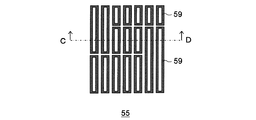
導電膜58、第1マスク材57、第2マスク材56、第3マスク材55、第4マスク材54、第5マスク材53を順次形成する。各マスク材の材料として、例えば、第1マスク材57はシリコン窒化膜、第2マスク材56はシリコン酸化膜、第3マスク材55はシリコン窒化膜、第4マスク材54はTEOS膜、第5マスク材はポリシリコン膜をそれぞれ用いることができる。
なお、第2マスク材56は、後の工程において除去を容易にするため、BSG膜を使用してもよい。また、導電膜58の材料としては、導電性の材料、例えばタングステン、アルミニウム、銅などの金属のほか、リン又は砒素などの不純物がドーピングされたポリシリコンが用いられる。
(3)次に、第5マスク材53の上にレジスト膜を形成し、リソグラフィによりレジスト51、52からなるレジストパターンを形成する。このレジストパターンの幅とスペースは、それぞれ最小デザインルールの2倍である2Fである。この際、レジストパターンはメモリセル領域と周辺領域で同じ方向(図中縦方向)に沿って走っているため、メモリセル領域に露光条件を最適化しても、周辺領域の露光マージン不足を回避することができる。図7(a)にこのレジストパターンの平面図を示す。図7(a)中、レジスト51(輪郭線が実線)は最終的に使用する配線になる部分であり、レジスト52(輪郭線が破線)は最終的にダミー配線となる部分である。なお、レジスト52は省略してもよい。
(4)次に、レジスト51,52をマスクにして、第5マスク材53をエッチングし、その後、アッシングによりレジスト51,52を除去する。ここで、アッシングに加えて、硫酸と過酸化水素水の混合液による処理を行うことによりレジストを除去してもよい。
(5)次に、ポリシリコン膜53をマスクにして、第4マスク材54をエッチングする。図8(a)と図8(b)はエッチング後の平面図及び端面図をそれぞれ示している。図8(a)において、レジスト51と52の位置に対応する第5マスク材は、それぞれ第5マスク材53と53’として区別して表記されている。エッチング前の第4マスク材54のパターンは、レジスト51, 52をそのまま引き継いでいるため、幅及びスペースは共に2F、つまりピッチは4Fである。
(6)次に、第4マスク材54のパターンを、フッ化アンモニウム水溶液等を用いたウェットエッチングにより細らせる。この際、第4マスク材54のパターンの幅がF、スペースが3Fになるように処理条件を設定する。
(7)次に、ウェットエッチングまたはRIEを用いて第5マスク材53を除去する。除去後の平面図及び端面図を図9(a)及び図9(b)にそれぞれ示す。
(8)次に、第3マスク材55及び第4マスク材54の上に、例えば、ポリシリコンからなる第6マスク材を堆積し、その後、異方性エッチングにより第4マスク材54の側部に第6マスク材が残るように加工する。これにより、第4マスク材54の側壁に第1環状マスク材59が形成される。この第1環状マスク材59の幅(膜厚)がFになるように、堆積する第6マスク材の厚さ及びエッチバック条件を設定する。エッチバック後の平面図及び端面図を図10(a)及び図10(b)にそれぞれ示す。
(9)次に、フッ化アンモニウム水溶液などを用いて第4マスク材54を除去する。除去後の平面図及び端面図を図11(a)及び図11(b)にそれぞれ示す。第1環状マスク材59の幅及びスペースは、この段階で2FではなくてFになっている。なお、第4マスク材54の下に第3マスク材55があるため、第4マスク材54を除去する際、フッ化アンモニウム水溶液は第3マスク材55には浸透せず、第3マスク材55の下の層には影響がない。
(10)以降、第1環状マスク材59をマスクにして第3マスク材55より下の膜を順次エッチングしていく。最終的には、第2マスク材56を犠牲膜にして導電膜58を加工し、環状導電膜61を形成する。その後、第2マスク材56を除去する。除去後の平面図及び端面図を図12(a)及び図12(b)にそれぞれ示す。これらの図からわかるように、環状導電膜61の幅及びスペースは共にFである。また、図12(b)からわかるように、層間絶縁膜202中の接続部材7により、左右両端の環状導電膜61,61が電気的に接続されている。つまり、接続部材7は、第1及び第2の実施形態と同様に、従来の配線の曲げ部分の役割を果たす。
(11)次に、層間絶縁膜202、接続部材7及び環状に加工された第1マスク材57からなる第2環状マスク材60の上にレジスト膜を形成した後、リソグラフィにより、このレジスト膜のうち環状導電膜61の端部に対応する部分を開口する。図13中のA部は、レジストを開口する部分を示している。
(12)次に、開口した部分の第2環状マスク材60と環状導電膜61を、RIEなどによりエッチングして除去し、環状導電膜61の端部を切断する。その後、レジスト膜を除去する。
(13)最後に、第2環状マスク材60を除去し、図14に示すように配線1,1,・・・が完成する。配線1の幅及び配線間のスペースは共にFである。なお、図示しないが、メモリセル領域においても、幅及び配線間のスペースが共にFの配線2,2,・・・が完成する。
なお、上記では複数の配線間スペースを跨ぐ接続部材7を有する半導体装置の製造方法について説明したが、一つの配線間スペースを跨ぐ接続部材3を層間絶縁膜202中に複数形成しておくことで、第1の実施形態に係る半導体装置を製造することも可能である。また、側壁加工プロセスにより配線を形成した後に、配線の上に形成された層間絶縁膜中に接続部材を形成して、第1の実施形態で説明した変形例(図4、図5参照)に係る半導体装置を製造してもよい。
また、本実施形態は上記の側壁加工プロセスに限定されるものではない。例えば、上記の製造方法において、第2マスク材56及び第1マスク材57を省く場合もある。その他、当業者の用いうる側壁加工プロセスを使用することができる。
(1) The
(2) Next, as shown in FIG. 7B, on the
The
The
(3) Next, a resist film is formed on the
(4) Next, the
(5) Next, the
(6) Next, the pattern of the
(7) Next, the
(8) Next, a sixth mask material made of, for example, polysilicon is deposited on the
(9) Next, the
(10) Thereafter, the film below the
(11) Next, after a resist film is formed on the
(12) Next, the second
(13) Finally, the second
In the above description, the manufacturing method of the semiconductor device having the
Further, the present embodiment is not limited to the above sidewall processing process. For example, in the above manufacturing method, the
以上、本実施形態によれば、メモリセル領域に露光条件を最適化する場合でも周辺領域の露光マージン不足を防ぎ、かつ、リソグラフィの最小解像度よりも小さいデザインルールに従う配線を有する半導体装置を製造することができる。 As described above, according to the present embodiment, even when the exposure conditions are optimized in the memory cell region, a shortage of exposure margin in the peripheral region is prevented, and a semiconductor device having wiring conforming to a design rule smaller than the minimum resolution of lithography is manufactured. be able to.
第1乃至第3の実施形態について説明した。上記の説明では、半導体装置としてメモリセル領域とそれ以外の周辺領域を有する半導体記憶装置を想定したが、本発明はこれに限定されるものではない。本発明は、一般に、特定方向に沿って走る複数の配線を有する領域と、この領域の配線とは異なる方向の配線を必要する別の領域とを、同一面内に有する半導体装置に適用可能である。 The first to third embodiments have been described. In the above description, a semiconductor memory device having a memory cell region and other peripheral regions is assumed as the semiconductor device, but the present invention is not limited to this. The present invention is generally applicable to a semiconductor device having a region having a plurality of wirings running along a specific direction and another region requiring wiring in a direction different from the wirings in this region in the same plane. is there.
1,2・・・配線、3,7・・・接続部材、4・・・ダミー配線、5・・・絶縁領域、6・・・上層配線、8,9・・・コンタクトホール、51,52・・・レジスト、53,53’・・・第5マスク材、54,54’・・・第4マスク材、55・・・第3マスク材、56・・・第2マスク材、57・・・第1マスク材、58・・・導電膜、59・・・第1環状マスク材、60・・・第2環状マスク材、61・・・環状導電膜、101,102・・・配線、201・・・半導体基板、202,203・・・層間絶縁膜、M・・・配線の曲げ部分、A・・・レジスト膜の開口部分(端部) 1, 2 ... wiring, 3, 7 ... connecting member, 4 ... dummy wiring, 5 ... insulating region, 6 ... upper layer wiring, 8, 9 ... contact hole, 51, 52 ... Resist, 53, 53 '... Fifth mask material, 54,54' ... Fourth mask material, 55 ... Third mask material, 56 ... Second mask material, 57 ... First mask material, 58 ... conductive film, 59 ... first annular mask material, 60 ... second annular mask material, 61 ... annular conductive film, 101, 102 ... wiring, 201 ... Semiconductor substrate, 202, 203 ... interlayer insulating film, M ... bending part of wiring, A ... opening part (end part) of resist film
Claims (5)
前記半導体基板上に形成された層間絶縁膜と、
前記層間絶縁膜上の第1の領域において、第1のデザインルールを適用して形成された、特定方向に沿って走る、複数の第1の配線と、
前記層間絶縁膜上の第2の領域において、前記第1のデザインルールと同じ第2のデザインルールを適用して形成された、前記特定方向に沿って走る、複数の第2の配線と、
前記層間絶縁膜中に形成され、同一電位となるべき少なくとも2つの前記第2の配線を電気的に接続して所望の配線パターンを形成する、接続部材と、
を備えることを特徴とする半導体装置。 A semiconductor substrate;
An interlayer insulating film formed on the semiconductor substrate;
In the first region on the interlayer insulating film, a plurality of first wirings formed by applying a first design rule and running along a specific direction;
In the second region on the interlayer insulating film, a plurality of second wirings that are formed by applying a second design rule that is the same as the first design rule and that run along the specific direction;
A connecting member formed in the interlayer insulating film and electrically connecting at least two second wirings to be at the same potential to form a desired wiring pattern;
A semiconductor device comprising:
前記半導体基板に形成された絶縁領域をさらに備え、
前記接続部材は、前記絶縁領域と当接して、前記半導体基板上の導体から絶縁されていることを特徴とする半導体装置。 The semiconductor device according to claim 1,
Further comprising an insulating region formed in the semiconductor substrate;
The connection member is in contact with the insulating region and insulated from a conductor on the semiconductor substrate.
前記半導体基板上に形成された第1の層間絶縁膜と、
前記第1の層間絶縁膜上の第1の領域において、第1のデザインルールを適用して形成された、特定方向に沿って走る、複数の第1の配線と、
前記第1の層間絶縁膜上の第2の領域において、前記第1のデザインルールと同じ第2のデザインルールを適用して形成された、前記特定方向に沿って走る、複数の第2の配線と、
前記第1の層間絶縁膜の上に形成された第2の層間絶縁膜と、
前記第2の層間絶縁膜中に形成され、同一電位となるべき少なくとも2つの前記第2の配線を電気的に接続して所望の配線パターンを形成する、接続部材と、
を備えることを特徴とする半導体装置。 A semiconductor substrate;
A first interlayer insulating film formed on the semiconductor substrate;
In the first region on the first interlayer insulating film, a plurality of first wirings formed by applying a first design rule and running along a specific direction;
In the second region on the first interlayer insulating film, a plurality of second wirings that are formed by applying the same second design rule as the first design rule and run along the specific direction When,
A second interlayer insulating film formed on the first interlayer insulating film;
A connecting member formed in the second interlayer insulating film and electrically connecting at least two second wirings to be at the same potential to form a desired wiring pattern;
A semiconductor device comprising:
メモリセルアレイを構成する複数のメモリセルと、前記メモリセルを駆動する駆動素子と、をさらに備え、
前記第1の配線はビット線であり、前記第2の配線は前記メモリセルと前記駆動素子を接続するための配線である、
ことを特徴とする半導体装置。 A semiconductor device according to any one of claims 1 to 3,
A plurality of memory cells constituting a memory cell array; and a drive element for driving the memory cells,
The first wiring is a bit line, and the second wiring is a wiring for connecting the memory cell and the driving element.
A semiconductor device.
半導体基板上に前記層間絶縁膜を形成し、
前記第2の領域において、前記層間絶縁膜の所定の位置にコンタクトホールを形成した後、前記コンタクトホールに前記接続部材を埋め込み、
前記層間絶縁膜及び前記接続部材の上に導電膜を形成し、
前記導電膜よりも上方にマスク材を形成し、
リソグラフィにより前記マスク材を、前記デザインルールの2倍の幅及びスペースのパターンに加工し、
ウェットエッチングにより前記マスク材の前記パターンの幅が半分になるまで、前記マスク材をエッチングし、
その後、前記マスク材の側壁に前記マスク材を囲うように、前記デザインルールと同じ寸法の膜厚を持つ環状マスク材を形成し、
その後、前記マスク材を除去して、前記環状マスク材をマスクとして前記導電膜をエッチングして環状導電膜を形成し、
前記環状導電膜の端部をエッチングすることにより、前記複数の第1の配線及び前記複数の第2の配線を形成する、
ことを特徴とする半導体装置の製造方法。 A plurality of first wirings in the first region and a plurality in the second region, which are formed by applying a design rule smaller than the minimum resolution of the lithographic apparatus and run along the same direction, on the interlayer insulating film A method of manufacturing a semiconductor device, wherein a wiring having the same potential among the plurality of second wirings is electrically connected by a connecting member to form a desired wiring pattern. There,
Forming the interlayer insulating film on a semiconductor substrate;
In the second region, after forming a contact hole at a predetermined position of the interlayer insulating film, the connection member is embedded in the contact hole,
Forming a conductive film on the interlayer insulating film and the connection member;
Forming a mask material above the conductive film;
The mask material is processed into a pattern having a width and space twice the design rule by lithography,
Etching the mask material until the pattern width of the mask material is halved by wet etching,
Thereafter, an annular mask material having a film thickness of the same dimensions as the design rule is formed so as to surround the mask material on the side wall of the mask material,
Then, the mask material is removed, and the conductive film is etched using the annular mask material as a mask to form an annular conductive film,
Etching the annular conductive film to form the plurality of first wirings and the plurality of second wirings;
A method for manufacturing a semiconductor device.
Priority Applications (2)
| Application Number | Priority Date | Filing Date | Title |
|---|---|---|---|
| JP2008222197A JP2010056439A (en) | 2008-08-29 | 2008-08-29 | Semiconductor device and method of manufacturing same |
| US12/546,383 US8304910B2 (en) | 2008-08-29 | 2009-08-24 | Semiconductor device and method of producing the same |
Applications Claiming Priority (1)
| Application Number | Priority Date | Filing Date | Title |
|---|---|---|---|
| JP2008222197A JP2010056439A (en) | 2008-08-29 | 2008-08-29 | Semiconductor device and method of manufacturing same |
Publications (1)
| Publication Number | Publication Date |
|---|---|
| JP2010056439A true JP2010056439A (en) | 2010-03-11 |
Family
ID=41724111
Family Applications (1)
| Application Number | Title | Priority Date | Filing Date |
|---|---|---|---|
| JP2008222197A Abandoned JP2010056439A (en) | 2008-08-29 | 2008-08-29 | Semiconductor device and method of manufacturing same |
Country Status (2)
| Country | Link |
|---|---|
| US (1) | US8304910B2 (en) |
| JP (1) | JP2010056439A (en) |
Cited By (1)
| Publication number | Priority date | Publication date | Assignee | Title |
|---|---|---|---|---|
| JP2014103294A (en) * | 2012-11-21 | 2014-06-05 | Dainippon Printing Co Ltd | Imprint mold and method for manufacturing imprint mold, method for forming pattern, and method for manufacturing semiconductor device |
Families Citing this family (2)
| Publication number | Priority date | Publication date | Assignee | Title |
|---|---|---|---|---|
| KR101123804B1 (en) * | 2009-11-20 | 2012-03-12 | 주식회사 하이닉스반도체 | Semiconductor chip and stacked semiconductor package havng the same |
| US9589974B2 (en) | 2013-09-11 | 2017-03-07 | Kabushiki Kaisha Toshiba | Nonvolatile semiconductor memory device and method for manufacturing same |
Family Cites Families (5)
| Publication number | Priority date | Publication date | Assignee | Title |
|---|---|---|---|---|
| JP2990870B2 (en) * | 1991-07-18 | 1999-12-13 | 松下電器産業株式会社 | Semiconductor integrated circuit device and method of manufacturing the same |
| JP3109478B2 (en) | 1998-05-27 | 2000-11-13 | 日本電気株式会社 | Semiconductor device |
| JP3534674B2 (en) | 1999-03-26 | 2004-06-07 | 沖電気工業株式会社 | Aperture and exposure method using the same |
| JP3434780B2 (en) | 2000-04-25 | 2003-08-11 | Necエレクトロニクス株式会社 | Semiconductor device |
| KR100568515B1 (en) * | 2004-12-06 | 2006-04-07 | 삼성전자주식회사 | Semiconductor device having a resistor and fabrication methods thereof |
-
2008
- 2008-08-29 JP JP2008222197A patent/JP2010056439A/en not_active Abandoned
-
2009
- 2009-08-24 US US12/546,383 patent/US8304910B2/en active Active
Cited By (1)
| Publication number | Priority date | Publication date | Assignee | Title |
|---|---|---|---|---|
| JP2014103294A (en) * | 2012-11-21 | 2014-06-05 | Dainippon Printing Co Ltd | Imprint mold and method for manufacturing imprint mold, method for forming pattern, and method for manufacturing semiconductor device |
Also Published As
| Publication number | Publication date |
|---|---|
| US8304910B2 (en) | 2012-11-06 |
| US20100052182A1 (en) | 2010-03-04 |
Similar Documents
| Publication | Publication Date | Title |
|---|---|---|
| US8835314B2 (en) | Method for fabricating semiconductor memory device | |
| US20110062552A1 (en) | Semiconductor device | |
| CN107154345B (en) | Photomask pattern and method of forming fine pattern | |
| US8164119B2 (en) | Semiconductor device including conductive lines with fine line width and method of fabricating the same | |
| US8513809B2 (en) | Semiconductor device | |
| JP4901898B2 (en) | Manufacturing method of semiconductor device | |
| US8728898B2 (en) | Method for fabricating semiconductor device | |
| JP2005026641A (en) | Semiconductor device and method of manufacturing same | |
| JP2009060074A (en) | Method for forming contact of semiconductor device | |
| JP2008187178A (en) | Semiconductor device and method of manufacturing the same | |
| JP2010056439A (en) | Semiconductor device and method of manufacturing same | |
| US20140008808A1 (en) | Method for fabricating a semiconductor device with formation of conductive lines | |
| US11804381B2 (en) | Conductive wire structure | |
| JP2008205122A (en) | Semiconductor device and its manufacturing method | |
| US10795255B2 (en) | Method of forming layout definition of semiconductor device | |
| JP5881569B2 (en) | Pattern formation method | |
| KR20100111468A (en) | Method of manufacturing semiconductor device | |
| US7160794B1 (en) | Method of fabricating non-volatile memory | |
| JP2014241325A (en) | Semiconductor device and semiconductor device manufacturing method | |
| US20080153289A1 (en) | Method for manufacturing semiconductor devices and plug | |
| US9349813B2 (en) | Method for fabricating semiconductor device | |
| US20080233727A1 (en) | Method of manufacturing semiconductor device | |
| KR100973266B1 (en) | Method of manufacturing of semiconductor | |
| JP2011009625A (en) | Method of manufacturing semiconductor device | |
| JP2008218638A (en) | Semiconductor device and its manufacturing method |
Legal Events
| Date | Code | Title | Description |
|---|---|---|---|
| A621 | Written request for application examination |
Free format text: JAPANESE INTERMEDIATE CODE: A621 Effective date: 20100910 |
|
| A762 | Written abandonment of application |
Free format text: JAPANESE INTERMEDIATE CODE: A762 Effective date: 20120516 |