JP2010056433A - Method of manufacturing flat panel display device - Google Patents
Method of manufacturing flat panel display device Download PDFInfo
- Publication number
- JP2010056433A JP2010056433A JP2008222063A JP2008222063A JP2010056433A JP 2010056433 A JP2010056433 A JP 2010056433A JP 2008222063 A JP2008222063 A JP 2008222063A JP 2008222063 A JP2008222063 A JP 2008222063A JP 2010056433 A JP2010056433 A JP 2010056433A
- Authority
- JP
- Japan
- Prior art keywords
- amorphous silicon
- display device
- laser beam
- manufacturing
- laser
- Prior art date
- Legal status (The legal status is an assumption and is not a legal conclusion. Google has not performed a legal analysis and makes no representation as to the accuracy of the status listed.)
- Pending
Links
Images


Abstract
Description
本発明は、平面表示装置の製造方法に関し、特に、平面表示装置内での特性バラツキが小さいTFT素子を有する平面表示装置の製造方法に適用して有効な技術に関するものである。 The present invention relates to a method for manufacturing a flat display device, and more particularly to a technique that is effective when applied to a method for manufacturing a flat display device having TFT elements with small characteristic variations in the flat display device.
従来、一対の基板の間に液晶材料を封入した液晶表示パネルを有する液晶表示装置には、アクティブマトリクス型のTFT液晶表示装置がある。アクティブマトリクス型のTFT液晶表示装置は、たとえば、テレビ受像器やパーソナル・コンピュータ(PC)のディスプレイ、携帯電話端末や携帯情報端末(PDA)の表示部などに広く用いられている。 Conventionally, a liquid crystal display device having a liquid crystal display panel in which a liquid crystal material is sealed between a pair of substrates includes an active matrix TFT liquid crystal display device. An active matrix TFT liquid crystal display device is widely used, for example, in a television receiver, a display of a personal computer (PC), a display unit of a mobile phone terminal or a personal digital assistant (PDA).
アクティブマトリクス型のTFT液晶表示装置で用いられる液晶表示パネルは、一方の基板に、複数本の走査信号線、複数本の映像信号線、TFT素子、画素電極などが設けられている。従来の液晶表示装置は、たとえば、複数本の映像信号線に映像信号(階調データと呼ぶこともある)を入力するためのドライバICや、複数本の走査信号線に走査信号を入力するためのドライバICが実装されたTCPやCOFなどのフレキシブル回路基板を液晶表示パネルに接続したり、前記各ドライバICを直接液晶表示パネル上に実装しているのが一般的である。また、近年は、たとえば、前記走査信号線などが形成された基板(以下、TFT基板と呼ぶ)の表示領域の外側に、前記ドライバICと同等の機能を有する駆動回路(周辺回路)を形成した液晶表示パネルが提案されている。 In a liquid crystal display panel used in an active matrix TFT liquid crystal display device, a plurality of scanning signal lines, a plurality of video signal lines, TFT elements, pixel electrodes, and the like are provided on one substrate. In a conventional liquid crystal display device, for example, a driver IC for inputting a video signal (sometimes referred to as gradation data) to a plurality of video signal lines or a scanning signal to a plurality of scanning signal lines is input. In general, a flexible circuit board such as TCP or COF on which a driver IC is mounted is connected to a liquid crystal display panel, or each of the driver ICs is mounted directly on the liquid crystal display panel. In recent years, for example, a drive circuit (peripheral circuit) having a function equivalent to that of the driver IC is formed outside a display region of a substrate (hereinafter referred to as a TFT substrate) on which the scanning signal lines are formed. Liquid crystal display panels have been proposed.
前記TFT基板の表示領域の外側に形成される前記駆動回路は、主に、トランジスタやダイオードなどの半導体素子で構成されており、前記走査信号線や前記映像信号線を形成する際に各半導体素子の電極を形成し、表示領域のTFT素子の半導体層(チャネル層)を形成する際に半導体素子の半導体層を形成する。TFT基板の表示領域に形成するTFT素子の半導体層は、アモルファスシリコン(a−Si:非晶質シリコン)では動特性の面で不十分な場合がある。このため、半導体層としてのアモルファスシリコンを結晶化する必要がある。 The drive circuit formed outside the display area of the TFT substrate is mainly composed of semiconductor elements such as transistors and diodes, and each semiconductor element is formed when forming the scanning signal lines and the video signal lines. The semiconductor layer of the semiconductor element is formed when the semiconductor layer (channel layer) of the TFT element in the display region is formed. The semiconductor layer of the TFT element formed in the display region of the TFT substrate may be insufficient in terms of dynamic characteristics when using amorphous silicon (a-Si: amorphous silicon). For this reason, it is necessary to crystallize amorphous silicon as a semiconductor layer.
近年、アモルファスシリコン膜にレーザを照射して結晶化させる技術が確立され、製品に適用されている。一般的には、電気炉などでの450度、数時間の熱処理によりアモルファスシリコンを脱水素化し、脱水素化したアモルファスシリコンに対してエキシマレーザなどのパルスレーザを1箇所に対して複数回照射されるように少しずつステップ移動させながら照射することで、基板上のアモルファスシリコン膜を多結晶化する方法が採用されている。中でも、連続発振レーザ光を線状あるいは矩形状に整形・集光し、ビームの短軸幅方向に走査することで得られる帯状多結晶膜で構成したTFTは、パルスレーザで形成された結晶で構成されたTFTより動特性の面で格段に優れている。 In recent years, a technique for crystallizing an amorphous silicon film by irradiating a laser has been established and applied to products. In general, amorphous silicon is dehydrogenated by heat treatment in an electric furnace or the like at 450 ° C. for several hours, and a pulse laser such as an excimer laser is irradiated to the dehydrogenated amorphous silicon a plurality of times. In this way, a method is employed in which the amorphous silicon film on the substrate is polycrystallized by irradiating while moving step by step. Above all, TFTs composed of a strip-like polycrystalline film obtained by shaping and condensing continuous wave laser light into a linear or rectangular shape and scanning in the direction of the minor axis width of the beam are crystals formed by a pulsed laser. It is much better in terms of dynamic characteristics than the constructed TFT.
しかし、これらの方法で形成された多結晶シリコンには以下に述べる問題点がある。即ち、エキシマレーザなどのパルスレーザ照射で得られた多結晶シリコンは、結晶粒径が数100nm〜数μmであり、TFTのチャネル領域に含まれる結晶粒界の数によって特性が大きく変動する。また、パルスレーザ照射による多結晶膜は粒界部に突起が形成されやすく、トップゲート構造のTFTにおいてはこれらの突起がゲート絶縁膜の耐圧を低下させる原因にもなる。また、連続発振レーザ光の走査で得られた帯状多結晶膜はレーザ光の走査方向(結晶の成長方向)に対しては大きな移動度が得られるが、走査方向と直行する方向には移動度が半減するなど、特性の方向依存性が大きいことが問題であった。 However, the polycrystalline silicon formed by these methods has the following problems. That is, polycrystalline silicon obtained by irradiation with a pulsed laser such as an excimer laser has a crystal grain size of several hundred nm to several μm, and its characteristics greatly vary depending on the number of crystal grain boundaries included in the channel region of the TFT. In addition, the polycrystalline film formed by the pulse laser irradiation is prone to have protrusions at the grain boundary portions, and in the top gate structure TFT, these protrusions also cause the breakdown voltage of the gate insulating film to decrease. In addition, the band-like polycrystalline film obtained by scanning with continuous wave laser light has a large mobility in the scanning direction of laser light (crystal growth direction), but the mobility is perpendicular to the scanning direction. The problem is that the direction dependency of the characteristics is large, such as halving.
この問題に対処する方法として、結晶粒径が100nm以下の多結晶シリコン膜(微結晶シリコン膜)でTFTのチャネル層を構成する方法が、例えば特許文献1に開示されている。
As a method for coping with this problem, for example,
特許文献1は、基板上にゲート電極を形成し、ゲート電極を被覆するようにゲート絶縁膜、非晶質シリコン膜、バッファー膜、光−熱変換膜の順で成膜して、光−熱変換膜に半導体レーザ光を照射して非晶質シリコン膜を微結晶シリコン膜に結晶化した後、光−熱変換膜とバッファー膜を除去し、微結晶シリコン膜上に非晶質シリコン膜を成膜し、更にソース・ドレイン電極を形成することで薄膜トランジスタを製造する方法を開示している。
In
本発明は、上記従来技術を改良するものである。即ち、特許文献1に記載された方法は、非晶質シリコン膜上に本来は不要なバッファー膜と光−熱変換膜を形成し、レーザ照射により前記非晶質シリコン膜を微結晶化した後、バッファー膜と光−熱変換膜を除去するなど、余分な工程が含まれ、製造コスト増大・スループット低下の原因となる問題があった。
The present invention improves the above-described prior art. That is, in the method described in
本発明の目的は、バッファー膜や光−熱変換膜の成膜および除去の工程を不要とし、特性バラツキが小さく、方向依存性のないTFTを有する平面表示装置を低コスト、高歩留まりで製造する方法を提供することにある。 An object of the present invention is to manufacture a flat display device having TFTs with little variation in characteristics and having no direction dependency by eliminating the process of forming and removing a buffer film and a light-heat conversion film at low cost and high yield. It is to provide a method.
上記目的を達成するために、本発明の平面表示装置の製造方法は連続発振レーザ光を一方向に均一なエネルギ密度分布を有する線状あるいは矩形状のビームに整形し、前記ビームを投影光学系により非晶質シリコン膜表面に投影することで直接照射し、一方向と直交する方向に相対的に走査する。その際、照射するレーザの波長として照射対象となる非晶質シリコン膜厚に十分透過して膜全体を一様に加熱でき、かつ多結晶膜シリコンより非晶質シリコンの吸収係数が大きい波長が選択される。また、非晶質シリコン膜が溶融せずかつ融点に近い温度に一定時間保たれるようにレーザ光が照射される。これにより、非晶質シリコン膜が厚さ方向に一様に、かつ一定時間加熱され、安定に微結晶シリコン膜に変換される。 In order to achieve the above object, the flat display device manufacturing method of the present invention shapes a continuous wave laser beam into a linear or rectangular beam having a uniform energy density distribution in one direction, and projects the beam into a projection optical system. Thus, direct irradiation is performed by projecting onto the surface of the amorphous silicon film, and scanning is performed relatively in a direction orthogonal to one direction. At that time, the wavelength of the laser to be irradiated can be sufficiently transmitted through the amorphous silicon film thickness to be irradiated to uniformly heat the entire film, and the wavelength of the absorption coefficient of amorphous silicon is larger than that of polycrystalline silicon. Selected. Further, the laser beam is irradiated so that the amorphous silicon film is not melted and is kept at a temperature close to the melting point for a certain time. As a result, the amorphous silicon film is heated uniformly in the thickness direction for a predetermined time, and is stably converted into a microcrystalline silicon film.
本発明により、バッファー膜や光−熱変換膜の成膜および除去の工程を不要とし、特性バラツキが小さく、特性の方向依存性がないTFTを有する平面表示装置を低コスト、高歩留まりで製造することができる。 According to the present invention, a flat display device having a TFT with no characteristic variation and no direction dependency of characteristics is manufactured at low cost and with a high yield without the need for forming and removing a buffer film and a light-heat conversion film. be able to.
以下、本発明の最良の実施形態につき、図面を参照して詳細に説明する。 DESCRIPTION OF THE PREFERRED EMBODIMENTS Hereinafter, the best embodiment of the present invention will be described in detail with reference to the drawings.
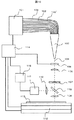
図1は本発明である平面表示装置の製造方法を実施するに好適なレーザ微結晶化装置の光学系構成を示す図である。励起用LD(レーザダイオード)1とファイバ2で結合された連続発振レーザ光3を発生するレーザ発振器4、レーザ光3の必要時以外の遮蔽を行なうシャッタ5、レーザ光3のエネルギを調整するための透過率連続可変NDフィルタ6、レーザ光3を振幅変調してパルス化あるいはエネルギの時間的な変調を実現するための変調器7、レーザ光3のビーム径を調整するためのビームエキスパンダ(あるいはビームリデューサ)9、レーザ光3をトップフラットな矩形状ビームに整形するビーム整形器10、整形されたレーザ光3の寸法を調整するための矩形スリット11、ビーム整形器10および矩形スリット11で矩形状に整形されたレーザビームをXYステージ12上に載置された基板13上に縮小投影する投影レンズ14、基板13の観察あるいはアライメントマーク検出などを行なうためのダイクロイックミラー15、結像レンズ16、CCDカメラ17、画像処理装置18、励起用LD1のON/OFF、シャッタ5の開閉、透過率連続可変NDフィルタ6の透過率調整、変調器7のON/OFF、ステージ12の駆動、画像処理装置18によるアライメントマークの検出、および必要に応じてビーム整形器10、20の切り替えなどを制御する制御装置19から構成されている。
FIG. 1 is a diagram showing an optical system configuration of a laser microcrystallization apparatus suitable for carrying out the flat display device manufacturing method according to the present invention. In order to adjust the energy of the laser beam 3, a
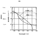
次に、各部の動作・機能について詳細に説明する。まず照射するレーザ光の波長について考える。図2に非晶質シリコンと結晶シリコンの分光吸収係数(α)を示す。横軸は波長(nm)、縦軸は吸収係数α(cm−1)である。非晶質シリコン膜を微結晶化するには非晶質シリコン薄膜に対して吸収のある波長を照射する必要がある。しかし、吸収係数が大きすぎるとレーザ光は非晶質シリコン膜を透過できずに表面のみ加熱される。当然、熱伝導により基板と接する側まで加熱されるが、表面とは温度が異なり結晶化の状態も異なるため、好ましくない。即ち、レーザ光の浸透深さ(吸収係数の逆数)が非晶質シリコン膜の膜厚程度以上であることが望ましい。例えば非晶質シリコン膜の膜厚を40nmとすると、浸透深さが40nm程度以上(=吸収係数が2.5×10^5(cm−1)以下)が望ましく、図2からこの値は波長に換算すると445nm以上に相当する。シリコンの吸収係数はシリコン中の不純物濃度あるいは欠陥密度などによって変動するが、おおむね440nm以上と考えることができる。非晶質シリコン膜の膜厚が大きい場合には、より長波長側にシフトし、たとえば非晶質シリコン膜厚が100nmの場合には、おおむね520nm以上である。 Next, the operation and function of each unit will be described in detail. First, consider the wavelength of the laser beam to be irradiated. FIG. 2 shows the spectral absorption coefficient (α) of amorphous silicon and crystalline silicon. The horizontal axis represents wavelength (nm), and the vertical axis represents absorption coefficient α (cm −1 ). In order to microcrystallize the amorphous silicon film, it is necessary to irradiate the amorphous silicon thin film with an absorbing wavelength. However, if the absorption coefficient is too large, the laser beam cannot be transmitted through the amorphous silicon film and only the surface is heated. Of course, it is heated to the side in contact with the substrate by heat conduction, but it is not preferable because the temperature is different from the surface and the crystallization state is also different. That is, it is desirable that the penetration depth of laser light (the reciprocal of the absorption coefficient) be equal to or greater than the film thickness of the amorphous silicon film. For example, if the film thickness of the amorphous silicon film is 40 nm, the penetration depth is preferably about 40 nm or more (= absorption coefficient is 2.5 × 10 ^ 5 (cm −1 ) or less). Is equivalent to 445 nm or more. The absorption coefficient of silicon varies depending on the impurity concentration or defect density in the silicon, but can be considered to be approximately 440 nm or more. When the film thickness of the amorphous silicon film is large, it shifts to a longer wavelength side. For example, when the film thickness of the amorphous silicon film is 100 nm, it is approximately 520 nm or more.
一方、非晶質シリコン膜にレーザ光を照射して微結晶化したときに、吸収係数が増大するのは望ましくない。即ち、適正な条件でレーザを照射して非晶質シリコン膜を微結晶化した瞬間に吸収係数が増大し、微結晶膜が溶融したり、結晶粒が大きく成長したりして、微結晶膜が形成できない。逆に適正な条件でレーザを照射して非晶質シリコン膜を微結晶化した瞬間に吸収係数が減少すると、微結晶膜が保存される。その観点から、照射するレーザ光の波長に対する非晶質シリコンの吸収係数が、結晶シリコンの吸収係数より大きい必要がある。この吸収係数が逆転する波長はシリコン膜の製造プロセス・不純物濃度・欠陥密度により異なるが、650〜750nmの範囲にあり、図2の場合には670nmに相当する。この波長より短い波長のレーザ光を照射する必要はある。この波長はシリコン膜の膜厚には依存しない。 On the other hand, it is not desirable that the absorption coefficient increases when the amorphous silicon film is irradiated with laser light to be microcrystallized. That is, the absorption coefficient increases at the moment when the amorphous silicon film is microcrystallized by irradiating a laser under appropriate conditions, and the microcrystal film melts or crystal grains grow greatly, Cannot be formed. On the other hand, if the absorption coefficient decreases at the moment when the amorphous silicon film is microcrystallized by irradiating a laser under appropriate conditions, the microcrystalline film is preserved. From this viewpoint, the absorption coefficient of amorphous silicon with respect to the wavelength of the laser beam to be irradiated needs to be larger than the absorption coefficient of crystalline silicon. The wavelength at which the absorption coefficient is reversed varies depending on the manufacturing process, impurity concentration, and defect density of the silicon film, but is in the range of 650 to 750 nm, and corresponds to 670 nm in the case of FIG. It is necessary to irradiate laser light having a wavelength shorter than this wavelength. This wavelength does not depend on the film thickness of the silicon film.
以上のことから、本発明に適用するレーザ光の波長としては、非晶質シリコン膜厚が40nm程度の場合には440nm以上、700nm以下である必要があり、445〜670nmがより望ましい。この条件を満たすレーザとしては、可視波長を発振するLD(レーザダイオード)、ArレーザあるいはKrレーザ、Nd:YAGレーザの第二高調波、Nd:YVO4レーザの第二高調波、Nd:YLFレーザの第二高調波などが適用可能である。本実施例の説明では主にLD励起Nd:YVO4レーザの第二高調波を使用した場合について説明する。 From the above, the wavelength of the laser light applied to the present invention needs to be 440 nm or more and 700 nm or less when the amorphous silicon film thickness is about 40 nm, and more preferably 445 to 670 nm. Lasers that satisfy this condition include LDs (laser diodes) that oscillate visible wavelengths, Ar lasers or Kr lasers, second harmonics of Nd: YAG lasers, second harmonics of Nd: YVO 4 lasers, Nd: YLF lasers The second harmonic can be applied. In the description of this embodiment, the case where the second harmonic of the LD-pumped Nd: YVO 4 laser is mainly used will be described.
レーザ発振器4から発振されたレーザ光3はシャッタ5によりレーザが必要なとき以外は遮蔽される。即ち、レーザ発振器4は常に一定出力でレーザ光3を発振した状態におかれ、シャッタ5は通常にはOFF状態として、レーザ光3はシャッタ5で遮られている。レーザ光3を照射する場合のみ、このシャッタ5を開く(ON状態にする)ことで、レーザ光3を出力させる。励起用レーザダイオード1をON/OFFすることで、レーザ光3のON/OFFを行なうことは可能だが、レーザ出力の安定性を確保するためには望ましくない。このほか、安全上の観点から緊急にレーザ光3の照射を停止したい場合にも、シャッタ5を閉じればよい。
The laser beam 3 oscillated from the
シャッタ5を通過したレーザ光3は出力調整に使用する透過率連続可変NDフィルタ6を透過して変調器7に入射される。透過率連続可変NDフィルタ6としてはレーザ光が透過することで偏光方向が回転しないものが望ましい。ただし、後述するように変調器7として偏光方向の影響を受けないAOモジュレータを採用する場合には、その限りではない。EOモジュレータ7aはドライバ(図示せず)を介してポッケルス・セル(結晶)(図ではこれを符号7aとして図示した)に電圧を印加することで、結晶を透過するレーザ光3の偏光方向を回転させ、結晶の後方に置いた偏光ビームスプリッタ8でP偏光成分のみを通過、S偏光成分を90度偏向させることでレーザ光3のON/OFFおよび出力の調整を行なうことができる。
The laser beam 3 that has passed through the
偏光ビームスプリッタ8に対してP偏光で入射するようにレーザ光3の偏光方向を回転させるための電圧V1と、S偏光で入射するようにレーザ光3の偏光方向を回転させるための電圧V2を交互に、あるいはV1とV2の間の任意に変化する電圧を印加することでレーザ光3を振幅変調する。なお、図1ではEOモジュレータ7aとして、ポッケルス・セルと偏光ビームスプリッタ8を組み合わせることで説明したが、偏光ビームスプリッタ8の代替として各種偏光素子を用いることができる。また、図1ではポッケルス・セルの部分までをEOモジュレータ7aとして説明しているが、各種偏光素子まで含めた状態でEOモジュレータとして市販されている場合もあるので、ポッケルス・セルと偏光ビームスプリッタ8(または各種偏光素子)を組み合わせたもの全体をEOモジュレータと称する場合もある。
A voltage V1 for rotating the polarization direction of the laser light 3 so as to be incident on the
また、変調器7の他の実施例として、AO(音響光学)モジュレータを使用することができる。一般的に、AOモジュレータはEOモジュレータと比較して、駆動周波数が低く、また回折効率も70〜90%とEOモジュレータと比較して効率が悪いが、レーザ光が直線偏光でない場合でもON/OFFを行なえる特徴があり、透過率連続可変NDフィルタ6として透過レーザ光の偏光方向が回転するものを使用した場合でも問題は生じない。このようにEOモジュレータ7a(及び偏光ビームスプリッタ8)あるいはAOモジュレータなどの変調器7を用いることにより、連続発振レーザ光から任意のタイミングで任意の波形(時間的なエネルギ変化)を有するレーザ光を得ることができる。即ち、所望の振幅変調を行なうことができる。
As another example of the
振幅変調されたレーザ光3は、ビーム径を調整するためのビームエキスパンダ(あるいはビームリデューサ)9でビーム径を調整されてビーム整形器10に入射する。ビーム整形器10はレーザ光3を少なくとも一方向にトップフラットな線状あるいは矩形状のビームに整形するための光学素子である。通常、ガスレーザや固体レーザは、ガウス形のエネルギ分布を持っているため、そのままでは本発明の微結晶化に使用することはできない。発振器出力が十分に大きければ、ビーム径を十分に広げ、中心部分の比較的均一な部分のみを切り出すことで、ほぼ均一なエネルギ分布を得ることができるが、ビームの周辺部分を捨てることになり、エネルギの大部分が無駄になる。この欠点を解決して、ガウス形の分布を所望の分布に変換するために、ビーム整形器10を用いる。
The amplitude-modulated laser light 3 is adjusted in beam diameter by a beam expander (or beam reducer) 9 for adjusting the beam diameter, and enters the
ビーム整形器10として回折光学素子を使用することができる。回折光学素子は石英などの基板にフォトエッチング工程により微細な段差を形成し、それぞれの段差部分を透過するレーザ光が形成する回折パターンを結像面(矩形開口スリット11面)で合成し、結果的に結像面(矩形開口スリット11面)上で少なくとも一方向に均一なエネルギ分布が得られるように作成されている。回折光学素子を使用した場合には±3%程度の均一な分布が得られる。必要に応じて、周辺部を矩形開口スリット11により遮光することで、立ち上がりが急で所望の寸法の線状あるいは矩形ビームが得られる。
A diffractive optical element can be used as the
振幅変調され、それぞれ所望の大きさの線状あるいは矩形ビーム形状に整形された連続発振レーザ光を、投影光学系14により基板13上の非晶質シリコン膜に線状あるいは矩形状ビームとして投影し、走査させながら照射した場合の、非晶質シリコン薄膜の様子を図3に従って説明する。ここで対象とする基板は、ガラスなどの透明基板31上にSiO2膜および/あるいはSiN膜からなる下地絶縁膜32を介して非晶質シリコン薄膜33が形成されている。あるいは、ガラスなどの透明基板31上にSiO2膜および/あるいはSiN膜からなる下地絶縁膜32を介してパターニングされたゲート電極膜(図示せず)、基板全面に形成されたゲート絶縁膜(図示せず)上に非晶質シリコン薄膜33が形成されている。この時の非晶質シリコン膜厚は30〜150nmである。以下に前者の基板を用いた場合について説明する。
A continuous wave laser beam, which has been amplitude-modulated and shaped into a linear or rectangular beam having a desired size, is projected as a linear or rectangular beam onto the amorphous silicon film on the
基板13はステージ12上に載置・固定され、ステージ12と共に基板13が移動することによりレーザ光36が図中に示した矢印の方向に走査される。レーザ光36が照射されることで、非晶質シリコン薄膜33は融点近傍まで加熱され、非晶質シリコン薄膜33は微結晶化し、微結晶シリコン薄膜34となる。その瞬間に、照射しているレーザ光36に対する吸収係数が減少し、微結晶状態が保存される。この微結晶シリコン薄膜34は結晶粒径が30〜70nmと小さく、表面はレーザ照射前の非晶質シリコン薄膜と同程度である。この微結晶シリコン薄膜でTFTを形成すると、キャリア移動度で非晶質の0.5cm2/Vsに対して数〜20倍程度が得られる。更に高移動度(100cm2/Vs以上、典型的には300cm2/Vs)のシリコン膜が必要な場合には、微結晶シリコン薄膜34に変化した部分に、走査方向のビーム幅が10μm以下(典型的には5μm程度)に集束された線状レーザ光を照射する。これにより、レーザ光の走査方向にラテラル成長した結晶で構成された帯状多結晶シリコン膜に変換される。ここで得られる帯状多結晶シリコン膜も表面は極めて平坦である。この帯状多結晶化を実施するに好適な装置としては、図1に示した装置のビーム整形器10を線状のビームに変換するビーム整形器20に交換したものでよい。即ち、1台の装置でビーム整形器を切り替えながら、微結晶化と帯状多結晶化を行なってもよいし、微結晶化装置と帯状多結晶化装置を個別に用意して、順次、微結晶化と帯状結晶化を行っても良い。
The
レーザ照射による微結晶化において、走査方向のビーム幅を一定として、照射パワー密度と走査速度を変化させた時に、非晶質シリコン膜がどのように変化するかを示したのが図4である。横軸を相対的な走査速度に、縦軸を相対的な照射パワー密度で示している。照射パワー密度が大きすぎかつ走査速度が小さすぎると(図4中の実線より上の領域)、非晶質シリコン膜が溶融し、液体状態の時間が長いため表面張力によりレーザ光の走査方向に棒状のシリコンに凝集するか、よりエネルギ密度が大きい場合には飛散(アブレーション)してしまう。一方、図4中の実線と破線で囲まれた領域では、非晶質シリコン膜が溶融再結晶の過程を経て、レーザ光の走査方向に横方向成長した帯状結晶が形成される。また、破線と一点差線で囲まれた条件では、溶融したシリコンが横方向成長を継続できずに粒状結晶となる。更に一点鎖線と二点差線で囲まれた条件では、非晶質シリコン膜は溶融に至らず、結晶粒径が100nm以下、典型的には粒径が20〜70nmの微結晶が形成される。二点差線より下の条件では非晶質シリコンのまま変化しない。 FIG. 4 shows how the amorphous silicon film changes when the irradiation power density and the scanning speed are changed with the beam width in the scanning direction constant in the microcrystallization by laser irradiation. . The horizontal axis represents relative scanning speed, and the vertical axis represents relative irradiation power density. If the irradiation power density is too high and the scanning speed is too low (the region above the solid line in FIG. 4), the amorphous silicon film melts and the liquid state is long, so the surface tension causes the laser beam to scan in the scanning direction. Aggregation into rod-shaped silicon or scattering (ablation) occurs when the energy density is higher. On the other hand, in a region surrounded by a solid line and a broken line in FIG. 4, a band-like crystal is formed in which the amorphous silicon film is laterally grown in the scanning direction of the laser light through a process of melting and recrystallization. Also, under the conditions surrounded by the broken line and the one-dotted line, the molten silicon cannot be continued in the lateral direction and becomes a granular crystal. Further, under the conditions surrounded by the alternate long and short dash line, the amorphous silicon film does not melt, and microcrystals having a crystal grain size of 100 nm or less, typically 20 to 70 nm are formed. Under the condition below the two-dot line, the amorphous silicon remains unchanged.
以下に、図1に構成を示した製造装置を用いた平面表示装置の製造方法の実施例1について、図に従い詳細に説明する。ここではボトムゲート構造を対象とした場合について説明するが、トップゲート構造の場合も基本的には同様の工程で製造することができる。 Hereinafter, a first embodiment of a method for manufacturing a flat display device using the manufacturing apparatus having the configuration shown in FIG. 1 will be described in detail with reference to the drawings. Here, the case where the bottom gate structure is targeted will be described, but the case of the top gate structure can also be basically manufactured by the same process.
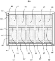
基板は図5に示すように、ガラスなどの透明基板41上にSiO2膜および/あるいはSiN膜からなる絶縁膜が形成された上にゲート電極がパターニングされた後、ゲート絶縁膜および非晶質シリコン膜42が形成されている。非晶質シリコン膜厚は30〜150nmの範囲でTFT作成に使用されるが、ここでは非晶質シリコン膜厚50nmの場合について説明する。非晶質シリコン膜42はプラズマCVDなどの手法により成膜されるが、多量の水素が、典型的には8〜15原子%の濃度で含まれており、水素化非晶質シリコン膜とも称される。非晶質シリコン膜42は、まず450度、2時間程度の炉体アニールにより脱水素を行なう。この工程により、非晶質シリコン薄膜中の水素濃度は1原子%程度まで減少し、この後レーザ光を照射しても、急激な水素脱離によるシリコン膜の剥離、損傷が発生しない。この基板41は図1に示した装置のステージ12上に載置・固定される。
As shown in FIG. 5, the substrate is formed of an insulating film made of a SiO 2 film and / or a SiN film on a
まず、ゲート電極形成時に同時に形成された複数箇所のアライメントマーク43をCCDカメラ17で撮像して画像処理装置18で検出し、ステージ12の移動、あるいは座標の変換により、基板41の位置決めを行なう。アライメントマーク位置を基準に、設計座標に従って順次、所望の領域に連続発振レーザ光を照射する。図5において、画素領域44、および駆動回路領域54を破線で示しており、これらの領域にはゲート電極が形成されている。また、レーザ光はビーム整形器10により少なくとも一方向にトップフラットで矩形状のビームに整形される。たとえば、長手方向(走査方向と直交方向)が2mmの均一なエネルギ密度分布の、短手方向(走査方向)が0.1mmの均一なエネルギ密度分布のあるいは台形状のエネルギ密度分布あるいはガウス分布のビームに整形される。
First, a plurality of alignment marks 43 formed simultaneously with the formation of the gate electrode are picked up by the
基板が位置決めされた後、ステージ12が100mm/sの速度で走査を開始し、ビーム中心が画素領域44の1.5〜2mm程度手前の位置から連続発振レーザ光3の照射を開始する。画素領域45、46、47、48を通過した後、ビーム中心が1.5〜2mm程度過ぎた時点でレーザ照射を停止する。これにより、図6に示すように画素領域44、45、46、47、48の各一部分を含む領域50が微結晶化される。次いで、ステージ12をレーザ光の走査方向と直交する方向に2mm移動して、ステージ12を先ほどとは反対方向に移動することで、領域50’が微結晶化される。これを繰り返して、基板のうち、画素領域と駆動回路領域を含む領域が微結晶化される。この微結晶シリコン膜は溶融過程を経ていないため、非晶質シリコン膜と同程度の表面平坦度を有する。
After the substrate is positioned, the
必要な部分を微結晶化した後、必要に応じてビーム整形器10をビーム整形器20に切り替え、走査方向(短軸方向)が5μm、走査方向に直交する方向(長軸方向)に1mmの線状ビームに整形し、溶融再凝固を起こすに足りるパワー密度で短軸方向に500mm/sの走査速度で走査しつつ、各パネルに相当する駆動回路領域54、55、56、57、58に連続発振レーザ光をON/OFFしながら照射し、照射部分を溶融再結晶させることにより、結晶をレーザ光の走査方向に横方向成長させ、帯状多結晶膜に変換する。同様に、微結晶化領域50’についても駆動回路領域を帯状多結晶膜に変換する。これら、帯状多結晶膜の表面も凹凸が10nm程度の平坦な膜である。
After microcrystallizing necessary portions, the
上記手順により、図7に示すようにガラス基板41上に形成された非晶質シリコン薄膜42のうち、画素領域および駆動回路領域を含む領域60がレーザ照射により微結晶シリコン薄膜に変換される。更に必要に応じて、線状に整形されたレーザ光を照射しながら走査することで、図8に示すように、駆動回路領域54、54’、55、55’、56、56’、57、57’、58、58’のみが走査方向にラテラル成長した多結晶シリコン薄膜、即ち帯状多結晶シリコン薄膜に変換される。
By the above procedure, the
これらの工程の後、必要に応じて基板全面に非晶質シリコン膜が形成され、微結晶シリコン薄膜と非晶質シリコン膜、および帯状多結晶シリコン膜と非晶質シリコン膜の2層構造のシリコン膜はチャネル領域として所望の形状にパターニングされ、ソース・ドレイン電極を形成してそれぞれTFTが形成される。すなわち画素回路および駆動回路のトランジスタは微結晶シリコン膜と非晶質シリコン膜で、あるいは駆動回路のトランジスタのみは帯状多結晶シリコン膜と非晶質シリコン膜で構成された液晶表示装置が形成される。 After these steps, an amorphous silicon film is formed on the entire surface of the substrate as necessary, and has a two-layer structure of a microcrystalline silicon thin film and an amorphous silicon film, and a band-shaped polycrystalline silicon film and an amorphous silicon film. The silicon film is patterned into a desired shape as a channel region, and source / drain electrodes are formed to form TFTs. That is, a liquid crystal display device is formed in which the transistors of the pixel circuit and the drive circuit are formed of a microcrystalline silicon film and an amorphous silicon film, or only the transistors of the drive circuit are formed of a band-shaped polycrystalline silicon film and an amorphous silicon film. .
なお、図5〜図8においては、基板内を2行5列の10パネルで構成したが、基板の大きさおよびパネルの大きさにより数パネル〜数百パネルを製造することができる。また、図5〜図8においては、駆動回路をパネルの一辺に形成する構成としたが、必要に応じて、2辺に配置することも可能である。その場合には、必要に応じて基板を90度回転させてレーザを上述の走査と直交する方向に走査させ、所望の領域のみを帯状多結晶化を行なえばよい。 5 to 8, the inside of the substrate is composed of 10 panels of 2 rows and 5 columns, but several to hundreds of panels can be manufactured depending on the size of the substrate and the size of the panel. 5 to 8, the driving circuit is formed on one side of the panel. However, it can be arranged on two sides as necessary. In that case, if necessary, the substrate is rotated by 90 degrees, the laser is scanned in the direction orthogonal to the above-described scanning, and only a desired region is subjected to band-like polycrystallization.
レーザ照射による良好な微結晶化が可能な条件は、照射するレーザ光のパワー密度と照射時間で規定することができる。膜厚50nmの非晶質シリコン薄膜を対象とした実験の結果、図9に示す範囲で微結晶化が可能であった。即ち、図9において実線は微結晶化の下限を示し、実線より下の条件では結晶化ができない。一点鎖線は微結晶化の上限を示し、一点鎖線より上の条件では、結晶粒が大きく成長したり、シリコンが溶融して表面張力により凝集する。実線と一点鎖線で囲まれた条件範囲で、適正な微結晶化が実現できた。この条件では、シリコン膜は融点に近い温度まで上昇しているものの溶融にいたらず、固相状態で微結晶化したと推定される。ここで得られる微結晶は、結晶粒の大きさが100nm以下、典型的には30〜80nmと極めて小さく、表面はレーザ照射前と変化が見られない程度の平坦性を保っている。 Conditions under which fine microcrystallization can be achieved by laser irradiation can be defined by the power density and irradiation time of the laser beam to be irradiated. As a result of experiments on an amorphous silicon thin film having a thickness of 50 nm, microcrystallization was possible within the range shown in FIG. That is, in FIG. 9, the solid line indicates the lower limit of microcrystallization, and crystallization cannot be performed under conditions below the solid line. An alternate long and short dash line indicates the upper limit of microcrystallization. Under conditions above the alternate long and short dash line, crystal grains grow large, or silicon melts and aggregates due to surface tension. Appropriate microcrystallization was realized within the condition range surrounded by the solid line and the alternate long and short dash line. Under these conditions, it is estimated that the silicon film has risen to a temperature close to the melting point, but has not melted and has been microcrystallized in a solid state. The microcrystal obtained here has a crystal grain size of 100 nm or less, typically 30 to 80 nm, which is extremely small, and the surface is kept flat enough to show no change from that before laser irradiation.
図9から明らかなように、連続発振レーザ光の照射時間(任意の点に矩形のビームが到達してから通過し終わるまでの時間)が長いほど微結晶化のマージンが広い。ここで、微結晶化のマージンは微結晶のパワー密度上限をパワー密度下限で除した値で定義する。線状あるいは矩形状に整形したビームの走査方向に直行する方向の均一性および基板−投影レンズ間の変動に伴うパワー密度の変動が±10%、基板間および基板内の非晶質シリコン膜厚の変動に伴う、微結晶化に必要パワー密度の変動を±10%とすると、結晶化のマージンとして1.4以上が望ましい。その観点から、レーザの照射時間として、0.5ms以上、望ましくは1ms以上であれば、照射パワー密度の条件範囲が広く、十分に実用的なプロセスウインドウが確保できる。照射時間が0.1ms以下でも微結晶化が可能であるが、上述したようにレーザ出力の変動、パワー密度分布の不均一さ、更には非晶質シリコン膜の膜厚バラツキなどの影響を受けて、量産に適用できるほど、安定には形成できない。ここでのレーザの照射時間1msは、例えば走査方向に0.1mm幅に整形されたビームを100mm/sで走査することに相当する。走査方向に0.5mmに整形されたビームを照射した場合に、500mm/sで走査しても同じ結果が得られる。なお、一度微結晶化した領域に、同一条件で再度レーザを照射しても、変化は生じなかった。これは、レーザ波長について考察したとおり、微結晶化することで吸収係数が低下し、2度目の照射時には結晶成長が進むまでの温度上昇が生じないためである。また、先の走査領域と後の走査領域の重なり部においても、一度微結晶化した部分は再度照射されても変化しないため、ビームが重なった部分は重ならなかった部分と、ほとんど区別がつかない。このため、矩形ビームの長手方向の寸法が基板寸法より小さい場合に、複数回の走査で基板前面を照射しても、照射領域の重畳の有無にかかわらず、一様な微結晶が得られる。 As is clear from FIG. 9, the longer the irradiation time of the continuous wave laser beam (the time from the arrival of the rectangular beam at an arbitrary point to the end of passage) is, the wider the margin for microcrystallization is. Here, the margin for microcrystallization is defined by a value obtained by dividing the upper limit of power density of the microcrystal by the lower limit of power density. Uniformity in the direction perpendicular to the scanning direction of the beam shaped into a linear or rectangular shape and ± 10% variation in power density due to variation between the substrate and the projection lens, and amorphous silicon film thickness between and within the substrate Assuming that the fluctuation of the power density required for the microcrystallization due to the fluctuation is ± 10%, the crystallization margin is preferably 1.4 or more. From this point of view, if the laser irradiation time is 0.5 ms or longer, preferably 1 ms or longer, the condition range of the irradiation power density is wide and a sufficiently practical process window can be secured. Microcrystallization is possible even when the irradiation time is 0.1 ms or less. However, as described above, it is affected by fluctuations in laser output, nonuniformity in power density distribution, and variations in film thickness of the amorphous silicon film. Therefore, it cannot be formed so stably that it can be applied to mass production. The laser irradiation time of 1 ms here corresponds to, for example, scanning a beam shaped to a width of 0.1 mm in the scanning direction at 100 mm / s. When a beam shaped to 0.5 mm is irradiated in the scanning direction, the same result can be obtained even if scanning is performed at 500 mm / s. Note that even if the region once microcrystallized was irradiated again with laser under the same conditions, no change occurred. This is because, as discussed with respect to the laser wavelength, the absorption coefficient decreases by microcrystallization, and the temperature does not increase until the crystal growth proceeds at the second irradiation. In addition, even in the overlapping portion of the previous scanning region and the subsequent scanning region, the portion once microcrystallized does not change even when irradiated again, so that the portion where the beam overlaps can be almost distinguished from the portion where the beam does not overlap. Absent. For this reason, when the longitudinal dimension of the rectangular beam is smaller than the substrate dimension, even if the front surface of the substrate is irradiated by a plurality of scans, uniform microcrystals can be obtained regardless of whether or not the irradiation regions are superimposed.
次に、図11〜図14を用いて、レーザ光を非晶質シリコン薄膜に直接照射しつつ走査するに際し、既照射領域の状態をモニタし、レーザ光の出力を適正な範囲に制御することができることを説明する。 Next, when performing scanning while directly irradiating the amorphous silicon thin film with laser light using FIGS. 11 to 14, the state of the irradiated region is monitored and the output of the laser light is controlled within an appropriate range. Explain that you can.
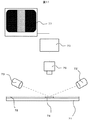
レーザ照射直後の結晶状態をモニタし、適正な結晶状態でない場合にレーザ条件を補正することで更に安定な微結晶膜に変換することができる。たとえば、図11に示す光学系を投影レンズ14の前後に設け、走査方向と逆側(既にレーザ光を照射した側)の光学系で結晶状態をモニタする。この光学系は浅い角度でレーザ照射領域を含む領域を照明する投光器73、73’と、基板表面を暗視野像として撮像するためのリニアセンサ75、画像処理装置76、表示装置77から構成されている。ガラス基板71上に形成された非晶質シリコン膜72とレーザ照射領域74を前記光学系で暗視野像として撮像すると、非晶質シリコン72表面はきわめて平坦であるため、リニアセンサ75には非晶質シリコン72表面からの散乱光が入射せず、明度は低い。また、照射したレーザ光のパワー密度が小さすぎて結晶化しない条件であれば、レーザ照射領域74の表面状態は非晶質シリコン72表面と同様であり、区別できない。その状態を図12(a)に示す。
By monitoring the crystal state immediately after laser irradiation and correcting the laser condition when the crystal state is not appropriate, it can be converted into a more stable microcrystalline film. For example, the optical system shown in FIG. 11 is provided before and after the
一方、微結晶化するに適正な条件でレーザ光を照射すると、図12(b)に示す様に、レーザ照射領域は微結晶化してわずかな散乱光が発生し、リニアセンサ75で非晶質シリコン72表面より若干明度が増加するが、十分に低い。しかい、レーザパワー密度が高過ぎる条件で照射すると、非晶質シリコン72は粒状結晶となりあるいは突起が形成されて散乱光が発生する。このため、図12(c)に示す様にレーザ照射領域74の明度が大きくなる。この場合、図12に示した閾値Aを越える明度が検出されるため、レーザ出力が高すぎる(パワー密度が大きすぎる)と判断して透過率可変フィルタでレーザ出力を低減する方向に調整する。
On the other hand, when laser light is irradiated under conditions suitable for microcrystallization, the laser irradiation region is microcrystallized and a slight amount of scattered light is generated as shown in FIG. Although the brightness is slightly higher than the surface of the
更に、図13に示す光学系を投影レンズ14の前後に設け、走査方向と逆側(既にレーザ光を照射した側)の光学系で結晶状態をモニタする。この光学系は非晶質シリコンと結晶質シリコンに対する吸収係数の差が大きい波長の光を照射する投光器81とレーザ照射領域を透過した光(1回透過光)を検出する光検出器82、あるいはガラス基板71を載置するステージ表面が白色アルミナあるいはジルコニアなどでコーティングされている場合には、シリコン膜表面での正反射を避けて、シリコン膜を2回透過したステージ表面からの反射・散乱光量を検出するための光検出器83から構成されている。光検出器82あるいは83からの出力は出力判定回路(図示せず)により設定した出力値と比較し、結晶状態が適正か否かを判定する。
Further, the optical system shown in FIG. 13 is provided in front of and behind the
図14に照射するレーザ出力とレーザ照射された領域の透過あるいは反射光の検出光量の関係を示す。レーザ照射前あるいは低出力の照射では非晶質シリコンのままであるため、投光器81からの光の透過光量は小さい。レーザ出力を増加させるに従い、非晶質シリコン膜は微結晶化し検出光量は増加する。更にレーザ出力を増加させ、粒状多結晶が形成されても検出光量の変化は小さく、ほぼ一定となる。このことから、一定となった検出光量を相対値1とした場合に、検出光量が0.9以下となった場合には結晶化が不十分、即ちレーザ出力が不足していると判断することができる。この結果を基に、レーザ出力が不足と判定された場合には、透過率連続波変フィルタの透過率を増加させることで、レーザ出力を調整する。
FIG. 14 shows the relationship between the laser output to be irradiated and the detected light amount of transmitted or reflected light in the laser irradiated region. Since the amorphous silicon remains before the laser irradiation or irradiation with low output, the amount of light transmitted from the
以上のとおり、レーザ照射領域の表面からの散乱光の大小によりレーザ出力が過大か否かを、レーザ照射領域を透過する光量の大小によりレーザ出力が過小か否かを判断することができ、これらの判断に従って非晶質シリコン膜に照射されるレーザ出力を調整することで、適正な微結晶膜への変換を高歩留まりで実現することができる。 As described above, it is possible to determine whether the laser output is excessive or not based on the size of scattered light from the surface of the laser irradiation region, and whether the laser output is excessive or not based on the amount of light transmitted through the laser irradiation region. By adjusting the laser output applied to the amorphous silicon film according to the above determination, conversion to an appropriate microcrystalline film can be realized with a high yield.
上記した方法により、所望の領域に安定に微結晶シリコンを得ることができた。この微結晶シリコン膜で形成したトランジスタは、いわゆるエキシマレーザアニールで形成した多結晶シリコン膜から形成したトランジスタと比べて、移動度では劣るものの、特性バラツキが小さく、またガラス基板上におけるトランジスタ特性の方向依存性もない。 By the above method, microcrystalline silicon could be stably obtained in a desired region. The transistor formed of this microcrystalline silicon film has less mobility than a transistor formed from a polycrystalline silicon film formed by so-called excimer laser annealing, but has less characteristic variation, and the direction of transistor characteristics on a glass substrate There is no dependency.
次に、本発明である平面表示装置の製造方法を実施するに好適な別な平面表示装置を製造する装置の光学系構成を図10に示す。筐体101に納められた複数のLDで発光したレーザ光はそれぞれ光ファイバ102、102’、102”・・・を介してカライドスコープ103に入射する。入射した各々のレーザ光はカライドスコープ103内で混合され、レーザ光104として安全シャッタ105、結像レンズ106、矩形スリット107、投影レンズ108を透過して、XYステージ112上に載置された基板113上に縮小投影される。また、基板113上の観察あるいはアライメントマーク検出などを行なうためのダイクロイックミラー115、結像レンズ116、CCDカメラ117、画像処理装置118を備え、制御装置114はLDのON/OFF、ステージ112の駆動、アライメントマークの検出などを制御する。
Next, FIG. 10 shows an optical system configuration of an apparatus for manufacturing another flat display device suitable for carrying out the flat display device manufacturing method according to the present invention. Laser beams emitted from a plurality of LDs housed in the
まず照射するレーザ光の波長について考える。図2に非晶質シリコンと結晶シリコンの分光吸収係数(α)を示す。横軸は波長(nm)、縦軸は吸収係数α(cm−1)である。非晶質シリコン膜を微結晶化するには非晶質シリコン薄膜に対して吸収のある波長を照射する必要がある。しかし、吸収係数が大きすぎるとレーザ光は非晶質シリコン膜を透過できずに表面のみ加熱される。当然、熱伝導により基板と接する側まで加熱されるが、表面とは温度が異なり結晶化の状態も異なるため、好ましくない。即ち、レーザ光の浸透深さ(吸収係数の逆数)が非晶質シリコン膜の膜厚程度以上であることが望ましい。例えば非晶質シリコン膜の膜厚を40nmとすると、浸透深さが40nm程度以上(=吸収係数が2.5×10^5(cm−1)以下)が望ましく、図2からこの値は波長に換算すると445nm以上に相当する。シリコンの吸収係数はシリコン中の不純物濃度あるいは欠陥密度などによって変動するが、おおむね440nm以上と考えることができる。非晶質シリコン膜の膜厚が大きい場合には、より長波長側にシフトし、たとえば非晶質シリコン膜厚が100nmの場合には、おおむね520nm以上である。 First, consider the wavelength of the laser beam to be irradiated. FIG. 2 shows the spectral absorption coefficient (α) of amorphous silicon and crystalline silicon. The horizontal axis represents wavelength (nm), and the vertical axis represents absorption coefficient α (cm −1 ). In order to microcrystallize the amorphous silicon film, it is necessary to irradiate the amorphous silicon thin film with an absorbing wavelength. However, if the absorption coefficient is too large, the laser beam cannot be transmitted through the amorphous silicon film and only the surface is heated. Of course, it is heated to the side in contact with the substrate by heat conduction, but it is not preferable because the temperature is different from the surface and the crystallization state is also different. That is, it is desirable that the penetration depth of laser light (the reciprocal of the absorption coefficient) be equal to or greater than the film thickness of the amorphous silicon film. For example, if the film thickness of the amorphous silicon film is 40 nm, the penetration depth is preferably about 40 nm or more (= absorption coefficient is 2.5 × 10 ^ 5 (cm −1 ) or less). Is equivalent to 445 nm or more. The absorption coefficient of silicon varies depending on the impurity concentration or defect density in the silicon, but can be considered to be approximately 440 nm or more. When the film thickness of the amorphous silicon film is large, it shifts to a longer wavelength side. For example, when the film thickness of the amorphous silicon film is 100 nm, it is approximately 520 nm or more.
一方、非晶質シリコン膜にレーザ光を照射して微結晶化したときに、吸収係数が増大するのは望ましくない。即ち、適正な条件でレーザを照射して非晶質シリコン膜を微結晶化した瞬間に吸収係数が増大し、微結晶膜が溶融したり、結晶粒が大きく成長したりして、微結晶膜が形成できない。逆に適正な条件でレーザを照射して非晶質シリコン膜を微結晶化した瞬間に吸収係数が減少すると、微結晶膜が保存される。その観点から、照射するレーザ光の波長に対する非晶質シリコンの吸収係数が、結晶シリコンの吸収係数より大きい必要がある。この吸収係数が逆転する波長はシリコン膜の製造プロセス・不純物濃度・欠陥密度により異なるが、650〜750nmの範囲にあり、図2の場合には670nmに相当する。この波長より短い波長のレーザ光を照射する必要はある。この波長はシリコン膜の膜厚には依存しない。 On the other hand, it is not desirable that the absorption coefficient increases when the amorphous silicon film is irradiated with laser light to be microcrystallized. That is, the absorption coefficient increases at the moment when the amorphous silicon film is microcrystallized by irradiating a laser under appropriate conditions, and the microcrystal film melts or crystal grains grow greatly, Cannot be formed. On the other hand, if the absorption coefficient decreases at the moment when the amorphous silicon film is microcrystallized by irradiating a laser under appropriate conditions, the microcrystalline film is preserved. From this viewpoint, the absorption coefficient of amorphous silicon with respect to the wavelength of the laser beam to be irradiated needs to be larger than the absorption coefficient of crystalline silicon. The wavelength at which the absorption coefficient is reversed varies depending on the manufacturing process, impurity concentration, and defect density of the silicon film, but is in the range of 650 to 750 nm, and corresponds to 670 nm in the case of FIG. It is necessary to irradiate laser light having a wavelength shorter than this wavelength. This wavelength does not depend on the film thickness of the silicon film.
以上のことから、本発明に適用するレーザ光の波長としては、概ね750nm以下である必要があり、445〜670nmがより望ましい。本実施例の説明では発振波長が670nmのLDを使用した場合について説明する。 From the above, the wavelength of the laser light applied to the present invention needs to be approximately 750 nm or less, and more preferably 445 to 670 nm. In the description of this embodiment, a case where an LD having an oscillation wavelength of 670 nm is used will be described.
複数のLDから出射したレーザ光104は、ファイバ102により伝送されてカライドスコープ103に入射される。入射されたレーザ光はカライドスコープ103内で多重反射しながら混合され、出口でのエネルギ密度が均一化される。また、カライドスコープ103の光軸に垂直な断面形状は連続的に変化し、最終的に基板上に照射されるビームの形状になる。出口の大きさは、投影光学系の倍率に依存する。材質としてはレーザ光104に対して透明な材質、例えば石英などで形成されてもよいし、レーザ光104に対して高反射率の内面を有する中空構造でも良い。出口の形状を1辺が20mm×1mmの矩形とすると、結像レンズ106で等倍(1倍)でスリット107面上に投影し、更にスリット像を投影レンズ108で基板113上に1/10に縮小投影することで、照射領域を2mm×0.1mmの矩形状とすることができ、図1に示した光学系によるものと同一の微結晶化を行なうことができる。
次に、各部の動作・機能について詳細に説明する。LDとしては発振波長670nm、発振出力5Wの赤色半導体レーザを使用することができる。10個のLD出力を各々ファイバでカライドスコープ103内に入力することにより、総合出力として50Wが得られる。更に出力が必要な場合には、LDを増設すればよい。レーザ光のON/OFFはLDを直接制御して行なう。
Next, the operation and function of each unit will be described in detail. As the LD, a red semiconductor laser having an oscillation wavelength of 670 nm and an oscillation output of 5 W can be used. By inputting the 10 LD outputs into the
レーザ光は通常はシャッタ105で遮られており、レーザ光を照射する場合のみ、このシャッタ105を開く(ON状態にする)ことで、レーザ光を出力させる。このほか、安全上の観点から緊急にレーザ光の照射を停止したい場合にも、シャッタ105を閉じればよい。 The laser beam is normally blocked by the shutter 105, and only when the laser beam is irradiated, the laser beam is output by opening (turning on) the shutter 105. In addition, the shutter 105 may be closed when it is urgently desired to stop the laser beam irradiation from the viewpoint of safety.
シャッタ105を通過したレーザ光は結像レンズ106により矩形スリット107上に、例えば1対1で投影される。これにより、矩形スリット107上ではカライドスコープ103出口でのパワー密度分布が保存される。必要に応じて矩形スリット107で所望の長手方向寸法に調整し、透過するビームとしてほぼ均一で所望の寸法を有する、パワー密度分布が均一なビームを得る。このビームを投影レンズ108で、基板113上に1/10に縮小投影する。なお、ここでは結像レンズ106を1/1、投影レンズ108を1/10とし、総合で1/10に縮小投影する説明をしたが、必要に応じて倍率を変更しても差し支えない。基板上で必要とする寸法とカライドスコープ103出口の寸法に応じて、倍率を選択すればよい。
The laser light that has passed through the shutter 105 is projected onto the
以下に、図10に構成を示した製造装置を用いた平面表示装置の製造方法の実施例2について、図に従い詳細に説明する。ここでもボトムゲート構造を対象とした場合について説明するが、トップゲート構造の場合も基本的には同様の工程で製造することができる。 Hereinafter, a second embodiment of the method for manufacturing a flat display device using the manufacturing apparatus having the configuration shown in FIG. 10 will be described in detail with reference to the drawings. Here, the case where the bottom gate structure is used will be described. However, the top gate structure can also be basically manufactured by the same process.
基板は図5に示すように、ガラスなどの透明基板41上にSiO2膜および/あるいはSiN膜からなる絶縁膜が形成された上にゲート電極がパターニングされた後、ゲート絶縁膜および非晶質シリコン膜42が形成されている。非晶質シリコン膜はプラズマCVDなどの手法により成膜されるが、多量の水素が、典型的には8〜15原子%の濃度で含まれており、水素化非晶質シリコン膜とも称される。非晶質シリコン膜厚は30〜150nmの範囲でTFT作成に使用されるが、ここでは非晶質シリコン膜厚50nmの場合について説明する。この基板41はあらかじめ炉体アニールにより、450℃、2時間の処理により脱水素処理を行い、図10に示した装置のステージ112上に載置・固定される。
As shown in FIG. 5, the substrate is formed of an insulating film made of a SiO 2 film and / or a SiN film on a
まず、ゲート電極形成時に同時に形成された複数箇所のアライメントマーク43をCCDカメラ117で撮像して画像処理装置118で検出し、ステージ112の移動、あるいは座標の変換により、基板41の位置決めを行なう。アライメントマーク位置を基準に設計座標に従い、順次、所望の領域の微結晶化を行なう。図5において、画素領域44、および駆動回路領域54を破線で示しており、これらの領域にはゲート電極が形成されている。レーザ光はカライドスコープ103によりトップフラットで矩形状のビームに整形される。たとえば、長手方向(走査方向と直交方向)が2mmの均一なエネルギ密度分布の、短手方向(走査方向)が0.1mmの均一なエネルギ密度分布のあるいは台形状あるいはガウス分布のエネルギ密度分布のビームに整形される。
First, a plurality of alignment marks 43 formed simultaneously with the formation of the gate electrode are picked up by the
基板が位置決めされた後、ステージ12が100mm/sの速度で走査を開始し、ビーム中心が画素領域44の1.5〜2mm程度手前の位置から連続発振レーザ光3の照射を開始する。画素領域45、46、47、48を通過した後、ビーム中心が1.5〜2mm程度過ぎた時点でレーザ照射を停止する。これにより、図6に示すように画素領域44、45、46、47、48の各一部分を含む領域50が微結晶化される。次いで、ステージ12をレーザ光の走査方向と直交する方向に2mm移動して、ステージ112を先ほどとは反対方向に移動することで、領域50’が微結晶化される。これを繰り返して、基板全面のうち、画素領域と駆動回路領域を含む領域が微結晶化される。この微結晶シリコン膜は溶融過程を経ていないため、非晶質シリコン膜と同程度の表面平坦度を有する。なお、図10に示した装置では、連続発振レーザ光のON/OFFはLDを直接駆動することで行なう。
After the substrate is positioned, the
必要な部分を微結晶化した後、基板を搬出して次工程に進む。必要に応じて図10に示した装置により、走査方向(短軸方向)が5μm、走査方向に直交する方向(長軸方向)に1mmの線状ビームを、溶融再凝固を起こすに足りるパワー密度で短軸方向に500mm/sの走査速度で走査しつつ、各パネルに相当する駆動回路領域54、55、56、57、58に連続発振レーザ光をON/OFFしながら照射し、照射部分を溶融再結晶させることにより、結晶をレーザ光の走査方向に横方向成長させ、帯状多結晶膜に変換する。同様に、微結晶領域50’についても駆動回路領域を帯状多結晶膜に変換する。これら、帯状多結晶膜の表面も凹凸が10nm程度の平坦な膜である。
After the necessary portion is microcrystallized, the substrate is unloaded and proceeds to the next step. If necessary, the apparatus shown in FIG. 10 has a power density sufficient to cause melting and re-solidification of a linear beam of 5 μm in the scanning direction (short axis direction) and 1 mm in the direction orthogonal to the scanning direction (long axis direction). While driving at a scanning speed of 500 mm / s in the minor axis direction, the
上記手順により、図7に示すようにガラス基板41上に形成された非晶質シリコン薄膜42のうち、画素領域および駆動回路領域を含む領域60がレーザ照射により微結晶シリコン薄膜に変換される。更に必要に応じて、線状に整形されたレーザ光を照射しながら走査することで、図8に示すように、駆動回路領域54、54’、55、55’、56、56’、57、57’、58、58’のみが走査方向にラテラル成長した多結晶シリコン薄膜、即ち帯状多結晶シリコン薄膜に変換される。
By the above procedure, the
微結晶化工程の後、必要に応じて基板全面に非晶質シリコン膜が形成され、微結晶シリコン薄膜と非晶質シリコン膜、および帯状多結晶シリコン膜と非晶質シリコン膜の2層構造のシリコン膜は所望の形状にパターニングされ、ソース−ドレイン電極を形成してそれぞれTFTを形成することで、画素回路および駆動回路のトランジスタは微結晶シリコン膜と非晶質シリコン膜で、あるいは駆動回路のトランジスタのみは帯状多結晶シリコン膜と非晶質シリコン膜で構成された液晶表示装置が形成される。 After the microcrystallization process, an amorphous silicon film is formed on the entire surface of the substrate as necessary. A two-layer structure of a microcrystalline silicon thin film and an amorphous silicon film, and a band-shaped polycrystalline silicon film and an amorphous silicon film The silicon film is patterned into a desired shape, and the source-drain electrodes are formed to form TFTs, respectively, so that the transistors of the pixel circuit and the driving circuit are microcrystalline silicon film and amorphous silicon film, or the driving circuit A liquid crystal display device composed of a band-like polycrystalline silicon film and an amorphous silicon film is formed only with the transistor.
なお、図5〜図8においては、基板内を2行5列の10パネルで構成したが、基板の大きさおよびパネルの大きさにより数パネル〜数百パネルを製造することができる。また、図5〜図8においては、駆動回路をパネルの一辺に形成する構成としたが、必要に応じて、2辺に配置することも可能である。その場合には、必要に応じて基板を90度回転させてレーザを上述の走査と直交する方向に走査させ、所望の領域のみを帯状多結晶化を行なえばよい。 5 to 8, the inside of the substrate is composed of 10 panels of 2 rows and 5 columns, but several to hundreds of panels can be manufactured depending on the size of the substrate and the size of the panel. 5 to 8, the driving circuit is formed on one side of the panel. However, it can be arranged on two sides as necessary. In that case, if necessary, the substrate is rotated by 90 degrees, the laser is scanned in the direction orthogonal to the above-described scanning, and only a desired region is subjected to band-like polycrystallization.
図10に示した平面表示装置の製造装置では、LDの増設によりレーザ出力の増加が容易である。たとえば、出力5WのLDを100個設置することで発振器出力は500Wとなり、1走査で微結晶化できる幅が大きくできる。あるいは走査方向の幅を大きくすることで走査速度を上げることもできる。これにより、基板全面を微結晶化する場合でも、十分なスループットが得られる。 In the flat panel display manufacturing apparatus shown in FIG. 10, the laser output can be easily increased by adding LD. For example, by installing 100 LDs with an output of 5 W, the oscillator output becomes 500 W, and the width that can be crystallized in one scan can be increased. Alternatively, the scanning speed can be increased by increasing the width in the scanning direction. Thereby, even when the entire surface of the substrate is microcrystallized, a sufficient throughput can be obtained.
また、実施例1の説明で述べたように、非晶質シリコン膜にレーザ光を照射しつつ並行して既照射領域の表面粗さの程度、および非晶質シリコン膜と結晶質シリコン膜の吸収係数の差が大きい波長の光の透過度を検出することで結晶状態をモニタし、必要に応じて非晶質シリコン膜に照射されるレーザ出力を調整することで、高歩留まりに微結晶化を実現することができることは明らかである。なお、これらの内容について実施例1で詳細に説明したので、ここでは説明を省略する。 In addition, as described in the description of the first embodiment, the surface roughness of the already irradiated region is irradiated while the amorphous silicon film is irradiated with the laser beam, and the amorphous silicon film and the crystalline silicon film. The crystal state is monitored by detecting the transmittance of light with a wavelength with a large difference in absorption coefficient, and the laser output irradiated to the amorphous silicon film is adjusted as necessary to achieve fine crystallization. It is clear that can be realized. In addition, since these contents were demonstrated in detail in Example 1, description is abbreviate | omitted here.
上記した実施例の説明から明らかなように、本発明の趣旨は余分な工程を追加することなく、非晶質シリコン膜に直接連続発振レーザ光を照射することにより微結晶化を行なう方法を提供するものである。これにより、微結晶膜で形成したトランジスタは特性のバラツキが小さく、また基板内でのソース−ドレイン方向に依存しない特性のトランジスタが得られ、これらのトランジスタで構成された平面表示装置を製造することができる。 As is apparent from the above description of the embodiments, the gist of the present invention is to provide a method for performing microcrystallization by directly irradiating an amorphous silicon film with continuous wave laser light without adding an extra step. To do. As a result, a transistor formed of a microcrystalline film has a small variation in characteristics, and a transistor having characteristics independent of the source-drain direction in the substrate can be obtained, and a flat display device including these transistors is manufactured. Can do.
本発明の平面表示装置の製造方法は、液晶表示装置あるいは有機EL表示装置などの平面表示装置の製造に適用することができる。 The method for producing a flat display device of the present invention can be applied to the production of a flat display device such as a liquid crystal display device or an organic EL display device.
1…レーザダイオード、2…光ファイバ、3…レーザ光、4…レーザ発振器、6…透過率連続可変NDフィルタ、7…変調器、9…ビーム径調整器、10…ビーム整形器、12…ステージ、13…基板、14…投影レンズ、17…CCDカメラ、18…画像処理装置、19…制御装置、33…非晶質シリコン薄膜、34…微結晶シリコン薄膜、43…アライメントマーク、44…画素領域、45、46、47、48、49…駆動回路領域、50、60…微結晶化領域、73、81…投光器、75…リニアセンサ、76…画像処理装置、77…表示装置、82、83…光検出器、101…筐体、102…光ファイバ、103…カライドスコープ、105…シャッタ、114…制御装置、117…CCDカメラ
DESCRIPTION OF
Claims (13)
前記工程が、レーザ源から発振されたレーザ光を、線状または矩形状で少なくとも一方向に均一なエネルギ分布を有するビームに変換するための均一化光学系に入力し、均一なエネルギ分布に変換されたレーザ光を前記非晶質シリコン薄膜の表面に直接照射しつつ、前記一方向と直交方向にレーザ光を相対的に走査して、前記非晶質シリコン薄膜を、結晶粒径が100nm以下の微結晶シリコン薄膜に変換することを特徴とする平面表示装置の製造方法。 A method of manufacturing a flat panel display device including a step of irradiating an amorphous silicon thin film formed on an insulating substrate with a laser beam to convert it into a microcrystalline silicon thin film,
The above process inputs the laser beam oscillated from the laser source into a linear or rectangular beam having a uniform energy distribution in at least one direction and converts it into a uniform energy distribution. While directly irradiating the surface of the amorphous silicon thin film with the laser beam, the laser beam is scanned relatively in the direction orthogonal to the one direction, so that the amorphous silicon thin film has a crystal grain size of 100 nm or less. A method for manufacturing a flat display device, characterized by converting to a microcrystalline silicon thin film.
Priority Applications (1)
| Application Number | Priority Date | Filing Date | Title |
|---|---|---|---|
| JP2008222063A JP2010056433A (en) | 2008-08-29 | 2008-08-29 | Method of manufacturing flat panel display device |
Applications Claiming Priority (1)
| Application Number | Priority Date | Filing Date | Title |
|---|---|---|---|
| JP2008222063A JP2010056433A (en) | 2008-08-29 | 2008-08-29 | Method of manufacturing flat panel display device |
Publications (1)
| Publication Number | Publication Date |
|---|---|
| JP2010056433A true JP2010056433A (en) | 2010-03-11 |
Family
ID=42072007
Family Applications (1)
| Application Number | Title | Priority Date | Filing Date |
|---|---|---|---|
| JP2008222063A Pending JP2010056433A (en) | 2008-08-29 | 2008-08-29 | Method of manufacturing flat panel display device |
Country Status (1)
| Country | Link |
|---|---|
| JP (1) | JP2010056433A (en) |
Cited By (1)
| Publication number | Priority date | Publication date | Assignee | Title |
|---|---|---|---|---|
| WO2012060104A1 (en) * | 2010-11-02 | 2012-05-10 | パナソニック株式会社 | Method for manufacturing transistor, transistor, and display device |
Citations (6)
| Publication number | Priority date | Publication date | Assignee | Title |
|---|---|---|---|---|
| JP2001308009A (en) * | 2000-02-15 | 2001-11-02 | Matsushita Electric Ind Co Ltd | Non-single crystal film, substrate therewith method and device for manufacturing the same, inspection device and method of inspecting the same, thin-film transistor formed by use thereof, thin-film transistor array and image display device |
| JP2002008976A (en) * | 2000-06-20 | 2002-01-11 | Mitsubishi Electric Corp | Method and equipment of manufacturing semiconductor device |
| JP2004228486A (en) * | 2003-01-27 | 2004-08-12 | Mitsubishi Electric Corp | Laser annealing device |
| JP2005099427A (en) * | 2003-09-25 | 2005-04-14 | Hitachi Ltd | Display panel manufacturing method and display panel |
| JP2006261634A (en) * | 2005-02-17 | 2006-09-28 | Mitsubishi Electric Corp | Semiconductor device and manufacturing method thereof |
| JP2007115841A (en) * | 2005-10-19 | 2007-05-10 | Japan Steel Works Ltd:The | Crystallization method of thin film material and its device |
-
2008
- 2008-08-29 JP JP2008222063A patent/JP2010056433A/en active Pending
Patent Citations (6)
| Publication number | Priority date | Publication date | Assignee | Title |
|---|---|---|---|---|
| JP2001308009A (en) * | 2000-02-15 | 2001-11-02 | Matsushita Electric Ind Co Ltd | Non-single crystal film, substrate therewith method and device for manufacturing the same, inspection device and method of inspecting the same, thin-film transistor formed by use thereof, thin-film transistor array and image display device |
| JP2002008976A (en) * | 2000-06-20 | 2002-01-11 | Mitsubishi Electric Corp | Method and equipment of manufacturing semiconductor device |
| JP2004228486A (en) * | 2003-01-27 | 2004-08-12 | Mitsubishi Electric Corp | Laser annealing device |
| JP2005099427A (en) * | 2003-09-25 | 2005-04-14 | Hitachi Ltd | Display panel manufacturing method and display panel |
| JP2006261634A (en) * | 2005-02-17 | 2006-09-28 | Mitsubishi Electric Corp | Semiconductor device and manufacturing method thereof |
| JP2007115841A (en) * | 2005-10-19 | 2007-05-10 | Japan Steel Works Ltd:The | Crystallization method of thin film material and its device |
Cited By (1)
| Publication number | Priority date | Publication date | Assignee | Title |
|---|---|---|---|---|
| WO2012060104A1 (en) * | 2010-11-02 | 2012-05-10 | パナソニック株式会社 | Method for manufacturing transistor, transistor, and display device |
Similar Documents
| Publication | Publication Date | Title |
|---|---|---|
| JP4413569B2 (en) | Display panel manufacturing method and display panel | |
| JP3903761B2 (en) | Laser annealing method and laser annealing apparatus | |
| JP4474108B2 (en) | Display device, manufacturing method thereof, and manufacturing apparatus | |
| US7531390B2 (en) | Crystallizing method, thin-film transistor manufacturing method, thin-film transistor, and display device | |
| JP2010028128A (en) | Method of fablicating emiconductor device | |
| JP2005217209A (en) | Laser annealing method and laser annealer | |
| JP2005217210A (en) | Device for manufacturing flat panel display unit | |
| JP5085902B2 (en) | Manufacturing method of display device | |
| JP2008085236A (en) | Dual-wavelength laser annealing apparatus | |
| JP4674092B2 (en) | Manufacturing method of display device | |
| JP2009218524A (en) | Manufacturing method of flat display device, and flat display device | |
| US7723135B2 (en) | Manufacturing method of display device | |
| JP5126471B2 (en) | Method for manufacturing flat display device | |
| JP2011165717A (en) | Display device and method of manufacturing the same | |
| JP2007324519A (en) | Laser annealing device and method of manufacturing display device | |
| JP5214662B2 (en) | Method for producing polycrystalline silicon thin film | |
| JPH11121378A (en) | Manufacture of polycrystal semiconductor film, manufacture of semiconductor device, manufacture of liquid crystal display, and laser annealing device | |
| JP2010056433A (en) | Method of manufacturing flat panel display device | |
| JP4628879B2 (en) | Manufacturing method of display device | |
| JP2004039660A (en) | Method for manufacturing polycrystalline semiconductor film, method for manufacturing thin film transistor, display device, and pulse laser annealing apparatus | |
| KR100814821B1 (en) | Crystallization apparatus and method of silicon thin film | |
| JP2005276944A (en) | Semiconductor device, and device and method for manufacturing the same | |
| JP5179028B2 (en) | Display device manufacturing method and manufacturing apparatus thereof | |
| JP5068975B2 (en) | Laser annealing technology, semiconductor film, semiconductor device, and electro-optical device | |
| JPH06177033A (en) | Laser annealing |
Legal Events
| Date | Code | Title | Description |
|---|---|---|---|
| A621 | Written request for application examination |
Effective date: 20101215 Free format text: JAPANESE INTERMEDIATE CODE: A621 |
|
| A711 | Notification of change in applicant |
Free format text: JAPANESE INTERMEDIATE CODE: A712 Effective date: 20110218 |
|
| RD03 | Notification of appointment of power of attorney |
Free format text: JAPANESE INTERMEDIATE CODE: A7423 Effective date: 20110218 |
|
| A977 | Report on retrieval |
Free format text: JAPANESE INTERMEDIATE CODE: A971007 Effective date: 20130214 |
|
| A131 | Notification of reasons for refusal |
Free format text: JAPANESE INTERMEDIATE CODE: A131 Effective date: 20130219 |
|
| A02 | Decision of refusal |
Free format text: JAPANESE INTERMEDIATE CODE: A02 Effective date: 20130625 |