JP2010049269A - 干渉性変調 - Google Patents
干渉性変調 Download PDFInfo
- Publication number
- JP2010049269A JP2010049269A JP2009236776A JP2009236776A JP2010049269A JP 2010049269 A JP2010049269 A JP 2010049269A JP 2009236776 A JP2009236776 A JP 2009236776A JP 2009236776 A JP2009236776 A JP 2009236776A JP 2010049269 A JP2010049269 A JP 2010049269A
- Authority
- JP
- Japan
- Prior art keywords
- cavity
- display
- absorber
- reflector
- substrate
- Prior art date
- Legal status (The legal status is an assumption and is not a legal conclusion. Google has not performed a legal analysis and makes no representation as to the accuracy of the status listed.)
- Granted
Links
- 125000006850 spacer group Chemical group 0.000 claims abstract description 48
- 239000006096 absorbing agent Substances 0.000 claims abstract description 39
- 239000000758 substrate Substances 0.000 claims abstract description 36
- 238000000034 method Methods 0.000 claims abstract description 30
- 229920002120 photoresistant polymer Polymers 0.000 claims abstract description 11
- 230000003287 optical effect Effects 0.000 claims description 16
- 229910052751 metal Inorganic materials 0.000 claims description 12
- 239000002184 metal Substances 0.000 claims description 12
- 239000004065 semiconductor Substances 0.000 claims description 12
- 230000004044 response Effects 0.000 claims description 9
- 230000007246 mechanism Effects 0.000 claims description 7
- 230000001939 inductive effect Effects 0.000 claims description 3
- 239000011800 void material Substances 0.000 claims 1
- 238000005530 etching Methods 0.000 abstract description 8
- 230000008021 deposition Effects 0.000 abstract description 5
- 230000008569 process Effects 0.000 abstract description 2
- 230000003068 static effect Effects 0.000 abstract 1
- 239000000126 substance Substances 0.000 abstract 1
- 239000010408 film Substances 0.000 description 26
- 239000000463 material Substances 0.000 description 14
- 239000010409 thin film Substances 0.000 description 12
- 239000003086 colorant Substances 0.000 description 9
- 238000000926 separation method Methods 0.000 description 6
- 238000000151 deposition Methods 0.000 description 4
- CSCPPACGZOOCGX-UHFFFAOYSA-N Acetone Chemical compound CC(C)=O CSCPPACGZOOCGX-UHFFFAOYSA-N 0.000 description 2
- VYPSYNLAJGMNEJ-UHFFFAOYSA-N Silicium dioxide Chemical compound O=[Si]=O VYPSYNLAJGMNEJ-UHFFFAOYSA-N 0.000 description 2
- 238000010521 absorption reaction Methods 0.000 description 2
- 239000011521 glass Substances 0.000 description 2
- 230000006698 induction Effects 0.000 description 2
- 238000004519 manufacturing process Methods 0.000 description 2
- 239000002609 medium Substances 0.000 description 2
- 238000000059 patterning Methods 0.000 description 2
- 238000002310 reflectometry Methods 0.000 description 2
- BQCADISMDOOEFD-UHFFFAOYSA-N Silver Chemical compound [Ag] BQCADISMDOOEFD-UHFFFAOYSA-N 0.000 description 1
- MCMNRKCIXSYSNV-UHFFFAOYSA-N ZrO2 Inorganic materials O=[Zr]=O MCMNRKCIXSYSNV-UHFFFAOYSA-N 0.000 description 1
- 230000002421 anti-septic effect Effects 0.000 description 1
- 238000003491 array Methods 0.000 description 1
- 230000008859 change Effects 0.000 description 1
- 230000003247 decreasing effect Effects 0.000 description 1
- 238000010586 diagram Methods 0.000 description 1
- -1 dielectric Substances 0.000 description 1
- 230000000694 effects Effects 0.000 description 1
- 238000005566 electron beam evaporation Methods 0.000 description 1
- 239000012634 fragment Substances 0.000 description 1
- 238000007429 general method Methods 0.000 description 1
- 239000000976 ink Substances 0.000 description 1
- 230000031700 light absorption Effects 0.000 description 1
- 239000007788 liquid Substances 0.000 description 1
- 239000000203 mixture Substances 0.000 description 1
- RVTZCBVAJQQJTK-UHFFFAOYSA-N oxygen(2-);zirconium(4+) Chemical compound [O-2].[O-2].[Zr+4] RVTZCBVAJQQJTK-UHFFFAOYSA-N 0.000 description 1
- 238000001020 plasma etching Methods 0.000 description 1
- 230000003252 repetitive effect Effects 0.000 description 1
- 238000007493 shaping process Methods 0.000 description 1
- 235000012239 silicon dioxide Nutrition 0.000 description 1
- 239000000377 silicon dioxide Substances 0.000 description 1
- 229910052709 silver Inorganic materials 0.000 description 1
- 239000004332 silver Substances 0.000 description 1
- 239000002904 solvent Substances 0.000 description 1
- 238000009987 spinning Methods 0.000 description 1
- 238000004544 sputter deposition Methods 0.000 description 1
- 238000003756 stirring Methods 0.000 description 1
- 238000003860 storage Methods 0.000 description 1
- 229920003002 synthetic resin Polymers 0.000 description 1
- 239000000057 synthetic resin Substances 0.000 description 1
- 238000000427 thin-film deposition Methods 0.000 description 1
- WFKWXMTUELFFGS-UHFFFAOYSA-N tungsten Chemical compound [W] WFKWXMTUELFFGS-UHFFFAOYSA-N 0.000 description 1
- 229910052721 tungsten Inorganic materials 0.000 description 1
- 239000010937 tungsten Substances 0.000 description 1
- 238000002604 ultrasonography Methods 0.000 description 1
- 238000001429 visible spectrum Methods 0.000 description 1
- 238000003631 wet chemical etching Methods 0.000 description 1
Images


Classifications
-
- G—PHYSICS
- G02—OPTICS
- G02B—OPTICAL ELEMENTS, SYSTEMS OR APPARATUS
- G02B26/00—Optical devices or arrangements for the control of light using movable or deformable optical elements
- G02B26/001—Optical devices or arrangements for the control of light using movable or deformable optical elements based on interference in an adjustable optical cavity
-
- G—PHYSICS
- G02—OPTICS
- G02B—OPTICAL ELEMENTS, SYSTEMS OR APPARATUS
- G02B26/00—Optical devices or arrangements for the control of light using movable or deformable optical elements
- G02B26/02—Optical devices or arrangements for the control of light using movable or deformable optical elements for controlling the intensity of light
-
- G—PHYSICS
- G02—OPTICS
- G02B—OPTICAL ELEMENTS, SYSTEMS OR APPARATUS
- G02B26/00—Optical devices or arrangements for the control of light using movable or deformable optical elements
- G02B26/08—Optical devices or arrangements for the control of light using movable or deformable optical elements for controlling the direction of light
- G02B26/0816—Optical devices or arrangements for the control of light using movable or deformable optical elements for controlling the direction of light by means of one or more reflecting elements
- G02B26/0833—Optical devices or arrangements for the control of light using movable or deformable optical elements for controlling the direction of light by means of one or more reflecting elements the reflecting element being a micromechanical device, e.g. a MEMS mirror, DMD
- G02B26/0841—Optical devices or arrangements for the control of light using movable or deformable optical elements for controlling the direction of light by means of one or more reflecting elements the reflecting element being a micromechanical device, e.g. a MEMS mirror, DMD the reflecting element being moved or deformed by electrostatic means
-
- G—PHYSICS
- G02—OPTICS
- G02B—OPTICAL ELEMENTS, SYSTEMS OR APPARATUS
- G02B26/00—Optical devices or arrangements for the control of light using movable or deformable optical elements
- G02B26/08—Optical devices or arrangements for the control of light using movable or deformable optical elements for controlling the direction of light
- G02B26/0816—Optical devices or arrangements for the control of light using movable or deformable optical elements for controlling the direction of light by means of one or more reflecting elements
- G02B26/0833—Optical devices or arrangements for the control of light using movable or deformable optical elements for controlling the direction of light by means of one or more reflecting elements the reflecting element being a micromechanical device, e.g. a MEMS mirror, DMD
- G02B26/085—Optical devices or arrangements for the control of light using movable or deformable optical elements for controlling the direction of light by means of one or more reflecting elements the reflecting element being a micromechanical device, e.g. a MEMS mirror, DMD the reflecting means being moved or deformed by electromagnetic means
-
- G—PHYSICS
- G02—OPTICS
- G02B—OPTICAL ELEMENTS, SYSTEMS OR APPARATUS
- G02B26/00—Optical devices or arrangements for the control of light using movable or deformable optical elements
- G02B26/08—Optical devices or arrangements for the control of light using movable or deformable optical elements for controlling the direction of light
- G02B26/0816—Optical devices or arrangements for the control of light using movable or deformable optical elements for controlling the direction of light by means of one or more reflecting elements
- G02B26/0833—Optical devices or arrangements for the control of light using movable or deformable optical elements for controlling the direction of light by means of one or more reflecting elements the reflecting element being a micromechanical device, e.g. a MEMS mirror, DMD
- G02B26/0858—Optical devices or arrangements for the control of light using movable or deformable optical elements for controlling the direction of light by means of one or more reflecting elements the reflecting element being a micromechanical device, e.g. a MEMS mirror, DMD the reflecting means being moved or deformed by piezoelectric means
Landscapes
- Physics & Mathematics (AREA)
- General Physics & Mathematics (AREA)
- Optics & Photonics (AREA)
- Spectroscopy & Molecular Physics (AREA)
- Electromagnetism (AREA)
- Mechanical Light Control Or Optical Switches (AREA)
- Laminated Bodies (AREA)
Abstract
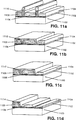
【解決手段】干渉性変調器空胴200、202は反射器208および誘導吸収体206を有する。干渉性変調器空胴200、202は各々の被着物によりさまざまな厚さの隣接スペーサーがリフトオフ技法によって、基質204上に構成される。または、単一の被着物(deposition)中に被着されたスペーサーの厚さをエッチングで選択的に削るためのエッチング処理が可能となるように、パターン成形がなされたフォトレジストを用いてもよい。組み合わされるパターンの干渉性変調器空胴200、202からフルカラー静止画像を形成することもできる。各空胴は反射器208および誘導吸収体206を含み、誘導吸収体206はその空胴に関連した1つの色を規定する1つの厚みを有するスペーサーを含む。
【選択図】図2
Description
親出願には、それらが光を変調させうるように、そのインピーダンス、すなわちアドミッタンスの逆数が能動的に調節されるような2種類の構造が記載されている。1つの方式は、空胴壁のうちの1つの静電的変形によってその光学的性質を変化させることができる変形可能な空胴である。誘電体、半導体または金属膜の層からなるこれらの壁の組成および厚さに応じて、印加電圧に対して異なる光応答(optical response)を示すさまざまな変調器の設計が可能となる。
このような設計の1つには、狭帯域フィルターおよび誘導吸収体(induced absorber)を有する混成フィルター(hybrid filter)として記載されるフィルターが含まれる。混成フィルターに付随する壁が反射器(reflector)と接触した場合には、一定範囲の入射光(incident light)が吸収される。これが起こるのは、誘導吸収体が、反射器のインピーダンスを、狭帯域フィルターを通過する範囲の周波数に関する入射媒体のそれと一致させるためである。
本発明は、一方が反射器であって他方が誘導吸収体である2つの壁を備えた空胴の間隔を静電的に変化させることによって光を変調させる。この空胴は、光学的に平滑な表面、すなわち干渉効果が発現するために十分な平滑さを有する表面上に構成される。
したがって、1つの局面において、本発明は一般に、反射器および誘導吸収体を有する干渉性変調器の空胴を特徴とする。
本発明のその他の利点および特徴は、以下の説明および請求の範囲から明らかになると思われる。
この両方の代替的な方法は、より大規模な方法の最終段階では、エッチングによって除去されてエアギャップが形成される防腐用スペーサー材料の、反復性被着およびパターン成形が含まれる。
例えば、スペーサー材料は最終的に除去される必要はなく、完成した装置の一部の代わりとして残っていてもよい。この様式では、以前に記載されたパターン成形技法をさらに用いることにより、単純な画素のアレイの代わりに任意のパターンを構成してもよい。このため、フルカラー静止画像を、従来の印刷法と類似した方法によって描画することもできる。従来の印刷では、画像は、提示されるさまざまに異なる色、すなわち赤色分解、青色分解、緑色分解および黒色分解という基本的には画像の単色像のサブセットである複数の色に分解される。フルカラー画像は、異なる色のインクを同一領域に用いてそれぞれの分離物を印刷することによって作成される。
Claims (45)
- 反射器および誘導吸収体を含む干渉性変調器空胴(interferometric modulator cavity)。
- 反射器が金属膜を含む、請求項1記載の空胴。
- 反射器が誘電体膜を含む、請求項1記載の空胴。
- 反射器が半導体膜を含む、請求項1記載の空胴。
- 反射器が、金属膜、誘電体膜および半導体膜のうち少なくとも2つの組み合わせを含む、請求項1記載の空胴。
- 誘導吸収体が2つの合致する層の間にサンドイッチ状に挟まれた吸収体を含む、請求項1記載の空胴。
- 合致する層のうち1つは入射媒体を備えた吸収体の境界部に位置し、他方の合致する層は反射器を備えた吸収体の境界部に位置している、請求項6記載の空胴。
- 合致する層のうち少なくとも1つが金属膜を含む、請求項6記載の空胴。
- 合致する層のうち少なくとも1つが誘導体膜を含む、請求項6記載の空胴。
- 合致する層のうち少なくとも1つが半導体膜を含む、請求項6記載の空胴。
- 合致する層のうち少なくとも1つが、金属膜、誘電体膜および半導体膜のうち少なくとも2つの組み合わせを含む、請求項6記載の空胴。
- 吸収体が金属などの高損失膜を含む、請求項6記載の空胴。
- 吸収体が半導体などの高損失膜を含む、請求項6記載の空胴。
- 吸収体が金属および半導体の膜の組み合わせを含む、請求項6記載の空胴。
- 1つの基板をさらに含む、請求項1記載の空胴。
- 基板が透明な入射媒体を含む、請求項15記載の空胴。
- 基板が不透明な媒体を含む、請求項15記載の空胴。
- 誘導吸収体が基板上に存在する、請求項15記載の空胴。
- 反射器が基板上に存在する、請求項15記載の空胴。
- 基板が反射器を含む、請求項15記載の空胴。
- 干渉性変調器のアレイを備えた直視型反射式平面パネルディスプレイ。
- アレイが、任意の特定の反射状態に調整するために配置された1組のアナログ式干渉性変調器を含む、請求項21記載のディスプレイ。
- アレイが、いくつかの組の干渉性変調器を含み、それぞれの組が複数の異なる対の反射状態を切り換えるために配置されている、請求項21記載のディスプレイ。
- 各々の変調器の輝度がパルス幅変調によって制御される、請求項21記載のディスプレイ。
- 各々の変調器画素の輝度が空間的ディザリングによって制御される、請求項21記載のディスプレイ。
- 各々の変調器の輝度がパルス幅変調および空間的ディザリングの組み合わせによって制御される、請求項21記載のディスプレイ。
- アレイがバックプレーンによって密閉されている、請求項21記載のディスプレイ。
- バックプレーンが一体型の要素を含む、請求項21記載のディスプレイ。
- バックプレーンが接着されている、請求項27記載のディスプレイ。
- バックプレーンが画素の電気機械的反応を改変させる電極を支持している、請求項27記載のディスプレイ。
- 各々の変調器が静電力によって作動される、請求項21記載のディスプレイ。
- 各々の変調器が圧電力によって作動される、請求項21記載のディスプレイ。
- 各々の変調器が磁力によって作動される、請求項21記載のディスプレイ。
- 映写システムで使用するための、請求項21記載のディスプレイ。
- 見る角度に応じて生じる色のずれを軽減または除去するために光学的補償機構が使用される、請求項21記載のディスプレイ。
- 補助的なフロントライティングを提供するために光学的補償機構が使用される、請求項21記載のディスプレイ。
- 見る角度に応じて生じる色のずれを軽減または除去するため、および補助的なフロントライティングを提供するために光学的補償機構が使用される、請求項21記載のディスプレイ。
- アレイが集積回路上に構成されている、請求項21記載のディスプレイ。
- アレイが電気回路に沿って基板上に構成されている、請求項21記載のディスプレイ。
- 各々の被着物によって異なる厚さのスペーサーが提供されるよう、別々に被着されたスペーサーのパターンを成形するためにリフトオフ(lift-off)技術が用いられる、基板上にさまざまな厚さの隣接スペーサーを構成するための方法。
- 単一の被着物中に被着されたスペーサーの厚さをエッチングで選択的に削るためのエッチング処理が行えるようにパターン成形がなされたフォトレジストの使用を含む、基板上にさまざまな厚さの隣接スペーサーを構成するための方法。
- 干渉性変調器空胴のアレイを含むフルカラー静止画像であって、各々の空胴が反射器および誘導吸収体を含み、該誘導吸収体が空胴に関連した色を規定するある厚みを有するスペーサーを含む、フルカラー静止画像。
- さまざまな空胴の輝度が空間的ディザリングによって決定される、請求項42記載の画像。
- 各々のパターンにおいてスペーサーがそのパターンに関連した1つの色を規定する1つの厚みを有し、すべてのパターンが組み合わされることによって画像が得られるような、別々のパターンのスペーサーまたはスペーサーを備えた干渉性変調器空胴を含むフルカラー静止画像。
- さまざまなパターンの輝度が空間的ディザリングによって決定される、請求項44記載の画像。
Applications Claiming Priority (2)
| Application Number | Priority Date | Filing Date | Title |
|---|---|---|---|
| US55463095A | 1995-11-06 | 1995-11-06 | |
| US08/554,630 | 1995-11-06 |
Related Parent Applications (1)
| Application Number | Title | Priority Date | Filing Date |
|---|---|---|---|
| JP51827697A Division JP4431196B2 (ja) | 1995-11-06 | 1996-11-06 | 干渉性変調 |
Publications (2)
| Publication Number | Publication Date |
|---|---|
| JP2010049269A true JP2010049269A (ja) | 2010-03-04 |
| JP4812869B2 JP4812869B2 (ja) | 2011-11-09 |
Family
ID=24214082
Family Applications (2)
| Application Number | Title | Priority Date | Filing Date |
|---|---|---|---|
| JP51827697A Expired - Fee Related JP4431196B2 (ja) | 1995-11-06 | 1996-11-06 | 干渉性変調 |
| JP2009236776A Expired - Fee Related JP4812869B2 (ja) | 1995-11-06 | 2009-10-14 | 干渉性変調 |
Family Applications Before (1)
| Application Number | Title | Priority Date | Filing Date |
|---|---|---|---|
| JP51827697A Expired - Fee Related JP4431196B2 (ja) | 1995-11-06 | 1996-11-06 | 干渉性変調 |
Country Status (2)
| Country | Link |
|---|---|
| JP (2) | JP4431196B2 (ja) |
| WO (1) | WO1997017628A1 (ja) |
Cited By (1)
| Publication number | Priority date | Publication date | Assignee | Title |
|---|---|---|---|---|
| JP2014534474A (ja) * | 2011-11-04 | 2014-12-18 | クォルコム・メムズ・テクノロジーズ・インコーポレーテッド | 電気機械システム反射型ディスプレイデバイスのための整合層薄膜 |
Families Citing this family (151)
| Publication number | Priority date | Publication date | Assignee | Title |
|---|---|---|---|---|
| US6674562B1 (en) | 1994-05-05 | 2004-01-06 | Iridigm Display Corporation | Interferometric modulation of radiation |
| US6680792B2 (en) | 1994-05-05 | 2004-01-20 | Iridigm Display Corporation | Interferometric modulation of radiation |
| US7138984B1 (en) | 2001-06-05 | 2006-11-21 | Idc, Llc | Directly laminated touch sensitive screen |
| US7550794B2 (en) | 2002-09-20 | 2009-06-23 | Idc, Llc | Micromechanical systems device comprising a displaceable electrode and a charge-trapping layer |
| US7123216B1 (en) | 1994-05-05 | 2006-10-17 | Idc, Llc | Photonic MEMS and structures |
| US20010003487A1 (en) | 1996-11-05 | 2001-06-14 | Mark W. Miles | Visible spectrum modulator arrays |
| US8014059B2 (en) * | 1994-05-05 | 2011-09-06 | Qualcomm Mems Technologies, Inc. | System and method for charge control in a MEMS device |
| US7460291B2 (en) | 1994-05-05 | 2008-12-02 | Idc, Llc | Separable modulator |
| US7297471B1 (en) | 2003-04-15 | 2007-11-20 | Idc, Llc | Method for manufacturing an array of interferometric modulators |
| US7907319B2 (en) | 1995-11-06 | 2011-03-15 | Qualcomm Mems Technologies, Inc. | Method and device for modulating light with optical compensation |
| US7471444B2 (en) | 1996-12-19 | 2008-12-30 | Idc, Llc | Interferometric modulation of radiation |
| KR100703140B1 (ko) | 1998-04-08 | 2007-04-05 | 이리다임 디스플레이 코포레이션 | 간섭 변조기 및 그 제조 방법 |
| US8928967B2 (en) | 1998-04-08 | 2015-01-06 | Qualcomm Mems Technologies, Inc. | Method and device for modulating light |
| WO2003007049A1 (en) | 1999-10-05 | 2003-01-23 | Iridigm Display Corporation | Photonic mems and structures |
| JP4830183B2 (ja) * | 2000-07-19 | 2011-12-07 | ソニー株式会社 | 光学多層構造体および光スイッチング素子、並びに画像表示装置 |
| US6589625B1 (en) | 2001-08-01 | 2003-07-08 | Iridigm Display Corporation | Hermetic seal and method to create the same |
| US6794119B2 (en) | 2002-02-12 | 2004-09-21 | Iridigm Display Corporation | Method for fabricating a structure for a microelectromechanical systems (MEMS) device |
| US6574033B1 (en) | 2002-02-27 | 2003-06-03 | Iridigm Display Corporation | Microelectromechanical systems device and method for fabricating same |
| US6741377B2 (en) * | 2002-07-02 | 2004-05-25 | Iridigm Display Corporation | Device having a light-absorbing mask and a method for fabricating same |
| TWI289708B (en) | 2002-12-25 | 2007-11-11 | Qualcomm Mems Technologies Inc | Optical interference type color display |
| JP2004219843A (ja) | 2003-01-16 | 2004-08-05 | Seiko Epson Corp | 光変調器、表示装置及びその製造方法 |
| TW200413810A (en) | 2003-01-29 | 2004-08-01 | Prime View Int Co Ltd | Light interference display panel and its manufacturing method |
| TW594360B (en) | 2003-04-21 | 2004-06-21 | Prime View Int Corp Ltd | A method for fabricating an interference display cell |
| US7221495B2 (en) | 2003-06-24 | 2007-05-22 | Idc Llc | Thin film precursor stack for MEMS manufacturing |
| TWI231865B (en) | 2003-08-26 | 2005-05-01 | Prime View Int Co Ltd | An interference display cell and fabrication method thereof |
| JP3979982B2 (ja) | 2003-08-29 | 2007-09-19 | シャープ株式会社 | 干渉性変調器および表示装置 |
| TW593126B (en) | 2003-09-30 | 2004-06-21 | Prime View Int Co Ltd | A structure of a micro electro mechanical system and manufacturing the same |
| US7012726B1 (en) | 2003-11-03 | 2006-03-14 | Idc, Llc | MEMS devices with unreleased thin film components |
| US7161728B2 (en) | 2003-12-09 | 2007-01-09 | Idc, Llc | Area array modulation and lead reduction in interferometric modulators |
| US7142346B2 (en) | 2003-12-09 | 2006-11-28 | Idc, Llc | System and method for addressing a MEMS display |
| US7342705B2 (en) | 2004-02-03 | 2008-03-11 | Idc, Llc | Spatial light modulator with integrated optical compensation structure |
| US7532194B2 (en) | 2004-02-03 | 2009-05-12 | Idc, Llc | Driver voltage adjuster |
| US7119945B2 (en) | 2004-03-03 | 2006-10-10 | Idc, Llc | Altering temporal response of microelectromechanical elements |
| US7855824B2 (en) | 2004-03-06 | 2010-12-21 | Qualcomm Mems Technologies, Inc. | Method and system for color optimization in a display |
| US7476327B2 (en) | 2004-05-04 | 2009-01-13 | Idc, Llc | Method of manufacture for microelectromechanical devices |
| US7060895B2 (en) | 2004-05-04 | 2006-06-13 | Idc, Llc | Modifying the electro-mechanical behavior of devices |
| US7164520B2 (en) | 2004-05-12 | 2007-01-16 | Idc, Llc | Packaging for an interferometric modulator |
| US7256922B2 (en) | 2004-07-02 | 2007-08-14 | Idc, Llc | Interferometric modulators with thin film transistors |
| EP1855142A3 (en) | 2004-07-29 | 2008-07-30 | Idc, Llc | System and method for micro-electromechanical operating of an interferometric modulator |
| US7560299B2 (en) | 2004-08-27 | 2009-07-14 | Idc, Llc | Systems and methods of actuating MEMS display elements |
| US7551159B2 (en) | 2004-08-27 | 2009-06-23 | Idc, Llc | System and method of sensing actuation and release voltages of an interferometric modulator |
| US7499208B2 (en) | 2004-08-27 | 2009-03-03 | Udc, Llc | Current mode display driver circuit realization feature |
| US7515147B2 (en) | 2004-08-27 | 2009-04-07 | Idc, Llc | Staggered column drive circuit systems and methods |
| US7602375B2 (en) | 2004-09-27 | 2009-10-13 | Idc, Llc | Method and system for writing data to MEMS display elements |
| US8878825B2 (en) | 2004-09-27 | 2014-11-04 | Qualcomm Mems Technologies, Inc. | System and method for providing a variable refresh rate of an interferometric modulator display |
| US7532195B2 (en) | 2004-09-27 | 2009-05-12 | Idc, Llc | Method and system for reducing power consumption in a display |
| BRPI0515883A (pt) * | 2004-09-27 | 2008-08-12 | Idc Llc | método e dispositivo para manipular cor em um display |
| US7355780B2 (en) | 2004-09-27 | 2008-04-08 | Idc, Llc | System and method of illuminating interferometric modulators using backlighting |
| US7415186B2 (en) | 2004-09-27 | 2008-08-19 | Idc, Llc | Methods for visually inspecting interferometric modulators for defects |
| US7289259B2 (en) | 2004-09-27 | 2007-10-30 | Idc, Llc | Conductive bus structure for interferometric modulator array |
| US7911428B2 (en) * | 2004-09-27 | 2011-03-22 | Qualcomm Mems Technologies, Inc. | Method and device for manipulating color in a display |
| US7460246B2 (en) | 2004-09-27 | 2008-12-02 | Idc, Llc | Method and system for sensing light using interferometric elements |
| US7630119B2 (en) | 2004-09-27 | 2009-12-08 | Qualcomm Mems Technologies, Inc. | Apparatus and method for reducing slippage between structures in an interferometric modulator |
| US7349136B2 (en) | 2004-09-27 | 2008-03-25 | Idc, Llc | Method and device for a display having transparent components integrated therein |
| US8102407B2 (en) | 2004-09-27 | 2012-01-24 | Qualcomm Mems Technologies, Inc. | Method and device for manipulating color in a display |
| US7161730B2 (en) | 2004-09-27 | 2007-01-09 | Idc, Llc | System and method for providing thermal compensation for an interferometric modulator display |
| US7453579B2 (en) | 2004-09-27 | 2008-11-18 | Idc, Llc | Measurement of the dynamic characteristics of interferometric modulators |
| US7554714B2 (en) | 2004-09-27 | 2009-06-30 | Idc, Llc | Device and method for manipulation of thermal response in a modulator |
| US7807488B2 (en) | 2004-09-27 | 2010-10-05 | Qualcomm Mems Technologies, Inc. | Display element having filter material diffused in a substrate of the display element |
| US7136213B2 (en) | 2004-09-27 | 2006-11-14 | Idc, Llc | Interferometric modulators having charge persistence |
| US7349141B2 (en) | 2004-09-27 | 2008-03-25 | Idc, Llc | Method and post structures for interferometric modulation |
| US7372613B2 (en) | 2004-09-27 | 2008-05-13 | Idc, Llc | Method and device for multistate interferometric light modulation |
| US7343080B2 (en) | 2004-09-27 | 2008-03-11 | Idc, Llc | System and method of testing humidity in a sealed MEMS device |
| US7535466B2 (en) | 2004-09-27 | 2009-05-19 | Idc, Llc | System with server based control of client device display features |
| US7310179B2 (en) | 2004-09-27 | 2007-12-18 | Idc, Llc | Method and device for selective adjustment of hysteresis window |
| US7545550B2 (en) | 2004-09-27 | 2009-06-09 | Idc, Llc | Systems and methods of actuating MEMS display elements |
| US7446927B2 (en) | 2004-09-27 | 2008-11-04 | Idc, Llc | MEMS switch with set and latch electrodes |
| US20060077148A1 (en) * | 2004-09-27 | 2006-04-13 | Gally Brian J | Method and device for manipulating color in a display |
| US7420725B2 (en) | 2004-09-27 | 2008-09-02 | Idc, Llc | Device having a conductive light absorbing mask and method for fabricating same |
| US8031133B2 (en) | 2004-09-27 | 2011-10-04 | Qualcomm Mems Technologies, Inc. | Method and device for manipulating color in a display |
| US7130104B2 (en) | 2004-09-27 | 2006-10-31 | Idc, Llc | Methods and devices for inhibiting tilting of a mirror in an interferometric modulator |
| US7527995B2 (en) | 2004-09-27 | 2009-05-05 | Qualcomm Mems Technologies, Inc. | Method of making prestructure for MEMS systems |
| US7405861B2 (en) | 2004-09-27 | 2008-07-29 | Idc, Llc | Method and device for protecting interferometric modulators from electrostatic discharge |
| US7626581B2 (en) | 2004-09-27 | 2009-12-01 | Idc, Llc | Device and method for display memory using manipulation of mechanical response |
| US7417735B2 (en) | 2004-09-27 | 2008-08-26 | Idc, Llc | Systems and methods for measuring color and contrast in specular reflective devices |
| US8362987B2 (en) | 2004-09-27 | 2013-01-29 | Qualcomm Mems Technologies, Inc. | Method and device for manipulating color in a display |
| US7359066B2 (en) | 2004-09-27 | 2008-04-15 | Idc, Llc | Electro-optical measurement of hysteresis in interferometric modulators |
| US7710632B2 (en) * | 2004-09-27 | 2010-05-04 | Qualcomm Mems Technologies, Inc. | Display device having an array of spatial light modulators with integrated color filters |
| US7564612B2 (en) | 2004-09-27 | 2009-07-21 | Idc, Llc | Photonic MEMS and structures |
| US7653371B2 (en) * | 2004-09-27 | 2010-01-26 | Qualcomm Mems Technologies, Inc. | Selectable capacitance circuit |
| US7420728B2 (en) | 2004-09-27 | 2008-09-02 | Idc, Llc | Methods of fabricating interferometric modulators by selectively removing a material |
| US7304784B2 (en) | 2004-09-27 | 2007-12-04 | Idc, Llc | Reflective display device having viewable display on both sides |
| US7928928B2 (en) | 2004-09-27 | 2011-04-19 | Qualcomm Mems Technologies, Inc. | Apparatus and method for reducing perceived color shift |
| AU2005289996A1 (en) * | 2004-09-27 | 2006-04-06 | Idc, Llc | Reduced capacitance display element |
| US7302157B2 (en) | 2004-09-27 | 2007-11-27 | Idc, Llc | System and method for multi-level brightness in interferometric modulation |
| US7373026B2 (en) | 2004-09-27 | 2008-05-13 | Idc, Llc | MEMS device fabricated on a pre-patterned substrate |
| US7525730B2 (en) | 2004-09-27 | 2009-04-28 | Idc, Llc | Method and device for generating white in an interferometric modulator display |
| US7405924B2 (en) | 2004-09-27 | 2008-07-29 | Idc, Llc | System and method for protecting microelectromechanical systems array using structurally reinforced back-plate |
| US20060176487A1 (en) | 2004-09-27 | 2006-08-10 | William Cummings | Process control monitors for interferometric modulators |
| US8004504B2 (en) | 2004-09-27 | 2011-08-23 | Qualcomm Mems Technologies, Inc. | Reduced capacitance display element |
| US7492502B2 (en) | 2004-09-27 | 2009-02-17 | Idc, Llc | Method of fabricating a free-standing microstructure |
| US7630123B2 (en) * | 2004-09-27 | 2009-12-08 | Qualcomm Mems Technologies, Inc. | Method and device for compensating for color shift as a function of angle of view |
| US7417783B2 (en) | 2004-09-27 | 2008-08-26 | Idc, Llc | Mirror and mirror layer for optical modulator and method |
| US7369296B2 (en) | 2004-09-27 | 2008-05-06 | Idc, Llc | Device and method for modifying actuation voltage thresholds of a deformable membrane in an interferometric modulator |
| US7321456B2 (en) | 2004-09-27 | 2008-01-22 | Idc, Llc | Method and device for corner interferometric modulation |
| US7898521B2 (en) | 2004-09-27 | 2011-03-01 | Qualcomm Mems Technologies, Inc. | Device and method for wavelength filtering |
| US7561323B2 (en) | 2004-09-27 | 2009-07-14 | Idc, Llc | Optical films for directing light towards active areas of displays |
| US7368803B2 (en) | 2004-09-27 | 2008-05-06 | Idc, Llc | System and method for protecting microelectromechanical systems array using back-plate with non-flat portion |
| US7369294B2 (en) | 2004-09-27 | 2008-05-06 | Idc, Llc | Ornamental display device |
| US7345805B2 (en) | 2004-09-27 | 2008-03-18 | Idc, Llc | Interferometric modulator array with integrated MEMS electrical switches |
| CN100439967C (zh) | 2004-09-27 | 2008-12-03 | Idc公司 | 用于多状态干涉光调制的方法和设备 |
| US7299681B2 (en) | 2004-09-27 | 2007-11-27 | Idc, Llc | Method and system for detecting leak in electronic devices |
| US20060066557A1 (en) * | 2004-09-27 | 2006-03-30 | Floyd Philip D | Method and device for reflective display with time sequential color illumination |
| US7259449B2 (en) | 2004-09-27 | 2007-08-21 | Idc, Llc | Method and system for sealing a substrate |
| US7424198B2 (en) | 2004-09-27 | 2008-09-09 | Idc, Llc | Method and device for packaging a substrate |
| US7553684B2 (en) | 2004-09-27 | 2009-06-30 | Idc, Llc | Method of fabricating interferometric devices using lift-off processing techniques |
| US7327510B2 (en) | 2004-09-27 | 2008-02-05 | Idc, Llc | Process for modifying offset voltage characteristics of an interferometric modulator |
| US7586484B2 (en) | 2004-09-27 | 2009-09-08 | Idc, Llc | Controller and driver features for bi-stable display |
| US7813026B2 (en) | 2004-09-27 | 2010-10-12 | Qualcomm Mems Technologies, Inc. | System and method of reducing color shift in a display |
| US7289256B2 (en) | 2004-09-27 | 2007-10-30 | Idc, Llc | Electrical characterization of interferometric modulators |
| US7317568B2 (en) | 2004-09-27 | 2008-01-08 | Idc, Llc | System and method of implementation of interferometric modulators for display mirrors |
| TW200628877A (en) | 2005-02-04 | 2006-08-16 | Prime View Int Co Ltd | Method of manufacturing optical interference type color display |
| WO2007013939A1 (en) | 2005-07-22 | 2007-02-01 | Qualcomm Incorporated | Support structure for mems device and methods therefor |
| US7355779B2 (en) | 2005-09-02 | 2008-04-08 | Idc, Llc | Method and system for driving MEMS display elements |
| JP2009509786A (ja) | 2005-09-30 | 2009-03-12 | クォルコム・メムズ・テクノロジーズ・インコーポレーテッド | Mems装置及びmems装置における相互接続 |
| US7630114B2 (en) | 2005-10-28 | 2009-12-08 | Idc, Llc | Diffusion barrier layer for MEMS devices |
| US7636151B2 (en) | 2006-01-06 | 2009-12-22 | Qualcomm Mems Technologies, Inc. | System and method for providing residual stress test structures |
| US7916980B2 (en) | 2006-01-13 | 2011-03-29 | Qualcomm Mems Technologies, Inc. | Interconnect structure for MEMS device |
| US7382515B2 (en) | 2006-01-18 | 2008-06-03 | Qualcomm Mems Technologies, Inc. | Silicon-rich silicon nitrides as etch stops in MEMS manufacture |
| US7603001B2 (en) | 2006-02-17 | 2009-10-13 | Qualcomm Mems Technologies, Inc. | Method and apparatus for providing back-lighting in an interferometric modulator display device |
| US7582952B2 (en) | 2006-02-21 | 2009-09-01 | Qualcomm Mems Technologies, Inc. | Method for providing and removing discharging interconnect for chip-on-glass output leads and structures thereof |
| US7547568B2 (en) | 2006-02-22 | 2009-06-16 | Qualcomm Mems Technologies, Inc. | Electrical conditioning of MEMS device and insulating layer thereof |
| US7550810B2 (en) | 2006-02-23 | 2009-06-23 | Qualcomm Mems Technologies, Inc. | MEMS device having a layer movable at asymmetric rates |
| US7450295B2 (en) | 2006-03-02 | 2008-11-11 | Qualcomm Mems Technologies, Inc. | Methods for producing MEMS with protective coatings using multi-component sacrificial layers |
| US7643203B2 (en) | 2006-04-10 | 2010-01-05 | Qualcomm Mems Technologies, Inc. | Interferometric optical display system with broadband characteristics |
| US7417784B2 (en) | 2006-04-19 | 2008-08-26 | Qualcomm Mems Technologies, Inc. | Microelectromechanical device and method utilizing a porous surface |
| US7527996B2 (en) | 2006-04-19 | 2009-05-05 | Qualcomm Mems Technologies, Inc. | Non-planar surface structures and process for microelectromechanical systems |
| US7623287B2 (en) | 2006-04-19 | 2009-11-24 | Qualcomm Mems Technologies, Inc. | Non-planar surface structures and process for microelectromechanical systems |
| US8004743B2 (en) | 2006-04-21 | 2011-08-23 | Qualcomm Mems Technologies, Inc. | Method and apparatus for providing brightness control in an interferometric modulator (IMOD) display |
| US7369292B2 (en) | 2006-05-03 | 2008-05-06 | Qualcomm Mems Technologies, Inc. | Electrode and interconnect materials for MEMS devices |
| US7321457B2 (en) | 2006-06-01 | 2008-01-22 | Qualcomm Incorporated | Process and structure for fabrication of MEMS device having isolated edge posts |
| US7405863B2 (en) | 2006-06-01 | 2008-07-29 | Qualcomm Mems Technologies, Inc. | Patterning of mechanical layer in MEMS to reduce stresses at supports |
| US7471442B2 (en) | 2006-06-15 | 2008-12-30 | Qualcomm Mems Technologies, Inc. | Method and apparatus for low range bit depth enhancements for MEMS display architectures |
| US7385744B2 (en) | 2006-06-28 | 2008-06-10 | Qualcomm Mems Technologies, Inc. | Support structure for free-standing MEMS device and methods for forming the same |
| US7527998B2 (en) | 2006-06-30 | 2009-05-05 | Qualcomm Mems Technologies, Inc. | Method of manufacturing MEMS devices providing air gap control |
| US7388704B2 (en) | 2006-06-30 | 2008-06-17 | Qualcomm Mems Technologies, Inc. | Determination of interferometric modulator mirror curvature and airgap variation using digital photographs |
| US7566664B2 (en) | 2006-08-02 | 2009-07-28 | Qualcomm Mems Technologies, Inc. | Selective etching of MEMS using gaseous halides and reactive co-etchants |
| KR101628340B1 (ko) | 2006-10-06 | 2016-06-08 | 퀄컴 엠이엠에스 테크놀로지스, 인크. | 디스플레이 장치 및 디스플레이의 형성 방법 |
| EP2069838A2 (en) | 2006-10-06 | 2009-06-17 | Qualcomm Mems Technologies, Inc. | Illumination device with built-in light coupler |
| WO2008045463A2 (en) | 2006-10-10 | 2008-04-17 | Qualcomm Mems Technologies, Inc. | Display device with diffractive optics |
| US7545556B2 (en) * | 2006-12-21 | 2009-06-09 | Qualcomm Mems Technologies, Inc. | Method and apparatus for measuring the force of stiction of a membrane in a MEMS device |
| US7535621B2 (en) | 2006-12-27 | 2009-05-19 | Qualcomm Mems Technologies, Inc. | Aluminum fluoride films for microelectromechanical system applications |
| US8111262B2 (en) | 2007-05-18 | 2012-02-07 | Qualcomm Mems Technologies, Inc. | Interferometric modulator displays with reduced color sensitivity |
| JP4633088B2 (ja) * | 2007-06-04 | 2011-02-16 | シャープ株式会社 | 干渉性変調器および表示装置 |
| US7570415B2 (en) | 2007-08-07 | 2009-08-04 | Qualcomm Mems Technologies, Inc. | MEMS device and interconnects for same |
| US8072402B2 (en) | 2007-08-29 | 2011-12-06 | Qualcomm Mems Technologies, Inc. | Interferometric optical modulator with broadband reflection characteristics |
| US8068710B2 (en) | 2007-12-07 | 2011-11-29 | Qualcomm Mems Technologies, Inc. | Decoupled holographic film and diffuser |
| US8023191B2 (en) | 2008-05-07 | 2011-09-20 | Qualcomm Mems Technologies, Inc. | Printable static interferometric images |
| CN102449513B (zh) | 2009-05-29 | 2015-01-21 | 高通Mems科技公司 | 照明装置及其制造方法 |
| US8848294B2 (en) | 2010-05-20 | 2014-09-30 | Qualcomm Mems Technologies, Inc. | Method and structure capable of changing color saturation |
| US8670171B2 (en) | 2010-10-18 | 2014-03-11 | Qualcomm Mems Technologies, Inc. | Display having an embedded microlens array |
Citations (3)
| Publication number | Priority date | Publication date | Assignee | Title |
|---|---|---|---|---|
| JPH0268513A (ja) * | 1988-09-05 | 1990-03-08 | Fuji Photo Film Co Ltd | 色フィルタ |
| JPH03199920A (ja) * | 1989-12-27 | 1991-08-30 | Tdk Corp | 光―変位トランスデューサおよびセンサ |
| EP0667548A1 (en) * | 1994-01-27 | 1995-08-16 | AT&T Corp. | Micromechanical modulator |
Family Cites Families (1)
| Publication number | Priority date | Publication date | Assignee | Title |
|---|---|---|---|---|
| US4377324A (en) * | 1980-08-04 | 1983-03-22 | Honeywell Inc. | Graded index Fabry-Perot optical filter device |
-
1996
- 1996-11-06 WO PCT/US1996/017731 patent/WO1997017628A1/en not_active Ceased
- 1996-11-06 JP JP51827697A patent/JP4431196B2/ja not_active Expired - Fee Related
-
2009
- 2009-10-14 JP JP2009236776A patent/JP4812869B2/ja not_active Expired - Fee Related
Patent Citations (3)
| Publication number | Priority date | Publication date | Assignee | Title |
|---|---|---|---|---|
| JPH0268513A (ja) * | 1988-09-05 | 1990-03-08 | Fuji Photo Film Co Ltd | 色フィルタ |
| JPH03199920A (ja) * | 1989-12-27 | 1991-08-30 | Tdk Corp | 光―変位トランスデューサおよびセンサ |
| EP0667548A1 (en) * | 1994-01-27 | 1995-08-16 | AT&T Corp. | Micromechanical modulator |
Cited By (2)
| Publication number | Priority date | Publication date | Assignee | Title |
|---|---|---|---|---|
| JP2014534474A (ja) * | 2011-11-04 | 2014-12-18 | クォルコム・メムズ・テクノロジーズ・インコーポレーテッド | 電気機械システム反射型ディスプレイデバイスのための整合層薄膜 |
| US9081188B2 (en) | 2011-11-04 | 2015-07-14 | Qualcomm Mems Technologies, Inc. | Matching layer thin-films for an electromechanical systems reflective display device |
Also Published As
| Publication number | Publication date |
|---|---|
| JP2000500245A (ja) | 2000-01-11 |
| WO1997017628A1 (en) | 1997-05-15 |
| JP4812869B2 (ja) | 2011-11-09 |
| JP4431196B2 (ja) | 2010-03-10 |
Similar Documents
| Publication | Publication Date | Title |
|---|---|---|
| JP4431196B2 (ja) | 干渉性変調 | |
| US8422108B2 (en) | Method and device for modulating light with optical compensation | |
| US6055090A (en) | Interferometric modulation | |
| US6867896B2 (en) | Interferometric modulation of radiation | |
| US7808694B2 (en) | Method and device for modulating light | |
| US7301704B2 (en) | Moveable micro-electromechanical device | |
| US7852545B2 (en) | Method and device for modulating light | |
| US8928967B2 (en) | Method and device for modulating light | |
| JP4639346B2 (ja) | 複数の反射素子を含む表示装置及び製造方法 | |
| US7532377B2 (en) | Movable micro-electromechanical device | |
| TWI358550B (en) | Separable modulator | |
| US7515327B2 (en) | Method and device for corner interferometric modulation | |
| US20020126387A1 (en) | Optical multilayer structure material and process for producing the same, light switching device, and image display apparatus | |
| WO1995017690A1 (en) | Color filter array | |
| US7800809B2 (en) | System and method for a MEMS device | |
| JP4614027B2 (ja) | 光学多層構造体および光スイッチング素子、並びに画像表示装置 |
Legal Events
| Date | Code | Title | Description |
|---|---|---|---|
| A711 | Notification of change in applicant |
Free format text: JAPANESE INTERMEDIATE CODE: A711 Effective date: 20100303 |
|
| A521 | Written amendment |
Free format text: JAPANESE INTERMEDIATE CODE: A821 Effective date: 20100303 |
|
| A131 | Notification of reasons for refusal |
Free format text: JAPANESE INTERMEDIATE CODE: A131 Effective date: 20110323 |
|
| A601 | Written request for extension of time |
Free format text: JAPANESE INTERMEDIATE CODE: A601 Effective date: 20110622 |
|
| A602 | Written permission of extension of time |
Free format text: JAPANESE INTERMEDIATE CODE: A602 Effective date: 20110627 |
|
| A521 | Written amendment |
Free format text: JAPANESE INTERMEDIATE CODE: A523 Effective date: 20110721 |
|
| TRDD | Decision of grant or rejection written | ||
| A01 | Written decision to grant a patent or to grant a registration (utility model) |
Free format text: JAPANESE INTERMEDIATE CODE: A01 Effective date: 20110804 |
|
| A01 | Written decision to grant a patent or to grant a registration (utility model) |
Free format text: JAPANESE INTERMEDIATE CODE: A01 |
|
| A61 | First payment of annual fees (during grant procedure) |
Free format text: JAPANESE INTERMEDIATE CODE: A61 Effective date: 20110823 |
|
| R150 | Certificate of patent or registration of utility model |
Free format text: JAPANESE INTERMEDIATE CODE: R150 |
|
| FPAY | Renewal fee payment (event date is renewal date of database) |
Free format text: PAYMENT UNTIL: 20140902 Year of fee payment: 3 |
|
| R250 | Receipt of annual fees |
Free format text: JAPANESE INTERMEDIATE CODE: R250 |
|
| LAPS | Cancellation because of no payment of annual fees |