JP2010040053A - Adaptive voltage scaling clock generator for use in digital processing component and method of operating the same - Google Patents
Adaptive voltage scaling clock generator for use in digital processing component and method of operating the same Download PDFInfo
- Publication number
- JP2010040053A JP2010040053A JP2009235368A JP2009235368A JP2010040053A JP 2010040053 A JP2010040053 A JP 2010040053A JP 2009235368 A JP2009235368 A JP 2009235368A JP 2009235368 A JP2009235368 A JP 2009235368A JP 2010040053 A JP2010040053 A JP 2010040053A
- Authority
- JP
- Japan
- Prior art keywords
- clock
- delay cell
- clock signal
- signal
- output
- Prior art date
- Legal status (The legal status is an assumption and is not a legal conclusion. Google has not performed a legal analysis and makes no representation as to the accuracy of the status listed.)
- Granted
Links
Images


Classifications
-
- G—PHYSICS
- G06—COMPUTING; CALCULATING OR COUNTING
- G06F—ELECTRIC DIGITAL DATA PROCESSING
- G06F1/00—Details not covered by groups G06F3/00 - G06F13/00 and G06F21/00
- G06F1/26—Power supply means, e.g. regulation thereof
- G06F1/32—Means for saving power
- G06F1/3203—Power management, i.e. event-based initiation of a power-saving mode
- G06F1/3234—Power saving characterised by the action undertaken
- G06F1/324—Power saving characterised by the action undertaken by lowering clock frequency
-
- G—PHYSICS
- G06—COMPUTING; CALCULATING OR COUNTING
- G06F—ELECTRIC DIGITAL DATA PROCESSING
- G06F1/00—Details not covered by groups G06F3/00 - G06F13/00 and G06F21/00
- G06F1/04—Generating or distributing clock signals or signals derived directly therefrom
- G06F1/08—Clock generators with changeable or programmable clock frequency
-
- G—PHYSICS
- G06—COMPUTING; CALCULATING OR COUNTING
- G06F—ELECTRIC DIGITAL DATA PROCESSING
- G06F1/00—Details not covered by groups G06F3/00 - G06F13/00 and G06F21/00
- G06F1/26—Power supply means, e.g. regulation thereof
- G06F1/32—Means for saving power
- G06F1/3203—Power management, i.e. event-based initiation of a power-saving mode
- G06F1/3234—Power saving characterised by the action undertaken
- G06F1/3296—Power saving characterised by the action undertaken by lowering the supply or operating voltage
-
- Y—GENERAL TAGGING OF NEW TECHNOLOGICAL DEVELOPMENTS; GENERAL TAGGING OF CROSS-SECTIONAL TECHNOLOGIES SPANNING OVER SEVERAL SECTIONS OF THE IPC; TECHNICAL SUBJECTS COVERED BY FORMER USPC CROSS-REFERENCE ART COLLECTIONS [XRACs] AND DIGESTS
- Y02—TECHNOLOGIES OR APPLICATIONS FOR MITIGATION OR ADAPTATION AGAINST CLIMATE CHANGE
- Y02D—CLIMATE CHANGE MITIGATION TECHNOLOGIES IN INFORMATION AND COMMUNICATION TECHNOLOGIES [ICT], I.E. INFORMATION AND COMMUNICATION TECHNOLOGIES AIMING AT THE REDUCTION OF THEIR OWN ENERGY USE
- Y02D10/00—Energy efficient computing, e.g. low power processors, power management or thermal management
Abstract
Description
(発明の技術分野)
本発明は一般的に低電力集積回路に関し、特に、デジタル処理コンポーネントの給電レベル調節システムおよびその操作方法に関する。
(Technical field of the invention)
The present invention relates generally to low power integrated circuits and, more particularly, to a digital processing component power supply level adjustment system and method of operation thereof.
(発明の背景)
近年、特定用途集積回路(ASIC)チップ、中央処理装置(CPU)チップ、デジタル信号プロセッサ(DSP)チップ等の集積回路(IC)の速度、電力、および複雑さは非常に進展してきている。これらの進展により、とりわけ、システムオンチップ(SOC)デバイスの開発が可能となってきている。SOCデバイスはワイヤレス受信機等(すなわち、セルホーン、テレビ受像機等)の複雑な電子システムの全ての(または、ほぼ全ての)コンポーネントをシングルチップとして集積する。
(Background of the Invention)
In recent years, the speed, power, and complexity of integrated circuits (ICs) such as application specific integrated circuit (ASIC) chips, central processing unit (CPU) chips, digital signal processor (DSP) chips, etc. have greatly advanced. These advances have made it possible, among other things, to develop system on chip (SOC) devices. An SOC device integrates all (or almost all) components of a complex electronic system such as a wireless receiver (ie, cell phone, television receiver, etc.) as a single chip.
電子装置の性能を評価する重要な規準は消費電力である。消費電力を最小限に抑えることはバッテリ電力で作動するポータブル装置において長い間重要な設計上の考慮すべき要件であった。バッテリ寿命を最大に延ばすことはポータブル装置における重要な目的であるため、ポータブル装置内で使用されるICの消費電力を最小限に抑えることが絶対必要である。近年、消費電力を最小限に抑えることは非ポータブル電子装置においてもより重要になってきている。多様な電子製品が消費者および企業により一層使用されるにつれ、自家所有者および企業経営者の電気代が増加してきている。電子製品の使用が増加することは米国、特に、カリフォルニアにおいてよく知られる電力不足を生じた電力需要増加の主要な一因でもある。 An important criterion for evaluating the performance of electronic devices is power consumption. Minimizing power consumption has long been an important design consideration in portable devices operating on battery power. Since maximizing battery life is an important objective in portable devices, it is imperative to minimize the power consumption of ICs used in portable devices. In recent years, minimizing power consumption has become more important in non-portable electronic devices. As a variety of electronic products are used more by consumers and businesses, the electricity costs of homeowners and business owners are increasing. Increasing use of electronic products is also a major contributor to the increasing demand for electricity that has created a well-known power shortage in the United States, particularly in California.
CPUおよびDSP等の多くの複雑な電子コンポーネントはいくつかの異なるクロック速度で動作することができる。一般的に、電子コンポーネントはより低速で作動すると、電力が消費される定められた期間内における信号レベル遷移が少なくなるため、より少ない電力しか使用しない。DPUおよびDSP内で論理ゲートがスイッチングする速度はゲートに接続された電源VDDのレベルに直接影響される。VDDが大きくなると、ゲートを駆動するより大きい電圧および電流があるため、立上り時間およびゲート両端間の伝播遅延が減少する。逆に、VDDが小さくなると、立上り時間およびゲート両端間の伝播遅延は増加する。したがって、CPUやDSPが800MHz等の比較的高いクロック周波数で動作しなければならない場合、VDDは+3.3Vまたは+2.4V等の高いレベルに設定される。CPUやDSPが50MHz等の比較的低いクロック周波数で動作できる場合、VDDは+1.2V等の低いレベルに設定することができる。 Many complex electronic components such as CPUs and DSPs can operate at several different clock speeds. In general, as electronic components operate at lower speeds, they use less power because there are fewer signal level transitions within a defined period during which power is consumed. The speed at which the logic gate switches in the DPU and DSP is directly affected by the level of the power supply VDD connected to the gate. As VDD increases, there is a greater voltage and current driving the gate, thus reducing the rise time and propagation delay across the gate. Conversely, as VDD decreases, the rise time and propagation delay between both ends of the gate increase. Therefore, when the CPU or DSP must operate at a relatively high clock frequency such as 800 MHz, VDD is set to a high level such as + 3.3V or + 2.4V. If the CPU or DSP can operate at a relatively low clock frequency such as 50 MHz, VDD can be set to a low level such as + 1.2V.
残念ながら、従来技術の出願はVDDのレベルを広範な数のクロック速度に微調整するためのいかなる手段も提供されていない。典型的に、DSPやCPUは2つのモード、たとえば、+3.3V高電力モードおよび+1.2V低電力モードでしか作動できない。したがって、前例では、CPUやDSPが50MHzではなく100MHzで作動しなければならない場合、50MHzで使用される+1.2VVDDレベルは100MHzで作動するのに十分ではないことがある。したがって、DSPやCPUは+3.3VのVDDで作動することが必要となる。しかしながら、+3.3VのVDDにおいて、CPUやDSPは100MHzで作動するのに必要なものよりも遥かに多くの電力を消費することがある。 Unfortunately, the prior art application does not provide any means to fine tune the VDD level to a wide range of clock speeds. Typically, a DSP or CPU can only operate in two modes, for example, + 3.3V high power mode and + 1.2V low power mode. Thus, in the previous example, if the CPU or DSP must operate at 100 MHz instead of 50 MHz, the +1.2 VVDD level used at 50 MHz may not be sufficient to operate at 100 MHz. Therefore, it is necessary for the DSP and CPU to operate at VDD of + 3.3V. However, at + 3.3V VDD, the CPU and DSP may consume much more power than is necessary to operate at 100 MHz.
したがって、大規模デジタル集積回路(たとえば、DSP,CPU)内のVDDのレベルを広範な数のクロック速度に一致するように微調整する回路および方法が従来技術で必要とされている。特に、電源VDDを最適レベルに微調整して大規模デジタル集積回路の立上り時間および伝播遅延が大規模デジタル集積回路が作動するクロック速度にぴったり一致することを保証する回路および方法が必要とされている。特に、電源がクロック速度に従うのに十分なレベルである時に大規模デジタル集積回路に選択的にクロック信号を加え、さらに、クロック速度が変更される時は常に電源VDDが新しいクロック速度に対して適切な最適レベルに調節される時間までクロック信号を無効にすることができるクロック発生器回路が必要とされている。 Therefore, there is a need in the art for circuits and methods that fine tune the level of VDD in large scale digital integrated circuits (eg, DSPs, CPUs) to match a wide number of clock speeds. In particular, there is a need for a circuit and method that fine tunes the power supply VDD to an optimal level to ensure that the rise time and propagation delay of a large digital integrated circuit closely match the clock speed at which the large digital integrated circuit operates. Yes. In particular, selectively apply a clock signal to a large digital integrated circuit when the power supply is at a level sufficient to follow the clock speed, and the power supply VDD is appropriate for the new clock speed whenever the clock speed is changed. What is needed is a clock generator circuit that can disable the clock signal until a time that is adjusted to a suitable optimum level.
(発明の概要)
従来技術の前記した欠点に取り組むために、関連付けられたデジタル処理コンポーネントにより指定される所望のクロック周波数でシステムクロック信号CLKを発生することができる適応電圧スケーリング(AVS)クロック発生器を提供することが本発明の主要な目的である。本発明の原理に従ったAVSクロック発生器の重要な局面は、異なるクロック周波数で作動することができる、デジタル処理コンポーネントの適切な動作を保証することである。
(Summary of Invention)
To address the aforementioned shortcomings of the prior art, an adaptive voltage scaling (AVS) clock generator is provided that can generate a system clock signal CLK at a desired clock frequency specified by an associated digital processing component. This is the main object of the present invention. An important aspect of an AVS clock generator according to the principles of the present invention is to ensure proper operation of digital processing components that can operate at different clock frequencies.
AVSクロック発生器は、本発明の関連する実施例に従った電源調節回路と関連付けられると、電源の最適利用をさらに保証する。電源電圧VDDはデジタル処理コンポーネントの立上り時間および伝播遅延がデジタル処理コンポーネントが作動するクロック速度にぴったり一致することを保証する最適レベルに微調整される。 The AVS clock generator further ensures optimal utilization of the power supply when associated with a power conditioning circuit in accordance with related embodiments of the present invention. The power supply voltage VDD is fine tuned to an optimum level that ensures that the rise time and propagation delay of the digital processing component closely match the clock speed at which the digital processing component operates.
有利な実施例に従って、デジタル処理コンポーネントに選択的にクロック信号を加えるクロック制御回路が導入され、クロック信号は複数の動作周波数に変更することができる。クロック制御回路は(i)第1の動作周波数を第2の動作周波数に変更するコマンドを受信し、(ii)コマンドに応答して加えられたクロック信号を無効にし、(iii)第2の動作周波数を有するテストクロック信号を発生し、(iv)テストクロック信号を電源調節回路に加え、および(v)電源調節回路からの状態信号を感知し、デジタル処理コンポーネントの電源レベルが第2の動作周波数に対して適切な最適値に調節されていることを示すように動作可能である。 In accordance with an advantageous embodiment, a clock control circuit is introduced that selectively applies a clock signal to the digital processing component, which can be changed to multiple operating frequencies. The clock control circuit receives (i) a command to change the first operating frequency to the second operating frequency, (ii) invalidates the clock signal applied in response to the command, and (iii) second operation. Generating a test clock signal having a frequency; (iv) applying the test clock signal to the power conditioning circuit; and (v) sensing a status signal from the power conditioning circuit, wherein the power level of the digital processing component is a second operating frequency. It is possible to operate so as to show that it is adjusted to an appropriate optimum value.
関連する実施例において、クロック制御回路はさらに状態信号に応答して加えられたクロック信号を第2の動作周波数に設定するように操作できる。もう一つの関連する実施例では、クロック制御回路はさらに加えられたクロック信号をイネーブルするように操作できる。 In a related embodiment, the clock control circuit is further operable to set the clock signal applied in response to the status signal to the second operating frequency. In another related embodiment, the clock control circuit is further operable to enable the applied clock signal.
もう一つの関連する実施例では、クロック制御回路はクロックデバイダ回路およびコントローラを含んでいる。もう一つの関連する実施例では、コントローラは受信コマンドに応答して加えられたクロック信号をディセーブルし状態信号に応答して加えられたクロック信号をイネーブルするように操作できる。さらにもう一つの関連する実施例では、クロックデバイダ回路は第2の動作周波数を有するテストクロック信号を発生するように操作できる。 In another related embodiment, the clock control circuit includes a clock divider circuit and a controller. In another related embodiment, the controller is operable to disable the applied clock signal in response to the received command and enable the added clock signal in response to the status signal. In yet another related embodiment, the clock divider circuit is operable to generate a test clock signal having a second operating frequency.
さらにもう一つの関連する実施例では、クロック制御回路は、さらに、テストクロック信号および状態信号の関数として加えられたクロック信号を第2の動作周波数に設定するように操作できる。 In yet another related embodiment, the clock control circuit is further operable to set the clock signal added as a function of the test clock signal and the status signal to the second operating frequency.
もう一つの有利な実施例では、動的適応電圧スケーリングを有するデジタル処理コンポーネントを含むデジタル回路が導入される。デジタル回路は、さらに、可調整クロック源、可調整電源、電源調節回路、およびクロック信号を選択的にデジタル処理コンポーネントに加えるクロック制御回路を含んでいる。 In another advantageous embodiment, a digital circuit is introduced that includes a digital processing component with dynamic adaptive voltage scaling. The digital circuit further includes an adjustable clock source, an adjustable power supply, a power supply conditioning circuit, and a clock control circuit that selectively applies a clock signal to the digital processing component.
デジタル処理コンポーネントは異なるクロック周波数で動作することができる。可調整電源は電源電圧VDDをデジタル処理コンポーネントに供給することができる。電源調節回路はVDDを調節することができる。クロック制御回路は(i)第1の動作周波数を第2の動作周波数に変えるコマンドを受信する、(ii)コマンドに応答して加えられたクロック信号をディセーブルする、(iii)第2の動作周波数を有するテストクロック信号を発生する、(iv)テストクロック信号を電源調節回路に加える、および(v)デジタル処理コンポーネントの電源レベルは第2の動作周波数に適切な最適値に調節されていることを示す電源調節回路からの状態信号を感知するように操作できる。 Digital processing components can operate at different clock frequencies. The adjustable power supply can supply a power supply voltage VDD to the digital processing component. The power supply adjustment circuit can adjust VDD. The clock control circuit (i) receives a command to change the first operating frequency to the second operating frequency, (ii) disables a clock signal applied in response to the command, (iii) second operation Generating a test clock signal having a frequency, (iv) applying the test clock signal to a power supply adjustment circuit, and (v) the power level of the digital processing component being adjusted to an optimum value appropriate for the second operating frequency. It can be operated to sense a status signal from a power supply regulation circuit indicating.
関連する実施例では、デジタル回路はさらに直列接続されたN遅延セルを含み、その各々が第1の遅延セルの入力に加えられたクロックエッジがN遅延セル中を逐次リップルするようにVDDの値により決定された遅延Dを有する。もう一つの関連する実施例では、電源調節回路は(i)少なくともK遅延セルおよびK+1遅延セルの出力をモニタする(ii)クロックエッジがK遅延セルの出力に達しておりK+1遅延セルの出力には達していないことを決定する(iii)VDDを調節できる制御信号を発生するように操作できる。電源調節回路は次の逐次クロックエッジが第1の遅延セル入力に加えられる時にクロックエッジがK遅延セル出力に達しておりK+1遅延セル出力には達していないことを決定する。第1の遅延セル入力からK遅延セル出力までの全遅延はデジタル処理コンポーネントの最大遅延よりも大きい。 In a related embodiment, the digital circuit further includes N delay cells connected in series, each of which has a VDD value such that the clock edge applied to the input of the first delay cell sequentially ripples through the N delay cells. Has a delay D determined by In another related embodiment, the power conditioning circuit (i) monitors at least the outputs of the K delay cell and the K + 1 delay cell (ii) the clock edge reaches the output of the K delay cell and the output of the K + 1 delay cell (Iii) can be manipulated to generate a control signal that can adjust VDD. The power conditioning circuit determines that the clock edge has reached the K delay cell output and not the K + 1 delay cell output when the next sequential clock edge is applied to the first delay cell input. The total delay from the first delay cell input to the K delay cell output is greater than the maximum delay of the digital processing component.
当業者が本発明の下記の詳細な説明をより良く理解できるように、本発明の特徴および技術的利点について広範に概説してきた。本発明のさらなる特徴および利点については以下に記述され、それらは本発明の特許請求の範囲の主題を形成する。当業者ならば、開示された概念および特定実施例を本発明の同じ目的を実施するために修正したり他の構造を設計する基礎として容易に使用できることを理解しなければならない。また、当業者ならばこのような同等構造はその最も広範な形において本発明の精神および範囲から逸脱しないことを理解しなければならない。 The features and technical advantages of the present invention have been broadly reviewed so that those skilled in the art may better understand the following detailed description of the invention. Additional features and advantages of the invention will be described hereinafter which form the subject of the claims of the invention. Those skilled in the art should understand that the disclosed concepts and specific embodiments can be readily modified and used as a basis for designing other structures to carry out the same purposes of the present invention. Those skilled in the art should also realize that such equivalent constructions do not depart from the spirit and scope of the invention in its broadest form.
発明の詳細な説明を始める前に、本特許文書の初めから終りまで使用されるある語および語句の定義を説明するのが有利であり、“含む(include)”および“含む(comprise,)”という用語およびそれらの派生語は制限のない包含を意味し、“または(or,)”という用語はおよび/またはの意味を含み、“関連付けられている(associated with)”および“それに関連付けられている(associated therewith)”という語句およびその派生語は包含する、その中に包含される、相互接続する、含む、その中に含まれる、接続される、結合される、伝達できる、協同できる、インターリーブする、並置する、近接する、固定される、有する、の性質を有する、等を意味することができ、“回路”および“コントローラ”という用語は少なくとも一つの操作を制御する任意の回路、装置、コンポーネントまたはその一部を意味し、このような回路やコントローラは、適切であれば、ハードウェア、ファームウェアまたはソフトウェア、または場合によってはそれらの少なくとも2つのある組合せで実現することができる。ある語および語句に対する定義は本特許文書の初めから終りまで提供され、当業者ならば大概ではなくとも多くの場合、このような定義はこのような定義された語および語句の将来の使用だけでなく従来の使用にも適用されることを理解しなければならない。 Before beginning the detailed description of the invention, it is advantageous to explain the definitions of certain words and phrases used throughout the patent document, including “include” and “comprise”. The terms and their derivatives mean unlimited inclusion, and the term “or” includes the meaning of and / or “associated with” and “associated with” The phrase “associated thewith” and its derivatives include, are encompassed therein, interconnected, included, included therein, connected, coupled, communicable, cooperative, interleaved Can mean, juxtaposed, close, fixed, have, have properties, etc. The terms “circuit” and “controller” mean any circuit, device, component or part thereof that controls at least one operation, such circuit or controller, if appropriate, hardware, It can be implemented in firmware or software, or possibly some combination of at least two of them. Definitions for certain words and phrases are provided from the beginning to the end of this patent document, and in many cases, if not most, by those skilled in the art, such definitions are only for future use of such defined words and phrases. It must be understood that it also applies to conventional use.
(発明の詳細な説明)
本発明およびその利点をより完全に理解するために、次に、同じ番号は同じ対象を示す添付図を参照して下記に説明する。以下に検討する図1から図9および本特許文書内の本発明の原理を記述するのに使用されるさまざまな実施例は単なる図解用であって決して本発明の範囲を制限するものと解釈してはならない。当業者ならば本発明の原理は適切に構成されたデジタル処理システム内にて実現できることを理解できる。
(Detailed description of the invention)
For a more complete understanding of the present invention and its advantages, reference will now be made to the following figures, wherein like numerals indicate like objects, and wherein: The various embodiments used to describe the principles of the invention in FIGS. 1-9 and the patent document discussed below are merely illustrative and are not to be construed as limiting the scope of the invention in any way. must not. Those skilled in the art will appreciate that the principles of the present invention can be implemented in a suitably configured digital processing system.
図1は本発明の典型的な一実施例に従ったデジタル処理システム100のブロック図を示す。デジタル処理システム100は水晶発振器105、位相同期ループ(PLL)周波数シンセサイザ110、適応電圧スケーリング(AVS)クロック発生器115、DSP/CPUシステム120と明示されたデジタル処理コンポーネント、適応電圧スケーリング(AVS)スラックタイム検出器125、および適応電圧スケーリング(AVS)電源130を含んでいる。
FIG. 1 shows a block diagram of a
典型的な水晶発振器105は出力の基準周波数が圧電結晶の機械的性質により決定される出力基準周波数信号を発生する。典型的なPLL周波数シンセサイザ110は水晶発振器105の出力に接続されていてCLKEXT信号を発生し、それは水晶発振器105により提供される基準周波数の倍数である動作周波数を有する。CLKEXT信号は一組のクロック周波数を表すことができる。
A
典型的なAVSクロック発生器115はPLL周波数シンセサイザ110の出力、デジタル処理コンポーネント120およびAVSスラックタイム検出器125に接続され、それぞれ、入力としてCLKEXT信号、FREQUENCY CONTROL信号およびSTEADY信号を受信する。FREQUENCY CONTROL信号は所望の動作クロック周波数fclkを設定し、典型的にそれはCLKEXT信号の端数である。たとえば、CLKEXT信号が1.6Ghzであれば、AVSクロック発生器115はCLKEXT信号を4で除してDSP/CPUシステム120に供給されるCLK信号として400MHzクロックを作り出すことができる。後で詳細に説明するように、STEADY信号は電源電圧VDDがCLK信号の所望のクロック速度に一致するのに十分なレベルに調節されていることをAVSクロック発生器115に示す。STEADYがイネーブルされると、CLK信号はDSP/CPUシステム120に加えられる。
A typical
動作において、所望の動作周波数が現在の動作周波数よりも低ければ、システムクロックCLKおよびレギュレータクロック信号REGCLKの両方の周波数が同時に新しいスケーリングされた周波数値fregclk=a(fclk)に変更され、“a”はスケーリング定数、たとえば、a=1またはa=1/2である。所望の動作周波数が現在の動作周波数よりも高ければ、REGCLKの周波数が最初に変更される。次に、VDD供給電圧が新しい定常状態値に達すると、STEADY信号が活性化され、システムクロック周波数はfclk=fregclk/aに更新される。a=1であれば、定常状態において、CLKおよびREGCLKは同じ周波数および位相を有する。a≠1であれば、定常状態において、CLKおよびREGCLKはスケーリングされた周波数および位相を有する。 In operation, if the desired operating frequency is lower than the current operating frequency, both the system clock CLK and regulator clock signal REGCLK frequencies are simultaneously changed to a new scaled frequency value f regclk = a (f clk ) a ″ is a scaling constant, for example, a = 1 or a = 1/2. If the desired operating frequency is higher than the current operating frequency, the frequency of REGCLK is changed first. Next, when the VDD supply voltage reaches a new steady state value, the STEADY signal is activated and the system clock frequency is updated to f clk = f regclk / a. If a = 1, in steady state, CLK and REGCLK have the same frequency and phase. If a ≠ 1, in steady state, CLK and REGCLK have scaled frequency and phase.
一般的に、DSP/CPUシステム120は数学計算を実施するように設計された任意のデジタル処理コンポーネントとすることができかつ適切にプログラマブルであり、デジタル処理コンポーネント120は音響、画像、等を含む異なるタイプの情報を操作するのに使用できることを意味する。本発明に従って、DSP/CPUシステム120は変動する動作周波数を有しAVSクロック発生器115およびAVS電源130の出力に接続されている。DSP/CPUシステム120は入出力(I/O)データを関連付けられた処理システム(図示せず(たとえば、移動通信装置、計算システム、等))と通信するだけでなく、FREQUENCY CONTROL信号を発生する。
In general, the DSP /
典型的なAVSスラックタイム検出器125は本発明の原理に従ったクリティカルパススラックタイム弁別器である。AVSスラックタイム検出器125はN遅延セルおよび電源調節回路(図2に関して示す)を含み、AVS電源130を制御してVDDを調節するように操作できる。N遅延セルは直列接続されており、その各々がVDDの値により決定される遅延(D)を有し、第1の遅延セルの入力に加えられるクロックエッジはN遅延セル中を逐次リップルするようにされる。N遅延セルに関連付けられる電源調節回路はVDDを調節することができかつ(i)少なくともK遅延セルおよびK+1遅延セルの出力をモニタする、(ii)クロックエッジがK遅延セルの出力に達しておりK+1遅延セルの出力には達していないことを決定する、および(iii)それに応答してVDDを調節することができる制御信号を発生するように操作できる。
A typical AVS
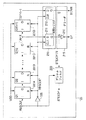
図2は本発明の好ましい実施例に従ったAVSスラックタイム検出器125を詳細に示す。AVSスラックタイム検出器125は典型的な遅延セル201A,201B,201Cおよび201Dを含むN個の逐次遅延セル201、インバータ205、状態レジスタ210、デコーダ215、およびデジタルフィルタ220を含んでいる。状態レジスタ210は、さらに、エッジトリガフリップフロップ(FF)211およびエッジトリガフリップフロップ(FF)212を含んでいる。デコーダ215はインバータ216を含んでいる。
FIG. 2 shows in detail an AVS
REGCLKクロック信号の立上りエッジはN逐次遅延セル201のチェーン内の各遅延セル中を逐次リップルする。N遅延セル201は同一コンポーネントでありDSP/CPUシステム120内のゲートと同じ工程から作られる。このようにして、N遅延セルのチェーン内の各遅延セルがその入力(I)およびその出力(O)間に可変伝播遅延Dを有し、それは他の全てのN遅延セル201の可変伝播遅延Dに実質的に等しい。伝播遅延が可変と言われるのは電源VDDのレベルが伝播遅延Dに影響を及ぼすためである。VDDが増加すると、N遅延セル201の各々の伝播遅延Dが減少する。VDDが減少すると、N遅延セル201の各々の伝播遅延Dが増加する。
The rising edge of the REGCLK clock signal sequentially ripples through each delay cell in the chain of N
このようにして、VDDの定められた値に対して、第1の遅延セル(すなわち、遅延セル201A)の入力からK遅延セル(すなわち、遅延セル201C)の出力までの結合伝播遅延はK・D(すなわち、DのK倍)となる。典型的な遅延セル201A,201B,201Cおよび201Dはそれらの各遅延期間D1,D2,D(K),およびD(K+1)により逐次表示される。第1の遅延セルの入力からK遅延セルの出力までの結合伝播遅延K×Dはa≠1の場合適切な係数によりスケーリングされた、M伝播遅延の安全マージンを含む、DSP/CPUシステム120を通る最長伝播遅延をモデル化するように設計される。たとえば、DSP/CPUシステム120を通る最長伝播遅延が6D(すなわち、6伝播遅延)以下であれば、Kの値を8に設定して、K遅延セルの出力は8伝播遅延(8D)を表し安全マージンMは2伝播遅延となるようにすることができる。別の実施例では、Kの値を7に設定して、K遅延セルの出力は7伝播遅延(7D)を表し安全マージンMは1伝播遅延となるようにすることができる。さらにもう一つの実施例では、Kの値を9に設定して、K遅延セルの出力は9伝播遅延(9D)を表し安全マージンMは3伝播遅延となるようにすることができる。
Thus, for a given value of VDD, the combined propagation delay from the input of the first delay cell (ie, delay
VDDの値が増加するとDSP/CPUシステム120を通る最長伝播遅延は減少し、VDDの値が減少するとDSP/CPUシステム120を通る最長伝播遅延は増加する。しかしながら、遅延セル201はDSP/CPUシステム120内のゲートと同じ工程から作り出されるため、K遅延セル(すなわち、遅延セル201C)の出力における結合遅延K・Dは比例的に変化してDSP/CPUシステム120を通る最長伝播遅延を追跡する。AVSスラックタイム検出器125の目的は遅延セル201Aの入力において受信されたREGCLKクロック信号の立上りエッジは、REGCLKクロック信号の降下エッジが受信される時間までに、K遅延セル(すなわち、遅延セル201C)の出力に伝播するがK+1遅延セルの出力に伝播しないようにVDDのレベルを制御することである。立上りエッジがK+1遅延セル(すなわち、遅延セル201D)の出力へまたはそれを超えて伝播すれば、VDDはREGCLKクロック信号の現在のクロック速度に対して大きすぎ電力が浪費される。立上りエッジが少なくともK遅延セル(すなわち、遅延セル201C)の出力までは伝播しなければ、VDDはREGCLKクロック信号の現在のクロック速度に対して低すぎてDSP/CPUシステム120を通る最長伝播遅延によるエラーを生じることがある。
As the VDD value increases, the longest propagation delay through the DSP /
図3は図2に示す典型的な実施例に従ったAVSスラックタイム検出器125の動作を示すタイミング図である。一つのクロックパルスが例示されている。最初に、REGCLKクロック信号はローである(論理0)。インバータ205はREGCLKクロック信号を反転してREGCLK*クロック信号を作り出し、それはN遅延セル201の各々のリセット(R)入力に加えられる。最初に、REGCLK*クロック信号はハイ(論理1)であり、それは各遅延セル201の出力(O)を論理0にする。
FIG. 3 is a timing diagram illustrating the operation of the AVS
REGCLKクロック信号が論理1(すなわち、クロックパルスの立上りエッジ)になると、REGCLK*クロック信号は論理0となって、全ての遅延セル201からリセット(R)信号を除去する。第1の伝播遅延D1後に、Tap 1と呼ばれる遅延セル201Aの出力は論理1となる(点線で示す)。第2の伝播遅延D2後に、Tap 2と呼ばれる遅延セル201Bの出力は論理1となる。立上りエッジはN遅延セル201のチェーン中を伝播し続ける。K伝播遅延D(K)後に、Tap Kと呼ばれる遅延セル201Cの出力は論理1となる(点線で示す)。
When the REGCLK clock signal goes to logic 1 (ie, the rising edge of the clock pulse), the REGCLK * clock signal goes to
K+1伝播遅延D(K+1)後に、Tap K+1と呼ばれる遅延セル201Dの出力は通常論理1となる。しかしながら、REGCLKクロック信号の降下エッジはK+1伝播遅延が完了する前に生じる。REGCLKクロック信号の降下エッジによりREGCLK*クロック信号は論理1(すなわち、立上りエッジ)となり、N遅延セル201の全てにリセット(R)信号を加えて全遅延セル201の出力(O)を論理0にリセットし戻す。
After K + 1 propagation delay D (K + 1), the output of
状態レジスタ210内のフリップフロップ(FF)211は遅延セル201C(すなわち、Tap K)の出力をモニタし、状態レジスタ210内のフリップフロップ(FF)212は遅延セル201D(すなわち、Tap K+1)の出力をモニタする。REGCLK*クロック信号の立上りエッジによりFF211およびFF212は出力がリセットされる前に遅延セル201Cおよび201Dの出力の値を読み取る。このようにして、STATUS(A,B)と言われる遅延セル201Cおよび201Dの出力の状態がREGCLKクロック信号の降下エッジ(すなわち、REGCLK*クロック信号の立上りエッジ)毎に読み出される。
The flip-flop (FF) 211 in the
最適状況下で、REGCLKクロック信号の立上りエッジはK遅延セル(すなわち、遅延セル201C)の出力までしか伝播しない。このようにして、最適状況下では、A=1,B=0,およびSTATUS(A,B)=10である。VDDが低すぎると、REGCLKクロック信号の立上りエッジはK遅延セルの出力まで伝播するのに失敗しSTATUS(A,B)=00である。VDDが高すぎると、REGCLKクロック信号の立上りエッジは少なくともK+1遅延セルの出力まで伝播しSTATUS(A,B)=11である。 Under optimal conditions, the rising edge of the REGCLK clock signal propagates only up to the output of the K delay cell (ie, delay cell 201C). Thus, under optimum circumstances, A = 1, B = 0, and STATUS (A, B) = 10. If VDD is too low, the rising edge of the REGCLK clock signal fails to propagate to the output of the K delay cell and STATUS (A, B) = 00. If VDD is too high, the rising edge of the REGCLK clock signal propagates to at least the output of the K + 1 delay cell and STATUS (A, B) = 11.
デコーダ215はSTATUS(A,B)の値を読み取ってVDDを増加する制御信号UPおよびVDDを減少する制御信号DOWNを作り出す。最適状況下では、STATUS(A,B)=10であり、UP=0およびDOWN=0となってVDDは変更されない。VDDが低すぎると、STATUS(A,B)=00であり、UP=1およびDOWN=0となってVDDは増加する。VDDが高すぎると、STATUS(A,B)=11であり、UP=0およびDOWN=1となってVDDは減少する。
The
典型的な実施例では、K遅延セル出力に対応するAの値は生信号STEADYINを表す。STEADY IN信号はVDDの値が安定レベルに調節されるまで0および1間で変動する。デジタルフィルタ220がSTEADY INを受信してその出力におけるSTEADY信号を論理1に設定する前にいつSTEADY INが論理1で安定となっているかを決定し、AVSクロック発生器115をイネーブルする。たとえば、デジタルフィルタ220はSTEADY信号が論理1に設定される前にSTEADY IN=1の10連続値をカウントするカウンタとすることができる。10のカウントに達する前にSTEADY INが論理0に切り替わると、カウンタはゼロにリセットされカウントをやり直す。
In the exemplary embodiment, the value of A corresponding to the K delay cell output represents the raw signal STEADYIN. The STEADY IN signal varies between 0 and 1 until the value of VDD is adjusted to a stable level. Before
図4Aは本発明の第1の典型的な実施例に従った典型的な遅延セル201を示す。遅延セル201はインバータ401およびNORゲート402を含んでいる。リセット信号(R)が論理1であれば、NORゲート402の出力(O)は論理0とされ入力(I)は無関係である。リセット信号(R)が論理0であれば、入力IはNORゲート402の出力(O)に通過することができる。このようにして、R=0であれば、遅延セル201の入力(I)における立上りエッジはインバータ401により反転されNORゲート401により再度反転される。このようにして、全遅延がインバータ401およびNORゲート402の結合伝播遅延に等しくなった後で、遅延セル201の出力(O)に立上りエッジが現れる。
FIG. 4A shows an
図4Bは本発明の第2の典型的な実施例に従った典型的な遅延セル201を示す。遅延セル201はNORゲート402および、典型的なインバータ401Aおよび401Bを含む、奇数個の逐次インバータ401、およびNORゲート402を含んでいる。リセット信号(R)が論理1であれば、NORゲート402の出力(O)は論理0とされ入力(I)は無関係である。リセット信号(R)が論理0であれば、入力IはNORゲート402の出力(O)に通過することができる。このようにして、R=0であれば、遅延セル201の入力(I)における立上りエッジはインバータ401Aから401Bにより奇数回逐次反転され、次に、NORゲート402により最後に1回反転される。このようにして、遇数回の反転が行われNORゲート402および全インバータ401Aから401Bの結合伝播遅延に等しい全遅延の後で、遅延セル201の出力(O)に立上りエッジが現れる。このようにして、遅延セル201の全遅延はその中のインバータ401の数を変えることにより操作することができる。また、当業者ならば反転機能を実施する他のタイプのゲートを単純なインバータ401の替わりに使用できることを認識できる。一般的に、入力Iを受信して反転出力I*を発生する任意のタイプのゲートを使用することができる。
FIG. 4B shows an
図5は本発明の別の実施例に従ったAVSスラックタイム検出器125を詳細に示す。図2に例示されたAVSスラックタイム検出器125の第1の実施例は2つの制御信号、すなわちUPおよびDOWN、を作り出しそれを使用してVDDのレベルを比較的粗い増分ステップまたは比較的粗い減分ステップで調節することができた。図5に示す典型的な実施例では、AVSスラックタイム検出器125はVDDのレベルを比較的少量および比較的大量増減分するのに使用できる複数の制御信号を作り出す。
FIG. 5 illustrates in detail an AVS
図5のAVSスラックタイム検出器125は大概の点において図2に例示されたAVSスラックタイム検出器125と同一である。主要な違いはモニタされる遅延セル201出力数である。図2のAVSスラックタイム検出器125は2つの遅延セル201出力(すなわち、KおよびK+1)しかモニタしなかった。図5のAVSスラックタイム検出器125は3つ以上の遅延セル201の出力をモニタする。図5において、状態レジスタ210は合計P+1の遅延セル201出力を表すTap RからTap R+Pの出力をモニタする。
The AVS
DSP/CPUシステム120を通る最長伝播遅延が6D(すなわち、6伝播遅延)以下である典型的な実施例について考える。安全マージンMが1伝播遅延でありかつPが3に等しければ、Tap Rは第7遅延セルの出力であり、Tap R+1は第8遅延セルの出力であり、Tap R+2は第9遅延セルの出力であり、Tap R+3は第10遅延セルの出力である。これら4つの遅延セル出力は、それぞれ、K−1遅延セル、K遅延セル、K+1遅延セル、およびK+2遅延セルの出力を表す。
Consider an exemplary embodiment where the longest propagation delay through the DSP /
ここでも、AVSスラックタイム検出器125の目的は、REGCLKクロック信号の降下エッジが受信される時間までに、遅延セル201Aの入力において受信されたREGCLKクロック信号の立上りエッジはK遅延セル(Tap R+1)の出力に伝播するがK+1遅延セル(Tap R+2)の出力には伝播しないようにVDDのレベルを制御することである。このようにして、最適状況下で、STATUS(K−1,K,K+1,K+2)=1100である。しかしながら、図2の場合とは異なり、図5のデコーダ215はSTATUS(K−1,K,K+1,K+2)の値に従って異なる増分ステップサイズまたは減分ステップサイズを有する複数のVDD制御信号を発生することができる。
Again, the purpose of the AVS
たとえば、STATUS(K−1,K,K+1,K+2)が0000であれば、デコーダ215はVDDを比較的大きい量(たとえば、+0.1Vステップサイズ)だけ増分するLARGE UP制御信号を発生することができる。これは大きなエラーに対してVDDをより迅速に訂正する。STATUS(K−1,K,K+1,K+2)が1000であれば、デコーダ215はVDDを比較的小さい量(たとえば、+0.01Vステップサイズ)だけ増分するSMALL UP制御信号を発生することができる。これは小さなエラーに対してオーバシュートを生じることなくVDDを小さい量だけ増分する。
For example, if STATUS (K-1, K, K + 1, K + 2) is 0000,
たとえば、STATUS(K−1,K,K+1,K+2)が1111であれば、デコーダ215はVDDを比較的大きい量(たとえば、−0.1Vステップサイズ)だけ減分するLARGE DOWN制御信号を発生することができる。これは大きなエラーに対してVDDをより迅速に訂正する。STATUS(K−1,K,K+1,K+2)が1110であれば、デコーダ215はVDDを比較的小さい量(たとえば、−0.01Vステップサイズ)だけ減分するSMALL DOWN制御信号を発生することができる。これは小さなエラーに対してアンダーシュートを生じることなくVDDを小さい量だけ減分する。
For example, if STATUS (K-1, K, K + 1, K + 2) is 1111, the
本発明のさらにもう一つの実施例では、状態レジスタ210は、たとえば、6遅延セル201出力をモニタしてVDDのレベルの微調整および粗調整の度合いをさらに高めることができる。たとえば、最適状況下で、STATUS(K−2,K−1,K,K+1,K+2,K+3)=111000である。STATUS(K−2,K−1,K,K+1,K+2,K+3)=000000,100000,または110000であれば、デコーダ215は、それぞれ、LARGE UP,MEDIUM UPまたはSMALL UP制御信号を発生することができる。STATUS(K−2,K−1,K,K+1,K+2,K+3)=111111,111110または111100であれば、デコーダ215は、それぞれ、LARGE DOWN,MEDIUM DOWNおよびSMALL DOWN制御信号を発生することができる。
In yet another embodiment of the present invention, the
前記実施例では、AVSスラックタイム検出器125の動作は2つのトリガイベント、すなわち、スラックタイムをモニタしてVDDのレベルを制御するのに使用されるREGCLKクロック信号の最初に生じる立上りエッジおよびその引き続く降下エッジに関して記述された。しかしながら、これは単なる図解のためであり本発明の範囲を制限するものと解釈してはならない。当業者ならばREGCLKクロック信号の最初に生じる降下エッジおよびその引き続く立上りエッジをトリガイベントとして使用してスラックタイムをモニタしVDDのレベルを制御するようにAVSスラックタイム検出器125を容易に再構成できることを認識できる。
In the above embodiment, the operation of the AVS
図6にフロー図を示し、それは本発明の典型的な実施例に従ったデジタル処理システム100内のAVSスラックタイム検出器125の動作を図解している。最初に、DSP/CPUシステム120が新しい公称クロック動作速度(たとえば、50MHz)を確立するためのFREQUENCY CONTROL信号の値を設定する(プロセスステップ605)。次に、AVSスラックタイム検出器125はREGCLK信号をモニタしており、もしあれば、スラックタイムの量を決定する。前記したように、スラックタイムはDSP/CPUシステム120内の最長伝播遅延とREGCLK信号のパルス幅間の時間差である(プロセスステップ610)。DSP/CPUシステム120内の最長伝播遅延はK遅延セル201の出力における全遅延K×Dで表され、REGCLKクロック信号のパルス幅はその立上りクロックエッジと次の降下クロックエッジ間の時間長である。あるいは、REGCLKクロック信号のパルス幅はその降下クロックエッジと次の立上りクロックエッジ間の時間長である。スラックタイムが大きすぎると、VDDは減分される(プロセスステップ615および620)。スラックタイムが小さすぎると、VDDは増分される(プロセスステップ625および630)。そうでなければ、AVSスラックタイム検出器125はREGCLK信号をモニタし続け、もしあれば、スラックタイムの量を決定する(プロセスステップ610)。
A flow diagram is shown in FIG. 6, which illustrates the operation of the AVS
図7は本発明の第1の典型的な実施例に従ったAVSクロック発生器115のブロック図である。第1の典型的な実施例では、AVSクロック発生器115はクロックデバイダ回路705(“Nで分割”と表示)、クロックデバイダ回路710(“N2で分割”と表示)、および制御ブロック715を含むクロック制御回路を提供する。AVSクロック発生器115はデジタル処理コンポーネント120に選択的にクロック信号を加えるように操作できる。クロック信号は複数の動作周波数に変更することができる。
FIG. 7 is a block diagram of the
典型的なクロックデバイダ回路705は、入力として、水晶発振器105からのCLKEXT信号およびDSP/CPUシステム120からのFREQUENCY CONTROL信号Nを受信する。典型的なクロックデバイダ回路710は、入力として、水晶発振器105からのCLKEXT信号および制御ブロック715からの第2のFREQUENCY CONTROL信号N2を受信する。典型的な制御ブロック715は、入力として、AVSスラックタイム検出器125からのSTEADY信号およびDSP/CPUシステム120からのFREQUENCY CONTROL信号Nを受信する。
A typical
FREQUENCY CONTROL信号の受信に応答して、制御ブロック715はDSP/CPUシステム120に加えられたCLK信号を停止する。次に、クロックデバイダ回路705はCLKEXT信号をFREQUENCY CONTROL信号で除すことによりREGCLK信号を新しいクロック速度に設定する。次に、AVS電源130のレベルがAVSスラックタイム検出器125により新しいクロック速度に対する最適値に調節される間に、制御ブロック715はSTEADY信号をモニタする。
In response to receiving the FREQUENCY CONTROL signal, the control block 715 stops the CLK signal applied to the DSP /
AVSスラックタイム検出器125からのイネーブルされたSTEADY信号の受信に応答して、制御ブロック715はクロックデバイダ回路710をイネーブルし、それはCLKEXT信号を第2のFREQUENCY CONTROL信号値Nで除すことにより新しいCLK信号を発生してDSP/CPUシステム120に加える。定常状態では、第2のFREQUENCY CONTROL信号N2はFREQUENCY CONTROL信号Nに等しいか、あるいは定数によりスケーリングされる。
In response to receiving the enabled STEADY signal from the AVS
図8は本発明の第2の典型的な実施例に従ったAVSクロック発生器115のブロック図である。第2の典型的な実施例では、AVSクロック発生器115はやはりDSP/CPUシステム120に選択的にクロック信号を与えるクロック制御回路を提供し、クロックデバイダ回路805(“Nで分割”と表示)、ANDゲート810、および制御ブロック815を含んでいる。
FIG. 8 is a block diagram of an
クロックデバイダ回路705は、入力として、水晶発振器105からのCLKEXT信号およびDSP/CPUシステム120からのFREQUENCY CONTROL信号Nを受信する。ANDゲート810は、入力として、クロックデバイダ回路705からのREGCLK信号および制御ブロック815からのENABLE信号を受信する。典型的な制御ブロック815は、入力として、AVSスラックタイム検出器125からのSTEADY信号およびDSP/CPUシステム120からのFREQUENCY CONTROL信号Nを受信する。
The
ここでも、FREQUENCY CONTROL信号の受信に応答して、制御ブロック715はENABLE信号を論理0に設定することによりDSP/CPUシステム120に加えられたCLK信号を停止する。次に、クロックデバイダ回路705はCLKEXT信号をFREQUENCY CONTROL信号で除すことによりREGCLK信号を新しいクロック速度に設定する。次に、AVS電源130のレベルがAVSスラックタイム検出器125により新しいクロック速度に対する最適値に調節される間に、制御ブロック715はSTEADY信号をモニタする。AVSスラックタイム検出器125からのイネーブルされたSTEADY信号の受信に応答して、ANDゲート810をイネーブルし新しいCLK信号(REGCLK)をDSP/CPUシステム120に加えるために、制御ブロック715はENABLE信号を論理1に設定する。
Again, in response to receiving the FREQUENCY CONTROL signal, the control block 715 stops the CLK signal applied to the DSP /
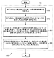
図9はフロー図900を示し、それは本発明の原理に従ったAVSクロック発生器115の動作を図解している。最初に、AVSクロック発生器115はDSP/CPUシステム120から新しいFREQUENCY CONTROL値Nを受信する(プロセスステップ905)。クロック速度の変化に応答して、AVSクロック発生器115はDSP/CPUシステム120に加えられたCLK信号を停止する(プロセスステップ910)。次に、AVSクロック発生器115はREGCLK信号を新しいクロック速度に設定しVDD電源のレベル(あるいは、随意デジタル処理システム100の他の動作パラメータ)が新しいクロック速度に対する最適値に調節される間、STEADY信号をモニタする(プロセスステップ915)。STEADY信号が最後に再イネーブルされると(すなわち、STEADY信号上に立上りエッジが生じる)、AVSクロック発生器115はCLK信号を新しいクロック速度に設定してDSP/CPUシステム120CLK信号を再び加える(プロセスステップ920)。
FIG. 9 shows a flow diagram 900 that illustrates the operation of the
概括的に言えば、本発明の有利な実施例はクロック信号が複数の動作周波数に変更できるデジタル処理コンポーネントに選択的にクロック信号を加えるクロック制御回路に向けられている。クロック制御回路は(i)第1の動作周波数を第2の動作周波数に変更するコマンドを受信する、(ii)コマンドに応答して加えられたクロック信号をディセーブルする、(iii)第2の動作周波数を有するテストクロック信号を発生する、(iv)テストクロック信号を電源調節回路に加える、および(v)電源調節回路からの状態信号を感知するように操作できる。状態信号はデジタル処理コンポーネントの電源レベルが第2の動作周波数に対して適切な最適値に調節されていることを示す。 Generally speaking, the preferred embodiment of the present invention is directed to a clock control circuit that selectively applies a clock signal to a digital processing component in which the clock signal can be changed to a plurality of operating frequencies. The clock control circuit (i) receives a command to change the first operating frequency to the second operating frequency, (ii) disables a clock signal applied in response to the command, (iii) a second It can be operated to generate a test clock signal having an operating frequency, (iv) apply the test clock signal to the power supply adjustment circuit, and (v) sense a status signal from the power supply adjustment circuit. The status signal indicates that the power level of the digital processing component is adjusted to an optimal value appropriate for the second operating frequency.
本発明を詳細に記述してきたが、当業者なら最も広範な形の本発明の精神および範囲を逸脱することなく、それらをさまざまに修正、置換および変更できることを理解しなければならない。 Although the invention has been described in detail, it should be understood by those skilled in the art that various modifications, substitutions and alterations can be made without departing from the spirit and scope of the invention in its broadest form.
Claims (15)
連続して直列接続された複数の遅延セルであって、前記遅延セルの各々が電源レベルの値により決定される遅延時間を有し、最初の遅延セルの入力に加えられる前記テストクロック信号のクロックエッジが前記複数の遅延セル中を次々に伝播するようにされた複数の遅延セルと
を有する装置であって、
前記電源調節回路は(a)少なくとも第1の特定の遅延セルおよび第2の特定の遅延セルの出力をモニタする、(b)前記クロックエッジが前記第1の特定の遅延セルの出力に達しかつ前記第2の特定の遅延セルの出力に達していないかどうかを識別する、および(c)前記クロックエッジが前記第1の特定の遅延セルの前記出力に達していない時または前記クロックエッジが前記第2の特定の遅延セルの前記出力に達した時に前記電源レベルを調節する制御信号を発生するように動作する前記装置。 A clock control circuit for selectively applying a clock signal to a digital processing component, wherein the clock signal can be changed to a plurality of operating frequencies, and (i) changing a first operating frequency to a second operating frequency. Receiving a command; (ii) in response to the command, disabling the supply of a clock signal to the digital processing component; (iii) generating a test clock signal having the second operating frequency; ) Applying the test clock signal to a power conditioning circuit; and (v) a status signal from the power conditioning circuit indicating that the power level of the digital processing component is regulated for use at the second operating frequency. Sensing, and (vi) setting the clock signal to the second operating frequency in response to the status signal, To work, and the clock control circuit,
A plurality of delay cells connected in series in series, each of the delay cells having a delay time determined by a value of a power supply level, and the clock of the test clock signal applied to the input of the first delay cell A plurality of delay cells whose edges are adapted to propagate one after another through the plurality of delay cells,
The power conditioning circuit (a) monitors the output of at least a first specific delay cell and a second specific delay cell; (b) the clock edge reaches the output of the first specific delay cell; Identifying whether the output of the second specific delay cell has not been reached, and (c) when the clock edge has not reached the output of the first specific delay cell or when the clock edge is The apparatus operative to generate a control signal that adjusts the power supply level when the output of a second particular delay cell is reached.
前記第2の動作周波数を有する前記テストクロック信号を発生するように動作するクロックデバイダ回路、および
前記受信したコマンドに応答して前記デジタル処理コンポーネントへの前記クロック信号の前記供給をディセーブルし、前記状態信号に応答して前記デジタル処理コンポーネントへの前記クロック信号の前記供給をイネーブルするように動作するコントローラ
を含む装置。 The apparatus according to claim 1, wherein the clock control circuit includes:
A clock divider circuit operable to generate the test clock signal having the second operating frequency; and disabling the supply of the clock signal to the digital processing component in response to the received command; An apparatus comprising: a controller operable to enable the supply of the clock signal to the digital processing component in response to a status signal.
第1の動作周波数を第2の動作周波数に変更するコマンドを受信するステップと、
前記コマンドに応答して、前記デジタル処理コンポーネントへのクロック信号の供給をディセーブルするステップと、
前記第2の動作周波数を有するテストクロック信号を発生するステップと、
前記テストクロック信号を、連続して直列接続された前記複数の遅延セルうちの最初の遅延セルに加えて、その結果前記最初の遅延セルの入力に加えられるテストクロック信号のクロックエッジが前記複数の遅延セル中を次々に伝播すると共に、前記遅延セルの各々が前記デジタル処理コンポーネントの電源レベルの値により決定される遅延時間を有するステップと、
少なくとも、電源調節回路において第1の特定の遅延セルおよび第2の特定の遅延セルの出力をモニタするステップと、
前記テストクロックのクロックエッジが前記第1の特定の遅延セルの出力に達しかつ前記第2の特定の遅延セルの出力に達していないかどうかを識別するステップと、
前記クロックエッジが前記第1の特定の遅延セルの前記出力に達していない時または前記クロックエッジが前記第2の特定の遅延セルの前記出力に達した時に前記電源レベルを調節する制御信号を発生するステップと、
前記デジタル処理コンポーネントの電源レベルが前記第2の動作周波数の使用用に調節されていることを示す前記電源調節回路からの状態信号を感知するステップと、
前記状態信号に応答して、前記クロック信号を前記第2の動作周波数に設定するステップと
を含む動作方法。 An operation method of a clock control circuit that selectively applies a clock signal to a digital processing component, wherein the clock signal can be changed to a plurality of operation frequencies, and the operation method of the clock control circuit includes:
Receiving a command to change the first operating frequency to the second operating frequency;
In response to the command, disabling the supply of a clock signal to the digital processing component;
Generating a test clock signal having the second operating frequency;
The test clock signal is added to the first delay cell of the plurality of delay cells connected in series, and as a result, the clock edge of the test clock signal applied to the input of the first delay cell is the plurality of delay cells. Propagating through the delay cells one after the other, each of the delay cells having a delay time determined by the value of the power level of the digital processing component;
Monitoring at least the outputs of the first specific delay cell and the second specific delay cell in the power supply regulation circuit;
Identifying whether a clock edge of the test clock has reached the output of the first specific delay cell and has not reached the output of the second specific delay cell;
Generate a control signal to adjust the power level when the clock edge does not reach the output of the first specific delay cell or when the clock edge reaches the output of the second specific delay cell And steps to
Sensing a status signal from the power conditioning circuit indicating that a power level of the digital processing component is adjusted for use of the second operating frequency;
Setting the clock signal to the second operating frequency in response to the status signal.
前記第2の動作周波数を有する前記テストクロック信号を発生するように動作するクロックデバイダ回路、および
前記受信したコマンドに応答して前記デジタル処理コンポーネントへの前記クロック信号の前記供給をディセーブルし、前記状態信号に応答して前記デジタル処理コンポーネントへの前記クロック信号の前記供給をイネーブルするように動作するコントローラ
を含む方法。 6. The method of claim 5, wherein the clock control circuit is
A clock divider circuit operable to generate the test clock signal having the second operating frequency; and disabling the supply of the clock signal to the digital processing component in response to the received command; A controller operative to enable the supply of the clock signal to the digital processing component in response to a status signal.
前記デジタル処理コンポーネントに可変電源レベルVDDを供給することができる可調節電源と、
前記VDDを調節することができる電源調節回路と、
前記デジタル処理コンポーネントに選択的にクロック信号を加えるクロック制御回路であって、前記クロック信号は複数の動作周波数に変更することができ、前記クロック制御回路は(i)第1の動作周波数を第2の動作周波数に変更するコマンドを受信する、(ii)前記コマンドに応答して、前記クロック信号の前記デジタル処理コンポーネントへの供給をディセーブルする、(iii)前記第2の動作周波数を有するテストクロック信号を発生する、(iv)前記テストクロック信号を前記電源調節回路に加える、(v)前記デジタル処理コンポーネントの電源レベルが前記第2の動作周波数での使用用に調節されていることを示す前記電源調節回路からの状態信号を感知する、および(vi)前記状態信号に応答して前記クロック信号を前記第2の動作周波数に設定する、ように動作するクロック制御回路と、
連続して直列接続された複数の遅延セルであって、前記遅延セルの各々が前記VDDの値により決定される遅延時間を有し、最初の遅延セルの入力に加えられる前記テストクロック信号のクロックエッジが前記複数の遅延セル中を次々に伝播するようにされた複数の遅延セルと
を含むデジタル回路であって、
前記電源調節回路は(a)少なくとも第1の特定の遅延セルおよび第2の特定の遅延セルの出力をモニタする、(b)前記クロックエッジが前記第1の特定の遅延セルの出力に達しかつ前記第2の特定の遅延セルの出力に達していないかどうかを識別する、および(c)前記クロックエッジが前記第1の特定の遅延セルの前記出力に達していない時または前記クロックエッジが前記第2の特定の遅延セルの前記出力に達した時に前記VDDを調節する制御信号を発生するように動作するデジタル回路。 Digital processing components that can operate at different clock frequencies;
An adjustable power supply capable of supplying a variable power supply level VDD to the digital processing component;
A power supply adjustment circuit capable of adjusting the VDD;
A clock control circuit for selectively applying a clock signal to the digital processing component, wherein the clock signal can be changed to a plurality of operating frequencies, wherein the clock control circuit (i) sets a first operating frequency to a second operating frequency. (Ii) in response to the command, disable the supply of the clock signal to the digital processing component; (iii) a test clock having the second operating frequency Generating a signal; (iv) applying the test clock signal to the power conditioning circuit; (v) indicating that the power level of the digital processing component is regulated for use at the second operating frequency. Sensing a status signal from a power conditioning circuit; and (vi) responding to the status signal with the clock signal. Setting the second operating frequency, a clock control circuit operative to,
A plurality of delay cells connected in series in series, each of the delay cells having a delay time determined by the value of VDD, and the clock of the test clock signal applied to the input of the first delay cell A plurality of delay cells whose edges are adapted to propagate one after another through the plurality of delay cells,
The power conditioning circuit (a) monitors the output of at least a first specific delay cell and a second specific delay cell; (b) the clock edge reaches the output of the first specific delay cell; Identifying whether the output of the second specific delay cell has not been reached, and (c) when the clock edge has not reached the output of the first specific delay cell or when the clock edge is A digital circuit that operates to generate a control signal that adjusts the VDD when the output of a second particular delay cell is reached.
前記第2の動作周波数を有する前記テストクロック信号を発生するように動作するクロックデバイダ回路、および
前記受信したコマンドに応答して前記デジタル処理コンポーネントへの前記クロック信号の前記供給をディセーブルし、前記状態信号に応答して前記デジタル処理コンポーネントへの前記クロック信号の前記供給をイネーブルするように動作するコントローラ
を含むデジタル回路。 9. The digital circuit according to claim 8, wherein the clock control circuit is
A clock divider circuit operable to generate the test clock signal having the second operating frequency; and disabling the supply of the clock signal to the digital processing component in response to the received command; A digital circuit including a controller operative to enable the supply of the clock signal to the digital processing component in response to a status signal.
前記電源調節回路は、
前記クロックエッジが前記第3の特定の遅延セルの出力に到達していない場合、比較的大きな増分値で前記VDDを増加させ、
前記クロックエッジが前記第3の特定の遅延セルの出力に到達していてかつ前記第1の特定の遅延セルの出力に到達していない場合、比較的小さな増分値で前記VDDを増加させ、
前記クロックエッジが前記第2の特定の遅延セルの出力に到達していてかつ前記第4の特定の遅延セルの出力に到達していない場合、比較的小さな減分値で前記VDDを減少させ、
前記クロックエッジが前記第2の特定の遅延セルおよび前記第4の特定の遅延セルの出力に到達している場合、比較的大きな減分値で前記VDDを減少させるように
前記VDDを調節する制御信号を発生するように動作する前記デジタル回路。
15. A digital circuit according to claim 14, comprising:
The power supply adjustment circuit includes:
If the clock edge has not reached the output of the third specific delay cell, increase VDD by a relatively large increment value;
If the clock edge has reached the output of the third specific delay cell and has not reached the output of the first specific delay cell, increase VDD by a relatively small increment value;
If the clock edge has reached the output of the second specific delay cell and has not reached the output of the fourth specific delay cell, the VDD is decreased by a relatively small decrement value;
Control that adjusts the VDD to decrease the VDD by a relatively large decrement value when the clock edge reaches the output of the second specific delay cell and the fourth specific delay cell. Said digital circuit operating to generate a signal;
Applications Claiming Priority (2)
| Application Number | Priority Date | Filing Date | Title |
|---|---|---|---|
| US10/053,227 | 2002-01-19 | ||
| US10/053,227 US6944780B1 (en) | 2002-01-19 | 2002-01-19 | Adaptive voltage scaling clock generator for use in a digital processing component and method of operating the same |
Related Parent Applications (1)
| Application Number | Title | Priority Date | Filing Date |
|---|---|---|---|
| JP2003562769A Division JP2006502466A (en) | 2002-01-19 | 2003-01-17 | Adaptive voltage scaling clock generator for use in digital processing components and method of operation thereof |
Publications (2)
| Publication Number | Publication Date |
|---|---|
| JP2010040053A true JP2010040053A (en) | 2010-02-18 |
| JP4825291B2 JP4825291B2 (en) | 2011-11-30 |
Family
ID=27609118
Family Applications (2)
| Application Number | Title | Priority Date | Filing Date |
|---|---|---|---|
| JP2003562769A Pending JP2006502466A (en) | 2002-01-19 | 2003-01-17 | Adaptive voltage scaling clock generator for use in digital processing components and method of operation thereof |
| JP2009235368A Expired - Fee Related JP4825291B2 (en) | 2002-01-19 | 2009-10-09 | Adaptive voltage scaling clock generator for use in digital processing components and method of operation thereof |
Family Applications Before (1)
| Application Number | Title | Priority Date | Filing Date |
|---|---|---|---|
| JP2003562769A Pending JP2006502466A (en) | 2002-01-19 | 2003-01-17 | Adaptive voltage scaling clock generator for use in digital processing components and method of operation thereof |
Country Status (5)
| Country | Link |
|---|---|
| US (1) | US6944780B1 (en) |
| JP (2) | JP2006502466A (en) |
| CN (1) | CN100511098C (en) |
| AU (1) | AU2003209296A1 (en) |
| WO (1) | WO2003062972A2 (en) |
Cited By (1)
| Publication number | Priority date | Publication date | Assignee | Title |
|---|---|---|---|---|
| US11928003B2 (en) | 2019-11-19 | 2024-03-12 | Sony Semiconductor Solutions Corporation | Voltage control device |
Families Citing this family (23)
| Publication number | Priority date | Publication date | Assignee | Title |
|---|---|---|---|---|
| US7149903B1 (en) * | 2002-12-18 | 2006-12-12 | National Semiconductor Corporation | System and method for signal delay in an adaptive voltage scaling slack detector |
| GB2408116B (en) * | 2003-11-14 | 2006-09-20 | Advanced Risc Mach Ltd | Operating voltage determination for an integrated circuit |
| KR101136036B1 (en) * | 2003-12-24 | 2012-04-18 | 삼성전자주식회사 | Processor system and method for reducing power consumption in idle mode |
| CN1324421C (en) * | 2004-08-23 | 2007-07-04 | 联想(北京)有限公司 | Method and apparatus for central processor frequency conversion and central processor fan speed change |
| US7379718B2 (en) | 2004-12-20 | 2008-05-27 | Marvell World Trade Ltd. | Method and apparatus to manage power consumption of a semiconductor device |
| US7581120B1 (en) | 2005-05-23 | 2009-08-25 | National Semiconductor Corporation | System and method for providing multi-point calibration of an adaptive voltage scaling system |
| US7917799B2 (en) * | 2007-04-12 | 2011-03-29 | International Business Machines Corporation | Method and system for digital frequency clocking in processor cores |
| US7802216B2 (en) * | 2007-09-13 | 2010-09-21 | Rapid Bridge Llc | Area and power saving standard cell methodology |
| US7921312B1 (en) | 2007-09-14 | 2011-04-05 | National Semiconductor Corporation | System and method for providing adaptive voltage scaling with multiple clock domains inside a single voltage domain |
| KR100806295B1 (en) * | 2007-11-26 | 2008-02-22 | 주식회사 룩센테크놀러지 | Output voltage adaptive converter and method thereof |
| US7996743B1 (en) * | 2008-04-01 | 2011-08-09 | Altera Corporation | Logic circuit testing with reduced overhead |
| TWI374284B (en) * | 2008-12-16 | 2012-10-11 | Princeton Technology Corp | Logic tester and method for simultaneously measuring delay periods of multiple tested devices |
| HUE038104T2 (en) | 2009-03-30 | 2018-09-28 | Qualcomm Inc | Adaptive voltage scaling |
| US20110089914A1 (en) * | 2009-10-15 | 2011-04-21 | National Semiconductor Corporation | Apparatus and method for isolating an adaptive voltage scaling (AVS) loop in a powered system |
| US9093846B2 (en) | 2009-12-04 | 2015-07-28 | National Semiconductor Corporation | Methodology for controlling a switching regulator based on hardware performance monitoring |
| US8004329B1 (en) | 2010-03-19 | 2011-08-23 | National Semiconductor Corporation | Hardware performance monitor (HPM) with variable resolution for adaptive voltage scaling (AVS) systems |
| US8572426B2 (en) | 2010-05-27 | 2013-10-29 | National Semiconductor Corporation | Hardware performance monitor (HPM) with extended resolution for adaptive voltage scaling (AVS) systems |
| EP2883141A1 (en) | 2012-08-08 | 2015-06-17 | ST-Ericsson SA | Adaptive voltage scaling mechanism based on voltage shoot measurement |
| CN104951029A (en) * | 2014-03-25 | 2015-09-30 | 联芯科技有限公司 | Voltage supply method for CPUs in mobile terminals and mobile terminals |
| US9118458B1 (en) * | 2014-04-24 | 2015-08-25 | Telefonaktiebolaget L M Ericsson (Publ) | Clock phase alignment |
| CN104035018B (en) | 2014-06-12 | 2017-04-19 | 华为技术有限公司 | Voltage self-adaptive adjustment circuit and chip |
| US10587253B1 (en) | 2018-11-29 | 2020-03-10 | Qualcomm Incorporated | Ring oscillator-based programmable delay line |
| US11249530B1 (en) * | 2020-11-25 | 2022-02-15 | Qualcomm Incorporated | Adaptive voltage controller |
Citations (5)
| Publication number | Priority date | Publication date | Assignee | Title |
|---|---|---|---|---|
| JPH05158587A (en) * | 1991-12-11 | 1993-06-25 | Kyocera Corp | Information processor |
| JPH11296243A (en) * | 1998-04-13 | 1999-10-29 | Fujitsu Ltd | Power supply voltage adjusting circuit, semiconductor device and method for adjusting power supply voltage of semiconductor device |
| JP2000091506A (en) * | 1998-09-16 | 2000-03-31 | Matsushita Electric Ind Co Ltd | Semiconductor integrated circuit |
| JP2001505676A (en) * | 1996-08-07 | 2001-04-24 | モトローラ・セミコンデュクトゥール・ソシエテ・アノニム | Method and circuit for dynamically adjusting the supply voltage and / or the frequency of a clock signal in a digital circuit |
| JP2001159928A (en) * | 1999-12-01 | 2001-06-12 | Mitsubishi Electric Corp | Internal operation clock generation circuit provided with test function |
Family Cites Families (13)
| Publication number | Priority date | Publication date | Assignee | Title |
|---|---|---|---|---|
| US4231335A (en) * | 1979-04-06 | 1980-11-04 | Borg-Warner Corporation | Control system for regulating air/fuel ratio |
| JP3718251B2 (en) * | 1994-02-28 | 2005-11-24 | 株式会社ルネサステクノロジ | Data processing device |
| JPH08211960A (en) * | 1995-01-31 | 1996-08-20 | Mitsubishi Electric Corp | Microcomputer |
| US5812860A (en) * | 1996-02-12 | 1998-09-22 | Intel Corporation | Method and apparatus providing multiple voltages and frequencies selectable based on real time criteria to control power consumption |
| US6424184B1 (en) * | 1996-09-25 | 2002-07-23 | Matsushita Electric Industrial Co., Ltd. | Frequency-voltage conversion circuit, delay amount judgement circuit, system having frequency-voltage conversion circuit, method of adjusting input/output characteristics of frequency-voltage conversion circuit, and apparatus for automatically adjusting input |
| JPH10222253A (en) * | 1997-02-07 | 1998-08-21 | Hitachi Ltd | Information processing system |
| US5941631A (en) * | 1998-10-29 | 1999-08-24 | Bright Yin Huey Co., Ltd. | Pendent lamp structure |
| WO2001035200A1 (en) | 1999-11-09 | 2001-05-17 | Advanced Micro Devices, Inc. | Dynamically adjusting a processor's operational parameters according to its environment |
| US6664775B1 (en) * | 2000-08-21 | 2003-12-16 | Intel Corporation | Apparatus having adjustable operational modes and method therefore |
| US6498321B1 (en) * | 2001-04-09 | 2002-12-24 | Lincoln Global, Inc. | System and method for controlling an electric arc welder |
| WO2003021453A2 (en) | 2001-08-29 | 2003-03-13 | Analog Devices, Inc. | Generic serial port architecture and system |
| US6608528B2 (en) | 2001-10-22 | 2003-08-19 | Intel Corporation | Adaptive variable frequency clock system for high performance low power microprocessors |
| US7061292B2 (en) | 2001-11-09 | 2006-06-13 | The Regents Of The University Of Colorado | Adaptive voltage regulator for powered digital devices |
-
2002
- 2002-01-19 US US10/053,227 patent/US6944780B1/en not_active Expired - Lifetime
-
2003
- 2003-01-17 AU AU2003209296A patent/AU2003209296A1/en not_active Abandoned
- 2003-01-17 WO PCT/US2003/001647 patent/WO2003062972A2/en active Application Filing
- 2003-01-17 CN CNB038062046A patent/CN100511098C/en not_active Expired - Fee Related
- 2003-01-17 JP JP2003562769A patent/JP2006502466A/en active Pending
-
2009
- 2009-10-09 JP JP2009235368A patent/JP4825291B2/en not_active Expired - Fee Related
Patent Citations (5)
| Publication number | Priority date | Publication date | Assignee | Title |
|---|---|---|---|---|
| JPH05158587A (en) * | 1991-12-11 | 1993-06-25 | Kyocera Corp | Information processor |
| JP2001505676A (en) * | 1996-08-07 | 2001-04-24 | モトローラ・セミコンデュクトゥール・ソシエテ・アノニム | Method and circuit for dynamically adjusting the supply voltage and / or the frequency of a clock signal in a digital circuit |
| JPH11296243A (en) * | 1998-04-13 | 1999-10-29 | Fujitsu Ltd | Power supply voltage adjusting circuit, semiconductor device and method for adjusting power supply voltage of semiconductor device |
| JP2000091506A (en) * | 1998-09-16 | 2000-03-31 | Matsushita Electric Ind Co Ltd | Semiconductor integrated circuit |
| JP2001159928A (en) * | 1999-12-01 | 2001-06-12 | Mitsubishi Electric Corp | Internal operation clock generation circuit provided with test function |
Cited By (1)
| Publication number | Priority date | Publication date | Assignee | Title |
|---|---|---|---|---|
| US11928003B2 (en) | 2019-11-19 | 2024-03-12 | Sony Semiconductor Solutions Corporation | Voltage control device |
Also Published As
| Publication number | Publication date |
|---|---|
| WO2003062972A3 (en) | 2004-02-26 |
| US6944780B1 (en) | 2005-09-13 |
| CN100511098C (en) | 2009-07-08 |
| JP2006502466A (en) | 2006-01-19 |
| WO2003062972A2 (en) | 2003-07-31 |
| JP4825291B2 (en) | 2011-11-30 |
| AU2003209296A1 (en) | 2003-09-02 |
| CN1643480A (en) | 2005-07-20 |
Similar Documents
| Publication | Publication Date | Title |
|---|---|---|
| JP4825291B2 (en) | Adaptive voltage scaling clock generator for use in digital processing components and method of operation thereof | |
| US7117378B1 (en) | Adaptive voltage scaling digital processing component and method of operating the same | |
| US6548991B1 (en) | Adaptive voltage scaling power supply for use in a digital processing component and method of operating the same | |
| JP4567453B2 (en) | Method and apparatus for self-calibration to adaptively adjust power supply voltage in a digital processor | |
| US6985025B1 (en) | System for adjusting a power supply level of a digital processing component and method of operating the same | |
| JP3323207B2 (en) | Frequency-voltage conversion circuit, delay amount determination circuit, system including frequency-voltage conversion circuit, method for adjusting input / output characteristics of frequency-voltage conversion circuit, and apparatus for automatically adjusting input / output characteristics of frequency-voltage conversion circuit | |
| JP5706007B2 (en) | Semiconductor device with on-chip voltage regulator | |
| JP2001505676A (en) | Method and circuit for dynamically adjusting the supply voltage and / or the frequency of a clock signal in a digital circuit | |
| US8723571B2 (en) | Digital frequency locked loop | |
| US11545988B2 (en) | Method and apparatus for controlling clock cycle time | |
| JP2007129306A (en) | Pll control circuit | |
| TW202029640A (en) | Frequency doubling apparatus and method thereof | |
| EP0570158A2 (en) | A stable clock generator circuit with clock multiplication | |
| US7873134B2 (en) | Clock generation system | |
| US10879882B1 (en) | Low-power fast-setting delay circuit | |
| EP2777156B1 (en) | Oscillator based frequency locked loop | |
| TWI785765B (en) | Clock circuit and methof for clocking a cpu | |
| US10826467B1 (en) | High-accuracy dual-mode free running oscillator | |
| US20240106438A1 (en) | Droop detection and control of digital frequency-locked loop | |
| US20230205256A1 (en) | Clock synchronization pulse width scaling |
Legal Events
| Date | Code | Title | Description |
|---|---|---|---|
| TRDD | Decision of grant or rejection written | ||
| A01 | Written decision to grant a patent or to grant a registration (utility model) |
Free format text: JAPANESE INTERMEDIATE CODE: A01 Effective date: 20110826 |
|
| A01 | Written decision to grant a patent or to grant a registration (utility model) |
Free format text: JAPANESE INTERMEDIATE CODE: A01 |
|
| A61 | First payment of annual fees (during grant procedure) |
Free format text: JAPANESE INTERMEDIATE CODE: A61 Effective date: 20110909 |
|
| R150 | Certificate of patent or registration of utility model |
Ref document number: 4825291 Country of ref document: JP Free format text: JAPANESE INTERMEDIATE CODE: R150 Free format text: JAPANESE INTERMEDIATE CODE: R150 |
|
| FPAY | Renewal fee payment (event date is renewal date of database) |
Free format text: PAYMENT UNTIL: 20140916 Year of fee payment: 3 |
|
| R250 | Receipt of annual fees |
Free format text: JAPANESE INTERMEDIATE CODE: R250 |
|
| R250 | Receipt of annual fees |
Free format text: JAPANESE INTERMEDIATE CODE: R250 |
|
| R250 | Receipt of annual fees |
Free format text: JAPANESE INTERMEDIATE CODE: R250 |
|
| R250 | Receipt of annual fees |
Free format text: JAPANESE INTERMEDIATE CODE: R250 |
|
| R250 | Receipt of annual fees |
Free format text: JAPANESE INTERMEDIATE CODE: R250 |
|
| R250 | Receipt of annual fees |
Free format text: JAPANESE INTERMEDIATE CODE: R250 |
|
| R250 | Receipt of annual fees |
Free format text: JAPANESE INTERMEDIATE CODE: R250 |
|
| R250 | Receipt of annual fees |
Free format text: JAPANESE INTERMEDIATE CODE: R250 |
|
| LAPS | Cancellation because of no payment of annual fees |