JP2010039645A - Controller, information processing apparatus and memory module recognition method - Google Patents
Controller, information processing apparatus and memory module recognition method Download PDFInfo
- Publication number
- JP2010039645A JP2010039645A JP2008200051A JP2008200051A JP2010039645A JP 2010039645 A JP2010039645 A JP 2010039645A JP 2008200051 A JP2008200051 A JP 2008200051A JP 2008200051 A JP2008200051 A JP 2008200051A JP 2010039645 A JP2010039645 A JP 2010039645A
- Authority
- JP
- Japan
- Prior art keywords
- spd
- storage unit
- specification information
- memory
- read
- Prior art date
- Legal status (The legal status is an assumption and is not a legal conclusion. Google has not performed a legal analysis and makes no representation as to the accuracy of the status listed.)
- Granted
Links
Images


Classifications
-
- G—PHYSICS
- G06—COMPUTING; CALCULATING OR COUNTING
- G06F—ELECTRIC DIGITAL DATA PROCESSING
- G06F13/00—Interconnection of, or transfer of information or other signals between, memories, input/output devices or central processing units
- G06F13/38—Information transfer, e.g. on bus
- G06F13/42—Bus transfer protocol, e.g. handshake; Synchronisation
- G06F13/4204—Bus transfer protocol, e.g. handshake; Synchronisation on a parallel bus
- G06F13/4234—Bus transfer protocol, e.g. handshake; Synchronisation on a parallel bus being a memory bus
- G06F13/4239—Bus transfer protocol, e.g. handshake; Synchronisation on a parallel bus being a memory bus with asynchronous protocol
Abstract
Description
本出願は、制御装置、情報処理装置、及びメモリモジュール認識方法に関する。 The present application relates to a control device, an information processing device, and a memory module recognition method.
コンピュータシステムに電源が投入されると、ブート処理と呼ばれるオペレーティングシステム(OS)の立ち上げ処理(「パワーオン・リセット・シーケンス」とも称す)が開始される。この立ち上げ処理には、BIOS(Basic Input Output System)等のファームウェア(FW)やOSによる各種ハードウェアの初期化と診断、コンピュータシステムへの各種ハードウェアの組込み処理等が含まれる。 When the computer system is powered on, an operating system (OS) startup process (also referred to as a “power-on reset sequence”) called a boot process is started. This startup processing includes initialization and diagnosis of various hardware by firmware (FW) such as BIOS (Basic Input Output System) or the OS, and processing of incorporating various hardware into a computer system.
また、メモリの初期化処理では、CPU(Central Processing Unit)により実行されるBIOSが、メモリコントローラに読み込み処理を指示することで、メモリモジュールに搭載される不揮発性メモリ(以下、「SPD(Serial Presence Detect)メモリ」と称す)に格納されているメモリモジュールの仕様情報(以下「SPDデータ」と言う)を読み出すメモリ認識処理が行われる。
種類、容量、エラーチェックの種類や有無、アクセスタイミング等を規定した、SPDデータをもとに、BIOSはメモリモジュールに搭載されたRAM(Random Access Memory)の初期化処理を行い、メモリモジュールの制御方法を決定する。
In the memory initialization process, a BIOS executed by a CPU (Central Processing Unit) instructs the memory controller to perform a read process, whereby a nonvolatile memory (hereinafter referred to as “SPD (Serial Presence”) mounted in the memory module. A memory recognition process for reading the specification information (hereinafter referred to as “SPD data”) of the memory module stored in “Detect” memory ”is performed.
Based on the SPD data that defines the type, capacity, error check type, presence / absence, access timing, etc., the BIOS initializes the RAM (Random Access Memory) installed in the memory module and controls the memory module. Decide how.
SPDメモリとメモリコントローラとの接続は、伝送速度の遅いシリアルバスで接続されるのが一般的である。シリアルバスの一例として、I2Cバスがあげられる。伝送速度の遅いシリアルが用いられるのは、メモリ認識処理は、頻度が少なく又はSPDデータのデータ量も少ないため、シンプルで低価格のバスが選択されるためである。しかしながら、シリアルバスの遅い伝送速度により、メモリ初期化処理が遅くなるという問題がある。 The SPD memory and the memory controller are generally connected by a serial bus having a low transmission speed. An example of the serial bus is an I 2 C bus. The serial having a low transmission rate is used because the memory recognition process is infrequent or the amount of SPD data is small, so a simple and low-cost bus is selected. However, there is a problem that the memory initialization process becomes slow due to the slow transmission speed of the serial bus.
従来、メモリ認識処理をより高速化するために、CPUからシリアルバスを介して最初に読み出したSPDデータを、システムバスを介してアクセス可能なメモリに保存することで、2度目のSPDデータの読み出し時には、SPDデータの読み出し速度を高速化する技術が提案されている(下記特許文献1)。 Conventionally, in order to speed up the memory recognition process, the SPD data read first from the CPU via the serial bus is stored in a memory accessible via the system bus, so that the SPD data is read for the second time. In some cases, a technique for increasing the reading speed of SPD data has been proposed (Patent Document 1 below).
しかし、従来技術では、SPDデータの読み出しは、プロセッサが実行するBIOSにより行われるため、SPDデータの読み出しを開始するために、プロセッサの初期化処理の終了を待つ必要があった。そして、プロセッサ起動後も、最初のSPDデータの読み出しがシリアルバスを介して行われるため、このようなメモリ認識処理がコンピュータシステム立ち上げ時間に加算され、立ち上げ処理時間の短縮化が図られていない。
本発明は、プロセッサ初期化処理前に、SPDデータの読み出しを行うことで、コンピュータシステムの立ち上げ処理時間を短縮化するメモリ初期化処理を提供することを目的とする。
However, in the prior art, since reading of SPD data is performed by the BIOS executed by the processor, it is necessary to wait for the end of initialization processing of the processor in order to start reading of SPD data. Since the first SPD data is read through the serial bus even after the processor is activated, such memory recognition processing is added to the computer system startup time, thereby shortening the startup processing time. Absent.
It is an object of the present invention to provide a memory initialization process that shortens the startup process time of a computer system by reading SPD data before a processor initialization process.
上記課題を解決するために、プロセッサ、メモリモジュール、及びメモリモジュールの仕様を示す仕様情報を記憶する仕様情報記憶メモリに接続される制御装置が提供される。
上記制御装置は、上記制御装置への電源投入により、上記仕様情報記憶メモリから上記仕様情報を読み出す読み出し部と、上記仕様情報記憶メモリから読み出された仕様情報を格納する記憶部と、上記プロセッサから上記仕様情報の読み出し指示を受信して、上記記憶部に格納された上記仕様情報を上記プロセッサに受け渡す受け渡し部と、を有する。
In order to solve the above problems, a control device connected to a processor, a memory module, and a specification information storage memory that stores specification information indicating the specifications of the memory module is provided.
The control device includes: a reading unit that reads the specification information from the specification information storage memory by turning on the power to the control device; a storage unit that stores the specification information read from the specification information storage memory; and the processor A transfer unit that receives the specification information read instruction from the storage unit and transfers the specification information stored in the storage unit to the processor.
また、上記課題を解決するために、プロセッサと、メモリモジュールと、制御装置と、を備える情報処理装置が提供される。
上記メモリモジュールは、第一のメモリと、上記メモリモジュールの仕様を示す仕様情報を記憶する第二のメモリとを有し、上記制御装置は、上記制御装置への電源投入により、上記第二のメモリから上記仕様情報を読み出す読み出し部と、上記読出し部が読みだした仕様情報を格納する記憶部と、上記プロセッサからの読み出し指示を受信して、上記記憶部に格納された仕様情報を上記プロセッサに受け渡す受け渡し部と、を有する。
Moreover, in order to solve the said subject, an information processing apparatus provided with a processor, a memory module, and a control apparatus is provided.
The memory module includes a first memory and a second memory that stores specification information indicating specifications of the memory module, and the control device is configured to supply the second memory when power is supplied to the control device. A reading unit that reads the specification information from the memory, a storage unit that stores the specification information read by the reading unit, and a read instruction from the processor, and the specification information stored in the storage unit And a delivery unit for delivering to the device.
さらに、上記課題を解決するために、プロセッサ、メモリモジュール、及び該メモリモジュールの仕様を示す仕様情報を記憶する仕様情報記憶メモリに接続され、且つ記憶部を有する制御装置により上記プロセッサに上記メモリモジュールを認識させるメモリモジュール認識方法が提供される。
上記メモリモジュール認識方法は、上記プロセッサが、上記制御装置への電源投入により、立ち上げ処理を開始し、上記制御装置は、上記制御装置への電源投入により、上記仕様情報記憶メモリから上記仕様情報の読み出しを開始し、上記制御装置は、上記仕様情報を上記記憶部に格納し、上記制御装置は、上記立ち上げ処理を終了したプロセッサから上記仕様情報の読み出し指示を受信して、上記記憶部に格納された上記仕様情報を上記プロセッサに受け渡す。
Further, in order to solve the above problems, a processor, a memory module, and a specification information storage memory for storing specification information indicating the specifications of the memory module are connected to the processor by a control device having a storage unit. A method for recognizing a memory module is provided.
In the memory module recognition method, the processor starts a start-up process when power is supplied to the control device, and the control device reads the specification information from the specification information storage memory when power is supplied to the control device. The control device stores the specification information in the storage unit, and the control device receives an instruction to read the specification information from the processor that has finished the start-up process, and the storage unit The specification information stored in is transferred to the processor.
SPD制御装置は、プロセッサの初期化処理完了を待つことなく、SPD制御装置への電源投入によりSPDメモリからのSPDデータの読み出しを開始することにより、メモリ初期化処理の時間、並びに、コンピュータシステムの立ち上げ処理時間を短縮化することができる。 The SPD control device starts reading of the SPD data from the SPD memory by turning on the power to the SPD control device without waiting for the completion of the initialization processing of the processor. Startup processing time can be shortened.
以下、図面を参照して、実施形態を説明する。
図1を用いて、情報処理装置の構成の一例について説明する。情報処理装置1は、例えば、サーバ、パーソナルコンピュータ等のコンピュータとして実装できる。情報処理装置1は、プロセッサ10、メモリコントローラハブ(MCH)20、マネージメントボード(MMB)30、メモリアクセスコントローラ(MAC)40、メモリモジュール50、SPDメモリ60、IO制御ハブ(ICH)70、入力装置72、外部記憶装置74、リードオンリーメモリ(ROM)80を有する。
Hereinafter, embodiments will be described with reference to the drawings.
An example of the configuration of the information processing apparatus will be described with reference to FIG. The information processing apparatus 1 can be implemented as a computer such as a server or a personal computer, for example. The information processing apparatus 1 includes a
プロセッサ10は、情報処理装置1の動作を制御するために設けられたプロセッサであり、中央処理装置(CPU)やデジタルシグナルプロセッサ(DSP)として実装され得る。プロセッサ10は、コンピュータのハードウェア資源及びソフトウェア資源の割り当てを統合的に管理するオペレーティングシステム(OS)、及び他のソフトウェアを実行する。また、プロセッサ10は、ROM80に格納されたBIOSも実行する。BIOSは、バスに接続されたハードウェア機器の制御用プログラムであり、SPDデータをもとに、メモリモジュール50に搭載されたRAMの初期化処理等を行う。BIOSによる制御処理は、プロセッサ10がBIOSを実行することにより行われる。
なお、図1には、1つのプロセッサのみを表しているが、情報処理装置1は、複数のプロセッサを有しても良い。
The
Although only one processor is shown in FIG. 1, the information processing apparatus 1 may have a plurality of processors.
MCH20は、プロセッサ10とICH70との間を接続するブリッジデバイスである。MCH20と接続される各ハードウェアは、ISAバス(Industrial Standard Architecture bus)やPCIバス(Peripheral Components Interconnect bus)等の高速なシステムバスで接続される。MCH20は、AGP(Accelerated Graphics Port)バスなどを介してグラフィックコントローラ(GC)22との通信を実行する機能を有する。
The MCH 20 is a bridge device that connects between the
メモリモジュール50は、例えば、DIMM(Dual Inline Memory Module)等のRAM(Random Access Memory)を搭載する。メモリモジュール50はまた、SPDメモリ60を有する。SPDメモリ60はSPDデータを格納するメモリであり、不揮発性メモリ、例えば、EEPROM(Electrically Erasable and Programmable Read Only Memory)である。なお、図1には、1つのメモリモジュールのみを表しているが、情報処理装置1は、複数のメモリモジュールを有しても良い。
SPDデータは、メモリモジュール50の容量、メモリモジュールの動作クロック周波数、アクセス速度、アクセス方法、メモリ構成情報等、メモリモジュール50の仕様を表す情報である。
The
The SPD data is information representing the specifications of the
グラフィックコントローラ22は、情報処理装置1のディスプレイモニタとして使用される表示装置24を制御する表示コントローラである。
ICH70は、IDE(Integrated Drive Electronics)、PCI(Peripheral Component Interconnect)バス等に接続される入力装置(ID)72、外部記憶装置(HDD)74及びROM80へのアクセスを制御する。外部記憶装置(HDD)74には、プロセッサ10で実行されるOSや各種プログラムが格納される。
ROM80は、書き換え可能な不揮発性メモリであっても良く、BIOS等のファームウェア(FW)を格納する。
The
The ICH 70 controls access to an input device (ID) 72, an external storage device (HDD) 74, and a
The
MAC40は、メモリモジュール50を制御するための装置であり、SPD制御装置100、及びパワーオンリセットシーケンサ(PRS)42を含む。MAC40は、チップセットとして実装できる。
PRS42は、SPDデータの読み出し処理を開始するために必要な処理を実行するシーケンス回路である。例えば、PRS42は、MAC40への電源投入、又は、シリアルバス90aに接続されるMMB30からの起動指示に従って、SPD読み出し処理を開始する。そして、PRS42は、SPD読み出し部120にSPD読み出し指示を送信することで、SPD記憶部130にSPDデータを格納し、SPDデータをSPD受け渡し部110に転送する。
なお、MMB30は、情報処理装置1のリソースを管理する装置であり、複数の情報処理装置とLANやシリアルバス等を介して接続される。MMB30は、他の情報処理装置のリソースが上昇した場合、情報処理装置1に起動指示を送信する等の管理処理を実行する。また、MMB30は、MMBインタフェース148を介してSPD受け渡し部110からSPDデータを取得することができる。PRS42は、MAC40への電源投入によりSPDデータをSPD受け渡し部に転送させることができるため、MMB30は、MAC30の起動指示によりプロセッサ10を起動させずに、SPDデータを取得することができる。
The MAC 40 is a device for controlling the
The
The
SPD制御装置100は、SPD受け渡し部110、SPD読み出し部120、SPD記憶部130、SPD読み出しレジスタ144、シリアルバス制御部146を有する。また、SPD制御装置100は、システムバス92a、MCH20を介してプロセッサ10と接続される。さらに、SPD制御装置100は、システムバス92bを介してメモリモジュール50と、シリアルバス90bを介してSPDメモリ60とに接続される。なお、SPD制御装置100は、チップセットとして実装できる。
The SPD
SPD受け渡し部110は、FW又はOSがSPDデータを取得するためのインタフェースとして機能する。SPD受け渡し部110は、コマンドアドレスレジスタ111、ステータスレジスタ112、リードデータレジスタ113を有する。
FW又はOSは、SPDデータを取得するために、コマンドアドレスレジスタ111に、読み出しなどのオペレーションコードと、読みたいSPDアドレスをセットする。SPDアドレスは、SPDデータを識別するためのチャネル番号、スロット番号、オフセット等を有するアドレスである。
The
The FW or OS sets an operation code such as read and an SPD address to be read in the command address register 111 in order to acquire SPD data. The SPD address is an address having a channel number, a slot number, an offset, etc. for identifying SPD data.
ステータスレジスタ112は、SPDデータの読み出し処理の状態を示すビットデータを格納する。ビットデータ「1」の場合は、SPDデータの読み出し処理中を意味し、「ビットデータ「0」の場合は、SPDデータの読み出し処理が行われていないことを意味する。例えば、コマンドアドレスレジスタ111内のコマンド及びアドレスがSPD受け渡し部110によってデコードされると、SPD受け渡し部110がステータスレジスタ112に記憶されるビットデータを「1」にする。
SPD受け渡し部110は、コマンドアドレスレジスタ111内のコマンドアドレスをデコードすることによってFW又はOSによるSPDデータの読み出し指示を認識すると、ステータスレジスタ112に「Busy」フラグを立てる。そして、SPD読み出し部120は、SPD記憶部130に記憶されたSPDデータ、又は、シリアルバス90bを用いてSPDメモリ60から取得したSPDデータを、リードデータレジスタ113にセットし、ステータスレジスタ112の「Busy」フラグをおとす。これは、SPD受け渡し部110がSPDデータの読み出し処理を終了したことを示す。
FW又はOSは、ステータスレジスタ112をポーリングしていて、「Busy」フラグが落ちているのを確認すると、リードデータレジスタ113からSPDデータを読み出す。
The status register 112 stores bit data indicating the status of SPD data read processing. Bit data “1” means that SPD data is being read, and “bit data“ 0 ”means that SPD data is not being read. For example, when the command and address in the command address register 111 are decoded by the
When the
When the FW or OS polls the
なお、リードデータレジスタ113は、SPD記憶部130に格納された全SPDデータを収納できる容量を有しても良い。この場合、シリアルバスの伝送速度に合わせたビット転送ではなく、数ワード以上のデータ量を有する全SPDデータを一度に転送するバースト転送を行うことができる。これにより、FW又はOSからのSPDデータ読み出しの高速化、並びに、メモリ初期化処理の高速化を可能にする。 Note that the read data register 113 may have a capacity capable of storing all the SPD data stored in the SPD storage unit 130. In this case, instead of bit transfer in accordance with the transmission speed of the serial bus, burst transfer in which all SPD data having a data amount of several words or more is transferred at a time can be performed. As a result, it is possible to increase the speed of reading SPD data from the FW or OS and to increase the speed of the memory initialization process.
SPD読み出し部120は、PRS42からのSPDデータ読み出し指示に従って、SPDメモリ60に格納されるSPDデータを読み出し、SPD記憶部130に記憶する。また、SPD読み出し部120は、読み出したSPDデータをSPD受け渡し部110のリードデータレジスタ113に設定する。
SPD読み出し部120は、SPD読み出しシーケンサ122と、SPD読み書き制御部124とに機能を分けることもできる。
The SPD read
The SPD read
SPD読み出しシーケンサ122は、SPD受け渡し部110におけるリードコマンドやSPDアドレスの受信、PRS42からのSPD読み出し指示の受信、SPDメモリ60からのSPDデータの読み出しなどの状態遷移を管理する。SPD読み書き制御部124は、SPD読み出しシーケンサ122で管理する状態遷移に基づいてSPD受け渡し部110、SPD記憶部130、シリアルバス制御部146との信号制御を行うことができる。
なお、SPD読み出しシーケンサ122及びSPD読み書き制御部124は、例えば、順序回路であるラッチ、フリップフロップ、レジスタファイル等で実装できる。
The SPD read sequencer 122 manages state transitions such as reception of a read command and SPD address in the
The SPD read sequencer 122 and the SPD read / write controller 124 can be implemented by, for example, a sequential circuit such as a latch, flip-flop, register file, or the like.
SPD読み書き制御部124は、SPD読み出しシーケンサ122からリードコマンドとアドレスを受信すると、シリアルバス制御部146を介して、シリアルバス90bを介してSPDメモリ60からSPDデータを読み出す。さらに、SPD読み書き制御部124は、SPDメモリ60から読み出したSPDデータを、SPD記憶部130に格納する。
When the SPD read / write control unit 124 receives the read command and the address from the SPD read sequencer 122, the SPD read / write control unit 124 reads the SPD data from the
SPD記憶部130は、SPD読み出し部120がSPD60から読み出したSPDデータをバッファするための記憶領域である。SPD記憶部130は、latch、FF、RF、RAM等で実装できる。SPD記憶部130は、MAC40のクロックで動作するため、高速で動作可能である。SPD記憶部130内のSPDデータにプロセッサ10がアクセスする場合には、プロセッサ10は、シリアルバス90bを介することなく高速なシステムバスを介したSPDデータの読み出しを行うことができる。
The SPD storage unit 130 is a storage area for buffering SPD data read from the
SPD読み出しシーケンサ122は、読み出し対象となるチャネル、スロット、SPDメモリのメモリアドレスを変更し、SPDアドレスをインクリメントすることにより、SPDデータを読み出すことができる。このSPDデータ読み出し処理のフローは、図7又は8を用いて後述する。また、SPDメモリ60は、例えば、1個あたり256バイトの容量を有するが、256バイト全ての内容をSPD記憶部130に格納しなくても良い。
FW又はOSから読み出し要求が出されたとき、読み出しアドレスのSPDデータがSPD記憶部130に格納されている、言い換えればヒットすれば、SPD読み出し制御部124はSPD記憶部130からSPDデータを読み出して、SPD受け渡し部110内のリードデータレジスタ112にセットする。
指定された読み出しアドレスのSPDデータが、SPD記憶部130に無い場合は、SPDメモリ60からSPDデータを読み出して、読み出したSPDデータをSPD読み出しレジスタ144にセットする。
The SPD read sequencer 122 can read SPD data by changing the channel, slot and SPD memory address to be read and incrementing the SPD address. The flow of the SPD data reading process will be described later with reference to FIG. Further, the
When a read request is issued from the FW or the OS, the SPD data of the read address is stored in the SPD storage unit 130. In other words, if there is a hit, the SPD read control unit 124 reads the SPD data from the SPD storage unit 130. , The read data register 112 in the
If the SPD data at the designated read address is not in the SPD storage unit 130, the SPD data is read from the
情報処理装置1内の各コンポーネントは、並列に初期化処理が実行されるのが理想的であるが、実際にはコンポーネントの構成による物理的制約や制御の簡易性の必要性から、完全に並列化して初期化処理を行うことはできない。このため、全コンポーネントが初期化されるまでには時間がかかる。プロセッサ10によりSPDデータのSPDメモリ60からの読み出し処理が行われる場合、メモリ認識処理は、チップ内クロックに換算して非常に長い時間がかかり、メモリ初期化処理並びにコンピュータシステムの立ち上げ処理を遅延させていた。
そこで、図2を用いて、プロセッサ10の初期化と独立して行われる、SPD制御装置100によるメモリ認識処理のフローの一例を説明する。
Ideally, the components in the information processing apparatus 1 are initialized in parallel. However, in reality, the components are completely parallel because of the physical constraints due to the component configuration and the necessity of control simplicity. Cannot be initialized. For this reason, it takes time until all components are initialized. When the
An example of the flow of the memory recognition process performed by the
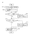
まず、ユーザがコンピュータ1の電源スイッチを押下することによって、情報処理装置1の電源投入を行うと(S201)、情報処理装置1内のMCH20やMAC40などの各コンポーネントへの電源投入、クロック供給、レジスタ値のリセット等の初期化処理が実行される(S202)。MAC40に電源投入されると、各装置間のバスの調整が行われるとともに(S203)、S203と並行してPRS42が起動して、SPD読み出し指示をSPD読み出しシーケンサ122に設定する(S204)。
First, when the user turns on the information processing apparatus 1 by pressing the power switch of the computer 1 (S201), power on each component such as the
SPD読み出しシーケンサ122は、SPD読み出し指示に従って、リードコマンドとSPDアドレスを、SPD読み書き制御部124のレジスタにセットする。SPD読み書き制御部124は、SPD読み出しシーケンサ122からリードコマンドとSPDアドレスを受信すると、シリアルバス制御部146により、シリアルバス90bを介してSPDメモリ60からSPDデータを読み出す(S205)。SPD読み書き制御部124は、SPDメモリ60から読み出したSPDデータを、SPD読み出しレジスタ144を介してSPD記憶部130に格納する(S206)。
The SPD read sequencer 122 sets the read command and the SPD address in the register of the SPD read / write control unit 124 in accordance with the SPD read instruction. When the SPD read / write controller 124 receives the read command and the SPD address from the SPD read sequencer 122, the SPD data is read from the
SPDデータの読み出し処理が行われるのと並行して、各装置間のバスの調整(S203)に続いて、ICH70の給電確認、システムバス設定、ICH70のIOポート有効化、システム設定、ROM80の設定等の情報処理装置1全体としての設定が行われ(S207)、制御レジスタ、トランスレーション・ルックアサイド・バッファ(TLB)、タグの初期化といったプロセッサ10の内部設定が行われる(S208)。このような処理が行われることで、プロセッサ10の命令処理が可能になり、プロセッサ10がメモリ初期化処理を行うためにBIOSを実行する(S209)。
In parallel with the SPD data reading process, the
このとき、SPDデータはS206において、MAC内のSPD記憶部130に格納されている。プロセッサ10は、シリアルバス90bを介することなく、システムバス92a並びにSPD受け渡し部110を介して、SPD記憶部130内にバッファされているSPDデータを読み出して(S210)、図2のフローを終了する。
At this time, the SPD data is stored in the SPD storage unit 130 in the MAC in S206. The
このように、SPD制御装置100への電源投入により、SPDメモリ60からSPDデータの読み出しを開始するため、本実施形態によるSPD制御装置100は、プロセッサ起動後に行われていたSPDデータの読み取り処理を、プロセッサ初期化終了前に開始することができる。また、シリアルバスを用いたSPDデータの読み出し処理を、プロセッサ初期化終了前に終了させることができるため、プロセッサ起動後、SPDデータの読み出し処理を行わずにメモリモジュールの初期化処理を開始して、OS等の立上げ時間を短縮することができる。
As described above, when the
MAC40に接続されるメモリモジュール50の数が増大すると、SPD記憶部130が格納するSPDデータも増大する。また、OS又はFWからのSPD読み出し指示に応答して、SPDメモリ60からの読み出し処理が生じないように、SPD記憶部130には、全てのメモリモジュール50に対応する全SPDデータを格納することが好ましい。そのため、SPD記憶部130は、SPDデータをデータ圧縮してSPDデータに格納し、これにより必要な記憶容量を低減することができる。
When the number of
以下、図3を用いて、SPD記憶部の構成の一例を説明する。
一般的に、システム仕様、又は、システム運用上の制約により、同一チャネルあるいは同一スロットには、同一規格のメモリモジュールが搭載される。そのため、メモリモジュール間におけるSPDデータの内容は、多くの部分が共通であり、一部だけが異なる。SPDデータのデータ圧縮を行うケースでは、そのようなSPDデータの内容の共通性を利用して、SPD記憶部にバッファするSPDデータのデータ圧縮を行う。
Hereinafter, an example of the configuration of the SPD storage unit will be described with reference to FIG.
Generally, memory modules of the same standard are mounted in the same channel or the same slot due to system specifications or restrictions on system operation. For this reason, the contents of the SPD data between the memory modules are common in many parts, and only part of them are different. In the case where data compression of SPD data is performed, data compression of SPD data buffered in the SPD storage unit is performed using such commonality of the contents of SPD data.
図3(a)は、データ圧縮を行わずにSPDデータをSPD記憶部に記憶する場合のSPD記憶部の装置構成の一例を示す図である。図3(a)に示される例では、SPD制御装置100は、SPD記憶部130として、SPD記憶部130aに加えて、有効ポインタ記憶部134aを有する。
図3(a)に示されるように、SPD記憶部130aのSPDアドレス131aは、チャネル番号、スロット番号、SPDメモリのメモリアドレスを有し、これらの組合せにより、メモリモジュール50のSPDデータを特定することができる。このSPDアドレス131aは、読み出し対象の全SPDデータがSPD記憶部130aでヒットするために、全SPDメモリ60の全てのSPDデータを特定するアドレスであることが好ましい。
FIG. 3A is a diagram illustrating an example of a device configuration of the SPD storage unit when SPD data is stored in the SPD storage unit without performing data compression. In the example shown in FIG. 3A, the
As shown in FIG. 3A, the SPD address 131a of the SPD storage unit 130a has a channel number, a slot number, and a memory address of the SPD memory, and the SPD data of the
例えば、SPDメモリ60のメモリ空間は、JEDEC(Joint Electron Devices Engineering Council)から提供される仕様「JEDEC Standard No. 21−C Page 4.1.2.4 -1 Appendix D, Rev. 1.0 : SPD’s for DDR SDRAM」に従って規定される。この場合、SPDメモリ60のメモリ空間は、SPDメモリ60のアドレス数である8ビットの行と、各アドレスに格納されるSPDデータのデータ本体である8ビットの列で規定される。
上記JEDEC仕様に従う場合、図3(a)に示されるメモリ空間は、例えば、チャネル番号(1ビット)+スロット番号(1ビット)+SPDメモリのメモリアドレス(8ビット)の行と、有効ビット(1ビット)+データ本体(8ビット)の列で規定される。つまり、SPDアドレス131aの各アドレスに格納されるデータのフォーマット151は、有効ビット(1ビット)+データ本体(8ビット)のデータ幅を有する。ここで、有効ビット数とは、SPD記憶部130aにSPDメモリ60のSPDアドレスに格納されたデータが格納されたか否かを示すビットである。有効ビットが「1」の場合、SPDデータが格納されており、有効ビットが「0」の場合、SPDデータが格納されていないことを示す。
For example, the memory space of the
In accordance with the JEDEC specification, the memory space shown in FIG. 3A includes, for example, a channel number (1 bit) + slot number (1 bit) + a row of SPD memory address (8 bits) and a valid bit (1 Bit) + data body (8 bits). That is, the
図3(a)のSPDアドレス131aに示すように、SPDアドレス131aは、チャネル番号、スロット番号、SPD内メモリアドレスの並びに従って、昇順でシーケンシャルに配番されている。有効ポインタ記憶部134aは、SPDメモリ60から昇順で読み出されて、SPD記憶部130aにSPDアドレス昇順で格納されたエントリのうち最後尾のSPDアドレスをポインタとして格納する。なお、この最後尾のアドレスを指示するデータを「有効ポインタ」と称する。これにより、有効ポインタは、SPDアドレス131aにおいて、昇順で数えてどの順番のSPDアドレスまでSPDデータが格納されたかを指示する。このように、有効ポインタ記憶部134aはSPDアドレスを格納するために、有効ポインタ記憶部134aは、SPDアドレス131aのアドレス幅と同じ10ビットのデータ幅を有する。
この有効ポインタは、SPDアドレスに従って、SPD記憶部130aにSPDデータを登録するために利用される(後述)。
As shown in the SPD address 131a in FIG. 3A, the SPD address 131a is sequentially allocated in ascending order according to the arrangement of the channel number, slot number, and SPD memory address. The valid
This valid pointer is used to register SPD data in the SPD storage unit 130a according to the SPD address (described later).
図3(b)は、データ圧縮してSPDデータをSPD記憶部に記憶する場合のSPD記憶部の装置構成の一例を示す図である。図3(b)に示される例では、SPD制御装置100は、SPD記憶部130として、SPD記憶部130b、有効ポインタ記憶部134b、SPDポインタ記憶部136b、及びテンポラルポインタ記憶部138bを有する。
FIG. 3B is a diagram illustrating an example of a device configuration of the SPD storage unit when data compression is performed and SPD data is stored in the SPD storage unit. In the example shown in FIG. 3B, the
上記JEDEC仕様によれば、SPDメモリのデータ幅は8ビットであるが、上記仕様に反して、SPDメモリのデータ幅が8ビット以上になる場合がある。例えば、JEDEC仕様の「モジュールデータ幅設定」によれば、メモリモジュールのデータ幅は、2つの8ビットデータを利用してデータ定義される。しかしながら、メモリモジュールの提供会社によっては、上記JEDEC仕様に反して、1つの16ビットデータを利用してモジュールデータ幅を規定したSPDメモリもある。その場合、SPD記憶部130aが、16ビット分のデータ幅を用意する必要がある。 According to the JEDEC specification, the data width of the SPD memory is 8 bits. However, contrary to the specification, the data width of the SPD memory may be 8 bits or more. For example, according to “module data width setting” of the JEDEC specification, the data width of the memory module is defined using two 8-bit data. However, some memory module providers have an SPD memory that defines the module data width using one 16-bit data, contrary to the JEDEC specification. In that case, the SPD storage unit 130a needs to prepare a data width of 16 bits.
図3(b)では、上記のような16ビットのデータ幅を有するSPDデータのデータ圧縮を図るため、SPD記憶部130bには、共通のSPDデータのうち、重複部分を排除してただ1つに選択された固有のSPDデータを格納する。このようなデータ圧縮は、同じ仕様のメモリモジュールを複数使うとき、チャネル番号及びスロット番号が異なるだけで、同じSPDメモリアドレスに格納された同じSPDデータが読み出されるためより有用になる。
SPD記憶部130bの各アドレスに格納されるデータのフォーマット152は、SPDメモリ60に格納されるデータ本体のデータ幅を有する。このデータ本体は、例えば、16ビットである。
また、本実施形態では、SPD記憶部130bは、00〜ffまでのアドレスがあるたため、SPD記憶部130bのアドレス幅は、8ビットである。
In FIG. 3B, in order to compress the data of the SPD data having the 16-bit data width as described above, the SPD storage unit 130b includes only one of the common SPD data by excluding the overlapping portion. The unique SPD data selected is stored. Such data compression is more useful when using a plurality of memory modules having the same specification, because the same SPD data stored in the same SPD memory address is read out only by different channel numbers and slot numbers.
The
In this embodiment, since the SPD storage unit 130b has addresses from 00 to ff, the address width of the SPD storage unit 130b is 8 bits.
SPDポインタ記憶部136bでは、SPD記憶部130a同様に、SPDアドレス131bは、チャネル番号、スロット番号、SPDメモリアドレスを有し、これらの組合せにより、メモリモジュール50のSPDデータを特定する。このSPDアドレス131bは、読み出し対象の全SPDデータがSPD記憶部130bでヒットするために、全SPDメモリ60の全てのSPDデータを特定するアドレスであることが好ましい。
SPDポインタ記憶部136bでは、SPDアドレス131bの各アドレスに格納されるデータのフォーマット153は、有効ビット(1ビット)+SPD記憶部130bのアドレス幅(8ビット)のデータ幅を有する。
In the SPD pointer storage unit 136b, like the SPD storage unit 130a, the SPD address 131b has a channel number, a slot number, and an SPD memory address, and the SPD data of the
In the SPD pointer storage unit 136b, the format 153 of the data stored in each address of the SPD address 131b has a data width of the valid bit (1 bit) + the address width (8 bits) of the SPD storage unit 130b.
有効ポインタ記憶部134bは、SPDメモリ60から昇順で読み出されて、SPDデータの重複部分を排除してSPD記憶部130bにSPDアドレス昇順で格納されたエントリのうち最後尾のSPDアドレスを格納する。この最後尾のSPDアドレスは、有効ポインタは、SPDアドレス131bにおいて、昇順で数えてどの順番のSPDアドレスまでSPDデータが格納されたかを指示する。
なお、有効ポインタ記憶部134bは、SPD記憶部130bのアドレスを格納するためにSPD記憶部130bのアドレス幅と同じ8ビットのデータ幅を有する。有効ポインタは、SPD記憶部130bにSPDデータを登録するために利用される(後述)。
The valid pointer storage unit 134b reads the
The valid pointer storage unit 134b has the same 8-bit data width as the address width of the SPD storage unit 130b in order to store the address of the SPD storage unit 130b. The valid pointer is used to register SPD data in the SPD storage unit 130b (described later).
テンポラルポインタ記憶部138bは、SPDデータの中で重複部分を排除してSPD記憶部130bに固有のSPDデータを選択する処理を行う上で、利用されるSPD記憶部130bのアドレスをテンポラルポインタとして格納する。ここで格納されるSPD記憶部130bのアドレスは、SPD記憶部130bに既に登録されたSPDデータに対応するSPD記憶部130bのアドレスである。このテンポラルポインタ記憶部138bに格納アドレスをインクリメントしながら利用することで、既登録のSPDデータと、SPDメモリ60内のSPDデータとの照合処理を行うことができる。
また、テンポラルポインタ記憶部138bは、SPD記憶部130bのアドレスを格納するために、SPD記憶部130bのアドレス幅と同じ8ビットのデータ幅を有する。
なお、テンポラルポインタ記憶部138bに記憶された情報のより詳細な利用方法は、図5及び6において説明する。
The temporal pointer storage unit 138b stores the address of the SPD storage unit 130b to be used as a temporal pointer in the process of selecting the SPD data unique to the SPD storage unit 130b by eliminating the overlapped portion in the SPD data. To do. The address of the SPD storage unit 130b stored here is the address of the SPD storage unit 130b corresponding to the SPD data already registered in the SPD storage unit 130b. By using the temporal pointer storage unit 138b while incrementing the storage address, it is possible to perform collation processing between the registered SPD data and the SPD data in the
The temporal pointer storage unit 138b has an 8-bit data width that is the same as the address width of the SPD storage unit 130b in order to store the address of the SPD storage unit 130b.
A more detailed usage method of the information stored in the temporal pointer storage unit 138b will be described with reference to FIGS.
SPDメモリ60のデータ幅が16ビットのとき、図3(a)に示すSPD記憶部130aは、全SPDアドレス131a(チャネル・スロット数(4ビット)×SPDメモリアドレス(256ビット))×データ幅(1ビット+16ビット)のメモリ空間を有する。
一方、図3(b)に示すSPDポインタ記憶部136bは、全SPDアドレス131aであるチャネル・スロット数(4ビット)×SPDメモリアドレス(256ビット)×データ幅(9ビット)のメモリ空間を有する。また、SPD記憶部130bは、SPDメモリアドレス(256ビット)×データ幅(16ビット)のメモリ空間を有する。
この場合のデータ圧縮率は、下記式で示される。
図3(b)に示すメモリ容量/図3(a)に示すメモリ容量=(4×256×9+256×16)/(4×256×17)=0.76
したがって、図3(b)に示すメモリ容量は、図3(a)に示すメモリ容量に対して約23〜24%のデータ圧縮効果がある。また、この効果は、チャネル及びスロット数の増加によりさらに大きくなる。例えば、チャネル及びスロット数を32にして、32個の同じメモリモジュールが搭載された場合について考えると、データ圧縮率は、下記式で示される。
When the data width of the
On the other hand, the SPD pointer storage unit 136b shown in FIG. 3B has a memory space of the number of channels / slots (4 bits) × SPD memory address (256 bits) × data width (9 bits) as all SPD addresses 131a. . The SPD storage unit 130b has a memory space of SPD memory address (256 bits) × data width (16 bits).
The data compression rate in this case is shown by the following formula.
Memory capacity shown in FIG. 3B / Memory capacity shown in FIG. 3A = (4 × 256 × 9 + 256 × 16) / (4 × 256 × 17) = 0.76
Therefore, the memory capacity shown in FIG. 3B has a data compression effect of about 23 to 24% with respect to the memory capacity shown in FIG. This effect is further increased by increasing the number of channels and slots. For example, considering the case where 32 identical memory modules are mounted with 32 channels and slots, the data compression rate is expressed by the following equation.
図3(b)に示すメモリ容量/図3(a)に示すメモリ容量=(32×256×9+256×16)/(32×256×17)=0.56
図3(b)に示すメモリ容量は、図3(a)に示すメモリ容量に対して約44%のデータ圧縮効果がある。
また、SPDデータは、そのデータが示す情報は異なっても、同じビット列となる場合がある。このような場合も、重複したSPDデータは排除されてSPD記憶部130bに格納されるため、上記式では表されないデータ圧縮効果がある。
このように、本実施形態では、情報処理装置1に搭載される大量のメモリモジュール用のSPDデータを圧縮して格納することができるため、SPD記憶部130を小型化、低コスト化することができる。
Memory capacity shown in FIG. 3B / Memory capacity shown in FIG. 3A = (32 × 256 × 9 + 256 × 16) / (32 × 256 × 17) = 0.56
The memory capacity shown in FIG. 3B has a data compression effect of about 44% with respect to the memory capacity shown in FIG.
Further, the SPD data may be the same bit string even if the information indicated by the data is different. Even in such a case, since the duplicated SPD data is excluded and stored in the SPD storage unit 130b, there is a data compression effect not represented by the above formula.
Thus, in this embodiment, since a large amount of SPD data for memory modules mounted on the information processing apparatus 1 can be compressed and stored, the SPD storage unit 130 can be reduced in size and cost. it can.
図4を用いて、SPD記憶部130aへのSPDデータの登録フローの一例を説明する。なお、図4に示されたSPDデータの登録フローは、図2で説明した情報処理装置1の起動に伴うSPD読み出し処理(S204〜S206)に行われても良いし、OS又はFWのSPD読み出しに対応するSPDデータがSPD記憶部130に無かった場合に行っても良い。
最初に、SPD読み出しシーケンサ122は、SPD読み書き制御部124に、リードコマンドとSPDアドレスを送出する。SPD読み書き制御部124は、SPD読み出しシーケンサ122からSPDアドレスを受信すると、まず、有効ポインタ記憶部134aの内容を「−1」にリセットする(S301)。
SPD読み書き制御部124は、SPD記憶部130aの内容を全て0にリセットする(S302)。例えば、チャネル番号=0、スロット番号=0、SPD内のオフセット=0に設定する。
An example of the registration flow of SPD data in the SPD storage unit 130a will be described with reference to FIG. Note that the SPD data registration flow shown in FIG. 4 may be performed in the SPD read processing (S204 to S206) accompanying the activation of the information processing apparatus 1 described in FIG. 2, or the OSD or FW SPD read. This may be performed when there is no SPD data corresponding to the in the SPD storage unit 130.
First, the SPD read sequencer 122 sends a read command and an SPD address to the SPD read / write controller 124. When receiving the SPD address from the SPD read sequencer 122, the SPD read / write control unit 124 first resets the contents of the valid
The SPD read / write control unit 124 resets all the contents of the SPD storage unit 130a to 0 (S302). For example, channel number = 0, slot number = 0, and SPD offset = 0 are set.
SPD読み出しシーケンサ122は、読み出し対象となるSPDアドレスが、MAC40に接続されている全てのSPDメモリ60のSPDアドレスの範囲内か否かを判断する(S303)。SPDアドレスは、最初の読み出しの場合、上記したように、チャネル番号=0、スロット番号=0、SPD内のオフセット=0となる。また、S303で判断されるSPDメモリ60のSPDアドレスの範囲は、例えば、チャネル番号0〜4、スロット番号0〜1、SPDメモリのメモリアドレス0〜255である。
読み出し対象のSPDアドレスがSPDアドレス範囲内の場合(S303 Yes)、SPD読み書き制御部124は、SPDメモリ60からSPDデータを読み出して、読み出したSPDデータをSPD読み出しレジスタ144に設定する(S304)。読み出し対象のSPDアドレスがSPDアドレス範囲内にない場合(S303 No)、全SPD範囲内のSPDデータを読み出したと判断して、この処理フローを終了する。
SPD読み書き制御部124は、SPD読み出しレジスタ144に設定されたSPDデータを、SPD記憶部130の該当するSPDアドレス131aに格納する(S305)。次に、SPD読み書き制御部124は、SPD記憶部130に格納したSPDアドレスの先頭ビットを有効(オン)にし、有効ポインタ記憶部134aの有効データ数を1つインクリメントする(S306)。
The SPD read sequencer 122 determines whether the SPD address to be read is within the range of the SPD addresses of all the
When the SPD address to be read is within the SPD address range (S303 Yes), the SPD read / write controller 124 reads the SPD data from the
The SPD read / write control unit 124 stores the SPD data set in the SPD read
SPD読み出しシーケンサ122は、有効ポインタ記憶部134aに格納した有効データ数が、S303で取得したSPDアドレス範囲内の最終SPDアドレスに相当しないと判断する場合(S307 No)はS308に進む。一方、有効ポインタ記憶部134aに格納した有効データ数がSPDアドレス範囲内の最終SPDアドレスに相当すると判断する場合(S307 Yes)、全SPD範囲内のSPDデータを読み出したと判断して、フローを終了する。
S308では、SPD読み書き制御部124は、読み出し対象のSPDアドレスをインクリメントして、S303に戻り、上記したステップS303〜S307の処理を再度繰り返すことで、SPDデータをさらに読み出す。
If the SPD read sequencer 122 determines that the number of valid data stored in the valid
In S308, the SPD read / write controller 124 increments the SPD address to be read, returns to S303, and repeats the processes in steps S303 to S307 described above to further read SPD data.
図5及び6を用いて、SPD記憶部130bのSPDデータの登録フローの一例を説明する。
図5の登録フローのS301〜S303は、図4を用いて説明した登録フローS301〜S303と同じ処理が行われる。
S303に続き、SPD読み書き制御部124は、テンポラルポインタ記憶部138bを「0」にリセットする(S401)。SPD読み書き制御部124は、受信したリードコマンドとSPDアドレスに従ってSPDメモリ60からSPDデータを読み出し(S402)、読み出したSPDデータを、SPD読み出しレジスタ144に設定する(S403)。
SPD読み出しシーケンサ122は、有効ポインタ記憶部134bと、テンポラルポインタ記憶部138bとを比較する(S404)。有効ポインタ記憶部134bに設定された有効データ数が、テンポラルポインタ記憶部138bに設定されたデータ数以上の場合(S404 No)、新たにSPDデータ記憶部130bにSPDデータを登録するために、S405に進む。一方、有効ポインタ記憶部134bに設定された有効データ数が、テンポラルポインタ記憶部138bに設定されたデータ数以下の場合(S404 Yes)、新たにSPDポインタ記憶部136bにSPDデータ記憶部130bのアドレスを登録するために、S410に進む。
An example of an SPD data registration flow in the SPD storage unit 130b will be described with reference to FIGS.
In S301 to S303 of the registration flow of FIG. 5, the same processing as the registration flows S301 to S303 described with reference to FIG. 4 is performed.
Subsequent to S303, the SPD read / write control unit 124 resets the temporal pointer storage unit 138b to “0” (S401). The SPD read / write controller 124 reads SPD data from the
The SPD read sequencer 122 compares the valid pointer storage unit 134b with the temporal pointer storage unit 138b (S404). If the number of valid data set in the valid pointer storage unit 134b is greater than or equal to the number of data set in the temporal pointer storage unit 138b (No in S404), in order to newly register SPD data in the SPD data storage unit 130b, S405 Proceed to On the other hand, when the number of valid data set in the valid pointer storage unit 134b is equal to or less than the number of data set in the temporal pointer storage unit 138b (Yes in S404), the address of the SPD data storage unit 130b is newly stored in the SPD pointer storage unit 136b. To register S <b> 410, the process proceeds to S <b> 410.
S405〜S409では、SPD読み書き制御部124によるSPDポインタ記憶部136bへのSPD記憶部130bのアドレス登録処理が行われる。 In S405 to S409, the SPD read / write control unit 124 performs address registration processing of the SPD storage unit 130b in the SPD pointer storage unit 136b.
まず、SPD読み書き制御部124は、SPD記憶部130bの有効データ数が増加するため、有効ポインタ記憶部134bの有効ポインタがインクリメントする(S405)。
SPD読み書き制御部124は、有効ポインタ記憶部134bの有効ポインタと同じ値をとるSPD記憶部130bのアドレスに、S402で読み出したSPDデータを登録する(S406)。有効ポインタ記憶部134bは、SPD記憶部130bの有効データ数を指示するため、新たにSPD記憶部130bにSPDデータを登録するときは、S405でインクリメントされた有効ポインタが利用される。
次に、S406で新たにSPDデータが登録されたため、登録されたSPDデータを指示するSPD記憶部130bのアドレスを、SPD読み書き制御部124は、SPDポインタ記憶部136bに登録する(S407)。
SPD読み出しシーケンサ122は、有効ポインタが、SPD記憶部130bの最終アドレスより大きいか否かを判断することにより、SPDアドレスが最終アドレスに達したか否かを判断する(S408)。有効ポインタが最終アドレスより(S408 Yes)、SPD記憶部130bは全アドレスにSDP情報が格納されているため、フローを終了する。有効ポインタが最終アドレスより小さい場合(S408 No)、まだSPD記憶部130bにSPDデータを格納できるため、読み出しSPDアドレスをインクリメントして(S409)、S303に戻り再度処理を繰り返す。有効ポインタが最終アドレスと同じ場合(S408 Yes)、SPDアドレスが最終アドレスに達したと判断して、フロー処理を終了する。
First, since the number of valid data in the SPD storage unit 130b increases, the SPD read / write control unit 124 increments the valid pointer in the valid pointer storage unit 134b (S405).
The SPD read / write control unit 124 registers the SPD data read in S402 at the address of the SPD storage unit 130b that takes the same value as the valid pointer of the valid pointer storage unit 134b (S406). Since the valid pointer storage unit 134b indicates the number of valid data in the SPD storage unit 130b, when the SPD data is newly registered in the SPD storage unit 130b, the valid pointer incremented in S405 is used.
Next, since the SPD data is newly registered in S406, the SPD read / write control unit 124 registers the address of the SPD storage unit 130b instructing the registered SPD data in the SPD pointer storage unit 136b (S407).
The SPD read sequencer 122 determines whether the SPD address has reached the final address by determining whether the valid pointer is larger than the final address of the SPD storage unit 130b (S408). Since the valid pointer is from the last address (S408 Yes), the SPD storage unit 130b ends the flow because SDP information is stored in all addresses. If the valid pointer is smaller than the final address (No in S408), since the SPD data can still be stored in the SPD storage unit 130b, the read SPD address is incremented (S409), and the process returns to S303 and is repeated again. If the valid pointer is the same as the final address (S408 Yes), it is determined that the SPD address has reached the final address, and the flow process ends.
S410では、テンポラルポインタ記憶部138bのテンポラルポインタが指示するSPD記憶部130bのSPDデータと、S403でSPD読み出しレジスタ144に格納されるSPDデータが一致するか否かを判断する(S410)。一致する場合(S410 Yes)は、有効ポインタ記憶部136bにテンポラルポインタを記録する(S411)。S411に続き、S412では、次のSPDアドレスについて処理をすすめるために、読み出しSPDアドレスをインクリメントする。一致しない場合(S410 No)は、SPDデータ登録部130bの次の有効データを参照するためにテンポラルポインタをインクリメントする(S413)。
In S410, it is determined whether the SPD data in the SPD storage unit 130b indicated by the temporal pointer in the temporal pointer storage unit 138b matches the SPD data stored in the SPD read
図7を用いて、FW又はOSからの読み出しによるSPD記憶部130aからのSPDデータの読み出しフローの一例を説明する。
最初に、SPD受け渡し部110は、FW又はOSからの読み出し要求と共にこの読み出し要求に含まれる読み出し対象のSPDアドレスを受信する(S501)。読み出し対象となるSPDアドレスは、特定のメモリモジュールの全SPDアドレスや、全メモリモジュールの全SPDアドレス等である。SPD読み書き制御部124は、全SPDアドレス131aを、SPD記憶部130aから読み出す(S502)。
SPD読み出しシーケンサは、S501で受信した読み出しアドレスが、S502で読み出した全SPDアドレス131aの範囲内にあるか否かを判断する(S503)。読み出し対象のSPDアドレスが、有効なSPDアドレス範囲内に無い場合(S503 No)、図3のS304〜S305で説明したようにSPDメモリ60からSPD仕様情報を読み出す処理を実行して(S506)、読み出し対象のSPDアドレスにあるSPDデータを、SPD記憶部130a又は130bに格納し、S504に進む。
なお、このようにFW又はOSから受信した読み出し対象となるSPDデータが、SPD記憶部130aに無い状況は、図2で説明したようなプロセッサ初期化前のSPDデータの読み出し処理を無効化したケースが該当する。S503及びS506はそのような場合の異常処理として機能し得る。
また、S503において有効なSPDアドレス範囲内にある場合(S503 Yes)、S504に進む。
An example of the flow of reading SPD data from the SPD storage unit 130a by reading from the FW or OS will be described with reference to FIG.
First, the
The SPD read sequencer determines whether or not the read address received in S501 is within the range of all SPD addresses 131a read in S502 (S503). When the SPD address to be read is not within the valid SPD address range (No in S503), the process of reading SPD specification information from the
It should be noted that the situation in which the SPD data to be read received from the FW or OS is not in the SPD storage unit 130a as described above is a case where the SPD data read processing before processor initialization as described in FIG. 2 is invalidated. Is applicable. S503 and S506 can function as abnormality processing in such a case.
If it is within the valid SPD address range in S503 (S503 Yes), the process proceeds to S504.
S504では、読み出したSPDデータが有効か否かを判断する。なお、SPD記憶部130aに「−1」が入力されているため、その値に基づいてSPDデータが有効か否かを判断することができる。SPDデータが有効でない場合(S504 No)は、S507に進み再度SPDデータをSPDから取得する。なお、S507では、図3のS304〜S305で説明したようにSPDメモリ60からSPD仕様情報を読み出す処理を実行する(S507)。読み出し処理終了後、S505に進む。SPDデータが有効である場合(S504 Yes)は、読み出したSPDデータをSPD受け渡し部110を介して要求元であるFW又はOSに戻して(S505)、SPDデータの読み出しフローを終了する。
In S504, it is determined whether or not the read SPD data is valid. Since “−1” is input to the SPD storage unit 130a, it can be determined whether the SPD data is valid based on the value. When the SPD data is not valid (No in S504), the process proceeds to S507 and the SPD data is acquired again from the SPD. In S507, as described in S304 to S305 in FIG. 3, a process of reading SPD specification information from the
図8を用いて、FW又はOSからの読み出しによるSPD記憶部130bからのSPDデータの読み出しフローの一例を説明する。
最初に、SPD読み書き制御部124は、FW又はOSからの読み出し要求と共に読み出し要求に含まれる読み出し対象のSPDアドレスを受信する(S601)。SPD読み書き制御部124は、読み出し対象のSPDアドレスに格納されるポインタをSPD記憶部130aから読み出す(S602)。SPD読み書き制御部124は、読み出したポインタが有効か否かを判断する(S603)。言い換えれば、SPD読み書き制御部124は、SPDポインタ記憶部136bの中で受信した読み出し対象のSPDアドレス131bのポインタの有効ビットが「1」か「0」かを判断する。有効ビットが「0」の場合は、当該データエントリにはSPD記憶部130bのアドレスが格納されない。ポインタが有効でない場合(S603 No)は、SPDデータのSPD記憶部130bへの登録処理が実行される。この処理では、SPD読み書き制御部124は、有効ポインタ記憶部134bから有効ポインタを取得する(S606)。そして、図5のS303、S401〜S413の処理を実行して、SPDメモリからSPDデータを読み出して、SPD記憶部130bにSPDデータを登録する(S607)。SPD読み出し処理終了後、S604に進む。
一方、S603で、ポインタが有効であると判断された場合(S603 Yes)は、SPDポインタ記憶部136bに格納されるSPD記憶部130bのアドレスを参照して、SPD記憶部130bからSPDデータを読み出す(S604)。
SPD読み書き制御部124は、読み出したSPDデータを、SPD受け渡し部110を介して要求元であるFW又はOSに戻して(S605)、SPDデータの読み出しフローを終了する。
An example of the flow of reading SPD data from the SPD storage unit 130b by reading from the FW or OS will be described with reference to FIG.
First, the SPD read / write controller 124 receives the SPD address to be read included in the read request together with the read request from the FW or the OS (S601). The SPD read / write controller 124 reads the pointer stored at the SPD address to be read from the SPD storage unit 130a (S602). The SPD read / write controller 124 determines whether or not the read pointer is valid (S603). In other words, the SPD read / write control unit 124 determines whether the valid bit of the pointer of the SPD address 131b to be read received in the SPD pointer storage unit 136b is “1” or “0”. When the valid bit is “0”, the address of the SPD storage unit 130b is not stored in the data entry. If the pointer is not valid (No in S603), the SPD data is registered in the SPD storage unit 130b. In this process, the SPD read / write control unit 124 acquires a valid pointer from the valid pointer storage unit 134b (S606). Then, the processes of S303 and S401 to S413 in FIG. 5 are executed to read the SPD data from the SPD memory and register the SPD data in the SPD storage unit 130b (S607). After the SPD read process is completed, the process proceeds to S604.
On the other hand, if it is determined in S603 that the pointer is valid (S603 Yes), the SPD data is read from the SPD storage unit 130b with reference to the address of the SPD storage unit 130b stored in the SPD pointer storage unit 136b. (S604).
The SPD read / write control unit 124 returns the read SPD data to the requesting FW or OS via the SPD transfer unit 110 (S605), and ends the SPD data read flow.
以上述べた一実施形態は、以下の付記の通りである。
(付記1)
プロセッサ、メモリモジュール、及び該メモリモジュールの仕様を示す仕様情報を記憶する仕様情報記憶メモリに接続される制御装置であって、
前記制御装置への電源投入により、前記仕様情報記憶メモリから前記仕様情報を読み出す読み出し部と、
前記仕様情報記憶メモリから読み出された仕様情報を格納する記憶部と、
前記プロセッサから前記仕様情報の読み出し指示を受信して、前記記憶部に格納された前記仕様情報を前記プロセッサに受け渡す受け渡し部と、
を有することを特徴とする制御装置。
(付記2)
前記制御装置は、複数のメモリモジュールと、該複数のメモリモジュールにそれぞれ対応する複数の前記仕様情報記憶メモリとに接続され、
前記記憶部は、前記複数の仕様情報記憶メモリに格納される複数の前記仕様情報のうち、重複部分を取り除いた仕様情報を格納し、
前記制御装置は、前記記憶部のアドレスを指示するポインタ情報を、前記メモリモジュールの位置情報と関連付けて格納するポインタ記憶部をさらに有し、
前記SPD読み出し部は、読み出し対象となるメモリモジュールの位置情報を含む仕様情報の読み出し指示を受信して、該メモリモジュールの位置情報に関連付けられる前記ポインタ情報を前記ポインタ記憶部から取得し、且つ、該取得した前記ポインタ情報によって指示される前記記憶部のアドレスから、前記仕様情報を取得することを特徴とする、付記1に記載の制御装置。
(付記3)
前記読み出し部は、前記仕様情報をバースト転送で前記プロセッサに受け渡すことを特徴とする、付記1又は2に記載の制御装置。
(付記4)
プロセッサと、
メモリモジュールと、
制御装置と、を備え、
前記メモリモジュールは、
第一のメモリと、
前記メモリモジュールの仕様を示す仕様情報を記憶する第二のメモリとを有し、
前記制御装置は、
前記制御装置への電源投入により、前記第二のメモリから前記仕様情報を読み出す読み出し部と、
前記読出し部が読みだした仕様情報を格納する記憶部と、
前記プロセッサからの読み出し指示を受信して、前記記憶部に格納された仕様情報を前記プロセッサに受け渡す受け渡し部と、
を有することを特徴とする情報処理装置。
(付記5)
前記制御装置は、前記メモリモジュールへのアクセスを制御するメモリ制御装置であることを特徴とする、付記4に記載の情報処理装置。
(付記6)
前記制御装置は、複数のメモリモジュールと、該複数のメモリモジュールにそれぞれ対応する複数の前記仕様情報記憶メモリとに接続され、
前記記憶部は、前記複数の仕様情報記憶メモリに格納される複数の前記仕様情報のうち、重複部分を取り除いた仕様情報を格納し、
前記制御装置は、前記記憶部のアドレスを指示するポインタ情報を、前記メモリモジュールの位置情報と関連付けて格納するポインタ記憶部をさらに有し、
前記SPD読み出し部は、読み出し対象となるメモリモジュールの位置情報を含む仕様情報の読み出し指示を受信して、該メモリモジュールの位置情報に関連付けられる前記ポインタ情報を前記ポインタ記憶部から取得し、且つ、該取得した前記ポインタ情報によって指示される前記記憶部のアドレスから、前記仕様情報を取得することを特徴とする、付記4又は5に記載の情報処理装置。
(付記7)
前記読み出し部は、前記仕様情報をバースト転送で前記プロセッサに受け渡すことを特徴とする、付記4〜6のいずれか1項に記載の情報処理装置。
(付記8)
プロセッサ、メモリモジュール、及び該メモリモジュールの仕様を示す仕様情報を記憶する仕様情報記憶メモリに接続され、且つ記憶部を有する制御装置により前記プロセッサに前記メモリモジュールを認識させるメモリモジュール認識方法であって、
前記プロセッサが、前記制御装置への電源投入により、立ち上げ処理を開始し、
前記制御装置は、前記制御装置への電源投入により、前記仕様情報記憶メモリから前記仕様情報の読み出しを開始し、
前記制御装置は、前記仕様情報を前記記憶部に格納し、
前記制御装置は、前記立ち上げ処理を終了したプロセッサから前記仕様情報の読み出し指示を受信して、前記記憶部に格納された前記仕様情報を前記プロセッサに受け渡すことを特徴とするメモリモジュール認識方法。
(付記9)
前記制御装置は、複数のメモリモジュールと、該複数のメモリモジュールにそれぞれ対応する複数の前記仕様情報記憶メモリとに接続され、且つ、ポインタ記憶部をさらに有すると共に、
前記複数の仕様情報記憶メモリに格納される複数の前記仕様情報のうち、重複部分を取り除いた仕様情報を前記記憶部に格納し、
前記記憶部のアドレスを指示するポインタ情報を、前記メモリモジュールの位置情報と関連付けて前記ポインタ記憶部に格納し、
読み出し対象となるメモリモジュールの位置情報を含む仕様情報の読み出し指示を受信して、該メモリモジュールの位置情報に関連付けられる前記ポインタ情報を前記ポインタ記憶部から取得し、且つ、該取得した前記ポインタ情報によって指示される前記記憶部のアドレスから、前記仕様情報を取得することを特徴とする、付記8に記載のメモリモジュール認識方法。
(付記10)
前記仕様情報をバースト転送で前記プロセッサに受け渡すステップをさらに有することを特徴とする、付記8又は9に記載のメモリモジュール認識方法。
(付記11)
前記制御装置は、複数のメモリモジュール及び前記プロセッサとシステムバスで接続され、
前記制御装置は、前記複数のメモリモジュールにそれぞれ対応する複数の前記仕様情報記憶メモリとシリアルバスで接続され、
前記仕様情報の読み出しを開始するステップは、前記シリアルバスを介して実行され、
前仕様情報の受け渡しステップは、前記システムバスを介して実行されることを特徴とする、付記8〜10のいずれか1項に記載のメモリモジュール認識方法。
One embodiment described above is as follows.
(Appendix 1)
A control device connected to a processor, a memory module, and a specification information storage memory for storing specification information indicating specifications of the memory module,
A reading unit that reads the specification information from the specification information storage memory by turning on the power to the control device;
A storage unit for storing specification information read from the specification information storage memory;
A delivery unit that receives an instruction to read the specification information from the processor, and delivers the specification information stored in the storage unit to the processor;
A control device comprising:
(Appendix 2)
The control device is connected to a plurality of memory modules and a plurality of the specification information storage memories respectively corresponding to the plurality of memory modules,
The storage unit stores the specification information from which the overlapping portion is removed among the plurality of specification information stored in the plurality of specification information storage memories,
The control device further includes a pointer storage unit that stores pointer information indicating an address of the storage unit in association with position information of the memory module;
The SPD reading unit receives an instruction to read specification information including position information of a memory module to be read, acquires the pointer information associated with the position information of the memory module from the pointer storage unit, and The control device according to appendix 1, wherein the specification information is acquired from an address of the storage unit indicated by the acquired pointer information.
(Appendix 3)
The control device according to appendix 1 or 2, wherein the reading unit transfers the specification information to the processor by burst transfer.
(Appendix 4)
A processor;
A memory module;
A control device,
The memory module is
The first memory,
A second memory for storing specification information indicating the specification of the memory module;
The control device includes:
A reading unit that reads the specification information from the second memory by turning on the power to the control device;
A storage unit for storing specification information read by the reading unit;
A delivery unit that receives a read instruction from the processor and delivers the specification information stored in the storage unit to the processor;
An information processing apparatus comprising:
(Appendix 5)
The information processing apparatus according to appendix 4, wherein the control apparatus is a memory control apparatus that controls access to the memory module.
(Appendix 6)
The control device is connected to a plurality of memory modules and a plurality of the specification information storage memories respectively corresponding to the plurality of memory modules,
The storage unit stores the specification information from which the overlapping portion is removed among the plurality of specification information stored in the plurality of specification information storage memories,
The control device further includes a pointer storage unit that stores pointer information indicating an address of the storage unit in association with position information of the memory module;
The SPD reading unit receives an instruction to read specification information including position information of a memory module to be read, acquires the pointer information associated with the position information of the memory module from the pointer storage unit, and 6. The information processing apparatus according to appendix 4 or 5, wherein the specification information is acquired from an address of the storage unit indicated by the acquired pointer information.
(Appendix 7)
The information processing apparatus according to any one of appendices 4 to 6, wherein the reading unit delivers the specification information to the processor by burst transfer.
(Appendix 8)
A memory module recognition method connected to a processor, a memory module, and a specification information storage memory for storing specification information indicating the specification of the memory module, and causing the processor to recognize the memory module by a control device having a storage unit. ,
The processor starts a startup process by turning on the power to the control device,
The control device starts reading the specification information from the specification information storage memory by turning on the power to the control device,
The control device stores the specification information in the storage unit,
The control device receives an instruction to read the specification information from a processor that has finished the start-up process, and delivers the specification information stored in the storage unit to the processor .
(Appendix 9)
The control device is connected to a plurality of memory modules and a plurality of the specification information storage memories respectively corresponding to the plurality of memory modules, and further includes a pointer storage unit,
Among the plurality of specification information stored in the plurality of specification information storage memories, storing the specification information in which the overlapping portion is removed, in the storage unit,
Pointer information indicating the address of the storage unit is stored in the pointer storage unit in association with the position information of the memory module;
A specification information read instruction including the position information of the memory module to be read is received, the pointer information associated with the position information of the memory module is acquired from the pointer storage unit, and the acquired pointer information 9. The memory module recognition method according to appendix 8, wherein the specification information is acquired from an address of the storage unit indicated by
(Appendix 10)
10. The memory module recognition method according to appendix 8 or 9, further comprising a step of transferring the specification information to the processor by burst transfer.
(Appendix 11)
The control device is connected to a plurality of memory modules and the processor via a system bus,
The control device is connected to a plurality of the specification information storage memories respectively corresponding to the plurality of memory modules through a serial bus,
The step of starting the reading of the specification information is executed via the serial bus,
The memory module recognition method according to any one of appendices 8 to 10, wherein the step of transferring the pre-specification information is executed via the system bus.
1 情報処理装置
10 プロセッサ
40 MAC
42 PRS
50 メモリモジュール
60 SPDメモリ
100 SPD制御装置
110 SPD受け渡し部
120 SPD読み出し部
122 SPD読み出しシーケンサ
124 SPD読み出しレジスタ
130、130a、130b SPD記憶部
1
42 PRS
DESCRIPTION OF
Claims (10)
前記制御装置への電源投入により、前記仕様情報記憶メモリから前記仕様情報を読み出す読み出し部と、
前記仕様情報記憶メモリから読み出された仕様情報を格納する記憶部と、
前記プロセッサから前記仕様情報の読み出し指示を受信して、前記記憶部に格納された前記仕様情報を前記プロセッサに受け渡す受け渡し部と、
を有することを特徴とする制御装置。 A control device connected to a processor, a memory module, and a specification information storage memory for storing specification information indicating specifications of the memory module,
A reading unit that reads the specification information from the specification information storage memory by turning on the power to the control device;
A storage unit for storing specification information read from the specification information storage memory;
A delivery unit that receives an instruction to read the specification information from the processor, and delivers the specification information stored in the storage unit to the processor;
A control device comprising:
前記記憶部は、前記複数の仕様情報記憶メモリに格納される複数の前記仕様情報のうち、重複部分を取り除いた仕様情報を格納し、
前記制御装置は、前記記憶部のアドレスを指示するポインタ情報を、前記メモリモジュールの位置情報と関連付けて格納するポインタ記憶部をさらに有し、
前記SPD読み出し部は、読み出し対象となるメモリモジュールの位置情報を含む仕様情報の読み出し指示を受信して、該メモリモジュールの位置情報に関連付けられる前記ポインタ情報を前記ポインタ記憶部から取得し、且つ、該取得した前記ポインタ情報によって指示される前記記憶部のアドレスから、前記仕様情報を取得することを特徴とする、請求項1に記載の制御装置。 The control device is connected to a plurality of memory modules and a plurality of the specification information storage memories respectively corresponding to the plurality of memory modules,
The storage unit stores the specification information from which the overlapping portion is removed among the plurality of specification information stored in the plurality of specification information storage memories,
The control device further includes a pointer storage unit that stores pointer information indicating an address of the storage unit in association with position information of the memory module;
The SPD reading unit receives an instruction to read specification information including position information of a memory module to be read, acquires the pointer information associated with the position information of the memory module from the pointer storage unit, and The control device according to claim 1, wherein the specification information is acquired from an address of the storage unit indicated by the acquired pointer information.
メモリモジュールと、
制御装置と、を備え、
前記メモリモジュールは、
第一のメモリと、
前記メモリモジュールの仕様を示す仕様情報を記憶する第二のメモリとを有し、
前記制御装置は、
前記制御装置への電源投入により、前記第二のメモリから前記仕様情報を読み出す読み出し部と、
前記読出し部が読みだした仕様情報を格納する記憶部と、
前記プロセッサからの読み出し指示を受信して、前記記憶部に格納された仕様情報を前記プロセッサに受け渡す受け渡し部と、
を有することを特徴とする情報処理装置。 A processor;
A memory module;
A control device,
The memory module is
The first memory,
A second memory for storing specification information indicating the specification of the memory module;
The control device includes:
A reading unit that reads the specification information from the second memory by turning on the power to the control device;
A storage unit for storing specification information read by the reading unit;
A delivery unit that receives a read instruction from the processor and delivers the specification information stored in the storage unit to the processor;
An information processing apparatus comprising:
前記記憶部は、前記複数の仕様情報記憶メモリに格納される複数の前記仕様情報のうち、重複部分を取り除いた仕様情報を格納し、
前記制御装置は、前記記憶部のアドレスを指示するポインタ情報を、前記メモリモジュールの位置情報と関連付けて格納するポインタ記憶部をさらに有し、
前記SPD読み出し部は、読み出し対象となるメモリモジュールの位置情報を含む仕様情報の読み出し指示を受信して、該メモリモジュールの位置情報に関連付けられる前記ポインタ情報を前記ポインタ記憶部から取得し、且つ、該取得した前記ポインタ情報によって指示される前記記憶部のアドレスから、前記仕様情報を取得することを特徴とする、請求項4又は5に記載の情報処理装置。 The control device is connected to a plurality of memory modules and a plurality of the specification information storage memories respectively corresponding to the plurality of memory modules,
The storage unit stores the specification information from which the overlapping portion is removed among the plurality of specification information stored in the plurality of specification information storage memories,
The control device further includes a pointer storage unit that stores pointer information indicating an address of the storage unit in association with position information of the memory module;
The SPD reading unit receives an instruction to read specification information including position information of a memory module to be read, acquires the pointer information associated with the position information of the memory module from the pointer storage unit, and The information processing apparatus according to claim 4, wherein the specification information is acquired from an address of the storage unit indicated by the acquired pointer information.
前記プロセッサが、前記制御装置への電源投入により、立ち上げ処理を開始し、
前記制御装置は、前記制御装置への電源投入により、前記仕様情報記憶メモリから前記仕様情報の読み出しを開始し、
前記制御装置は、前記仕様情報を前記記憶部に格納し、
前記制御装置は、前記立ち上げ処理を終了したプロセッサから前記仕様情報の読み出し指示を受信して、前記記憶部に格納された前記仕様情報を前記プロセッサに受け渡すことを特徴とするメモリモジュール認識方法。 A memory module recognition method connected to a processor, a memory module, and a specification information storage memory for storing specification information indicating the specification of the memory module, and causing the processor to recognize the memory module by a control device having a storage unit. ,
The processor starts a startup process by turning on the power to the control device,
The control device starts reading the specification information from the specification information storage memory by turning on the power to the control device,
The control device stores the specification information in the storage unit,
The control device receives an instruction to read the specification information from a processor that has finished the start-up process, and delivers the specification information stored in the storage unit to the processor .
前記複数の仕様情報記憶メモリに格納される複数の前記仕様情報のうち、重複部分を取り除いた仕様情報を前記記憶部に格納し、
前記記憶部のアドレスを指示するポインタ情報を、前記メモリモジュールの位置情報と関連付けて前記ポインタ記憶部に格納し、
読み出し対象となるメモリモジュールの位置情報を含む仕様情報の読み出し指示を受信して、該メモリモジュールの位置情報に関連付けられる前記ポインタ情報を前記ポインタ記憶部から取得し、且つ、該取得した前記ポインタ情報によって指示される前記記憶部のアドレスから、前記仕様情報を取得することを特徴とする、請求項8に記載のメモリモジュール認識方法。 The control device is connected to a plurality of memory modules and a plurality of the specification information storage memories respectively corresponding to the plurality of memory modules, and further includes a pointer storage unit,
Among the plurality of specification information stored in the plurality of specification information storage memories, storing the specification information in which the overlapping portion is removed, in the storage unit,
Pointer information indicating the address of the storage unit is stored in the pointer storage unit in association with the position information of the memory module;
A specification information read instruction including the position information of the memory module to be read is received, the pointer information associated with the position information of the memory module is acquired from the pointer storage unit, and the acquired pointer information The memory module recognition method according to claim 8, wherein the specification information is acquired from an address of the storage unit indicated by.
Priority Applications (2)
| Application Number | Priority Date | Filing Date | Title |
|---|---|---|---|
| JP2008200051A JP5292978B2 (en) | 2008-08-01 | 2008-08-01 | Control apparatus, information processing apparatus, and memory module recognition method |
| US12/474,857 US8301858B2 (en) | 2008-08-01 | 2009-05-29 | Control device |
Applications Claiming Priority (1)
| Application Number | Priority Date | Filing Date | Title |
|---|---|---|---|
| JP2008200051A JP5292978B2 (en) | 2008-08-01 | 2008-08-01 | Control apparatus, information processing apparatus, and memory module recognition method |
Publications (2)
| Publication Number | Publication Date |
|---|---|
| JP2010039645A true JP2010039645A (en) | 2010-02-18 |
| JP5292978B2 JP5292978B2 (en) | 2013-09-18 |
Family
ID=41609496
Family Applications (1)
| Application Number | Title | Priority Date | Filing Date |
|---|---|---|---|
| JP2008200051A Expired - Fee Related JP5292978B2 (en) | 2008-08-01 | 2008-08-01 | Control apparatus, information processing apparatus, and memory module recognition method |
Country Status (2)
| Country | Link |
|---|---|
| US (1) | US8301858B2 (en) |
| JP (1) | JP5292978B2 (en) |
Cited By (4)
| Publication number | Priority date | Publication date | Assignee | Title |
|---|---|---|---|---|
| JP2011175577A (en) * | 2010-02-25 | 2011-09-08 | Nec Computertechno Ltd | Computer system, memory initialization method, and program |
| JP2011233006A (en) * | 2010-04-28 | 2011-11-17 | Brother Ind Ltd | Electronic circuit, image-forming apparatus and initialization method for ddr-sdram |
| WO2011148484A1 (en) * | 2010-05-27 | 2011-12-01 | 富士通株式会社 | Memory system, memory device, and memory interface device |
| US10109258B2 (en) | 2013-07-18 | 2018-10-23 | Mitsubishi Electric Corporation | Device and method for presenting information according to a determined recognition degree |
Families Citing this family (7)
| Publication number | Priority date | Publication date | Assignee | Title |
|---|---|---|---|---|
| US8977831B2 (en) * | 2009-02-11 | 2015-03-10 | Stec, Inc. | Flash backed DRAM module storing parameter information of the DRAM module in the flash |
| JP6000655B2 (en) * | 2012-05-30 | 2016-10-05 | キヤノン株式会社 | Information processing apparatus, information processing apparatus control method, and program |
| US20130346735A1 (en) * | 2012-06-21 | 2013-12-26 | Ati Technologies Ulc | Enhanced system management bus |
| US8990479B2 (en) * | 2012-07-30 | 2015-03-24 | Lenovo Enterprise Solutions (Singapore) Pte. Ltd. | Using persistent memory regions within memory devices to collect serial presence detect and performance data |
| KR101987426B1 (en) * | 2012-09-07 | 2019-09-30 | 삼성전자주식회사 | Nonvolatile memory module, memory system including nonvolatile memory module and controlling method of nonvolatile memory module |
| US9483411B2 (en) * | 2014-03-05 | 2016-11-01 | Kabushiki Kaisha Toshiba | Memory system which transfers management information between first and second memories in a burst mode before a read process is performed on a third memory |
| CN115686164A (en) * | 2021-07-26 | 2023-02-03 | 瑞昱半导体股份有限公司 | Power supply terminal device, power supply system and non-transitory computer readable medium |
Citations (3)
| Publication number | Priority date | Publication date | Assignee | Title |
|---|---|---|---|---|
| JPH05289935A (en) * | 1992-04-06 | 1993-11-05 | Hitachi Ltd | Storage device |
| JP2006127515A (en) * | 2004-10-25 | 2006-05-18 | Samsung Electronics Co Ltd | Memory system controlling interface timing in memory module and timing control method |
| JP2007122627A (en) * | 2005-10-31 | 2007-05-17 | Toshiba Corp | Information processor and memory initialization method |
Family Cites Families (4)
| Publication number | Priority date | Publication date | Assignee | Title |
|---|---|---|---|---|
| US7340561B2 (en) * | 2004-01-08 | 2008-03-04 | Hewlett-Packard Development Company, L.P. | Computer memory initialization |
| JP4616586B2 (en) * | 2004-06-30 | 2011-01-19 | 富士通株式会社 | Memory initialization controller |
| US20060064563A1 (en) * | 2004-09-23 | 2006-03-23 | Hobson Louis B | Caching presence detection data |
| KR100777446B1 (en) * | 2005-05-25 | 2007-11-21 | 삼성전자주식회사 | Electronic device and booting method thereof |
-
2008
- 2008-08-01 JP JP2008200051A patent/JP5292978B2/en not_active Expired - Fee Related
-
2009
- 2009-05-29 US US12/474,857 patent/US8301858B2/en not_active Expired - Fee Related
Patent Citations (3)
| Publication number | Priority date | Publication date | Assignee | Title |
|---|---|---|---|---|
| JPH05289935A (en) * | 1992-04-06 | 1993-11-05 | Hitachi Ltd | Storage device |
| JP2006127515A (en) * | 2004-10-25 | 2006-05-18 | Samsung Electronics Co Ltd | Memory system controlling interface timing in memory module and timing control method |
| JP2007122627A (en) * | 2005-10-31 | 2007-05-17 | Toshiba Corp | Information processor and memory initialization method |
Cited By (5)
| Publication number | Priority date | Publication date | Assignee | Title |
|---|---|---|---|---|
| JP2011175577A (en) * | 2010-02-25 | 2011-09-08 | Nec Computertechno Ltd | Computer system, memory initialization method, and program |
| JP2011233006A (en) * | 2010-04-28 | 2011-11-17 | Brother Ind Ltd | Electronic circuit, image-forming apparatus and initialization method for ddr-sdram |
| WO2011148484A1 (en) * | 2010-05-27 | 2011-12-01 | 富士通株式会社 | Memory system, memory device, and memory interface device |
| JP5348321B2 (en) * | 2010-05-27 | 2013-11-20 | 富士通株式会社 | Memory system, memory device, and memory interface device |
| US10109258B2 (en) | 2013-07-18 | 2018-10-23 | Mitsubishi Electric Corporation | Device and method for presenting information according to a determined recognition degree |
Also Published As
| Publication number | Publication date |
|---|---|
| US20100030976A1 (en) | 2010-02-04 |
| US8301858B2 (en) | 2012-10-30 |
| JP5292978B2 (en) | 2013-09-18 |
Similar Documents
| Publication | Publication Date | Title |
|---|---|---|
| JP5292978B2 (en) | Control apparatus, information processing apparatus, and memory module recognition method | |
| KR100708128B1 (en) | An apparatus and method for controlling nand flash memory | |
| US11809718B2 (en) | Channel optimized storage modules | |
| US9348783B2 (en) | Apparatus and method emulating a parallel interface to effect parallel data transfer from serial flash memory | |
| US20150012687A1 (en) | Method for managing commands in command queue, memory control circuit unit and memory storage apparatus | |
| US20060047938A1 (en) | Method and apparatus to initialize CPU | |
| US20110246760A1 (en) | Electronic device and electronic device system | |
| US20160335206A1 (en) | System and method for direct memory access in a flash storage | |
| US20100153622A1 (en) | Data Access Controller and Data Accessing Method | |
| US9804983B2 (en) | Controlling method, connector, and memory storage device | |
| KR101793282B1 (en) | Micro computer | |
| US20200081654A1 (en) | Command processing method and storage controller using the same | |
| US20070283139A1 (en) | Information processing apparatus and control method used thereby | |
| JP2008046771A (en) | Direct memory access controller | |
| JP2013246630A (en) | Boot system and system initializing method | |
| EP2916236B1 (en) | Multi mode address spaces for PC to device transfer optimization | |
| CN107479938B (en) | Electronic equipment and starting method thereof | |
| EP2194458A2 (en) | Request processing device, request processing system, and access testing method | |
| US11237954B2 (en) | Controller and data storage system having the same | |
| US8117427B2 (en) | Motherboard, storage device and controller thereof, and booting method | |
| KR101574406B1 (en) | Drawing control device | |
| US10261700B1 (en) | Method and apparatus for streaming buffering to accelerate reads | |
| KR100743253B1 (en) | Method and apparatus for correcting code data error | |
| US20080222385A1 (en) | Parameter setting method and apparatus for network controller | |
| KR100743252B1 (en) | Method and apparatus for correcting code data error |
Legal Events
| Date | Code | Title | Description |
|---|---|---|---|
| A621 | Written request for application examination |
Free format text: JAPANESE INTERMEDIATE CODE: A621 Effective date: 20110513 |
|
| A977 | Report on retrieval |
Free format text: JAPANESE INTERMEDIATE CODE: A971007 Effective date: 20130110 |
|
| A131 | Notification of reasons for refusal |
Free format text: JAPANESE INTERMEDIATE CODE: A131 Effective date: 20130205 |
|
| A521 | Request for written amendment filed |
Free format text: JAPANESE INTERMEDIATE CODE: A523 Effective date: 20130408 |
|
| TRDD | Decision of grant or rejection written | ||
| A01 | Written decision to grant a patent or to grant a registration (utility model) |
Free format text: JAPANESE INTERMEDIATE CODE: A01 Effective date: 20130514 |
|
| A61 | First payment of annual fees (during grant procedure) |
Free format text: JAPANESE INTERMEDIATE CODE: A61 Effective date: 20130527 |
|
| R150 | Certificate of patent or registration of utility model |
Free format text: JAPANESE INTERMEDIATE CODE: R150 |
|
| LAPS | Cancellation because of no payment of annual fees |