JP2010039320A - Focusing plate for single-lens reflex camera - Google Patents
Focusing plate for single-lens reflex camera Download PDFInfo
- Publication number
- JP2010039320A JP2010039320A JP2008203702A JP2008203702A JP2010039320A JP 2010039320 A JP2010039320 A JP 2010039320A JP 2008203702 A JP2008203702 A JP 2008203702A JP 2008203702 A JP2008203702 A JP 2008203702A JP 2010039320 A JP2010039320 A JP 2010039320A
- Authority
- JP
- Japan
- Prior art keywords
- reflex camera
- lens reflex
- mat surface
- plate
- line
- Prior art date
- Legal status (The legal status is an assumption and is not a legal conclusion. Google has not performed a legal analysis and makes no representation as to the accuracy of the status listed.)
- Granted
Links
- 230000011514 reflex Effects 0.000 title claims abstract description 33
- 238000002834 transmittance Methods 0.000 claims abstract description 11
- 238000009792 diffusion process Methods 0.000 claims description 7
- 239000000463 material Substances 0.000 claims description 7
- 230000003746 surface roughness Effects 0.000 claims description 7
- 229920003002 synthetic resin Polymers 0.000 claims description 3
- 239000000057 synthetic resin Substances 0.000 claims description 3
- 238000004519 manufacturing process Methods 0.000 abstract description 5
- 229920002120 photoresistant polymer Polymers 0.000 description 7
- 238000000034 method Methods 0.000 description 6
- 230000005540 biological transmission Effects 0.000 description 5
- 238000005323 electroforming Methods 0.000 description 5
- 238000000465 moulding Methods 0.000 description 3
- 229920005989 resin Polymers 0.000 description 3
- 239000011347 resin Substances 0.000 description 3
- 230000000903 blocking effect Effects 0.000 description 2
- 238000012805 post-processing Methods 0.000 description 2
- 239000000758 substrate Substances 0.000 description 2
- 230000007423 decrease Effects 0.000 description 1
- 230000000694 effects Effects 0.000 description 1
- 239000005337 ground glass Substances 0.000 description 1
- 238000003384 imaging method Methods 0.000 description 1
- 230000003287 optical effect Effects 0.000 description 1
- 238000000206 photolithography Methods 0.000 description 1
- 238000012545 processing Methods 0.000 description 1
- 238000007493 shaping process Methods 0.000 description 1
- 238000004528 spin coating Methods 0.000 description 1
Images


Abstract
Description
本発明は、一眼レフカメラ用ピント板に関する。 The present invention relates to a focus plate for a single-lens reflex camera.
一眼レフカメラ用ピント板は一般に、ピント状態を確認するための拡散機能を有したマット面に、測距エリアや測光エリアを表示するために、該マット面とは光透過率が異なる細線(刻線)を描いている。この細線は従来、マット面(摺りガラス面)に形成したV型断面の溝または突起からなっていた。
V型断面の溝または突起からなる細線は、同細線部分の光の透過率がマット部分より低いため(同細線部分で光が散乱し観察者の眼に届く光量が下がるため)、全体としては黒い線として視認される。しかし黒い線として視認される細線は、被写体が暗いときには視認しにくい。 The thin line consisting of grooves or protrusions with a V-shaped cross section has a lower light transmittance than the mat part (because the light scatters at the same thin line part and the amount of light reaching the observer's eyes decreases). Visible as a black line. However, a fine line visually recognized as a black line is difficult to visually recognize when the subject is dark.
また、このピント板は、合成樹脂材料の成形品から構成することが普通であり、成形型は一般にNi電鋳によって形成している。V型断面の溝または突起を形成するための突起または溝は、このNi電鋳型に後加工する必要がある。しかし、Ni電鋳型は、切削加工が極めて困難な材料であり、成形上の問題もある。 Further, this focus plate is usually composed of a molded product of a synthetic resin material, and the mold is generally formed by Ni electroforming. The protrusion or groove for forming the groove or protrusion having the V-shaped cross section needs to be post-processed on the Ni electroforming mold. However, the Ni electric mold is a material that is extremely difficult to cut, and has a molding problem.
本発明は、従来の一眼レフカメラ用ピント板についての以上の問題意識に基づき、被写体が暗いときにも細線が視認しやすく、製造も容易な一眼レフカメラ用ピント板を得ることを目的とする。 An object of the present invention is to obtain a focusing plate for a single-lens reflex camera that is easy to visually recognize and is easy to manufacture even when the subject is dark, based on the above-mentioned problem awareness of the focusing plate for a single-lens reflex camera. .
従来のピント板の細線は、マット面よりも光透過率を低くして黒く見せるという発想に基づいていた。本発明者は、この発想を逆転し、細線の光透過率をマット面よりも高くすることで、マット面中に、明るく視認される細線を描くという着眼によって本発明を完成したものである。 The conventional thin line of the focus plate was based on the idea that the light transmittance is lower than that of the matte surface and the black line appears black. The present inventor has completed the present invention by reversing this idea and making light transmission of fine lines higher than that of the mat surface to draw a bright line that is visible brightly in the mat surface.
本発明は、ピント状態を確認するための拡散機能を有したマット面に、該マット面とは光透過率が異なる細線を描いた一眼レフカメラ用ピント板において、細線を、上記マット面より光透過率が高く、観察者にマット面より明るく視認される平面によって描いたことを特徴としている。 The present invention provides a focusing screen for a single-lens reflex camera in which a thin line having a light transmission rate different from that of the mat surface is formed on a mat surface having a diffusion function for confirming a focus state. It is characterized by being drawn by a flat surface that has high transmittance and is visible to an observer brighter than the mat surface.
より具体的には、平面細線の平面粗さRa(l)は、マット面の平面粗さRa(m)より小さく(Ra(l)<Ra(m))する。 More specifically, the planar roughness Ra (l) of the planar thin wire is smaller than the planar roughness Ra (m) of the mat surface (Ra (l) <Ra (m)).
さらに具体的には、平面細線の平面粗さRa(l)は、0.1μm以下とし、マット面の平面粗さRa(m)は、0.1μm〜1μmとする。 More specifically, the planar roughness Ra (l) of the planar thin wire is 0.1 μm or less, and the planar roughness Ra (m) of the mat surface is 0.1 μm to 1 μm.
平面細線は、ピント板平面と平行にするのが実際的である。 It is practical to make the plane thin line parallel to the focus plate plane.
また、平面細線の線幅は50μmから500μmとするのがよい。 Further, the line width of the thin planar wire is preferably 50 μm to 500 μm.
本ピント板は、合成樹脂材料の成形品から形成するのがよい。 The focus plate is preferably formed from a molded product of a synthetic resin material.
本発明の一眼レフカメラ用ピント板は、マット面に設ける細線を観察者が明るい線として視認できる平面によって設けたので、被写体が暗いときでも細線が見やすい。また、樹脂材料の成形品から形成するとき、その金型には、平面細線に対応する、マット面より平滑な平面を底面とする細溝を形成すればよいので、Ni電鋳金型でも容易に形成することができる。 The focusing plate for a single-lens reflex camera of the present invention is provided with a flat surface that allows an observer to visually recognize the thin line provided on the mat surface as a bright line, so that the thin line is easy to see even when the subject is dark. Further, when forming from a molded product of a resin material, it is only necessary to form a narrow groove corresponding to the plane thin wire and having a flat surface smoother than the mat surface on the bottom surface. Can be formed.
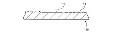
図1、図2は、本発明による一眼レフカメラ用ピント板10の一実施形態を示している。一眼レフカメラ用ピント板10は、周知のように、一眼レフカメラの撮像面と光学的に等価な位置に置かれるもので、撮影レンズによる被写体像が結像され、その被写体像が接眼レンズ(アイピース)によって観察者(撮影者)によって観察される。
1 and 2 show an embodiment of a
本実施形態の一眼レフカメラ用ピント板10は、全体がマット面11からなり、その中に、測距エリアや測光エリアを示す平面細線12を有している。マット面11は、ピント状態を確認するための拡散機能を有する程度の面粗さを持っている。パターンは種々知られており、その面粗さは例えばRaで0.5μm程度である。勿論、この面粗さの数値は一例であり、ピント状態を確認するという目的で使用可能なマット面であれば、これに限定されない。
The single-lens reflex
本実施形態の特徴とする平面細線12は、図2に示すように、一眼レフカメラ用ピント板10の板厚平面と平行な平面(鏡面)からなっている。マット面は、上述のように、ピント状態を確認するための拡散機能を有する面として定義されるのに対し、本実施形態の平面(鏡面)は、マット面より光透過率が高く、観察者にマット面より明るく視認することができる面と定義する。具体的には、その面粗さは、Raで0.01μm程度以下である。勿論、この面粗さの数値は一例であり、マット面の中でマット面より明るい線として視認されるという目的が達成できれば、これに限定されない。また、平面細線12の線幅は、50μmから500μm程度とするのがよい。これは、従来の断面V字型の細線の線幅が30μmから50μmであるのと比して広いが、従来の細線は黒く(暗く)認識されるのに対し、本実施形態の平面細線12は明るく認識されるため、幅を広くすることで視認を容易にしている。
As shown in FIG. 2, the thin
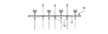
図3は、本実施形態の一眼レフカメラ用ピント板10の光線通過状況を模式的に示している。ピント板10に板面から直交する方向から入射した光線は、マット面11部分では拡散するのに対し、平面細線12部分では直進し(平面細線12での光透過率はマット面11での光透過率より高く)、観察者には、平面細線12部分がマット面11部分より明るく観察される。平面細線12は、一眼レフカメラ用ピント板10の板厚平面と厳密に平行にする必要はないが、あまり角度を付けると以上の作用が得られない。
FIG. 3 schematically shows a light beam passing situation of the focusing
本実施形態の一眼レフカメラ用ピント板10は、全体がマット面11のピント板10に対し、平面細線12を後加工して形成することが可能である。しかし、量産性を考慮すると、樹脂材料の成形品から構成するのが好ましい。
The focusing
図4は、フォトリソグラフィー技術と電鋳技術を用いた成形型の製造方法の一例を示している。最初に、基板20上にスピンコート法によってポジ型(又はネガ型)のフォトレジスト21を塗布し該フォトレジスト21の表面を可及的に平面とする(同図(A))。次に、マット面11に対応する拡散マスク11Xと平面細線12に対応する光透過線(又は光遮断線)12Xを有する光マスク22を用いて、フォトレジスト21上に紫外線を照射する(同図(B))。フォトレジスト21を現像すると、同図(C)のように、光透過線(又は光遮断線)12X部分は、フォトレジスト21の平面がそのまま残されて転写平面細線12Pが形成され、拡散マスク11X部分にはマット面に対応する凹凸を有する転写マット面11Pが形成される。このように形成した転写マット面11Pと転写平面細線12Pを有するフォトレジスト21上に、周知の手法により、Ni電鋳層23を形成していくと、該Ni電鋳層23によって一眼レフカメラ用ピント板10の成形型ができる(同図(D))。
FIG. 4 shows an example of a method for manufacturing a mold using a photolithography technique and an electroforming technique. First, a positive (or negative)
すなわち、このNi電鋳金型23には、転写平面細線12Pが転写された細線平面成形部12Mと、転写マット面11Pが転写されたマット面政経部11Mとが形成される。従ってこのNi電鋳型23によれば、本実施形態のピント板10を樹脂材料によって成形することができる。
That is, the Ni
以上の一眼レフカメラ用ピント板の成形型の製造方法によれば、従来のV溝加工のような後加工を施す必要がなく、容易に成形型を作成できる。 According to the method for manufacturing a mold for focusing on a single-lens reflex camera, it is not necessary to perform post-processing such as conventional V-groove processing, and a mold can be easily created.
10 一眼レフカメラ用ピント板
11 マット面
12 平面細線
20 基板
21 フォトレジスト
11P 転写マット面
12P 転写平面細線
22 光マスク
23 Ni電鋳層(成形型)
DESCRIPTION OF
Claims (6)
上記細線を、上記マット面より光透過率が高く、観察者にマット面より明るく視認される平面としたことを特徴とする一眼レフカメラ用ピント板。 In the focus plate for a single-lens reflex camera in which a thin line having a light transmittance different from that of the mat surface is drawn on the mat surface having a diffusion function for confirming the focus state,
A focusing plate for a single-lens reflex camera, characterized in that the thin line is a flat surface that has a light transmittance higher than that of the mat surface and is visible to an observer brighter than the mat surface.
Priority Applications (1)
| Application Number | Priority Date | Filing Date | Title |
|---|---|---|---|
| JP2008203702A JP5167021B2 (en) | 2008-08-07 | 2008-08-07 | Focus plate for single-lens reflex camera |
Applications Claiming Priority (1)
| Application Number | Priority Date | Filing Date | Title |
|---|---|---|---|
| JP2008203702A JP5167021B2 (en) | 2008-08-07 | 2008-08-07 | Focus plate for single-lens reflex camera |
Publications (2)
| Publication Number | Publication Date |
|---|---|
| JP2010039320A true JP2010039320A (en) | 2010-02-18 |
| JP5167021B2 JP5167021B2 (en) | 2013-03-21 |
Family
ID=42011924
Family Applications (1)
| Application Number | Title | Priority Date | Filing Date |
|---|---|---|---|
| JP2008203702A Active JP5167021B2 (en) | 2008-08-07 | 2008-08-07 | Focus plate for single-lens reflex camera |
Country Status (1)
| Country | Link |
|---|---|
| JP (1) | JP5167021B2 (en) |
Citations (6)
| Publication number | Priority date | Publication date | Assignee | Title |
|---|---|---|---|---|
| JPS55106438A (en) * | 1979-02-09 | 1980-08-15 | Ricoh Co Ltd | Focal plate in reflex camera |
| JPS56159624A (en) * | 1980-05-13 | 1981-12-09 | Minolta Camera Co Ltd | Display device for measurement region of autofocus detector of single-lens reflex camera |
| JPH01140135A (en) * | 1987-11-27 | 1989-06-01 | Takatoshi Ishii | Camera |
| JPH0320323U (en) * | 1989-07-07 | 1991-02-27 | ||
| JPH04114040U (en) * | 1991-03-22 | 1992-10-07 | 株式会社ニコン | Display observation device |
| JPH09218440A (en) * | 1996-02-15 | 1997-08-19 | Nikon Corp | Focal plane and photographic device using the same |
-
2008
- 2008-08-07 JP JP2008203702A patent/JP5167021B2/en active Active
Patent Citations (6)
| Publication number | Priority date | Publication date | Assignee | Title |
|---|---|---|---|---|
| JPS55106438A (en) * | 1979-02-09 | 1980-08-15 | Ricoh Co Ltd | Focal plate in reflex camera |
| JPS56159624A (en) * | 1980-05-13 | 1981-12-09 | Minolta Camera Co Ltd | Display device for measurement region of autofocus detector of single-lens reflex camera |
| JPH01140135A (en) * | 1987-11-27 | 1989-06-01 | Takatoshi Ishii | Camera |
| JPH0320323U (en) * | 1989-07-07 | 1991-02-27 | ||
| JPH04114040U (en) * | 1991-03-22 | 1992-10-07 | 株式会社ニコン | Display observation device |
| JPH09218440A (en) * | 1996-02-15 | 1997-08-19 | Nikon Corp | Focal plane and photographic device using the same |
Also Published As
| Publication number | Publication date |
|---|---|
| JP5167021B2 (en) | 2013-03-21 |
Similar Documents
| Publication | Publication Date | Title |
|---|---|---|
| US7336895B2 (en) | Diffuser panel and optical apparatus which uses this diffuser panel | |
| JP2572626B2 (en) | Method of forming reticle and microstructure array | |
| JP4845290B2 (en) | Micro lens array, optical equipment and optical viewfinder | |
| CN101533115A (en) | Diffractive optical element, optical system, and optical apparatus | |
| JP4981300B2 (en) | Focus plate and optical viewfinder having the same | |
| JP4316559B2 (en) | Light guide plate and manufacturing method thereof | |
| Nasse | Depth of field and bokeh | |
| JP2003080598A (en) | Forming method of microlens sheet, and microlens sheet obtained by this forming method | |
| JP2014508331A (en) | Optical unit | |
| JP5167021B2 (en) | Focus plate for single-lens reflex camera | |
| JP5686645B2 (en) | Focus plate and finder system having the same | |
| KR101182491B1 (en) | Optical film with partially coated structure array and manufacturing method thereof | |
| JP2015079128A (en) | Optical filter and imaging device | |
| JP2013246210A (en) | Method of fabricating microlens, microlens, counter substrate for liquid crystal device, and liquid crystal device | |
| JP3375352B2 (en) | Diffusion plate and method of manufacturing diffusion plate mold | |
| JP5668488B2 (en) | Photomask and method of manufacturing parallax crosstalk filter using the same | |
| JP2018151549A (en) | Diffuser panel and single lens reflex camera using the same at focusing screen | |
| JP4694560B2 (en) | Method of manufacturing molded sheet and lenticular lens sheet, and manufacturing apparatus thereof | |
| JP2008180970A (en) | Optical component with ruled line | |
| JP2007017686A (en) | Micro structural body and optical equipment device having the same | |
| JP2014238527A (en) | Nd filter for ultra-wide angle lens and fabrication method of the same | |
| JP4115165B2 (en) | Optical part molding method | |
| JPS5860642A (en) | Preparation of focusing glass | |
| JP2007304399A (en) | Rear projection screen and rear projection type display apparatus | |
| JP2007156055A (en) | Gray scale mask, manufacturing method of microlens, microlens, spatial optical modulating device, and projector |
Legal Events
| Date | Code | Title | Description |
|---|---|---|---|
| A621 | Written request for application examination |
Free format text: JAPANESE INTERMEDIATE CODE: A621 Effective date: 20110523 |
|
| A711 | Notification of change in applicant |
Free format text: JAPANESE INTERMEDIATE CODE: A711 Effective date: 20111208 |
|
| A711 | Notification of change in applicant |
Free format text: JAPANESE INTERMEDIATE CODE: A712 Effective date: 20111208 |
|
| A977 | Report on retrieval |
Free format text: JAPANESE INTERMEDIATE CODE: A971007 Effective date: 20121120 |
|
| TRDD | Decision of grant or rejection written | ||
| A01 | Written decision to grant a patent or to grant a registration (utility model) |
Free format text: JAPANESE INTERMEDIATE CODE: A01 Effective date: 20121204 |
|
| A61 | First payment of annual fees (during grant procedure) |
Free format text: JAPANESE INTERMEDIATE CODE: A61 Effective date: 20121221 |
|
| FPAY | Renewal fee payment (event date is renewal date of database) |
Free format text: PAYMENT UNTIL: 20151228 Year of fee payment: 3 |
|
| R150 | Certificate of patent or registration of utility model |
Free format text: JAPANESE INTERMEDIATE CODE: R150 Ref document number: 5167021 Country of ref document: JP Free format text: JAPANESE INTERMEDIATE CODE: R150 |
|
| S533 | Written request for registration of change of name |
Free format text: JAPANESE INTERMEDIATE CODE: R313533 |
|
| R350 | Written notification of registration of transfer |
Free format text: JAPANESE INTERMEDIATE CODE: R350 |
|
| R250 | Receipt of annual fees |
Free format text: JAPANESE INTERMEDIATE CODE: R250 |
|
| R250 | Receipt of annual fees |
Free format text: JAPANESE INTERMEDIATE CODE: R250 |
|
| R250 | Receipt of annual fees |
Free format text: JAPANESE INTERMEDIATE CODE: R250 |
|
| R250 | Receipt of annual fees |
Free format text: JAPANESE INTERMEDIATE CODE: R250 |
|
| R250 | Receipt of annual fees |
Free format text: JAPANESE INTERMEDIATE CODE: R250 |