JP2010028787A - Dual mode filter - Google Patents
Dual mode filter Download PDFInfo
- Publication number
- JP2010028787A JP2010028787A JP2008332782A JP2008332782A JP2010028787A JP 2010028787 A JP2010028787 A JP 2010028787A JP 2008332782 A JP2008332782 A JP 2008332782A JP 2008332782 A JP2008332782 A JP 2008332782A JP 2010028787 A JP2010028787 A JP 2010028787A
- Authority
- JP
- Japan
- Prior art keywords
- ring resonator
- line
- coupling point
- dual mode
- transmission line
- Prior art date
- Legal status (The legal status is an assumption and is not a legal conclusion. Google has not performed a legal analysis and makes no representation as to the accuracy of the status listed.)
- Granted
Links
Images


Classifications
-
- H—ELECTRICITY
- H01—ELECTRIC ELEMENTS
- H01P—WAVEGUIDES; RESONATORS, LINES, OR OTHER DEVICES OF THE WAVEGUIDE TYPE
- H01P1/00—Auxiliary devices
- H01P1/20—Frequency-selective devices, e.g. filters
- H01P1/201—Filters for transverse electromagnetic waves
- H01P1/203—Strip line filters
- H01P1/20327—Electromagnetic interstage coupling
- H01P1/20354—Non-comb or non-interdigital filters
- H01P1/20381—Special shape resonators
Abstract
Description
本発明は、リング状の伝送線路を含むデュアルモードフィルタに関する。 The present invention relates to a dual mode filter including a ring-shaped transmission line.
近年、携帯電話の普及、発展に伴い、高速かつ大容量の伝送技術が不可欠になってきている。高速かつ大容量の通信を実現するために、広い周波数帯域を確保する必要があり、無線通信で用いる周波数帯が高周波の方向へシフトしている。このような高周波帯域において、所望の周波数成分のみを選択的に通過させ、それ以外の周波数成分を急峻に遮断するフィルタ特性が、無線通信用のフィルタに求められる。また、高周波回路素子を用いた無線通信機器には、小型化及び軽量化も強く求められる。 In recent years, with the spread and development of mobile phones, high-speed and large-capacity transmission technology has become indispensable. In order to realize high-speed and large-capacity communication, it is necessary to secure a wide frequency band, and the frequency band used for wireless communication is shifted toward higher frequencies. In such a high-frequency band, a filter characteristic for selectively passing only a desired frequency component and steeply blocking other frequency components is required for a filter for wireless communication. Further, miniaturization and weight reduction are strongly demanded for radio communication equipment using high-frequency circuit elements.
高周波数帯域で用いられるフィルタとして、リング状の伝送線路からなるリング共振器を含むフィルタが知られている。リング共振器の共振周波数は、その電気線路長により特定される。共振波長またはその整数倍が、リング共振器の電気線路長と等しくなる。リング共振器のスペース効率を高めるために、1つのリング共振器を2つの共振モード(デュアルモード)で共振させて、より急峻なフィルタ特性を得る方法が提案されている。 As a filter used in a high frequency band, a filter including a ring resonator composed of a ring-shaped transmission line is known. The resonance frequency of the ring resonator is specified by its electrical line length. The resonance wavelength or an integral multiple of the resonance wavelength is equal to the electrical line length of the ring resonator. In order to increase the space efficiency of the ring resonator, a method has been proposed in which one ring resonator is resonated in two resonance modes (dual mode) to obtain steeper filter characteristics.
リング共振器上で1/4波長に相当する線路長だけ離れた2点において、入力線路及び出力線路が、リング共振器に結合する。この2つの結合点の間にスタブを設けることにより、デュアルモードの発振が生ずる(特許文献1)。リング共振器の外側に、その外周の一部に沿って分布結合線路を配置することによっても、デュアルモードの発振が生ずる(特許文献2)。この分布結合線路は、入力線路及び出力線路に結合する2つの結合点を両端とする2本の伝送線路のうち長い方の伝送線路のほぼ中央において、リング共振器に並走するように配置される。 The input line and the output line are coupled to the ring resonator at two points separated by a line length corresponding to a quarter wavelength on the ring resonator. By providing a stub between the two coupling points, dual mode oscillation occurs (Patent Document 1). Dual mode oscillation also occurs by disposing a distributed coupling line along a part of the outer periphery of the ring resonator (Patent Document 2). This distributed coupled line is arranged so as to run parallel to the ring resonator at the approximate center of the longer transmission line of the two transmission lines having two coupling points coupled to the input line and the output line as both ends. The
リング共振器にスタブを設けると、スタブの近傍に電流が集中する。このため、耐電力特性が低下してしまう。リング共振器の外側に分布結合線路を配置する構成では、電流の集中が生じにくい。 When a stub is provided in the ring resonator, current is concentrated in the vicinity of the stub. For this reason, a power durability characteristic will fall. In the configuration in which the distributed coupling line is disposed outside the ring resonator, current concentration is unlikely to occur.
本発明においては、電流の集中が生じにくい新たな構成を有するデュアルモードフィルタが提供される。 In the present invention, a dual mode filter having a new configuration in which current concentration hardly occurs is provided.
電流の集中が生じにくいデュアルモードフィルタは、
伝送線路をリング状にしたリング共振器と、
前記リング共振器上の第1の結合点において、該リング共振器に電磁気的に結合する入力フィーダと、
前記リング共振器上の、前記第1の結合点とは異なる第2の結合点において、該リング共振器に電磁気的に結合する出力フィーダと、
前記リング共振器の内側に配置され、該リング共振器上の第3の結合点において、一方の端部が該リング共振器に容量結合し、該第3の結合点から該リング共振器の線路長の1/2の長さだけ離れた第4の結合点において、他方の端部が該リング共振器に容量結合するデュアルモード発生線路と
を有する。
Dual mode filters that are less likely to concentrate current
A ring resonator having a ring-shaped transmission line;
An input feeder electromagnetically coupled to the ring resonator at a first coupling point on the ring resonator;
An output feeder that electromagnetically couples to the ring resonator at a second coupling point on the ring resonator that is different from the first coupling point;
The ring resonator is disposed inside the ring resonator, and at a third coupling point on the ring resonator, one end is capacitively coupled to the ring resonator, and the line of the ring resonator is coupled from the third coupling point. At a fourth coupling point separated by a length of ½, the other end has a dual mode generation line that is capacitively coupled to the ring resonator.
リング共振器にスタブが設けられていないため、電流の集中を抑制することができる。 Since the ring resonator is not provided with a stub, current concentration can be suppressed.
以下、地面を参照して実施例について説明する。 Hereinafter, examples will be described with reference to the ground.
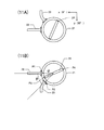
図1Aに、第1の実施例によるデュアルモードフィルタの断面図を示し、図1Bに、図1Aの一点鎖線1B−1Bにおける平断面図を示す。図1Bの一点鎖線1A−1Aにおける断面図が図1Aに相当する。
FIG. 1A shows a cross-sectional view of the dual mode filter according to the first embodiment, and FIG. 1B shows a cross-sectional plan view taken along one-
主表面上にリング共振器21等が形成され、裏面にグランド膜27が形成された誘電体基板20が、パッケージ15の本体15Aの底面上に配置されている。グランド膜27がパッケージ本体15Aの底面に接触する。
A
パッケージ本体15Aは、上方が開口した直方体状の容器であり、開口部は、天板15Bで塞がれている。パッケージ本体15Aと天板15Bとにより、内部に閉じた空間を画定するパッケージ15が構成される。パッケージ15は、例えば、熱伝導性及び導電性に優れる無酸素銅で形成されている。なお、無酸素銅の他に、純アルミニウム、アルミニウム合金、銅合金等で形成してもよい。さらに、熱収縮率が誘電体基板20のそれに近いコバール、インバー、42アロイ等で形成してもよい。また、パッケージ15には、表面酸化による電気的な特性の劣化を防止するために、厚さ2μm程度の金めっきが施されている。
The
誘電体基板20は、主表面に(100)結晶面が現れている酸化マグネシウム(MgO)で形成され、その厚さは0.5mmである。誘電体基板20の材料として、LaAlO3、サファイア等の高誘電率、低損失の誘電体材料を用いてもよい。
The
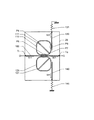
図1Bに示すように、誘電体基板20の主表面上に、リング共振器21、入力フィーダ22、出力フィーダ23、及びデュアルモード発生線路24が形成されている。リング共振器21、入力フィーダ22、出力フィーダ23、デュアルモード発生線路24、及びグランド膜27は、マイクロストリップライン構造を有する。誘電体基板20の主表面に、xy直交座標系を定義し、x軸の正の向きの方位角を0°とし、y軸の正の向きの方位角を90°とする。
As shown in FIG. 1B, a
リング共振器21は、円周状の伝送線路で構成される。誘電体基板20の上に5GHz帯のバンドパスフィルタを作製する場合、リング共振器21を構成する伝送線路の幅を、0.5mmとし、伝送線路の中心線が描く円周の半径(中心半径)を3.65mmとする。
The
入力フィーダ22は、リング共振器21の中心から方位角0°の方向に伸ばした仮想直線に沿って、リング共振器21の外側に配置される。リング共振器21上の方位角0°の点(第1の結合点)P1において、入力フィーダ22とリング共振器21とが電磁気的に結合する。出力フィーダ23は、リング共振器21の中心から方位角90°の方向に伸ばした仮想直線に沿って、リング共振器21の外側に配置される。リング共振器21上の方位角90°の点(第2の結合点)P2において、出力フィーダ23とリング共振器21とが電磁気的に結合する。すなわち、第1の結合点P1から第2の結合点P2までの線路長は、リング共振器21の線路長の1/4になる。入力フィーダ22及び出力フィーダ23の各々の線幅は、0.5mmであり、リング共振器21と結合する端部において拡幅されている。
The
デュアルモード発生線路24は、リング共振器21の内側に配置される。デュアルモード発生線路24の両端が、それぞれリング共振器21上の第3の結合点P3及び第4の結合点P4において、リング共振器21に容量結合する。第3の結合点P3は、リング共振器21の中心から方位角45°の方向に伸びる仮想直線と、リング共振器21との交差箇所に位置する。第4の結合点P4は、リング共振器21の中心から方位角235°の方向に伸びる仮想直線と、リング共振器21との交差箇所に位置する。本明細書において、リング共振器21上の任意の点の位置を、リング共振器21からその点に向かう仮想直線の方位角で表すこととする。
The dual
第3の結合点P3は、第1の結合点P1と第2の結合点P2とを両端とする伝送線路のうち短い方の伝送線路の中点に位置し、第4の結合点P4は、長い方の伝送線路の中点に位置する。すなわち、第3の結合点P3から第4の結合点P4までの線路長は、リング共振器21の線路長の1/2である。
The third coupling point P3 is located at the midpoint of the shorter transmission line of the transmission lines having both ends of the first coupling point P1 and the second coupling point P2, and the fourth coupling point P4 is Located at the midpoint of the longer transmission line. That is, the line length from the third coupling point P3 to the fourth coupling point P4 is ½ of the line length of the
デュアルモード発生線路24は直線状の伝送線路であり、その線路幅は、例えば0.5〜1.2mmである。デュアルモード発生線路24の端部とリング共振器21との間の間隙は、例えば75〜125μmである。デュアルモード発生線路24の両端の縁は、リング共振器21の内周側の縁に沿う円弧状の形状を有する。なお、入力フィーダ22のように、デュアルモード発生線路24の端部を拡幅させた形状としてもよい。
The dual
リング共振器21内で共振する高周波信号の波長λrと、リング共振器21の中心半径rとの関係は、
2πr=n×λr (nは自然数) ・・・(1)
となる。n=1のときの波長λrを「基本共振波長」、基本共振波長を持つ高周波信号の周波数を「基本共振周波数」という。中心半径rが3.65mmのとき、基本共振波長は22.9mmになる。なお、実際の共振波長は、マイクロストリップラインの実効誘電率と、電気的に測定された共振周波数とから求めることができる。
The relationship between the wavelength λr of the high frequency signal resonating in the
2πr = n × λr (n is a natural number) (1)
It becomes. The wavelength λr when n = 1 is referred to as “basic resonance wavelength”, and the frequency of a high-frequency signal having the fundamental resonance wavelength is referred to as “basic resonance frequency”. When the center radius r is 3.65 mm, the fundamental resonance wavelength is 22.9 mm. The actual resonance wavelength can be obtained from the effective dielectric constant of the microstrip line and the electrically measured resonance frequency.
リング共振器21、入力フィーダ22、出力フィーダ23、デュアルモード発生線路24、及びグランド膜27は、YBa2Cu3O7−x(以下、「YBCO」という。)で形成されており、その厚さは100〜500nmである。なお、YBCOに代えて、液体窒素温度で超伝導状態を示す他の酸化物超伝導材料を用いてもよい。酸化物超伝導材料の例として、R−Ba−Cu−O系(RはNb、Ym、Sm、またはHo)材料、Bi−Sr−Ca−Cu−O系材料、Pb−Bi−Sr−Ca−Cu−O系材料、CuBapCaqCurOx系材料(1.5<p<2.5、2.5<q<3.5、3.5<r<4.5)等が挙げられる。
The
YBCO膜は、例えばパルスレーザ蒸着法により形成することができる。誘電体基板20の主表面上の各YBCOパターンは、通常のフォトリソグラフィ技術及びウェットエッチングにより形成することができる。Cr膜、Pd膜、及びAu膜が積層された電極は、蒸着及びリフトオフ法を用いて形成することができる。
The YBCO film can be formed by, for example, a pulse laser deposition method. Each YBCO pattern on the main surface of the
入力フィーダ22及び出力フィーダ23の各々の、リング共振器21から遠い方の端部近傍の表面上に、Cr膜、Pd膜、及びAu膜がこの順番に積層された電極が形成されている。
On the surface of each of the
パッケージ本体15Aの側壁に、同軸の入力コネクタ35及び同軸の出力コネクタ36が取り付けられている。入力コネクタ35の中心導体が、直径25μmのAu線により入力フィーダ22の端部の電極に接続され、出力コネクタ36の中心導体が、直径25μmのAu線により出力フィーダ23の端部の電極に接続されている。Au線の代わりに、AuリボンやAl線を用いてもよい。
A
図2に、リング共振器21、入力フィーダ22、出力フィーダ23、及びデュアルモード発生線路24の平面図を示す。第3の結合点P3は、方位角φが45°の位置に配置される。デュアルモード発生線路24の線路幅をW、デュアルモード発生線路24の端部とリング共振器21との間の間隙をGとする。
FIG. 2 shows a plan view of the
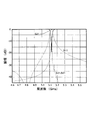
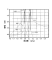
図3Aに、デュアルモード発生線路24の線路幅Wを0.50mm、0.85mm、及び1.20mmとしたときのフィルタ特性のシミュレーション結果を示す。横軸は、周波数を単位「GHz」で表し、縦軸はSパラメータの大きさを単位「dB」で表す。なお、間隙Gは0.10mmとした。
FIG. 3A shows the simulation results of the filter characteristics when the line width W of the dual
シミュレーション結果から、デュアルモードの共振が発生していることがわかる。通過帯域の両側に、それぞれ減衰極が現れている。 From the simulation results, it can be seen that dual mode resonance occurs. Attenuation poles appear on both sides of the passband.
図3Bに、図3Aに示したシミュレーション結果から算出された通過帯域幅と線路幅Wとの関係を示す。横軸は、線路幅Wを単位「mm」で表し、縦軸は、通過帯域幅を単位「MHz」で表す。デュアルモード発生線路24の線路幅が太くなるに従って、通過帯域幅が広くなることがわかる。
FIG. 3B shows the relationship between the pass bandwidth calculated from the simulation result shown in FIG. 3A and the line width W. The horizontal axis represents the line width W in the unit “mm”, and the vertical axis represents the passband width in the unit “MHz”. It can be seen that the passband width increases as the line width of the dual
図4Aに、間隙Gを75μm、100μm、及び125μmとしたときのフィルタ特性のシミュレーション結果を示す。横軸は、周波数を単位「GHz」で表し、縦軸はSパラメータの大きさを単位「dB」で表す。なお、線路幅Wは0.85mmとした。 FIG. 4A shows simulation results of filter characteristics when the gap G is 75 μm, 100 μm, and 125 μm. The horizontal axis represents the frequency in the unit “GHz”, and the vertical axis represents the size of the S parameter in the unit “dB”. The line width W was 0.85 mm.
図4Bに、図4Aに示したシミュレーション結果から算出された通過帯域幅と間隙Gとの関係を示す。横軸は、間隙Gを単位「μm」で表し、縦軸は、通過帯域幅を単位「MHz」で表す。間隙Gが狭くなるに従って、すなわちデュアルモード発生線路24とリング共振器21との結合容量が大きくなるに従って、通過帯域幅が広くなることがわかる。
FIG. 4B shows the relationship between the pass bandwidth calculated from the simulation result shown in FIG. 4A and the gap G. The horizontal axis represents the gap G in the unit “μm”, and the vertical axis represents the passband width in the unit “MHz”. It can be seen that the passband width increases as the gap G decreases, that is, as the coupling capacitance between the dual
図3A〜図4Bに示したシミュレーション結果からわかるように、デュアルモード発生線路24の線路幅W、及びデュアルモード発生線路24の端部とリング共振器21との間の間隙Gの少なくとも一方を変えることにより、通過帯域幅を制御することが可能である。
As can be seen from the simulation results shown in FIGS. 3A to 4B, at least one of the line width W of the dual
第1の実施例によるデュアルモードフィルタのリング共振器21とデュアルモード発生線路24とからなる平面パターンは、第3の結合点P3と第4の結合点P4とを通過する第1の直線に関して線対称である。さらに、第1の直線に直交し、リング共振器21の中心を通過する第2の直線に関しても線対称である。
The plane pattern composed of the
上記第1の実施例では、第3の結合点P3が、第1の結合点P1と第2の結合点P2とを両端とする伝送線路の中点に位置していた。次に、第3の結合点P3が、中点からややずれている場合について、フィルタ特性のシミュレーションを行った。 In the first embodiment, the third coupling point P3 is located at the midpoint of the transmission line having the first coupling point P1 and the second coupling point P2 as both ends. Next, the filter characteristics were simulated for the case where the third coupling point P3 is slightly shifted from the middle point.
図5に、そのシミュレーション結果を示す。第3の結合点P3の位置を示す方位角φが45°、45°±1°、及び45°±5°の場合について、透過特性及び反射特性を算出した。方位角φが45°から1°ずれた場合、S11が小さくなっているが、これは通過帯域幅が狭くなっているためである。 FIG. 5 shows the simulation result. Transmission characteristics and reflection characteristics were calculated for azimuth angles φ indicating the position of the third coupling point P3 of 45 °, 45 ° ± 1 °, and 45 ° ± 5 °. If the azimuth angle φ is shifted 1 ° from 45 °, although S 11 is reduced, this is because the pass band width is narrow.
第3の結合点P3の位置を示す方位角φが45°から±5°ずれると、通過帯域幅が狭くなっているにも係わらずS11が大きくなっている。すなわち反射特性が悪化している。方位角φの、45°からのずれが5°を超えると、反射特性がさらに悪化する。方位角φの、45°からのずれが5°以下であれば、実用可能な高周波フィルタが得られる。 When the azimuth angle φ indicating the position of the third coupling point P3 is shifted ± 5 ° from 45 °, S 11 is increased despite the pass band width is narrowed. That is, the reflection characteristics are deteriorated. When the deviation of the azimuth angle φ from 45 ° exceeds 5 °, the reflection characteristics are further deteriorated. If the deviation of the azimuth angle φ from 45 ° is 5 ° or less, a practical high-frequency filter can be obtained.
方位角φの5°のずれは、リング共振器21の線路長の約1.4%に相当する。従って、第1の結合点P1と第2の結合点P2とを両端とする短い方の伝送線路の中点から、第3の結合点P3までの線路長を、リング共振器21の線路長の1.4%以下とすることが好ましい。
A shift of 5 ° in the azimuth angle φ corresponds to about 1.4% of the line length of the
上記第1の実施例では、リング共振器21、入力フィーダ22、出力フィーダ23、デュアルモード発生線路24、及びグランド膜27に、酸化物超伝導材料を用いたが、常伝導材料、例えば銅(Cu)を用いてもよい。
In the first embodiment, an oxide superconductive material is used for the
図6に、酸化物超伝導材料に代えて銅を用いた場合の、フィルタ特性のシミュレーション結果を示す。第3の結合点P3の位置を示す方位角φを45°とし、デュアルモード発生線路24の線路幅Wを0.85mmとし、間隙Gを0.10mmとした。電気抵抗に起因する損失のため、超伝導材料を用いた場合に比べて透過特性及び反射特性が悪くなっているが、実用可能なフィルタ特性が得られている。
FIG. 6 shows a simulation result of filter characteristics when copper is used instead of the oxide superconducting material. The azimuth angle φ indicating the position of the third coupling point P3 was 45 °, the line width W of the dual
次に、図7A及び図7Bを参照して、第2の実施例によるデュアルモードフィルタについて説明する。 Next, a dual mode filter according to the second embodiment will be described with reference to FIGS. 7A and 7B.
図7Aに、第2の実施例によるデュアルモードフィルタの主要部の平面図を示す。第1の実施例では、第3の結合点P3の位置を示す方位角φが45°であったが、第2の実施例では、方位角φが135°である。第4の結合点P4の位置を示す方位角は315°になる。その他の構成は、第1の実施例によるデュアルモードフィルタと同一である。 FIG. 7A is a plan view of the main part of the dual mode filter according to the second embodiment. In the first embodiment, the azimuth angle φ indicating the position of the third coupling point P3 is 45 °. In the second embodiment, the azimuth angle φ is 135 °. The azimuth angle indicating the position of the fourth coupling point P4 is 315 °. Other configurations are the same as those of the dual mode filter according to the first embodiment.
第2の実施例では、第1の結合点P1と第2の結合点P2とを両端とする短い方の伝送線路の中点から、第3の結合点P3までの線路長が、リング共振器21の線路長の1/4になる。 In the second embodiment, the line length from the middle point of the shorter transmission line having both the first coupling point P1 and the second coupling point P2 to the third coupling point P3 is the ring resonator. It becomes 1/4 of the line length of 21.
図7Bに、第2の実施例によるデュアルモードフィルタのフィルタ特性のシミュレーション結果を示す。デュアルモード発生線路24の線路幅Wを0.85mmとし、間隙Gを0.10mmとした。第2の実施例においても、デュアルモードの共振が生じていることがわかる。ただし、第1の実施例の場合とは異なり、通過帯域の両側に減衰極は現れていない。
FIG. 7B shows a simulation result of the filter characteristics of the dual mode filter according to the second embodiment. The line width W of the dual
上記第2の実施例では、第1の結合点P1と第2の結合点P2とを両端とする短い方の伝送線路の中点からの線路長が、リング共振器21の線路長の1/4となる位置に、第3の結合点P3を配置した。第1の実施例の場合と同様に、この位置からの線路長が、リング共振器21の線路長の1.4%以下となる位置に第3の結合点P3を配置してもよい。
In the second embodiment, the line length from the midpoint of the shorter transmission line having the first coupling point P1 and the second coupling point P2 as both ends is 1 / of the line length of the
図8に、第3の実施例によるデュアルモードフィルタの主要部の断面図を示す。第1及び第2の実施例では、リング共振器21等の片側にのみグランド膜27を配置したマイクロストリップラインが採用された。第3の実施例では、リング共振器21等の両側にグランド膜を配置したストリップライン構造が採用される。
FIG. 8 shows a cross-sectional view of the main part of the dual mode filter according to the third embodiment. In the first and second embodiments, a microstrip line in which the
誘電体基板20、その主表面上のリング共振器21等、その裏面上のグランド膜27の構成は、第1の実施例の構成と同一である。誘電体基板20の主表面上に、リング共振器21等を覆うように、誘電体膜60が配置されている。この誘電体膜60の表面上に、上側のグランド膜61が形成されている。
The configuration of the
このように、ストリップライン構造としても、第1の実施例のマイクロストリップライン構造の場合と同様の効果が得られる。 As described above, the strip line structure can provide the same effect as that of the microstrip line structure of the first embodiment.
図9Aに、第4の実施例によるデュアルモードフィルタの断面図を示す。図9Bに、図9Aの一点鎖線9B−9Bにおける平断面図を示す。図9Bの一点鎖線9A−9Aにおける断面図が、図9Aに相当する。以下、図1A及び図1Bに示した第1の実施例によるデュアルモードフィルタとの相違点に着目して説明し、構成が同一の部分については説明を省略する。
FIG. 9A is a sectional view of a dual mode filter according to the fourth embodiment. FIG. 9B is a plan sectional view taken along one-
誘電体基板20の上方に、第1の誘電体部材71及び第2の誘電体部材72が配置されている。第1の誘電体部材71は、第3の結合点P3の近傍に配置され、第2の誘電体部材72は、第4の結合点P4の近傍に配置されている。ここで、「近傍」とは、リング共振器21とデュアルモード発生線路24との結合部に発生する電磁界の影響の及ぶ範囲と定義することができる。第1の誘電体部材71及び第2の誘電体部材72には、MgO等を用いることができる。
A
第1の誘電体部材71は、第1の支持部材73によりパッケージ15に支持されている。第1の支持部材73は、第1の誘電体部材71を昇降させることができる。すなわち、第1の誘電体部材71と誘電体基板20との間隔を変化させることができる。第1の誘電体部材71を最も下降させた状態では、第1の誘電体部材71が、リング共振器21及びデュアルモード発生線路24に接触する。
The
第1の支持部材73には、例えばパッケージ15の天板15Bに形成された貫通孔に螺号するネジを用いることができる。ネジを回転させることにより、第1の誘電体部材71を昇降させることができる。なお、第1の支持部材73に、外部からの駆動信号によって対象物を並進移動させるリニアアクチュエータを用いてもよい。
As the
第2の誘電体部材72は、第1の誘電体部材71と同様に、第2の支持部材74によりパッケージ15に昇降可能に支持されている。
Similar to the
第1の誘電体部材71及び第2の誘電体部材72を昇降させると、リング共振器21とデュアルモード発生線路24との結合容量が変化する。これは、デュアルモード発生線路24の端部とリング共振器21との間の間隙Gが変化したことと等価である。このため、第1の誘電体部材71及び第2の誘電体部材72の少なくとも一方を昇降させることにより、フィルタの通過帯域幅を変化させることができる。
When the
図10Aに、第5の実施例によるデュアルモードフィルタの主要部の平面図を示す。第1の実施例では、出力フィーダ23とリング共振器21とが結合する第2の結合点P2が、方位角90°の位置に配置されていた。第5の実施例では、第2の結合点P2の位置を示す方位角θが45°である。第3の結合点P3の位置を示す方位角φが112.5°、第4の結合点P4の位置を示す方位角が292.5°である。その他の構成は、第1の実施例によるデュアルモードフィルタの構成と同一である。
FIG. 10A is a plan view of the main part of the dual mode filter according to the fifth embodiment. In the first embodiment, the second coupling point P2 where the
第5の実施例では、第1の結合点P1から第2の結合点P2までの線路長が、リング共振器21の線路長の1/8である。また、第2の実施例の場合と同様に、第1の結合点P1と第2の結合点P2とを両端とする短い方の伝送線路の中点から第3の結合点P3までの線路長が、リング共振器21の線路長の1/4である。
In the fifth embodiment, the line length from the first
第1の結合点P1から第2の結合点P2までの線路長が、リング共振器21の線路長の1/8であるため、基本共振周波数の高周波信号は、入力フィーダ22から出力フィーダ23まで殆ど伝達されず、基本共振周波数の2倍の周波数の高周波信号が、出力フィーダ23まで伝達される。
Since the line length from the first coupling point P1 to the second coupling point P2 is 1/8 of the line length of the
図10Bに、第5の実施例によるデュアルモードフィルタのフィルタ特性を示す。デュアルモード発生線路24の線路幅Wは0.5mm、間隙Gは0.1mmとした。第1の実施例によるフィルタの通過帯域は5GHz近傍であったが、第5の実施例によるフィルタの通過帯域は10GHz近傍である。第5の実施例でも、デュアルモードの共振が発生しており、通過帯域の両側に減衰極が現れている。
FIG. 10B shows the filter characteristics of the dual mode filter according to the fifth embodiment. The dual
図11Aに第5の実施例の変形例によるデュアルモードフィルタの主要部の平面図を示す。図11Aに示したフィルタのリング共振器21、入力フィーダ24、出力フィーダ23、及びデュアルモード発生線路24の平面パターンは、図10Aに示した第5の実施例によるこれらの平面パターンと鏡像の関係にある。
FIG. 11A is a plan view of the main part of a dual mode filter according to a modification of the fifth embodiment. The plane patterns of the
図1B及び図2に示した第1の実施例、図7Aに示した第2の実施例についても、リング共振器21、入力フィーダ24、出力フィーダ23、及びデュアルモード発生線路24の平面パターンに対して鏡像の関係を持つ平面パターンのデュアルモードフィルタを作製することができる。
In the first embodiment shown in FIGS. 1B and 2 and the second embodiment shown in FIG. 7A as well, the plane pattern of the
図11Bに、第6の実施例によるデュアルモードフィルタの主要部の平面図を示す。図11Bに示した例では、第3の結合点P3の位置を示す方位角φが22.5°であり、第4の結合点P4の位置を示す方位角が202.5°である。すなわち、第3の結合点P3は、第1の結合点P1と第2の結合点P2とを両端とする短い方の伝送線路の中点に位置する。 FIG. 11B is a plan view of the main part of the dual mode filter according to the sixth embodiment. In the example shown in FIG. 11B, the azimuth angle φ indicating the position of the third coupling point P3 is 22.5 °, and the azimuth angle indicating the position of the fourth coupling point P4 is 202.5 °. That is, the third coupling point P3 is located at the midpoint of the shorter transmission line having both the first coupling point P1 and the second coupling point P2 as both ends.
図12Aに、第7の実施例によるデュアルモードフィルタの主要部の平面図を示す。第7の実施例では、第2の結合点P2の位置を示す方位角θが135°である。すなわち、第1の結合点P1から第2の結合点P2までの線路長が、リング共振器21の線路長の3/8になる。第3の結合点P3の位置を示す方位角φは、67.5°である。すなわち、第3の結合点P3は、第1の結合点P1と第2の結合点P2とを両端とする短い方の伝送線路の中点に位置する。
FIG. 12A is a plan view of the main part of the dual mode filter according to the seventh embodiment. In the seventh embodiment, the azimuth angle θ indicating the position of the second coupling point P2 is 135 °. That is, the line length from the first coupling point P1 to the second coupling point P2 is 3/8 of the line length of the
図12Bに、図12Aに示したデュアルモードフィルタの鏡像パターンを持つフィルタの平面図を示す。 FIG. 12B shows a plan view of a filter having a mirror image pattern of the dual mode filter shown in FIG. 12A.
図12Cに、第8の実施例によるデュアルモードフィルタの主要部の平面図を示す。第8の実施例では、第2の結合点P2の位置を示す方位角が135°であり、図12Aに示した実施例と同一である。第3の結合点P3及び第4の結合点P4の位置を示す方位角は、それぞれ157.5°及び337.5°である。すなわち、図7Aに示した第2の実施例と同様に、第1の結合点P1と第2の結合点P2とを両端とする短い方の伝送線路の中点から、第3の結合点P3までの線路長が、リング共振器21の線路長の1/4である。
FIG. 12C is a plan view of the main part of the dual mode filter according to the eighth embodiment. In the eighth embodiment, the azimuth angle indicating the position of the second coupling point P2 is 135 °, which is the same as the embodiment shown in FIG. 12A. The azimuth angles indicating the positions of the third coupling point P3 and the fourth coupling point P4 are 157.5 ° and 337.5 °, respectively. That is, similar to the second embodiment shown in FIG. 7A, the third coupling point P3 is determined from the middle point of the shorter transmission line having both the first coupling point P1 and the second coupling point P2 as both ends. The line length up to ¼ is the line length of the
第8の実施例についても、鏡像パターンを持つデュアルモードフィルタを作製することができる。 Also in the eighth embodiment, a dual mode filter having a mirror image pattern can be manufactured.
第6〜第8の実施例によるデュアルモードフィルタは、第5の実施例と同様に、10GHz帯のフィルタとして動作する。 The dual mode filter according to the sixth to eighth embodiments operates as a 10 GHz band filter as in the fifth embodiment.
図13に、第9の実施例によるデュアルモードフィルタの誘電体基板上の導電パターンを示す。 FIG. 13 shows a conductive pattern on a dielectric substrate of a dual mode filter according to the ninth embodiment.
誘電体基板20の上に、直線状の主伝送線路100が形成されている。主伝送線路100の一端(図13の左端)が入力端Tiとなり、他端(図13の右端)が出力端Toとなる。主伝送線路100の両脇に、それぞれ第1のリング共振器110及び第2のリング共振器120が形成されている。図1Bに示した第1の実施例のリング共振器21は、円周に沿う平面形状を有していたが、第9の実施例の第1のリング共振器110及び第2のリング共振器120の平面形状は、角が丸くなった正方形の外周に沿う平面形状を有する。すなわち、第1のリング共振器110及び第2のリング共振器120の各々は、正方形の4本の辺に沿う4本の直線部分と、隣り合う直線部分同士を接続する中心角90°の円弧に沿う部分とで構成される。
A linear
第1のリング共振器110の1つの直線部分が、主伝送線路100の脇に、主伝送線路100と平行になるように配置され、結合箇所P5において主伝送線路100と電磁気的に結合する。第1のリング共振器110の平面形状を円周状にした場合と比べて、主伝送線路100と第1のリング共振器110との結合が強くなる。
One linear portion of the
第1のリング共振器110の他の直線部分に沿うように、第1のリング共振器110の外側に、直線状の第1の副伝送線路130が配置されている。第1の副伝送線路130は、結合箇所P6において、第1のリング共振器110に結合する。第1の副伝送線路130が結合する直線部分は、主伝送線路100が結合する直線部分と隣り合う。すなわち、第1のリング共振器110のうち、主伝送線路100との結合箇所P5から、第1の副伝送線路130との結合箇所P6までの線路長は、第1のリング共振器110の線路長の1/4である。第1の副伝送線路130の延在する方向は、主伝送線路100の延在する方向と直交する。このため、第1の副伝送線路130が、直接、主伝送線路100に結合することはない。
A straight first
第1のリング共振器110の内側に、第1のデュアルモード発生線路111が形成されている。第1のデュアルモード発生線路111は、その両端において第1のリング共振器110に容量結合する。一方の端部が結合する箇所P7から、他方の端部が結合する箇所P8までの線路長は、第1の実施例の場合と同様に、第1のリング共振器110の線路長の1/2である。
A first dual
図13に示した例では、第1のデュアルモード発生線路111の一方の端部は、主伝送線路100に結合する直線部分と、第1の副伝送線路130に結合する直線部分とを接続している円弧部分の中点P7において、第1のリング共振器110に結合している。他方の端部は、対角に位置する円弧部分の中点P8において、第1のリング共振器110に結合している。すなわち、第1のデュアルモード発生線路111の両端は、それぞれ第1のリング共振器110のうち、主伝送線路100との結合箇所P5から、第1の副伝送線路との結合箇所P6に至る2つの伝送線路部分の中間地点P7、P8において、第1のリング共振器110に結合している。
In the example shown in FIG. 13, one end of the first dual
第2のリング共振器120、第2のデュアルモード発生線路121、第2の副伝送線路140は、主伝送線路100に関して、第1のリング共振器110、第1のデュアルモード発生線路111、第1の副伝送線路130と線対称の平面形状を有する。
The
これらの伝送線路は、例えば、厚さ500nmのYBCO膜で形成される。主伝送線路100、第1及び第2の副伝送線路130、140、第1及び第2のリング共振器110、120の線路幅は、0.5mmである。第1及び第2のデュアルモード発生線路111、121の線路幅は0.85mmである。第1及び第2のリング共振器110、120の線路長は、中心半径3.65mmの円周状のリング共振器の線路長と同一である。リング共振器の直線部分と、それに結合する伝送線路との間隔は、100μmである。
These transmission lines are formed of a YBCO film having a thickness of 500 nm, for example. The line width of the
この誘電体基板20が、図1Bに示した第1の実施例のパッケージ15と同様のパッケージに収容される。入力端Ti、出力端To、第1の副伝送線路130の出力端、及び第2の副伝送線路140の出力端が、パッケージに取り付けられたコネクタを介して、パッケージ外に引き出される。
This
第1の副伝送線路130の出力端は、パッケージ外に配置される第1の終端抵抗131を介して接地される。第1の終端抵抗131のインピーダンスは、第1の副伝送線路130の特性インピーダンスにマッチングする。同様に、第2の副伝送線路140の出力端も、第2の終端抵抗141を介して接地される。
The output terminal of the first
入力端Tiから入力された高周波信号のうち、第1及び第2のリング共振器110、120に共振する周波数成分が、第1及び第2のリング共振器110、120を経由して、第1及び第2の副伝送線路130、140まで伝搬する。第1及び第2の副伝送線路130、140まで伝搬した高周波信号の電力は、終端抵抗131、141で消費される。
Of the high-frequency signal input from the input terminal Ti, the frequency component that resonates with the first and
入力端Tiから入力された高周波信号のうち、第1及び第2のリング共振器110、120と共振しない周波数成分は、主伝送線路100をそのまま伝搬し、出力端Toまで達する。
Of the high-frequency signal input from the input terminal Ti, the frequency component that does not resonate with the first and
図14に、各伝送線路を伝搬する信号の振幅のスペクトルのシミュレーション結果を示す。図14に示した実線S21は、出力端Toに出力される信号の振幅を示し、点線S11は、入力端Tiに戻ってくる反射波の振幅を示し、破線S31及びS41は、第1及び第2の副伝送線路130、140の出力端に出力される信号の振幅を示す。第1及び第2のリング共振器110、120の共振周波数は約5.13GHzである。
FIG. 14 shows a simulation result of the spectrum of the amplitude of the signal propagating through each transmission line. The solid line S21 shown in FIG. 14 indicates the amplitude of the signal output to the output terminal To, the dotted line S11 indicates the amplitude of the reflected wave returning to the input terminal Ti, and the broken lines S31 and S41 indicate the first and first lines. The amplitude of the signal output to the output terminal of 2
共振周波数の近傍において、第1及び第2の副伝送線路130、140の出力端に信号が現れ、出力端Toに出力される信号が減衰していることがわかる。
It can be seen that in the vicinity of the resonance frequency, signals appear at the output ends of the first and second
一般に、無線送信局において、送信すべき高周波信号の電力増幅時に、振幅歪等により不要な周波数成分が発生する。第9の実施例によるデュアルモードフィルタにより、この不要な周波数成分を、第1及び第2の副伝送線路130、140に伝搬させることによって取り除くことができる。不要な周波数成分の電力は、信号電力に比べて十分小さいため、第1及び第2のリング共振器110、120に流入する周波数成分の電力は、信号電力に比べて十分小さい。このため、第1及び第2のリング共振器110、120に、耐電力の小さな共振器を用いることができる。
Generally, in a wireless transmission station, unnecessary frequency components are generated due to amplitude distortion or the like when amplifying power of a high-frequency signal to be transmitted. With the dual mode filter according to the ninth embodiment, this unnecessary frequency component can be removed by propagating it to the first and second
図15に、第10の実施例によるデュアルモードフィルタの誘電体基板20上の導電パターンを示す。
FIG. 15 shows a conductive pattern on the
第10の実施例では、主伝送線路100に沿って、図13に示したデュアルモードフィルタと同一パターンの2つのデュアルモードフィルタ150、151が配置されている。ただし、2段目のデュアルモードフィルタ151の2つのリング共振器の線路長が、1段目のデュアルモードフィルタ150の2つのリング共振器の線路長とは異なる。すなわち、1段目のデュアルモードフィルタ150の共振周波数f1と、2段目のデュアルモードフィルタ151の共振周波数f2とは異なる。
In the tenth embodiment, two dual mode filters 150 and 151 having the same pattern as the dual mode filter shown in FIG. 13 are arranged along the
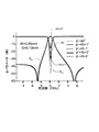
図16Aに、高周波信号の透過特性を示す。1段目のデュアルモードフィルタ150の共振周波数f1の近傍、及び2段目のデュアルモードフィルタ151の共振周波数f2の近傍において、高周波信号が減衰している。
FIG. 16A shows the transmission characteristics of the high-frequency signal. High-frequency signals are attenuated in the vicinity of the resonance frequency f 1 of the first-stage
図16Bに、入力信号と、出力信号との、スペクトルの関係を示す。入力信号Sinのスペクトルは、共振周波数f1とf2との中間の中心周波数を持ち、共振周波数f1及びf2の近傍に、裾野を持つ。図15に示した第10の実施例によるデュアルモードフィルタを適用すると、共振周波数f1とf2との近傍で減衰するため、入力信号Sinの裾野の部分が減衰する。このため、出力信号Soutのスペクトルの広がり幅が、入力信号Sinのスペクトルの広がり幅よりも狭くなる。これにより、周波数軸上で隣接するチャネルへの信号漏れを抑制することができる。 FIG. 16B shows the spectral relationship between the input signal and the output signal. Spectrum of the input signal Sin has a middle of the center frequency of the resonance frequencies f 1 and f 2, in the vicinity of the resonance frequency f 1 and f 2, with the horizons. When the dual mode filter according to the tenth embodiment shown in FIG. 15 is applied, the base portion of the input signal Sin is attenuated because attenuation is performed in the vicinity of the resonance frequencies f 1 and f 2 . For this reason, the spectrum spread width of the output signal Sout is narrower than the spectrum spread width of the input signal Sin. As a result, signal leakage to adjacent channels on the frequency axis can be suppressed.
第1の実施例によるデュアルモードフィルタを用いる場合には、入力信号Sinの電力のほぼ全てが、リング共振器21を通過する。このため、リング共振器21の耐電力性を高めておく必要がある。これに対し、第10の実施例では、入力信号Sinの大部分は、主伝送線路100をそのまま伝搬し、出力端Toに達する。デュアルモードフィルタ150、151のリング共振器を通過する信号は、入力信号Sinのうち裾野の周波数成分のみである。このため、リング共振器に、耐電力性の低いものを用いることができる。
When the dual mode filter according to the first embodiment is used, almost all of the power of the input signal Sin passes through the
図17に、第11の実施例によるデュアルモードフィルタの誘電体基板20上の導電パターンを示す。
FIG. 17 shows a conductive pattern on the
図13に示した第9の実施例では、第1のリング共振器110と第2のリング共振器120とが線対称の平面形状を有し、同一の共振周波数を持っていた。第11の実施例では、第1のリング共振器110の線路長と、第2のリング共振器120の線路長とが異なる。このため、両者の共振周波数が異なる。
In the ninth embodiment shown in FIG. 13, the
具体的には、第1のリング共振器110の平面形状は、図13に示した第9の実施例によるデュアルモードフィルタの第1のリング共振器110の平面形状と同一である。第2のリング共振器120の4つの角部の曲率が、第1のリング共振器110の4つの角部の曲率よりも小さい。第2のリング共振器120の相対する直線部分の間隔は、第1のリング共振器110の相対する直線部分の間隔と等しい。このため、第2のリング共振器120の線路長が、第1のリング共振器110の線路長よりも長くなる。
Specifically, the planar shape of the
主伝送線路100と第2のリング共振器120との結合の強さは、主伝送線路100と第1のリング共振器110との結合の強さとほぼ等しい。さらに、第2の副伝送線路140と第2のリング共振器120との結合の強さは、第1の副伝送線路130と第1のリング共振器110との結合の強さとほぼ等しい。
The strength of coupling between the
第2のデュアルモード発生線路121の端部と、第2のリング共振器120との間隙が、第1のデュアルモード発生線路111と第1のリング共振器110との間隙と等しくなるように設計されている。このため、第2のデュアルモード発生線路121は、第1のデュアルモード発生線路111よりも長くなる。
The gap between the end of second dual
第1のリング共振器110の共振周波数の近傍の周波数成分は、第1の副伝送線路130に伝搬し、第2のリング共振器120の共振周波数の近傍の周波数成分は、第2の副伝送線路140に伝搬する。
The frequency component in the vicinity of the resonance frequency of the
図18に、各伝送線路を伝搬する信号の振幅のスペクトルのシミュレーション結果を示す。図18に示した実線S21は、出力端Toに出力される信号の振幅を示し、点線S11は、入力端Tiに戻ってくる反射波の振幅を示す。破線S31及び一点鎖線S41は、それぞれ第1の副伝送線路130及び第2の副伝送線路140の出力端子に出力される信号の振幅を示す。
FIG. 18 shows a simulation result of the spectrum of the amplitude of the signal propagating through each transmission line. A solid line S21 illustrated in FIG. 18 indicates the amplitude of the signal output to the output end To, and a dotted line S11 indicates the amplitude of the reflected wave returning to the input end Ti. A broken line S31 and an alternate long and short dash line S41 indicate the amplitudes of signals output to the output terminals of the first
透過特性S21は、図16Aに示した透過特性に近似しており、第1のリング共振器110の共振周波数の近傍、及び第2のリング共振器120の共振周波数の近傍において、高周波信号が減衰している。
The transmission characteristic S21 approximates the transmission characteristic shown in FIG. 16A, and the high-frequency signal is attenuated in the vicinity of the resonance frequency of the
以上実施例に沿って本発明を説明したが、本発明はこれらに制限されるものではない。例えば、種々の変更、改良、組み合わせ等が可能なことは当業者に自明であろう。 Although the present invention has been described with reference to the embodiments, the present invention is not limited thereto. It will be apparent to those skilled in the art that various modifications, improvements, combinations, and the like can be made.
上記実施例1〜8に基づき、以下の付記に示された発明を開示する。 Based on Examples 1 to 8 above, the invention shown in the following supplementary notes is disclosed.
(付記1)
伝送線路をリング状にしたリング共振器と、
前記リング共振器上の第1の結合点において、該リング共振器に電磁気的に結合する入力フィーダと、
前記リング共振器上の、前記第1の結合点とは異なる第2の結合点において、該リング共振器に電磁気的に結合する出力フィーダと、
前記リング共振器の内側に配置され、該リング共振器上の第3の結合点において、一方の端部が該リング共振器に容量結合し、該第3の結合点から該リング共振器の線路長の1/2の長さだけ離れた第4の結合点において、他方の端部が該リング共振器に容量結合するデュアルモード発生線路と
を有するデュアルモードフィルタ。
(Appendix 1)
A ring resonator having a ring-shaped transmission line;
An input feeder electromagnetically coupled to the ring resonator at a first coupling point on the ring resonator;
An output feeder that electromagnetically couples to the ring resonator at a second coupling point on the ring resonator that is different from the first coupling point;
The ring resonator is disposed inside the ring resonator, and at a third coupling point on the ring resonator, one end is capacitively coupled to the ring resonator, and the line of the ring resonator is coupled from the third coupling point. A dual mode filter having a dual mode generation line whose other end is capacitively coupled to the ring resonator at a fourth coupling point separated by a length of ½.
(付記2)
前記第1の結合点から前記第2の結合点までの前記リング共振器の線路長が、該リング共振器の線路長の1/4である付記1に記載のデュアルモードフィルタ。
(Appendix 2)
The dual mode filter according to
(付記3)
前記第1の結合点から前記第2の結合点までの前記リング共振器の線路長が、該リング共振器の線路長の1/8または3/8である付記1に記載のデュアルモードフィルタ。
(Appendix 3)
The dual mode filter according to
(付記4)
前記第3の結合点は、前記第1の結合点と前記第2の結合点とを両端とする伝送線路の中点、または該中点からの線路長が前記リング共振器の線路長の1.4%以下の点に位置する付記1乃至3のいずれか1項に記載のデュアルモードフィルタ。
(Appendix 4)
The third coupling point is a midpoint of a transmission line having both ends of the first coupling point and the second coupling point, or a line length from the midpoint is 1 of the line length of the ring resonator. The dual mode filter according to any one of
(付記5)
前記第3の結合点は、前記第1の結合点と前記第2の結合点とを両端とする伝送線路の中点から、前記リング共振器の線路長の1/4の長さだけ離れた第1の点、または該第1の点からの線路長が前記リング共振器の線路長の1.4%以下の点に位置する付記1乃至3のいずれか1項に記載のデュアルモードフィルタ。
(Appendix 5)
The third coupling point is separated from the midpoint of the transmission line having both ends of the first coupling point and the second coupling point by a length ¼ of the line length of the ring resonator. The dual mode filter according to any one of
(付記6)
さらに、前記第3の結合点における前記リング共振器と前記デュアルモード発生線路との結合容量、及び前記第4の結合点における前記リング共振器と前記デュアルモード発生線路との結合容量の少なくとも一方を変化させる容量調整部材を有する付記1乃至5のいずれか1項に記載のデュアルモードフィルタ。
(Appendix 6)
Further, at least one of a coupling capacitance between the ring resonator and the dual mode generation line at the third coupling point and a coupling capacitance between the ring resonator and the dual mode generation line at the fourth coupling point is provided. The dual mode filter according to any one of
(付記7)
さらに、
第1の表面と第2の表面とを有する誘電体基板と、
前記誘電体基板の前記第1の表面に形成されたグランド膜と
を含み、
前記リング共振器、前記入力フィーダ、前記出力フィーダ、及び前記デュアルモード発生線路が、前記誘電体基板の前記第2の表面に形成された導電パターンを含む付記1乃至6のいずれか1項に記載のデュアルモードフィルタ。
(Appendix 7)
further,
A dielectric substrate having a first surface and a second surface;
A ground film formed on the first surface of the dielectric substrate,
The ring resonator, the input feeder, the output feeder, and the dual-mode generation line include any one of
(付記8)
入力端から出路端まで延在する主伝送線路と、
前記主伝送線路の脇に配置され、該主伝送線路に電磁気的に結合する第1のリング共振器と、
前記第1のリング共振器に、前記主伝送線路とは異なる箇所において電磁気的に結合する第1の副伝送線路と、
前記第1のリング共振器の内側に配置され、該第1のリング共振器上の第1の結合点において、一方の端部が該第1のリング共振器に容量結合し、該第1の結合点から該第1のリング共振器の線路長の1/2の長さだけ離れた第2の結合点において、他方の端部が該第1のリング共振器に容量結合する第1のデュアルモード発生線路と
を有するデュアルモードフィルタ。
(Appendix 8)
A main transmission line extending from the input end to the output end;
A first ring resonator disposed beside the main transmission line and electromagnetically coupled to the main transmission line;
A first subtransmission line that is electromagnetically coupled to the first ring resonator at a location different from the main transmission line;
The first ring resonator is disposed inside the first ring resonator, and one end thereof is capacitively coupled to the first ring resonator at a first coupling point on the first ring resonator. A first dual in which the other end is capacitively coupled to the first ring resonator at a second coupling point that is one-half the line length of the first ring resonator from the coupling point. A dual mode filter having a mode generation line.
(付記9)
前記第1の副伝送線路の延在する方向は、前記主伝送線路の延在する方向と直交する付記8に記載のデュアルモードフィルタ。
(Appendix 9)
The dual mode filter according to
(付記10)
さらに、
前記主伝送線路の脇に配置され、該主伝送線路に電磁気的に結合し、前記第1のリング共振器とは異なる共振周波数を持つ第2のリング共振器と、
前記第2のリング共振器に、前記主伝送線路とは異なる箇所において電磁気的に結合する第2の副伝送線路と、
前記第2のリング共振器の内側に配置され、該第2のリング共振器上の第3の結合点において、一方の端部が該第2のリング共振器に容量結合し、該第3の結合点から該第2のリング共振器の線路長の1/2の長さだけ離れた第4の結合点において、他方の端部が該第2のリング共振器に容量結合する第2のデュアルモード発生線路と
を有する付記8または9に記載のデュアルモードフィルタ。
(Appendix 10)
further,
A second ring resonator disposed beside the main transmission line, electromagnetically coupled to the main transmission line, and having a resonance frequency different from that of the first ring resonator;
A second sub-transmission line that is electromagnetically coupled to the second ring resonator at a location different from the main transmission line;
Arranged at the inside of the second ring resonator, and at a third coupling point on the second ring resonator, one end is capacitively coupled to the second ring resonator, and the third ring resonator A second dual in which the other end is capacitively coupled to the second ring resonator at a fourth coupling point separated from the coupling point by ½ of the line length of the second ring resonator. The dual mode filter according to
(付記11)
前記第2の副伝送線路の延在する方向は、前記主伝送線路の延在する方向と直交する付記10に記載のデュアルモードフィルタ。
(Appendix 11)
The dual mode filter according to
(付記12)
前記第1のリング共振器と前記第2のリング共振器とが、相互に異なる箇所において前記主伝送線路に結合する付記10または11に記載のデュアルモードフィルタ。
(Appendix 12)
The dual mode filter according to
(付記13)
前記第1のリング共振器と前記第2のリング共振器とが、前記主伝送線路の同一箇所において該主伝送線路に結合し、前記第1のリング共振器と前記第2のリング共振器とは、前記主伝送線路の相互に異なる側に配置されている付記10または11に記載のデュアルモードフィルタ。
(Appendix 13)
The first ring resonator and the second ring resonator are coupled to the main transmission line at the same location of the main transmission line, and the first ring resonator and the second ring resonator are These are the dual mode filters of
(付記14)
さらに、
第1の表面と第2の表面とを有する誘電体基板と、
前記誘電体基板の前記第1の表面に形成されたグランド膜と
を含み、
前記主伝送線路、前記第1のリング共振器、前記第1の副伝送線路、及び前記第1の主アルモード発生線路が、前記誘電体基板の前記第2の表面に形成された導電パターンを含む付記8乃至13のいずれか1項に記載のデュアルモードフィルタ。
(Appendix 14)
further,
A dielectric substrate having a first surface and a second surface;
A ground film formed on the first surface of the dielectric substrate,
The main transmission line, the first ring resonator, the first sub-transmission line, and the first main al-mode generation line are conductive patterns formed on the second surface of the dielectric substrate. 14. The dual mode filter according to any one of
(付記15)
さらに、
第1の表面と第2の表面とを有する誘電体基板と、
前記誘電体基板の前記第1の表面に形成されたグランド膜と
を含み、
前記主伝送線路、前記第1のリング共振器、前記第2のリング共振器、前記第1の副伝送線路、前記第2の副伝送線路、及び前記第1の主アルモード発生線路が、前記誘電体基板の前記第2の表面に形成された導電パターンを含む付記10乃至13のいずれか1項に記載のデュアルモードフィルタ。
(Appendix 15)
further,
A dielectric substrate having a first surface and a second surface;
A ground film formed on the first surface of the dielectric substrate,
The main transmission line, the first ring resonator, the second ring resonator, the first sub transmission line, the second sub transmission line, and the first main almode generation line are 14. The dual mode filter according to any one of
15 パッケージ
20 誘電体基板
21 リング共振器
22 入力フィーダ
23 出力フィーダ
24 デュアルモード発生線路
27 グランド膜
35 入力コネクタ
36 出力コネクタ
60 誘電体基板
61 グランド膜
71 第1の誘電体部材
72 第2の誘電体部材
73 第1の支持部材
74 第2の支持部材
100 主伝送線路
110 第1のリング共振器
111 第1のデュアルモード発生線路
120 第2のリング共振器
121 第2のデュアルモード発生線路
130 第1の副伝送線路
131 第1の終端抵抗
140 第2の副伝送線路
141 第2の終端抵抗
150 1段目デュアルモードフィルタ
151 2段目デュアルモードフィルタ
P1〜P6 結合点
Ti 入力端
To 出力端
15
Claims (10)
前記リング共振器上の第1の結合点において、該リング共振器に電磁気的に結合する入力フィーダと、
前記リング共振器上の、前記第1の結合点とは異なる第2の結合点において、該リング共振器に電磁気的に結合する出力フィーダと、
前記リング共振器の内側に配置され、該リング共振器上の第3の結合点において、一方の端部が該リング共振器に容量結合し、該第3の結合点から該リング共振器の線路長の1/2の長さだけ離れた第4の結合点において、他方の端部が該リング共振器に容量結合するデュアルモード発生線路と
を有するデュアルモードフィルタ。 A ring resonator having a ring-shaped transmission line;
An input feeder electromagnetically coupled to the ring resonator at a first coupling point on the ring resonator;
An output feeder that electromagnetically couples to the ring resonator at a second coupling point on the ring resonator that is different from the first coupling point;
The ring resonator is disposed inside the ring resonator, and at a third coupling point on the ring resonator, one end is capacitively coupled to the ring resonator, and the line of the ring resonator is coupled from the third coupling point. A dual mode filter having a dual mode generation line whose other end is capacitively coupled to the ring resonator at a fourth coupling point separated by a length of ½.
第1の表面と第2の表面とを有する誘電体基板と、
前記誘電体基板の前記第1の表面に形成されたグランド膜と
を含み、
前記リング共振器、前記入力フィーダ、前記出力フィーダ、及び前記デュアルモード発生線路が、前記誘電体基板の前記第2の表面に形成された導電パターンを含む請求項1乃至4のいずれか1項に記載のデュアルモードフィルタ。 further,
A dielectric substrate having a first surface and a second surface;
A ground film formed on the first surface of the dielectric substrate,
5. The ring resonator according to claim 1, wherein the ring resonator, the input feeder, the output feeder, and the dual mode generation line include a conductive pattern formed on the second surface of the dielectric substrate. The dual mode filter described.
前記主伝送線路の脇に配置され、該主伝送線路に電磁気的に結合する第1のリング共振器と、
前記第1のリング共振器に、前記主伝送線路とは異なる箇所において電磁気的に結合する第1の副伝送線路と、
前記第1のリング共振器の内側に配置され、該第1のリング共振器上の第1の結合点において、一方の端部が該第1のリング共振器に容量結合し、該第1の結合点から該第1のリング共振器の線路長の1/2の長さだけ離れた第2の結合点において、他方の端部が該第1のリング共振器に容量結合する第1のデュアルモード発生線路と
を有するデュアルモードフィルタ。 A main transmission line extending from the input end to the output end;
A first ring resonator disposed beside the main transmission line and electromagnetically coupled to the main transmission line;
A first subtransmission line that is electromagnetically coupled to the first ring resonator at a location different from the main transmission line;
The first ring resonator is disposed inside the first ring resonator, and one end thereof is capacitively coupled to the first ring resonator at a first coupling point on the first ring resonator. A first dual in which the other end is capacitively coupled to the first ring resonator at a second coupling point that is one-half the line length of the first ring resonator from the coupling point. A dual mode filter having a mode generation line.
前記主伝送線路の脇に配置され、該主伝送線路に電磁気的に結合し、前記第1のリング共振器とは異なる共振周波数を持つ第2のリング共振器と、
前記第2のリング共振器に、前記主伝送線路とは異なる箇所において電磁気的に結合する第2の副伝送線路と、
前記第2のリング共振器の内側に配置され、該第2のリング共振器上の第3の結合点において、一方の端部が該第2のリング共振器に容量結合し、該第3の結合点から該第2のリング共振器の線路長の1/2の長さだけ離れた第4の結合点において、他方の端部が該第2のリング共振器に容量結合する第2のデュアルモード発生線路と
を有する請求項6または7に記載のデュアルモードフィルタ。 further,
A second ring resonator disposed beside the main transmission line, electromagnetically coupled to the main transmission line, and having a resonance frequency different from that of the first ring resonator;
A second sub-transmission line that is electromagnetically coupled to the second ring resonator at a location different from the main transmission line;
Arranged at the inside of the second ring resonator, and at a third coupling point on the second ring resonator, one end is capacitively coupled to the second ring resonator, and the third ring resonator A second dual in which the other end is capacitively coupled to the second ring resonator at a fourth coupling point separated from the coupling point by ½ of the line length of the second ring resonator. The dual mode filter according to claim 6, further comprising a mode generation line.
Priority Applications (2)
| Application Number | Priority Date | Filing Date | Title |
|---|---|---|---|
| JP2008332782A JP5062165B2 (en) | 2008-06-18 | 2008-12-26 | Dual mode filter |
| US12/411,584 US7978028B2 (en) | 2008-06-18 | 2009-03-26 | Dual mode generating line coupled to a dual mode ring resonator filter by half the length of the ring resonator |
Applications Claiming Priority (3)
| Application Number | Priority Date | Filing Date | Title |
|---|---|---|---|
| JP2008159092 | 2008-06-18 | ||
| JP2008159092 | 2008-06-18 | ||
| JP2008332782A JP5062165B2 (en) | 2008-06-18 | 2008-12-26 | Dual mode filter |
Publications (2)
| Publication Number | Publication Date |
|---|---|
| JP2010028787A true JP2010028787A (en) | 2010-02-04 |
| JP5062165B2 JP5062165B2 (en) | 2012-10-31 |
Family
ID=41430618
Family Applications (1)
| Application Number | Title | Priority Date | Filing Date |
|---|---|---|---|
| JP2008332782A Active JP5062165B2 (en) | 2008-06-18 | 2008-12-26 | Dual mode filter |
Country Status (2)
| Country | Link |
|---|---|
| US (1) | US7978028B2 (en) |
| JP (1) | JP5062165B2 (en) |
Families Citing this family (2)
| Publication number | Priority date | Publication date | Assignee | Title |
|---|---|---|---|---|
| CN102361117B (en) * | 2011-09-29 | 2014-04-02 | 武汉虹信通信技术有限责任公司 | Capacitive cross coupling flying bar and coaxial cavity resonator thereof |
| CN103915672B (en) * | 2014-04-08 | 2016-05-04 | 山东国恒机电配套有限公司 | A kind of dicyclo 3dB electric bridge |
Citations (6)
| Publication number | Priority date | Publication date | Assignee | Title |
|---|---|---|---|---|
| JPS6399601A (en) * | 1986-06-26 | 1988-04-30 | Nec Corp | Microwave band equalizer |
| JPH07249901A (en) * | 1994-03-09 | 1995-09-26 | Matsushita Electric Ind Co Ltd | High frequency filter |
| JPH0856107A (en) * | 1994-08-11 | 1996-02-27 | Matsushita Electric Ind Co Ltd | Dual mode resonator |
| JPH11136013A (en) * | 1997-10-29 | 1999-05-21 | Matsushita Electric Ind Co Ltd | Band passing device |
| JP2000209002A (en) * | 1999-01-19 | 2000-07-28 | Matsushita Electric Ind Co Ltd | Dual mode filter |
| JP2006101187A (en) * | 2004-09-29 | 2006-04-13 | Fujitsu Ltd | Superconducting device |
Family Cites Families (3)
| Publication number | Priority date | Publication date | Assignee | Title |
|---|---|---|---|---|
| US5400002A (en) * | 1992-06-12 | 1995-03-21 | Matsushita Electric Industrial Co., Ltd. | Strip dual mode filter in which a resonance width of a microwave is adjusted and dual mode multistage filter in which the strip dual mode filters are arranged in series |
| JP3304724B2 (en) | 1995-11-16 | 2002-07-22 | 松下電器産業株式会社 | Dual mode filter |
| US7902945B2 (en) * | 2007-05-21 | 2011-03-08 | Fujitsu Limited | Dual mode ring resonator filter with a dual mode generating line disposed inside the ring resonator |
-
2008
- 2008-12-26 JP JP2008332782A patent/JP5062165B2/en active Active
-
2009
- 2009-03-26 US US12/411,584 patent/US7978028B2/en active Active
Patent Citations (6)
| Publication number | Priority date | Publication date | Assignee | Title |
|---|---|---|---|---|
| JPS6399601A (en) * | 1986-06-26 | 1988-04-30 | Nec Corp | Microwave band equalizer |
| JPH07249901A (en) * | 1994-03-09 | 1995-09-26 | Matsushita Electric Ind Co Ltd | High frequency filter |
| JPH0856107A (en) * | 1994-08-11 | 1996-02-27 | Matsushita Electric Ind Co Ltd | Dual mode resonator |
| JPH11136013A (en) * | 1997-10-29 | 1999-05-21 | Matsushita Electric Ind Co Ltd | Band passing device |
| JP2000209002A (en) * | 1999-01-19 | 2000-07-28 | Matsushita Electric Ind Co Ltd | Dual mode filter |
| JP2006101187A (en) * | 2004-09-29 | 2006-04-13 | Fujitsu Ltd | Superconducting device |
Also Published As
| Publication number | Publication date |
|---|---|
| JP5062165B2 (en) | 2012-10-31 |
| US20090315647A1 (en) | 2009-12-24 |
| US7978028B2 (en) | 2011-07-12 |
Similar Documents
| Publication | Publication Date | Title |
|---|---|---|
| US7902945B2 (en) | Dual mode ring resonator filter with a dual mode generating line disposed inside the ring resonator | |
| JP6265461B2 (en) | Resonator-loaded dual-band resonator and dual-band filter using the same | |
| JPH09139612A (en) | Dual mode filter | |
| US8942774B2 (en) | Radio-frequency filter comprising an even mode resonance of a same phase inside the bandwidth and an odd mode resonance of a reverse phase outside the bandwidth | |
| JP2007005951A (en) | Transmission circuit, antenna duplexer, high frequency switch circuit | |
| JP4778011B2 (en) | High frequency filter | |
| JP2007318661A (en) | Bandpass filter, high frequency module using the same and radio communication device using the same | |
| JP4728994B2 (en) | Coplanar resonator and coplanar filter using the same | |
| JP5062165B2 (en) | Dual mode filter | |
| US6184760B1 (en) | Half-wavelength resonator type high frequency filter | |
| JP2014236362A (en) | Dual band resonator and dual band pass filter using the same | |
| JP2014036258A (en) | Multiband band-pass filter | |
| JP5369905B2 (en) | Band elimination filter | |
| JP2000013106A (en) | Dielectric filter, shared transmitter/receiver sharing unit and communication equipment | |
| US7970447B2 (en) | High frequency filter having a solid circular shape resonance pattern with multiple input/output ports and an inter-port waveguide connecting corresponding output and input ports | |
| JP4769830B2 (en) | Dual mode filter and tuning method | |
| JP4189971B2 (en) | Variable frequency type high frequency filter | |
| JP5606199B2 (en) | Filter device | |
| JP4789850B2 (en) | Band pass filter and method for manufacturing the same | |
| JP2009044206A (en) | Antenna structure | |
| JPH07183710A (en) | Dielectric resonator and its input/output coupling circuit | |
| JP2006238213A (en) | High frequency filter using coplanar line resonator | |
| JP7425717B2 (en) | Filter and wireless transmitter | |
| JP2004289755A (en) | High frequency filter control method, high frequency filter manufacturing method, and high frequency filter | |
| JP4769753B2 (en) | Superconducting filter device |
Legal Events
| Date | Code | Title | Description |
|---|---|---|---|
| A621 | Written request for application examination |
Free format text: JAPANESE INTERMEDIATE CODE: A621 Effective date: 20110513 |
|
| A977 | Report on retrieval |
Free format text: JAPANESE INTERMEDIATE CODE: A971007 Effective date: 20120607 |
|
| TRDD | Decision of grant or rejection written | ||
| A01 | Written decision to grant a patent or to grant a registration (utility model) |
Free format text: JAPANESE INTERMEDIATE CODE: A01 Effective date: 20120710 |
|
| A01 | Written decision to grant a patent or to grant a registration (utility model) |
Free format text: JAPANESE INTERMEDIATE CODE: A01 |
|
| A61 | First payment of annual fees (during grant procedure) |
Free format text: JAPANESE INTERMEDIATE CODE: A61 Effective date: 20120723 |
|
| R150 | Certificate of patent or registration of utility model |
Ref document number: 5062165 Country of ref document: JP Free format text: JAPANESE INTERMEDIATE CODE: R150 Free format text: JAPANESE INTERMEDIATE CODE: R150 |
|
| FPAY | Renewal fee payment (event date is renewal date of database) |
Free format text: PAYMENT UNTIL: 20150817 Year of fee payment: 3 |