JP2010027611A - Fit-in inductive proximity sensor and its design method - Google Patents
Fit-in inductive proximity sensor and its design method Download PDFInfo
- Publication number
- JP2010027611A JP2010027611A JP2009165731A JP2009165731A JP2010027611A JP 2010027611 A JP2010027611 A JP 2010027611A JP 2009165731 A JP2009165731 A JP 2009165731A JP 2009165731 A JP2009165731 A JP 2009165731A JP 2010027611 A JP2010027611 A JP 2010027611A
- Authority
- JP
- Japan
- Prior art keywords
- sensor
- proximity sensor
- core
- attenuation
- sleeve
- Prior art date
- Legal status (The legal status is an assumption and is not a legal conclusion. Google has not performed a legal analysis and makes no representation as to the accuracy of the status listed.)
- Granted
Links
Images


Classifications
-
- H—ELECTRICITY
- H03—ELECTRONIC CIRCUITRY
- H03K—PULSE TECHNIQUE
- H03K17/00—Electronic switching or gating, i.e. not by contact-making and –breaking
- H03K17/94—Electronic switching or gating, i.e. not by contact-making and –breaking characterised by the way in which the control signals are generated
- H03K17/945—Proximity switches
- H03K17/95—Proximity switches using a magnetic detector
- H03K17/9505—Constructional details
-
- H—ELECTRICITY
- H03—ELECTRONIC CIRCUITRY
- H03K—PULSE TECHNIQUE
- H03K17/00—Electronic switching or gating, i.e. not by contact-making and –breaking
- H03K17/94—Electronic switching or gating, i.e. not by contact-making and –breaking characterised by the way in which the control signals are generated
- H03K17/945—Proximity switches
- H03K17/95—Proximity switches using a magnetic detector
- H03K17/9502—Measures for increasing reliability
-
- H—ELECTRICITY
- H03—ELECTRONIC CIRCUITRY
- H03K—PULSE TECHNIQUE
- H03K17/00—Electronic switching or gating, i.e. not by contact-making and –breaking
- H03K17/94—Electronic switching or gating, i.e. not by contact-making and –breaking characterised by the way in which the control signals are generated
- H03K17/945—Proximity switches
- H03K17/95—Proximity switches using a magnetic detector
- H03K17/952—Proximity switches using a magnetic detector using inductive coils
- H03K17/9537—Proximity switches using a magnetic detector using inductive coils in a resonant circuit
- H03K17/9542—Proximity switches using a magnetic detector using inductive coils in a resonant circuit forming part of an oscillator
- H03K17/9547—Proximity switches using a magnetic detector using inductive coils in a resonant circuit forming part of an oscillator with variable amplitude
Landscapes
- Switches That Are Operated By Magnetic Or Electric Fields (AREA)
- Measurement Of Length, Angles, Or The Like Using Electric Or Magnetic Means (AREA)
Abstract
Description
本発明は請求項1または9の前文に記載された金属取付板に嵌め込む誘導近接センサおよびその設計方法に関連する。
The present invention relates to an inductive proximity sensor that fits into a metal mounting plate as described in the preamble of
近接センサはセンサコイル付きRLC発振器を含み、その磁界はターゲット内に渦電流を生じる。これらの渦電流により生じる電力損失はセンサとターゲット間の距離が減少するにつれ発振器を漸次減衰させる負荷を現わす。 The proximity sensor includes an RLC oscillator with a sensor coil whose magnetic field produces eddy currents in the target. The power loss caused by these eddy currents presents a load that gradually attenuates the oscillator as the distance between the sensor and target decreases.
発振器がその蓄積エネルギを消散させる割合の測度は品質係数Qであり、それはサイクル当たり消散エネルギに対する蓄積エネルギの比の2π倍である。誘導近接センサの発振システムの最大品質係数Qmaxはセンサの非嵌込状態においてターゲットが存在しない時に測定される。作動において、品質係数Qは取付板および/またはターゲット内の渦電流損失により低下する。品質係数Qを最大品質係数Qmaxに正規化して、相対的品質係数Qrelが次のように定義される。

センサの環境内に磁界影響体が存在しなければ、QはQmaxに等しくしたがってQrelは1に等しい。品質係数Qに関して前記したことは相対的品質係数Qrelにも当てはまり、それは取付板および/またはターゲット内の渦電流損失によりサイクル当たり消散エネルギが増加する事実により低下する。この低下量は発振器の減衰の測度である。
センサ回路はこの減衰の関数である出力信号を発生するようにされた測定回路を含んでいる。 The sensor circuit includes a measurement circuit adapted to generate an output signal that is a function of this attenuation.
スイッチングおよびアナログ誘導近接センサは区別される。近接スイッチの測定回路は減衰が、ここでは動作閾値とも呼ばれる、基準閾値に達するとすぐに出力信号を1つの状態からもう1つの状態へ切り替えるようにされているが、アナログ近接センサの測定回路は、基準閾値を超える減衰に対しては、発振器減衰の単調関数である出力信号を発生するようにされている。 Switching and analog inductive proximity sensors are distinguished. The proximity switch measurement circuit is designed to switch the output signal from one state to the other as soon as the attenuation reaches a reference threshold, also referred to herein as the operating threshold. For attenuation above a reference threshold, an output signal that is a monotonic function of oscillator attenuation is generated.
センサの筺体の外面はコアによりセンサコイルの磁界がそこへ向けられるセンシング面(sensing face)を含んでいる。ターゲット距離はこのセンシング面からターゲットまでの距離であり、センサの範囲はセンサの出力信号に変化を生じるためにこのターゲット距離を減少させる(ターゲットをセンシング面に近づけて)必要がある値である。このように定義されるセンサ範囲はセンサが近接スイッチであれば動作範囲と呼ばれる。センサのデータシート内に明記された範囲は定格範囲と呼ばれる。センサの実際の範囲は、たとえば、製造公差によりその定格範囲を逸脱することがある。 The outer surface of the sensor housing includes a sensing face through which the magnetic field of the sensor coil is directed by the core. The target distance is the distance from the sensing surface to the target, and the range of the sensor is a value that needs to be reduced (to bring the target closer to the sensing surface) in order to cause a change in the output signal of the sensor. The sensor range defined in this way is called an operation range if the sensor is a proximity switch. The range specified in the sensor data sheet is called the rated range. The actual range of the sensor may deviate from its rated range due to manufacturing tolerances, for example.
センサ範囲の測定および明記の基礎として、国際標準IEC60947−5−2は使用すべきターゲットの材料を規定している。標準ターゲットは厚さが1mmで側面の長さがセンシング面の直径またはセンサの定格範囲の3倍の、どちらか大きい方に等しい正方形の軟鋼板である。 As a basis for measuring and specifying the sensor range, the international standard IEC 60947-5-2 defines the target material to be used. The standard target is a square mild steel plate having a thickness of 1 mm and a side length equal to the larger of the diameter of the sensing surface or three times the rated range of the sensor, whichever is greater.
誘導近接センサの範囲とその嵌込可能性は逆関係にある。ターゲット距離が大きいほどターゲット内の渦電流損は小さく、発振器減衰に対して決定される渦電流損の総量に対する取付板内の渦電流損のインパクトが増大する。 The range of the inductive proximity sensor and its insertion possibility are inversely related. The larger the target distance, the smaller the eddy current loss in the target, and the impact of the eddy current loss in the mounting plate on the total amount of eddy current loss determined for oscillator damping increases.
センサの範囲を拡大するために、その基準閾値が低減される。下記の表において、およそ35%の基準閾値により得られる標準IEC60947−5−2に明記されている嵌込可能近接スイッチの定格動作距離が僅か10%の基準閾値により特徴づけられる対応するサイズの先端技術の近接スイッチの測定された動作距離と比較される。
この表において、センサのサイズはセンサの筺体を形成する外側にねじが切られたスリーブの直径により明記される。 In this table, the size of the sensor is specified by the diameter of the outer threaded sleeve that forms the sensor housing.
長距離近接センサは10%以下の基準閾値により特徴づけられる。基準閾値を10%よりも低く低減することにより、さらに長距離のセンサを実現することができる。5%よりも低い基準閾値を有する長距離センサが従来技術で知られている。前記した表の右列内の値に基づいて、長距離センサの最少範囲Sminは次式を使用して近似的に求めることができ、
![]()
ここに、dはセンサの筺体スリーブの外径(mm)であり、Sminはセンサ範囲(mm)である。
Long range proximity sensors are characterized by a reference threshold of 10% or less. By reducing the reference threshold value to be lower than 10%, a sensor having a longer distance can be realized. Long distance sensors with a reference threshold lower than 5% are known in the prior art. Based on the values in the right column of the table above, the minimum range S min of the long-range sensor can be approximately determined using the following equation:
![]()
Here, d is the outer diameter (mm) of the housing sleeve of the sensor, and S min is the sensor range (mm).
嵌込状態の取付板により生じる減衰はセンサの基準閾値とほぼ一致するかまたはそれを超えるため、通常の長距離センサは鋼取付板内に完全に嵌め込むことはできず、特に、任意のスイッチング型近接センサを作動不能とする。 Because the attenuation caused by the fitted mounting plate almost matches or exceeds the sensor's reference threshold, a normal long-range sensor cannot fit completely into the steel mounting plate, especially any switching The mold proximity sensor is disabled.
取付板の影響を緩和するために、コイルおよびコアを取り囲むシールド・スカートを使用してセンサ磁界が取付板に達するのを防止することが特許文献1で示唆されている。交番磁界に対してシールドとして作用するように設計された金属層は磁界の発振周波数において層材料の表皮深さと少なくとも同じ厚さであり、好ましくはそれより厚い。材料の表皮深さは次式から計算することができ、
ここに、ρは材料の抵抗率[Ω・m]、
fは磁界の角周波数[Hz]、
μ0は自由空間の透磁率[N/A2]、
μrは材料の比透磁率である。
In order to mitigate the effects of the mounting plate, it is suggested in US Pat. No. 6,057,077 that a shield skirt surrounding the coil and core is used to prevent the sensor magnetic field from reaching the mounting plate. A metal layer designed to act as a shield against an alternating magnetic field is at least as thick as the skin depth of the layer material at the oscillation frequency of the magnetic field, and is preferably thicker. The skin depth of the material can be calculated from
Where ρ is the resistivity of the material [Ω · m],
f is the angular frequency [Hz] of the magnetic field,
μ 0 is the permeability [N / A 2 ] of free space,
μ r is the relative permeability of the material.
たとえば、1MHzの周波数における銅の表皮深さは66μmである。コア付センサコイルを有するセンサの動作周波数は長い動作距離に達するために好ましくは50kHzよりも高いが、それは一般的には1MHzよりも低く、したがって、コアを取り囲む銅層はシールドとして作用するためにより厚くなければならない。 For example, the skin depth of copper at a frequency of 1 MHz is 66 μm. The operating frequency of a sensor with a cored sensor coil is preferably higher than 50 kHz in order to reach a longer operating distance, but it is generally lower than 1 MHz, so the copper layer surrounding the core is more likely to act as a shield. Must be thick.
センサ範囲に逆影響を及ぼすことなく近接センサの嵌込可能性を改善することが本発明の目的である。 It is an object of the present invention to improve the proximity of a proximity sensor without adversely affecting the sensor range.
この目的は請求項1または9記載の嵌込可能近接センサおよび請求項13または14記載のこのようなセンサの設計方法により達成される。 This object is achieved by an insertable proximity sensor according to claim 1 or 9 and a method for designing such a sensor according to claim 13 or 14.
本発明の好ましい特徴は従属項に明記されている。 Preferred features of the invention are specified in the dependent claims.
以下に、添付図に示す好ましい実施例と共に本発明が詳細に説明される。 In the following, the invention will be described in detail in conjunction with a preferred embodiment shown in the accompanying drawings.
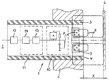
図1は取付板2内に取り付けられた誘導近接センサ1を示す図である。センサの筺体は実質的に非強磁性金属で作られた円筒スリーブ3からなり、それは外側がねじ切りされて取付板2の対応するねじ切り貫通孔内へねじ込まれ、スリーブ軸に垂直な筺体のセンシング面4が取付板2の前面5と同一平面となるようにされる。同一平面取付という用語は以後嵌込の同義語として使用され、取付板の貫通孔は取付板の前面5近くで拡大されず、センサ1の前部周りにスペースは提供されないことを意味する。
FIG. 1 is a view showing an
図2は図1に従って取付板2内に取り付けられた誘導近接センサ1およびそのセンシング面4の前に配置されたターゲット板6を含む構成の略図である。センサは電気回路および磁気回路を有し、それらは別々に示されている。センサコイル7を有する電気回路がブロック図として示されており、磁気回路は磁界線8および磁界に露呈される材料の異なる本体、すなわち、センサコイル7のオープン・ポット・コア9、このコア9を半径方向に取り囲む筺体スリーブ3、取付板2およびターゲット6により表わされる。これらの本体は円筒形で円形断面のスリーブ3の中央を通る切断面で断面図として示される。電気回路および磁気回路はセンサコイル7によりリンクされる。
FIG. 2 is a schematic diagram of a configuration including an
センサ回路とも呼ばれる電気回路はRLC発振器10を含み、その誘導コンポーネントLはセンサコイル7およびこのコイルのコア9により形成される。コア9は1よりも大きい比透磁率を有する材料、典型的にはフェライト、により構成される。センサコイルの磁界はターゲット6内に渦電流を発生し、これらの渦電流により生じる電力損失は、ターゲット距離xと呼ばれる、センシング面4とターゲット6間の距離が減少するにつれ発振器10をますます減衰させる負荷を表す。
The electrical circuit, also called the sensor circuit, includes an
センサ回路は、さらに、測定回路11および出力回路12を含んでいる。測定回路11は減衰の単調関数である電気量に基づいて発振器減衰を測定するように設計される。発振器の電子的設計に応じて、この量は、たとえば、発振器の振幅または発振器の帰還増幅器の出力電流とすることができる。測定回路は信号変換ユニット14を含み、整流器13がそれに先行することができる。近接スイッチの信号変換ユニット14は減衰をここでは動作閾値とも呼ばれる予め定められた基準閾値と比較する比較器である。これに反して、アナログ近接センサの信号変換ユニット14はゼロと減衰が基準閾値に対応する距離との間の値に対するターゲット距離xの線形関数である測定回路の出力信号を発生するように設計された伝達関数を有する。 The sensor circuit further includes a measurement circuit 11 and an output circuit 12. The measurement circuit 11 is designed to measure oscillator attenuation based on an electrical quantity that is a monotonic function of attenuation. Depending on the electronic design of the oscillator, this amount can be, for example, the amplitude of the oscillator or the output current of the feedback amplifier of the oscillator. The measurement circuit includes a signal conversion unit 14, which can be preceded by a rectifier 13. The signal conversion unit 14 of the proximity switch is a comparator that compares the attenuation to a predetermined reference threshold, also referred to herein as the operating threshold. In contrast, the signal conversion unit 14 of the analog proximity sensor is designed to generate an output signal of the measurement circuit that is a linear function of the target distance x relative to a value between zero and a distance whose attenuation corresponds to a reference threshold. Have a transfer function.
信号変換ユニット14の出力信号は信号処理により筺体の外側で利用できるようにされるセンサの出力信号を形成するために出力回路12により調整される。 The output signal of the signal conversion unit 14 is adjusted by the output circuit 12 to form a sensor output signal that is made available outside the housing by signal processing.
標準サイズ・ターゲットが前記したように発振器を予め定められた基準閾値まで減衰させるターゲット距離xがセンサの範囲を規定する。スイッチング型のセンサの範囲は動作距離とも呼ばれる。 The target distance x that the standard size target attenuates the oscillator to a predetermined reference threshold as described above defines the sensor range. The range of the switching type sensor is also called the operating distance.
図3はターゲット距離の関数としての相対発振器減衰Qrelのグラフを示す。長距離センサの基準閾値は90%ラインよりも上である。この動作点において曲線はいくぶん平坦であり、取付板により生じる小さな減衰でもセンサ範囲に著しいインパクトを与える。それにもかかわらず、センサコイルのコアを半径方向に取り囲む導電要素のジオメトリおよび電気抵抗率は取付板内に嵌め込まれたセンサの範囲が非嵌込センサの範囲(取付板の無い同じセンサの範囲)に一致するように適合できるため、金属取付板(通常、軟鋼取付板)内に嵌込可能な長距離近接センサの設計が可能である。 FIG. 3 shows a graph of relative oscillator attenuation Q rel as a function of target distance. The long range sensor reference threshold is above the 90% line. At this operating point, the curve is somewhat flat and even small attenuation caused by the mounting plate has a significant impact on the sensor range. Nevertheless, the geometry and electrical resistivity of the conductive element that radially surrounds the core of the sensor coil is the range of the sensor fitted in the mounting plate is the range of the non-inserting sensor (the same sensor range without the mounting plate) Therefore, it is possible to design a long-distance proximity sensor that can be fitted into a metal mounting plate (usually a mild steel mounting plate).
このアライメント(一致)の精度が高いほど、センサの嵌込可能性が良くなる。嵌込可能と見なされる誘導近接センサに対して、嵌込状態でのその範囲は非嵌込状態でのその範囲から著しく違ってはならない。前者と後者間の30%よりも多い差は著しいと見なされる。好ましくはこの差は20%を超えず、より好ましくはこの差は10%を超えない。 The higher the accuracy of this alignment (matching), the better the possibility that the sensor will be fitted. For an inductive proximity sensor that is considered to be insertable, its range in the inserted state should not differ significantly from its range in the non-inserted state. A difference of more than 30% between the former and the latter is considered significant. Preferably this difference does not exceed 20%, more preferably this difference does not exceed 10%.
導電要素は筺体の一部を形成したり筺体内に配置したりすることができる。通常、センサコイルのコアを取り囲む導電要素の1つは筺体の金属スリーブ3である。さらなる要素はこのようなスリーブまたはコアとスリーブ間に半径方向に配置される1つ以上の要素の内面および/または外面に施される金属層を含むことができる。
The conductive element can form part of the housing or be placed in the housing. Typically, one of the conductive elements surrounding the sensor coil core is a
コアを半径方向に取り囲む要素は半径方向でコアの外側にありしかも軸方向でコアに近い要素であり、それらはセンサの嵌込および/または非嵌込状態においてセンサコイルの磁界に少なくとも一部露呈される。コアは磁界を筺体の前端へ向けるため、軸方向において、これは部分的または全体的にコアの前にある要素を含む。逆に、磁界に露呈されずかつ渦電流を通さないスリーブ3の後部のジオメトリはセンサ・ターゲット構成内の渦電流損に影響を及ぼさない。したがって、コアを取り囲む中空円筒金属部材を表すスリーブの前部はコアを取り囲む導電要素と見なされる。一般的な原則として、コアの後端の後ろにあるものは全て無視することができる。
The elements that radially surround the core are those that are radially outside the core and close to the core in the axial direction, and they are at least partially exposed to the magnetic field of the sensor coil in the inserted and / or uninserted state of the sensor. Is done. Since the core directs the magnetic field to the front end of the housing, in the axial direction, this includes elements that are partially or wholly in front of the core. Conversely, the geometry of the back of the
コアを取り囲む全ての導電要素は発振器の動作周波数における各材料の表皮深さよりも半径方向において薄く、シールドとして作用しない。導電要素の半径方向厚さが一定でなければ、このルールはこのような要素の最も薄い点に適用される。たとえば、外側にねじ切りされた筺体スリーブの厚さはねじの最も深い点におけるその厚さである。 All conductive elements surrounding the core are thinner in the radial direction than the skin depth of each material at the operating frequency of the oscillator and do not act as a shield. If the radial thickness of the conductive element is not constant, this rule applies to the thinnest point of such element. For example, the thickness of the outer sleeve threaded outside is the thickness at the deepest point of the screw.
図4は取付板2内に嵌め込まれたセンサ1を示す。センサの筺体は実質的に外側にねじが切られた円筒金属スリーブ3からなっている。スリーブ3の前端はプラスチック閉鎖キャップ15により閉鎖される。筺体の前端のセンシング面4はプラスチック・キャップ15の底の外面であり、それは筺体の前壁16を形成する。センシング面4はスリーブ3の前端と同一平面である。センサコイル7のオープン・ポット・コア9は前壁16の後ろのスリーブ内に配置されてその開放側はセンシング面4に向けられ、センサコイル7の磁界はセンシング面4の前のターゲット6へ向けられるようにされる。この例では、筺体の外面により区切られたスペース内のコア9を半径方向に取り囲む唯一の導電要素はスリーブ3の前部である。この構造は、少なくともスリーブ直径M50まで、異なるサイズのセンサに対して使用される。
FIG. 4 shows the
次に、FEMシミュレーションにより導電要素を適切に適合させる方法が提示される。センサ1、そのセンシング面4の前のセンサの定格範囲Snにおけるターゲット6、およびその中にセンサが嵌め込まれている取付板2(たとえば、図4に示すような)からなる構成において、渦電流損の総量に影響を及ぼすことなく取付板2を取り外すことができれば、嵌込センサの範囲は非嵌込状態の同じセンサの範囲と揃えられる。この状態が満たされるかどうかを確かめるために、この構成内の渦電流損がFEMシミュレーションを使用して求められる。
Next, a method for properly adapting the conductive elements by FEM simulation is presented.
この構成をシミュレーションするためのモデルにおいて、磁気回路内の各本体がそのジオメトリ、透磁率および電気抵抗率により明示される。標準ターゲットは厚さが1mmで側面はセンサの定格範囲のSnの3倍である正方形の軟鋼板である。スリーブのジオメトリの明示はスリーブの前部に限定することができ、好ましくは、正確な結果を得るためにそのねじの正確なジオメトリを含んでいる。FEMシミュレーションに対して明示する必要があるさらなるパラメータはセンサコイルの巻線数、発振器の動作周波数および(一定)コイル電流またはコイル電圧の強さおよびコイル抵抗である。 In a model for simulating this configuration, each body in the magnetic circuit is manifested by its geometry, permeability and electrical resistivity. Standard target side in 1mm thickness is mild steel plate of a square is three times the S n of the rated range of the sensor. The manifestation of the sleeve geometry can be limited to the front of the sleeve and preferably includes the exact geometry of the screw for accurate results. Further parameters that need to be specified for the FEM simulation are the number of turns of the sensor coil, the operating frequency of the oscillator and the strength of the (constant) coil current or voltage and the coil resistance.
このシミュレーション・モデルに基づいて、本構成内の渦電流損の総量がFEMシミュレーションにより数値計算される。シミュレーションは取付板を含む構成および取付板の無い同じ構成に対して実施され、総渦電流損の差が求められる。この差がゼロに近くなければ、コアを取り囲む導電要素の性質がシミュレーション・モデル内のその仕様において幾分修正され、取付板の有るおよび無い状況間の総渦電流損の差を再計算するためにシミュレーションが繰り返される。この例では金属スリーブはコアを取り囲む唯一の導電要素であるため、増分修正される性質は好ましくはその電気抵抗率である。スリーブの抵抗率に対してなされた増分変化によるこの差の進展を観察して、この抵抗率を取付板の有るおよび無い総渦電流損の差がゼロに近い値に調整することができる。 Based on this simulation model, the total amount of eddy current loss in this configuration is numerically calculated by FEM simulation. The simulation is performed on a configuration including the mounting plate and the same configuration without the mounting plate, and a difference in total eddy current loss is obtained. If this difference is not close to zero, the nature of the conductive elements surrounding the core is somewhat modified in its specification in the simulation model to recalculate the difference in total eddy current loss between situations with and without a mounting plate The simulation is repeated. In this example, since the metal sleeve is the only conductive element surrounding the core, the incrementally modified property is preferably its electrical resistivity. By observing the evolution of this difference due to incremental changes made to the sleeve resistivity, the resistivity can be adjusted so that the difference in total eddy current loss with and without the mounting plate is close to zero.
これは取付板が有っても無くても総渦電流損が同じケースである。電気回路内で、総渦電流損はセンサコイルの並列等価回路内の等価抵抗として表わすことができる。この観点から、スリーブ・メタルの抵抗率は取付板の有るおよび無い構成内のコイルにより知覚された等価抵抗率が同じとなるように調整される。 This is the case where the total eddy current loss is the same with or without the mounting plate. Within an electrical circuit, the total eddy current loss can be expressed as an equivalent resistance in a parallel equivalent circuit of sensor coils. From this point of view, the resistivity of the sleeve metal is adjusted so that the equivalent resistivity perceived by the coils in the configuration with and without the mounting plate is the same.
図5は、筺体のスリーブ3の電気抵抗率ρsの異なる値に対して、3mmの定格範囲Snを有するサイズM8のセンサで、図4に従った構成に対して計算された総渦電流損Ptotの値のグラフ表現である。黒点は非嵌込状態(取付板無し)に対する値を表わし、白丸はセンサの嵌込状態(取付板有り)に対する値を表わす。コア内の電力損失は一定で小さいものと見なされ、計算を単純化するためにそれは省略されたオフセットを表すにすぎない。取付板が有るおよび無い場合の総渦電流損を表すグラフは交差する。この交差点において、スリーブ・メタルは18μΩ・cmの電気抵抗率を有する。この抵抗率を有する金属を使用してシミュレーションに使用されたモデルに明記されているようなセンサのスリーブを形成すると、軟鋼取付板内に嵌め込まれた時のその範囲は非嵌込状態におけるその範囲と完全に揃えられる。
5, for different values of electrical resistivity [rho s of the
金属取付板内に嵌め込む誘導近接センサのこの設計方法は10%以下の基準閾値、または前式(3)により規定される最少範囲を超える定格範囲により特徴づけられる長距離センサの設計にとって特に有用であることが判った。 This design method of an inductive proximity sensor that fits into a metal mounting plate is particularly useful for the design of long distance sensors characterized by a reference threshold of 10% or less, or a rated range that exceeds the minimum range defined by equation (3). It turned out that.
スリーブ・メタルはその電気抵抗率に対して選択する必要があるため、この金属はある応用に対しては化学的不活性が不十分となることがあり、スリーブの外面をクロム等の異なる金属で被覆することが必要となることがある。このような被覆はスリーブの所要抵抗率を決定するためのFEMシミュレーション・モデルに明記する必要があるコアを取り囲む導電材料の追加要素を表す。 Because sleeve metal must be selected for its electrical resistivity, this metal may be insufficiently chemically inert for certain applications, and the outer surface of the sleeve may be made of a different metal such as chromium. It may be necessary to coat. Such a coating represents an additional element of conductive material surrounding the core that needs to be specified in the FEM simulation model to determine the required resistivity of the sleeve.
筺体スリーブの前部がセンサのコアを取り囲む唯一の導電要素であれば、スリーブの外面に塗布することができるクロム等の適切な材料の保護被覆に加えて、取付板が有るおよび無い場合の総渦電流損のアライメントに必要な非強磁性スリーブ材料の抵抗率は15μΩ・cmおよび50μΩ・cm間の範囲内である。このタイプの典型的な金属は、銅、ニッケル及び亜鉛を含む合金である。 If the front of the housing sleeve is the only conductive element that surrounds the sensor core, in addition to a protective coating of suitable material such as chrome that can be applied to the outer surface of the sleeve, the total with and without the mounting plate The resistivity of the non-ferromagnetic sleeve material required for eddy current loss alignment is in the range between 15 μΩ · cm and 50 μΩ · cm. Typical metals of this type are alloys containing copper, nickel and zinc.
本明細書に示されている抵抗率の他の値と同様、これらの値も20°Cの温度における各材料に関連している。 These values are associated with each material at a temperature of 20 ° C., as are the other values of resistivity shown herein.
図6は誘導近接センサのもう1つの実施例の前部を示している。センサコイル7、そのコア9および金属スリーブ3を含む筺体のジオメトリは、スリーブ前部においてスリーブ内面に被覆18が施される点を除けば、図4に示すものと同一である。スリーブ3’は図4および5について前記した方法に従ってセンサの完全嵌込可能性に対して求められた値よりも高い電気抵抗率を有する非強磁性金属からなっている。好ましくは、ステンレス鋼製スリーブがその化学不活性のために使用される。スリーブの過剰な電気抵抗率は被覆(又はコーティング、以下単に“被覆”という)18を施して補償することができ、好ましくは、それも非強磁性材料からなりその電気抵抗率はスリーブの金属のそれよりも低い。
FIG. 6 shows the front of another embodiment of the inductive proximity sensor. The geometry of the housing including the sensor coil 7, its
被覆18の材料、ジオメトリおよび正確な配置に応じて、嵌込および非嵌込状態におけるセンサ範囲間の差は正または負となり、この差がゼロとなるちょうど1つの被覆厚さがある。この厚さを求めるために図4について前記したようにFEMシミュレーションを使用することができる。この場合、好ましくは個別のシミュレーション・サイクル間で変えられる性質は被覆18の性質、すなわち、その厚さまたはその電気抵抗率である。
Depending on the material, geometry and exact placement of the
スリーブの材料とは無関係に、被覆の電気抵抗率が15μΩ・cmよりも低ければ、少なくともM50までの任意の通常サイズのセンサに対して40μmの被覆厚さは最大値と考えられる。一般的に言えば、嵌込および非嵌込状態におけるセンサの範囲を一致させるために、被覆が薄いほど被覆材料の電気抵抗率は低くする必要がある。被覆材料の電気抵抗率が10μΩ・cm(例、真鍮)よりも低ければ、30μmの被覆厚さは最大値と考えられ、被覆材料の電気抵抗率が5μΩ・cm(例、銅、アルミニウム、金)よりも低ければ、20μmの被覆厚さは最大値と考えられる。金属被覆の実際の厚さは適用可能な最大値よりも小さく、各センサの特殊性に基づいて、特に、図4について前記した方法に従って求める必要がある。 Regardless of the sleeve material, if the electrical resistivity of the coating is lower than 15 μΩ · cm, a coating thickness of 40 μm is considered the maximum for any normal size sensor up to at least M50. Generally speaking, the thinner the coating, the lower the electrical resistivity of the coating material in order to match the range of the sensor in the inserted and non-inserted state. If the electrical resistivity of the coating material is lower than 10 μΩ · cm (eg, brass), the coating thickness of 30 μm is considered the maximum value, and the electrical resistivity of the coating material is 5 μΩ · cm (eg, copper, aluminum, gold) ) Is considered the maximum value. The actual thickness of the metal coating is less than the maximum applicable and needs to be determined according to the method described above with respect to FIG. 4 based on the particularity of each sensor.
図4(金属被覆18無し)および図6(金属被覆18有り)の例に従って近接センサの嵌込可能性を最適化する方法は同じ物理的原理に基づいていることは注意する価値があり、センサコイルのコアを取り囲む導電要素は取付状態においてターゲット、取付板およびセンサ筺体の導電要素間に分布された渦電流損の総量が非嵌込状態において取付板無しで生じる渦電流損に等しくなるように調節される。特に、金属被覆18はシールドの機能を持たない。事実、取付板をセンサコイルおよびコアから有効に遮蔽する金属被覆は本発明に従って渦電流損の分布を調節する手段として作用することができない。したがって、金属被覆18の厚さは好ましくは発振器の動作周波数における被覆材料の表皮深さの半分よりも少なく、より好ましくは、この表皮深さの30%よりも少ない。前記したように、センサの十分長い動作距離を保証するために、この動作周波数は好ましくは50kHzよりも上である。
It is worth noting that the method for optimizing the fitability of a proximity sensor according to the example of FIG. 4 (without metal coating 18) and FIG. 6 (with metal coating 18) is based on the same physical principle, The conductive element surrounding the coil core is such that the total amount of eddy current loss distributed between the target, the mounting plate and the conductive element of the sensor housing in the mounted state is equal to the eddy current loss generated without the mounting plate in the non-inserted state. Adjusted. In particular, the
図7は図6に示すものと同様なセンサの前部を示す。主な違いは金属被覆18”がスリーブの内面には施されずにプラスチック・キャップ15の周壁17の内面に施され、それはスリーブ3”およびコア9間の間隙内へ延びる。もう1つの違いはプラスチック・キャップ15が金属スリーブ3”の前端上に幾分突出することである。
FIG. 7 shows the front of a sensor similar to that shown in FIG. The main difference is that the
本発明の精神および範囲内で多くのバリエーションおよび修正が可能である。 Many variations and modifications are possible within the spirit and scope of the invention.
被覆(又はコーティング)18,18”の代わりに、金属の薄膜(又はフィルム、以下単に“膜”という)を使用することができる。 Instead of the coating (or coating) 18, 18 ", a thin metal film (or film, hereinafter simply referred to as" membrane ") can be used.
被覆18,18”または膜は他の位置、好ましくは、コアとスリーブ間のどこかに配置することができ、被覆または膜をスリーブの内面(図6に示す)上またはコアの半径方向外面上に配置する可能性も含まれる。
The
被覆または膜(薄い金属層)が施される表面は、好ましくは、実質的に円筒形であるが、表面上に円錐形の金属被覆が堆積されることとなる、円錐形キャリア表面等の円筒形からの逸脱も可能である。 The surface on which the coating or film (thin metal layer) is applied is preferably substantially cylindrical, but a cylinder, such as a conical carrier surface, on which a conical metal coating will be deposited. Deviations from the shape are possible.
ポット形状コアの代わりに、E字型コアまたはU字型コアを使用することができる。これらのコア形状の共通特徴は一面が開放されており、センサコイルの磁界を主として一方向へ向けるようにされていることである。 Instead of the pot-shaped core, an E-shaped core or a U-shaped core can be used. A common feature of these core shapes is that one side is open and the magnetic field of the sensor coil is mainly directed in one direction.
図4または6に従った実施例では、キャップ15は無しで済ますことができ合成樹脂を使用してスリーブ3をその前端で閉じることができる。この場合、コアを覆う樹脂層は筺体の前壁を形成する。
In the embodiment according to FIG. 4 or 6, the
ねじ切りスリーブ3の代わりに、滑らかな外面を有する金属スリーブを使用することができる。金属スリーブ3の断面形状は必ずしも円形ではない。たとえば、方形円筒形の外形を有する金属スリーブを使用することができる。
Instead of the threaded
最後に、金属スリーブ3の代わりに合成筺体を使用することができる。この場合、コア9はセンシング面4に垂直な合成筺体内に配置された中空円筒形金属部材により取り囲まれる。本発明の目的に対してはリング状の金属部材で十分であり、この金属部材は図6においてスリーブ形状金属部材について記述したのと同様に金属層と組み合わせることができる。
Finally, a synthetic housing can be used instead of the
1 誘導近接センサ
2 取付板
3、3’、3” スリーブ
4 センシング面
5 前面
6 ターゲット板
7 センサコイル
8 磁界線
9 コア
10 発振器
11 測定回路
12 出力回路
13 整流器
14 信号変換ユニット
15 筺体キャップ
16 前壁
17 周壁
18、18” 被覆
DESCRIPTION OF
Claims (15)
コア(9)は15μΩ・cmよりも小さい電気抵抗率と40μmよりも小さい厚さを有する金属層(18、18”)により半径方向に取り囲まれている、ことを特徴とする誘導近接センサ。 An inductive proximity sensor (1) that fits within a metal mounting plate (2), having a housing having a synthetic material front wall (16) forming a sensing surface (4) at the front end, and behind the front wall (16) An oscillator (10) comprising a sensor coil (7) with a core (9) composed of a material having a relative permeability greater than 1, typically ferrite, disposed in the housing 9) the open side of the coil is directed to the sensing surface (4) to direct the magnetic field of the coil to the target (6) in front of the sensing surface (4), and perpendicular to the sensing surface (4) And a hollow cylindrical metal member disposed around the core (9), and a measurement circuit (11) for measuring the attenuation of the oscillator (10) due to eddy current,
Inductive proximity sensor, characterized in that the core (9) is radially surrounded by a metal layer (18, 18 ") having an electrical resistivity of less than 15 μΩ · cm and a thickness of less than 40 μm.
金属部材(3)は15μΩ・cmから50μΩ・cmの電気抵抗率を有する非強磁性材料により構成される、ことを特徴とする誘導近接センサ。 An inductive proximity sensor (1) that fits within a metal mounting plate (2), having a housing having a synthetic material front wall (16) forming a sensing surface (4) at the front end, and behind the front wall (16) An oscillator (10) comprising a sensor coil (7) with a core (9) composed of a material having a relative permeability greater than 1, typically ferrite, disposed in the housing 9) the open side of the coil is directed to the sensing surface (4) to direct the magnetic field of the coil to the target (6) in front of the sensing surface (4), and perpendicular to the sensing surface (4) And a hollow cylindrical metal member (3) disposed surrounding the core (9), and a measurement circuit (11) for measuring the attenuation of the oscillator (10) due to eddy currents,
An inductive proximity sensor characterized in that the metal member (3) is made of a non-ferromagnetic material having an electrical resistivity of 15 μΩ · cm to 50 μΩ · cm.
Applications Claiming Priority (2)
| Application Number | Priority Date | Filing Date | Title |
|---|---|---|---|
| EP08405180.4 | 2008-07-15 | ||
| EP08405180 | 2008-07-15 |
Publications (2)
| Publication Number | Publication Date |
|---|---|
| JP2010027611A true JP2010027611A (en) | 2010-02-04 |
| JP5461090B2 JP5461090B2 (en) | 2014-04-02 |
Family
ID=40228011
Family Applications (1)
| Application Number | Title | Priority Date | Filing Date |
|---|---|---|---|
| JP2009165731A Expired - Fee Related JP5461090B2 (en) | 2008-07-15 | 2009-07-14 | Insertion-type inductive proximity sensor and design method thereof |
Country Status (7)
| Country | Link |
|---|---|
| US (1) | US8179124B2 (en) |
| EP (1) | EP2146431A3 (en) |
| JP (1) | JP5461090B2 (en) |
| KR (1) | KR101634080B1 (en) |
| CN (1) | CN101630021B (en) |
| BR (1) | BRPI0902282A2 (en) |
| RU (1) | RU2500982C2 (en) |
Cited By (6)
| Publication number | Priority date | Publication date | Assignee | Title |
|---|---|---|---|---|
| US20120001751A1 (en) * | 2010-06-30 | 2012-01-05 | Welch Allyn, Inc. | Body Area Network Pairing Improvements for Clinical Workflows |
| WO2015004813A1 (en) | 2013-07-12 | 2015-01-15 | 富士機械製造株式会社 | Method of mounting component onto substrate in component mounting device and component mounting device |
| US9000914B2 (en) | 2010-03-15 | 2015-04-07 | Welch Allyn, Inc. | Personal area network pairing |
| US9402545B2 (en) | 2010-06-30 | 2016-08-02 | Welch Allyn, Inc. | Medical devices with proximity detection |
| KR20180123626A (en) | 2017-05-09 | 2018-11-19 | 오므론 가부시키가이샤 | Proximity sensor and method |
| JP2019062268A (en) * | 2017-09-25 | 2019-04-18 | オムロン株式会社 | Proximity sensor |
Families Citing this family (6)
| Publication number | Priority date | Publication date | Assignee | Title |
|---|---|---|---|---|
| DE102010003221A1 (en) * | 2010-03-24 | 2011-09-29 | Balluff Gmbh | Electronic component for a sensor device, sensor device and method for configuring a sensor device |
| US9932852B2 (en) * | 2011-08-08 | 2018-04-03 | General Electric Company | Sensor assembly for rotating devices and methods for fabricating |
| DE102012004308B4 (en) * | 2012-03-01 | 2018-09-20 | Atlas Elektronik Gmbh | Proximity sensor and method for determining proximity to an electrically conductive body |
| JP6464460B2 (en) * | 2014-01-28 | 2019-02-06 | 積水ポリマテック株式会社 | Sensor sheet-containing exterior product, sensor sheet unit, and sensor sheet-containing exterior product |
| EP2911299B1 (en) * | 2014-02-20 | 2020-08-26 | Pepperl + Fuchs GmbH | Method and circuit for evaluating a physical measurement value measured by a sensor |
| US10669088B2 (en) | 2015-12-28 | 2020-06-02 | Eaton Intelligent Power Limited | Eddy current joint sensor |
Citations (1)
| Publication number | Priority date | Publication date | Assignee | Title |
|---|---|---|---|---|
| JP2007242633A (en) * | 2001-03-15 | 2007-09-20 | Omron Corp | Proximity sensor |
Family Cites Families (9)
| Publication number | Priority date | Publication date | Assignee | Title |
|---|---|---|---|---|
| DE3438998A1 (en) * | 1984-10-25 | 1986-04-30 | Werner Turck Gmbh & Co Kg, 5884 Halver | Inductive proximity switch which can be installed flush in a metal wall |
| US7394243B2 (en) * | 2001-03-15 | 2008-07-01 | Omron Corporation | Proximity sensor |
| JP3948444B2 (en) * | 2002-09-06 | 2007-07-25 | オムロン株式会社 | Proximity switch |
| JP4218877B2 (en) | 2003-04-22 | 2009-02-04 | 株式会社山武 | High frequency oscillation proximity sensor installation method and protective bracket |
| DE102005002238A1 (en) * | 2005-01-18 | 2006-07-20 | Robert Bosch Gmbh | Sensor for locating metallic objects and measuring device with such a sensor |
| US7511482B2 (en) * | 2005-08-31 | 2009-03-31 | I F M Electronic Gmbh | Inductive proximity switch |
| JP4596471B2 (en) | 2005-09-08 | 2010-12-08 | 株式会社山武 | High-frequency oscillation type proximity sensor |
| JP2007141762A (en) * | 2005-11-22 | 2007-06-07 | Omron Corp | Proximity sensor |
| DE102008064304A1 (en) * | 2008-12-20 | 2010-07-01 | Sms Siemag Aktiengesellschaft | Method and device for measuring the layer thickness of partially solidified melts |
-
2009
- 2009-06-22 EP EP09163373.5A patent/EP2146431A3/en not_active Withdrawn
- 2009-07-09 US US12/499,923 patent/US8179124B2/en not_active Expired - Fee Related
- 2009-07-13 BR BRPI0902282-1A patent/BRPI0902282A2/en not_active Application Discontinuation
- 2009-07-14 JP JP2009165731A patent/JP5461090B2/en not_active Expired - Fee Related
- 2009-07-14 CN CN200910152290.0A patent/CN101630021B/en not_active Expired - Fee Related
- 2009-07-14 KR KR1020090063851A patent/KR101634080B1/en active IP Right Grant
- 2009-07-15 RU RU2009126827/28A patent/RU2500982C2/en not_active IP Right Cessation
Patent Citations (1)
| Publication number | Priority date | Publication date | Assignee | Title |
|---|---|---|---|---|
| JP2007242633A (en) * | 2001-03-15 | 2007-09-20 | Omron Corp | Proximity sensor |
Cited By (13)
| Publication number | Priority date | Publication date | Assignee | Title |
|---|---|---|---|---|
| US9504388B2 (en) | 2010-03-15 | 2016-11-29 | Welch Allyn, Inc. | Personal area network pairing |
| US9000914B2 (en) | 2010-03-15 | 2015-04-07 | Welch Allyn, Inc. | Personal area network pairing |
| US8957777B2 (en) * | 2010-06-30 | 2015-02-17 | Welch Allyn, Inc. | Body area network pairing improvements for clinical workflows |
| US9386924B2 (en) | 2010-06-30 | 2016-07-12 | Welch Allyn, Inc. | Body area network pairing improvements for clinical workflows |
| US9402545B2 (en) | 2010-06-30 | 2016-08-02 | Welch Allyn, Inc. | Medical devices with proximity detection |
| US20120001751A1 (en) * | 2010-06-30 | 2012-01-05 | Welch Allyn, Inc. | Body Area Network Pairing Improvements for Clinical Workflows |
| US10136817B2 (en) | 2010-06-30 | 2018-11-27 | Welch Allyn, Inc. | Body area network pairing improvements for clinical workflows |
| WO2015004813A1 (en) | 2013-07-12 | 2015-01-15 | 富士機械製造株式会社 | Method of mounting component onto substrate in component mounting device and component mounting device |
| US10426070B2 (en) | 2013-07-12 | 2019-09-24 | Fuji Corporation | Method of mounting component on to substrate in component mounting device and component mounting device |
| KR20180123626A (en) | 2017-05-09 | 2018-11-19 | 오므론 가부시키가이샤 | Proximity sensor and method |
| JP2018189533A (en) * | 2017-05-09 | 2018-11-29 | オムロン株式会社 | Proximity sensor and method |
| US10707868B2 (en) | 2017-05-09 | 2020-07-07 | Omron Corporation | Proximity sensor and method |
| JP2019062268A (en) * | 2017-09-25 | 2019-04-18 | オムロン株式会社 | Proximity sensor |
Also Published As
| Publication number | Publication date |
|---|---|
| JP5461090B2 (en) | 2014-04-02 |
| US8179124B2 (en) | 2012-05-15 |
| KR20100008343A (en) | 2010-01-25 |
| RU2500982C2 (en) | 2013-12-10 |
| US20100013464A1 (en) | 2010-01-21 |
| RU2009126827A (en) | 2011-12-20 |
| KR101634080B1 (en) | 2016-07-08 |
| CN101630021B (en) | 2013-08-21 |
| CN101630021A (en) | 2010-01-20 |
| BRPI0902282A2 (en) | 2010-04-13 |
| EP2146431A3 (en) | 2014-07-30 |
| EP2146431A2 (en) | 2010-01-20 |
Similar Documents
| Publication | Publication Date | Title |
|---|---|---|
| JP5461090B2 (en) | Insertion-type inductive proximity sensor and design method thereof | |
| US5191286A (en) | Method and probe for non-destructive measurement of the thickness of thin layers and coatings | |
| US20080290861A1 (en) | Displacement sensor | |
| GB2361999A (en) | Layer thickness measurement | |
| JP6676653B2 (en) | Displacement sensor and distance adjustment device | |
| WO2017041380A1 (en) | Coating thickness gauge probe | |
| EP3249363B1 (en) | Inductive transducer shielding method | |
| US10928341B2 (en) | Inductive conductivity sensor and method | |
| TWI498525B (en) | Inductive distance sensor | |
| US9709426B2 (en) | Magnetic-inductive flowmeter | |
| JP6291635B2 (en) | Metal material identification device | |
| US9175941B2 (en) | Inductive proximity sensor and method for fitting said sensor | |
| Syasko | Measuring the thicknesses of nonferromagnetic metal coatings on nonferrous metal products using the eddy-current frequency method | |
| CN109855524A (en) | A kind of cladding thickness measurer sensor | |
| JP2001027505A (en) | Position transducer for small fluid pressure cylinder | |
| CN110006323B (en) | Method and device for measuring the thickness of a non-magnetizable layer on a magnetizable substrate material | |
| JP2008091147A (en) | Proximity sensor and core for the sensor | |
| KR101456986B1 (en) | Inductive Shunt Type Microwave Pulse Current Sensor | |
| WO2006108807A1 (en) | Electromagnetic flow-meter | |
| CN109000550A (en) | Coil magnetic field protected type proximity sensor | |
| US9146168B1 (en) | Pressure sensor | |
| GB2257520A (en) | Method and device for measuring the thickness of thin layers | |
| JPH07332916A (en) | Film thickness meter | |
| JP2011085502A (en) | Magnetic field detection sensor of metal component, and method for determining quality of the metal component | |
| RU95395U1 (en) | INDUCTIVE (TRANSFORMER) PRIMARY MEASURING POSITION TRANSDUCER |
Legal Events
| Date | Code | Title | Description |
|---|---|---|---|
| A621 | Written request for application examination |
Free format text: JAPANESE INTERMEDIATE CODE: A621 Effective date: 20120621 |
|
| A977 | Report on retrieval |
Free format text: JAPANESE INTERMEDIATE CODE: A971007 Effective date: 20130619 |
|
| A131 | Notification of reasons for refusal |
Free format text: JAPANESE INTERMEDIATE CODE: A131 Effective date: 20130625 |
|
| A601 | Written request for extension of time |
Free format text: JAPANESE INTERMEDIATE CODE: A601 Effective date: 20130925 |
|
| A602 | Written permission of extension of time |
Free format text: JAPANESE INTERMEDIATE CODE: A602 Effective date: 20130930 |
|
| A521 | Request for written amendment filed |
Free format text: JAPANESE INTERMEDIATE CODE: A523 Effective date: 20131024 |
|
| TRDD | Decision of grant or rejection written | ||
| A01 | Written decision to grant a patent or to grant a registration (utility model) |
Free format text: JAPANESE INTERMEDIATE CODE: A01 Effective date: 20140110 |
|
| A61 | First payment of annual fees (during grant procedure) |
Free format text: JAPANESE INTERMEDIATE CODE: A61 Effective date: 20140115 |
|
| R150 | Certificate of patent or registration of utility model |
Ref document number: 5461090 Country of ref document: JP Free format text: JAPANESE INTERMEDIATE CODE: R150 Free format text: JAPANESE INTERMEDIATE CODE: R150 |
|
| R250 | Receipt of annual fees |
Free format text: JAPANESE INTERMEDIATE CODE: R250 |
|
| R250 | Receipt of annual fees |
Free format text: JAPANESE INTERMEDIATE CODE: R250 |
|
| LAPS | Cancellation because of no payment of annual fees |