JP2010020801A - Microcomputer - Google Patents
Microcomputer Download PDFInfo
- Publication number
- JP2010020801A JP2010020801A JP2009245314A JP2009245314A JP2010020801A JP 2010020801 A JP2010020801 A JP 2010020801A JP 2009245314 A JP2009245314 A JP 2009245314A JP 2009245314 A JP2009245314 A JP 2009245314A JP 2010020801 A JP2010020801 A JP 2010020801A
- Authority
- JP
- Japan
- Prior art keywords
- memory
- clock
- data
- microcomputer
- ddr
- Prior art date
- Legal status (The legal status is an assumption and is not a legal conclusion. Google has not performed a legal analysis and makes no representation as to the accuracy of the status listed.)
- Granted
Links
Images


Abstract
Description
本発明は、半導体メモリに接続されるマイクロコンピュータに関するものであり、特にダブルデータレート(DDR)方式のシンクロナスダイナミックランダムアクセスメモリ(SDRAM)と接続し、データの読み出しおよびデータの書き込みを行うマイクロコンピュータに適用して有効な技術に関するものである。 The present invention relates to a microcomputer connected to a semiconductor memory, and more particularly to a microcomputer that is connected to a double data rate (DDR) type synchronous dynamic random access memory (SDRAM) to read and write data. It is related to technology effective when applied to.
また、本発明は、前記マイクロコンピュータと、前記ダブルデータレート方式のシンクロナスダイナミックランダムメモリとにより構成されたマイクロコンピュータシステムに適用しても有効な技術に関するものである。 The present invention also relates to a technique that is effective even when applied to a microcomputer system comprising the microcomputer and the double data rate type synchronous dynamic random memory.
ダブルデータレート(DDR)方式を採用するシンクロナスランダムアクセスメモリ(SDRAM)にマイクロコンピュータを接続し、メモリからデータを読み出し、またはデータの書き込みを行う技術は従来から用いられている。この場合、マイクロコンピュータをDDR−SDRAMに接続させるための、マイクロコンピュータとDDR−SDRAMとの間に、マイクロコンピュータとメモリとは別にDDR方式のSDRAMを制御するためのメモリコントローラを接続していた。 A technique for connecting a microcomputer to a synchronous random access memory (SDRAM) adopting a double data rate (DDR) system, reading data from the memory, or writing data is conventionally used. In this case, a memory controller for controlling the DDR type SDRAM is connected between the microcomputer and the DDR-SDRAM for connecting the microcomputer to the DDR-SDRAM.
マイクロコンピュータとダブルデータレート(DDR)方式のメモリとを接続するために、メモリコントローラをマイクロコンピュータとDDR−SDRAMとは独立して設けた場合、マイクロコンピュータとメモリコントローラとの間、及びメモリコントローラとメモリとの間でアドレスやデータのやり取りを行う必要がある。そのため、データやアドレスのやり取りをメモリコントローラを介して行っている分、速度性能を落とすこととなっていた。更に、無駄な経路を信号が通過するため、消費電力の面でも無駄が生じていた。上記により、マイクロコンピュータとDDR−SDRAMとを組み合わせたマイコンシステムの性能向上の妨げとなっていた。 When the memory controller is provided independently of the microcomputer and the DDR-SDRAM in order to connect the microcomputer and the double data rate (DDR) type memory, between the microcomputer and the memory controller, and the memory controller It is necessary to exchange addresses and data with the memory. For this reason, the speed performance is reduced because data and addresses are exchanged via the memory controller. Furthermore, since the signal passes through a useless path, useless power is generated. As a result, the performance of a microcomputer system combining a microcomputer and a DDR-SDRAM has been hindered.
また、マイクロコンピュータとDDR−SDRAMとを一つの半導体基板に形成する場合にも、同一基板上に形成されたマイクロコンピュータとDDR−SDRAMとの外にDDR方式のメモリを制御するためのメモリコントローラを接続する必要があり、上述した如く、性能向上の妨げとなっていた。 In addition, when the microcomputer and the DDR-SDRAM are formed on one semiconductor substrate, a memory controller for controlling a DDR type memory is provided outside the microcomputer and the DDR-SDRAM formed on the same substrate. It was necessary to connect, and as described above, it was an obstacle to performance improvement.
更に、上記の如くマイクロコンピュータとDDR−SDRAMとの間にDDR方式のメモリコントローラを接続した場合、部品点数が増加し、実装面積が増大し、コストを下げる上での障害となっていた。 Further, when a DDR type memory controller is connected between the microcomputer and the DDR-SDRAM as described above, the number of parts increases, the mounting area increases, and this is an obstacle to lowering the cost.
本発明の目的は、マイクロコンピュータとDDR方式のメモリコントローラの機能をマイクロコンピュータに内蔵することで、マイクロコンピュータとDDR−SDRAMとの間のデータの読み出しおよび書き込みの性能の向上を図ったマイクロコンピュータを提供することである。 An object of the present invention is to provide a microcomputer that improves the performance of reading and writing data between the microcomputer and the DDR-SDRAM by incorporating the functions of the microcomputer and the DDR type memory controller into the microcomputer. Is to provide.
更に、本発明の目的は、マイクロコンピュータにメモリコントローラを組み込むことで、部品点数を抑え、実装面積を縮小させることが可能となり、DDR方式のSDRAMを使用したシステムを安価に提供することにある。 Furthermore, an object of the present invention is to provide a system using a DDR type SDRAM at a low cost by incorporating a memory controller in a microcomputer, thereby reducing the number of components and reducing the mounting area.
本発明の前記並びにその他の目的と新規な特徴は本明細書の記述及び添付図面から明らかになるであろう。 The above and other objects and novel features of the present invention will be apparent from the description of this specification and the accompanying drawings.
本発明のうち代表的なものの概要を以下に簡単に説明する。 An outline of typical ones of the present invention will be briefly described below.
本発明では上記目的を達成するために、マイクロコンピュータと同一の半導体基板上に、前記マイクロコンピュータの中央処理ユニット(CPU)から出力される複数ビットからなるアドレス信号により、DDR−SDRAMからのデータの読み出しとデータの書き込みを行うためにダブルデータレート方式でメモリを制御するための各種ストローブ信号を生成し出力するメモリ制御手段と、前記中央処理ユニットとメモリ制御手段とに対してメモリ制御等に必要なクロックを供給するためのクロック制御手段とを形成する。 In the present invention, in order to achieve the above object, the data of the DDR-SDRAM is transferred on the same semiconductor substrate as the microcomputer by an address signal consisting of a plurality of bits output from the central processing unit (CPU) of the microcomputer. Necessary for memory control and the like for memory control means for generating and outputting various strobe signals for controlling the memory in a double data rate method for reading and writing data, and for the central processing unit and the memory control means. And a clock control means for supplying a correct clock.
具体的には、マイクロコンピュータと同一の半導体基板上に、メモリ制御のためのアドレス信号の生成やストローブ信号の生成およびデータの入出力のための基準となる高速な内部クロック信号とメモリへ供給する低速な外部出力クロック信号とを使用してダブルデータレート方式でメモリからのデータの読み出しおよび書き込みを行うことを可能にする手段を形成する。 Specifically, on the same semiconductor substrate as the microcomputer, a high-speed internal clock signal serving as a reference for generating an address signal for controlling the memory, generating a strobe signal, and inputting / outputting data is supplied to the memory. Means are formed that allow data to be read from and written to memory in a double data rate manner using a low speed external output clock signal.
上記によりマイクロコンピュータとDDR−SDRAMとを直接接続し、マイクロコンピュータとDDR−SDRAMとの間にメモリコントローラを別に接続させる必要の無いマイクロコンピュータの提供が可能となる。更に、前記マイクロコンピュータとDDR−SDRAMとを直接接続したマイコンシステムの構築が可能となる。 As described above, it is possible to provide a microcomputer in which the microcomputer and the DDR-SDRAM are directly connected and it is not necessary to separately connect a memory controller between the microcomputer and the DDR-SDRAM. Further, it is possible to construct a microcomputer system in which the microcomputer and the DDR-SDRAM are directly connected.
更に、マイクロコンピュータとDDR方式のメモリを同一半導体基板上に形成する際、前記半導体基板外にDDR方式のメモリコントローラを接続させる必要の無いマイクロコンピュータやマイコンシステムの提供が可能となる。 Furthermore, when the microcomputer and the DDR memory are formed on the same semiconductor substrate, it is possible to provide a microcomputer or microcomputer system that does not require a DDR memory controller to be connected to the outside of the semiconductor substrate.
以上により、マイクロコンピュータとメモリとの間のデータのやりとりの効率が向上し高速なデータ転送が可能となり、消費電力の低減も可能となる。更に、部品点数が少なく、従来よりも小面積で、低コストのシステムを提供することが可能となる。 As described above, the efficiency of data exchange between the microcomputer and the memory is improved, high-speed data transfer is possible, and power consumption can be reduced. Furthermore, it is possible to provide a low-cost system with a small number of parts, a smaller area than conventional ones.
本発明により、ダブルデータレート(DDR)方式のシンクロナスDRAM(SDRAM)を、メモリコントローラを別に接続すること無く、プロセッサに接続することが可能となる。更に、プロセッサ内部のクロックを利用することで、DDR−SDRAMの制御を行うための回路を削減することが可能となり、面積効率が高く、かつ、プロセッサとDDR−SDRAMとの間の高速アクセスが可能となる。 According to the present invention, a double data rate (DDR) synchronous DRAM (SDRAM) can be connected to a processor without connecting a memory controller separately. Furthermore, by using the internal clock of the processor, it is possible to reduce the circuit for controlling the DDR-SDRAM, and the area efficiency is high, and high-speed access between the processor and the DDR-SDRAM is possible. It becomes.
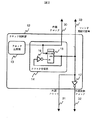
図1には本発明の代表的な実施形態の一つを示している。一つの半導体基板に形成されたマイクロコンピュータ(MPU:マイクロプロセッサユニット)と、一つの半導体基板上に形成されたダブルデータレート方式のシンクロナスDRAM(DDR−SDRAM)21とが示されている。図では、DDR−SDRAMは一つしか示されていないが、一つのマイクロコンピュータに複数のDDR−SDRAMを接続する構成であってもよい。 FIG. 1 shows one typical embodiment of the present invention. A microcomputer (MPU: microprocessor unit) formed on one semiconductor substrate and a double data rate synchronous DRAM (DDR-SDRAM) 21 formed on one semiconductor substrate are shown. Although only one DDR-SDRAM is shown in the figure, a configuration in which a plurality of DDR-SDRAMs are connected to one microcomputer may be employed.
図1のマイクロプロセッサユニット内部の説明を行う。1は21のDDR方式のメモリを制御するメモリインタフェースモジュール、2は中央処理装置(CPU)及びキャッシュメモリ(Cache)とで構成されたモジュール、3はダイレクトメモリアクセスコントローラ(DMAC)モジュールである。2のCPU/Cacheモジュールと3のDMACモジュールは、1のメモリインタフェースモジュールに向けて、メモリに記憶されているデータの読み出し又はメモリにデータを記憶させるため、メモリ内の所定メモリセルを指定するためのアドレスの他に、アクセス要求も出力する。CPU/Cacheモジュールがメモリインタフェースモジュールに対して行うアクセス要求としては、メモリからのリードとメモリへのライトを行うためのメモリアクセス要求と、メモリインタフェースモジュール内部のレジスタ6に対するリード/ライトのレジスタアクセス要求などがある。DMACモジュールがメモリインタフェースモジュールに対して行うアクセス要求としては、メモリのリード/ライトを行うためのメモリアクセス要求がある。
The inside of the microprocessor unit in FIG. 1 will be described.
上記に示した、CPU/Cacheモジュールからメモリインタフェース内のレジスタ6に対するレジスタアクセス要求のうち、レジスタへのライト要求を行う場合、CPU/Cacheモジュールはリクエストとしてレジスタライトアクセス要求をメモリインタフェースモジュール内のリクエスト制御部4に出力する。それと同時に、レジスタ6に書き込むデータを103を介してレジスタ6に出力する。CPU/Cacheモジュールより、レジスタへの書き込みの要求を受けたリクエスト制御部4はレジスタアクセスリクエスト101をレジスタR/W制御部5に出力する。レジスタアクセスリクエストを受けたレジスタR/W制御部は、レジスタ6に対してレジスタ書き込み信号102を出力する。上述した一連の動作により、CPU/Cacheモジュールからレジスタ6に送られるデータがレジスタ6に書き込まれる。
Of the above register access requests from the CPU / Cache module to the
CPU/CacheモジュールがDDR−SDRAMに記憶されているデータを必要とした場合、CPU/Cacheモジュールはリクエストとしてメモリアクセス要求とDDR−SDRAMの所定箇所を指定するためのアドレスをメモリインタフェースモジュール内のリクエスト制御部4に出力する。メモリアクセス要求を受けたリクエスト制御部は、CPU/Cacheモジュールがメモリへのアクセスを要求していることを認識すると、メモリインタフェースモジュール内の外部バス制御部7にメモリアクセスリクエスト104を出力する。メモリアクセスリクエストを受けた外部バス制御部はアドレス制御部8、制御信号生成部9、データ制御部10を制御し、DDR−SDRAMとのメモリアクセスを開始する。
When the CPU / Cache module needs data stored in the DDR-SDRAM, the CPU / Cache module requests a memory access request and an address for designating a predetermined location of the DDR-SDRAM as a request in the memory interface module. Output to the
上述したアドレス制御部8ではあらかじめレジスタに記憶されているデータのうちのメモリアドレスと、リクエスト制御部4から出力されるリクエストアドレス107から、メモリへ出力するアドレス情報を生成する。生成されたアドレスは、DDR−SDRAMに接続されているアドレスバス34を介してメモリ21に転送される。制御信号生成部9では、あらかじめレジスタ6に記憶されたデータのなかのメモリ情報105を外部バス制御部7を介して受け取り、受け取ったメモリ情報にしたがってメモリアクセスに必要なメモリ制御信号35を生成し、メモリに出力する。メモリ制御信号としては、メモリからのリード/メモリへのライト等をメモリに指示するための各種コマンドである。データ制御部10は、外部バス制御部7からの指示により、バスデータバッファ11を制御し、DDR−SDRAMに接続されたデータバス36を介して行われる、マイクロプロセッサとメモリとの間のデータの授受の制御を行う。
The
なお、本実施例ではDMACモジュールを内蔵したマイクロプロセッサを用いているが、DMACモジュールを内蔵していないマイクロプロセッサでもよい。 In this embodiment, a microprocessor with a built-in DMAC module is used, but a microprocessor without a built-in DMAC module may be used.
図2では、図1のマイクロプロセッサの中に形成されているクロック制御部12の詳細例を示す。クロック制御部12は、基準となるクロックを生成するクロック生成部13、クロック生成部13で生成されたクロックの1/2の周波数を生成するクロック分周器14とで主に構成される。クロック生成部13にて生成されたクロックは、本実施例のマイクロプロセッサの基準クロック、つまり、中央処理ユニット等に供給される内部クロック30となる。なお、本実施例では基準クロックはクロック生成部にて生成しているが、外部から供給されるクロックであっても問題ない。
FIG. 2 shows a detailed example of the
クロック分周器14は、ラッチ手段15と分周器用インバータ16とで主に構成される。ラッチ15の出力を分周器用インバータ16を通して反転してラッチの入力とし、クロック信号の立ち上がりでデータを取り込むことで、基準クロックつまり内部クロック13に対して1/2の周波数のクロックが生成される。クロック分周器で生成された内部クロックの1/2の周波数のクロックは、外部クロック31としてマイクロプロセッサの外部、つまり、DDR−SDRAMなどに出力される。また、クロック分周器で生成された内部クロックの1/2の周波数のクロックを外部クロック用インバータ17により反転した信号が、反転クロック32として外部に出力される。更に、基準クロックの1/2の周波数のクロックはメモリインタフェースモジュール1内の外部バス制御部にも送られ、出力コマンド同期化信号33として使用される。クロック分周器などの構成は本実施例の他にも多様な変形例が存在するが、それらについての説明は割愛する。
The
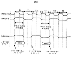
図3にはメモリインタフェースモジュール1でのコマンド同期タイミングを示す。
メモリインタフェースモジュールには、クロック制御部12から出力される、プロセッサの内部クロックと、前記内部クロックの1/2の周波数のコマンド同期化信号33とが供給されている。コマンド同期化信号は、プロセッサ外部のDDR−SDRAMに供給される外部クロックと同じ周波数で、同じ位相をもったクロックである。メモリインタフェースモジュールは、メモリが外部クロック31の立ち上がりで各種コマンドを受け取れるよう制御する。メモリは、外部クロックがLOWの期間(T2)にメモリに対して出力されたコマンドについては、外部クロックの次の立ち上がりの時点で受け取ることが可能であるが、外部クロックがHIGHの期間にメモリに対して与えられたコマンドについては受け取ることが出来ない。そのためコマンド出力可能期間、つまり外部クロックがLOWのときにのみ制御信号を出力し、コマンド出力不可期間には制御信号の出力はしないようにする必要がある。
FIG. 3 shows command synchronization timing in the
The memory interface module is supplied with an internal clock of the processor and a
なお、本実施例では、コマンドの出力サイクルを内部クロック(30)の1サイクルとしているが、コマンド出力サイクルを外部クロック(31)の1サイクルとしてもよい。 In this embodiment, the command output cycle is one cycle of the internal clock (30), but the command output cycle may be one cycle of the external clock (31).
図4にマイクロプロセッサとダブルデータレート(DDR)方式のシンクロナスDRAMとの接続例を示す。DDR−SDRAM21のアクセスに必要なメモリ制御信号にはクロック(CLOCK)、反転クロック(/CLOCK)、クロックイネーブル信号(CKE)、チップセレクト信号(/CS)、ロウアドレスストローブ信号(/RAS)、カラムアドレスストローブ(/CAS)、ライトイネーブル信号(/WE)、データマスクイネーブル信号(DQM)、およびデータストローブ信号(DQS)がある。これらのメモリ制御信号の他には、メモリのアドレスを指定するためのアドレス(Addr.)と、マイクロプロセッサとメモリとの間でやり取りされるデータ(DATA)とがある。マイクロプロセッサは各種制御信号を出力することでダブルデータレートシンクロナスDRAMに対して、メモリの動作を規定するための各種コマンドやアドレス、データを与え、メモリからのリードやメモリへのライトアクセスを実現する。尚、図面において、アルファベットの上部に横線が入っている信号、及び、上記においてアルファベットの前に斜線が入っている信号は、信号がLOWレベルになったときに信号が活性化することを示している。
FIG. 4 shows an example of connection between a microprocessor and a double data rate (DDR) synchronous DRAM. Memory control signals necessary for accessing the DDR-
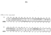
図5にはマイクロプロセッサ内のレジスタ6の概要図を示す。特に制限されないが、本実施形態ではレジスタ6は32ビットのレジスタで構成される。TRC0から2、 TPC0から2、RCD0から1、TRWL2から0にはメモリアクセスのタイミング情報が設定される。また、AMX2から0にはロウアドレスとカラムアドレスのそれぞれのビット数が設定される。これらのレジスタ6の内容は、使用するDDR−SDRAMの種類、動作周波数に合わせて設定することが可能である。
FIG. 5 shows a schematic diagram of the
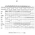
図6には、マイクロプロセッサによるDDR−SDRAMからのリードアクセス時のタイミングチャート、図7には、マイクロプロセッサにからDDR−SDRAMへのライトアクセス時のタイミングチャートを示している。 FIG. 6 shows a timing chart at the time of read access from the DDR-SDRAM by the microprocessor, and FIG. 7 shows a timing chart at the time of write access from the microprocessor to the DDR-SDRAM.
図6において、プロセッサの内部クロックの1周期であるTrサイクルでDDR−SDARMに対して図示していないACTVコマンドを発行する。それと伴にロウアドレス(Row)をアドレス(Addr.)線を介してメモりに通知する。Trに続くTrwサイクルの立ち上がり、つまり外部クロックの立ち上がりでメモリはアドレス線を介して印加されているロウアドレス(Row)を取り込む。その後メモリ21は規定のサイクルだけ待機する。規定サイクル経過した後、Tc1サイクルでREADコマンドを発行してカラムアドレス(c1)を通知し、Tc2サイクルの開始時、つまり外部クロックの立ち上がりの際にメモリ21はアドレス線を介して印加されているカラムアドレス(c1)を取り込む。その後、メモリに事前に規定されているレイテンシに応じた周期、Tc2、Tc3を待ってからリードDATAのサンプリングを行なう。なお、本実施例ではメモリのバースト長を4としているためTc1サイクルでREADコマンドを発行した4サイクル後に、後続のコマンドとしてオートプリチャージつきリードコマンドであるREADAコマンドを発行し、プリチャージを実行している。
In FIG. 6, an ACTV command (not shown) is issued to DDR-SDARM in a Tr cycle that is one cycle of the internal clock of the processor. At the same time, the row address (Row) is notified to the memory via the address (Addr.) Line. At the rise of the Trw cycle following Tr, that is, at the rise of the external clock, the memory takes in the row address (Row) applied through the address line. Thereafter, the
メモリへの書き込みの際のタイミングを示している図7についても、TrサイクルでACTVコマンドを発行し、アドレス線(Addr.)を介してメモリに対してロウアドレスを供給する。メモリへ供給される外部クロックの、Trに続く次のサイクルであるTrwの立ち上がりで、メモリは供給されたロウアドレスを取り込む。次に、Tw1サイクルでWRITコマンドを発行し、アドレス線を介してメモリにカラムアドレスを供給する。更にTw1のサイクルにおいて、ライトDATAのドライブを行なう。なお、本実施例ではメモリのバースト長を4としているためTw1サイクルでWRITコマンドを発行した4サイクル後に、後続のコマンドとしてオートプリチャージつきライトコマンドであるWRITAコマンドを発行し、プリチャージを実行している。 Also in FIG. 7 showing the timing at the time of writing to the memory, the ACTV command is issued in the Tr cycle, and the row address is supplied to the memory via the address line (Addr.). At the rising edge of Trw, which is the next cycle following Tr, of the external clock supplied to the memory, the memory takes in the supplied row address. Next, a WRIT command is issued in the Tw1 cycle, and a column address is supplied to the memory via the address line. Further, in the cycle of Tw1, write DATA is driven. In this embodiment, since the memory burst length is 4, after 4 cycles of issuing the WRIT command in the Tw1 cycle, a WRITE command, which is a write command with auto precharge, is issued as a subsequent command, and the precharge is executed. ing.
さらに続くアクセスがTrで発行した時のロウアドレスと同一アドレスに対するアクセスの場合、アクセスの終了時にプリチャージつきのリード/ライトコマンドではなく、プリチャージなしのリード/ライトコマンドで終了し、Tc1サイクルのリードもしくはライトコマンドを発行するだけでアクセスを続けることも可能であり、Tr、Trwサイクルだけ高速にアクセスを行なうことができる。 If the subsequent access is to the same address as the row address issued by Tr, the read / write command without precharge is terminated at the end of the access, not the read / write command with precharge, and the read of the Tc1 cycle is performed. Alternatively, access can be continued only by issuing a write command, and access can be performed at high speed for Tr and Trw cycles.
図8には、図1で示したバスデータバッファ11と制御信号生成部9との詳細を示している。制御信号生成部については、データストローブ制御部50のみを示している。DDR−SDRAMでは、データ読み出し時にメモリから出力されるデータ信号の変化と、データストローブ信号の変化とは同一のタイミングである。メモリインタフェースは、データストローブ信号を外部クロックに対して90度位相を遅らせた信号でデータを取り込むようになっている。また、メモリ動作クロックとデータ変化タイミングは規定が無く、メモリ動作クロックでデータをサンプリングすることはできない。
FIG. 8 shows details of the
一方、データ書き込み時、メモリはデータをデータストローブ信号の立ち上がりエッジ、及び立ち下がりエッジで取り込めるようにデータストローブ信号の出力が規定され、データストローブ信号に対してデータのセットアップ/ホールド時間が規定されている。 On the other hand, when writing data, the output of the data strobe signal is specified so that the memory can capture data at the rising edge and falling edge of the data strobe signal, and the data setup / hold time is specified for the data strobe signal. Yes.
データの書き込み時に、メモリコントローラは外部クロックの立ち上がりと立ち下がりに同期してデータを出力し、同時に外部クロックに対して90度位相の遅れたデータストローブ信号を出力する必要がある。
メモリ動作の基準となる外部クロックと、外部クロックの2倍の周波数の内部クロックを共にプロセッサ内部で生成するため、外部クロックと内部クロックの位相差の制御が可能となる。また、外部クロックの2倍の周波数の内部クロックを使用することで、外部クロックに対して90度の位相シフトを容易に行うことが出来る。
At the time of writing data, the memory controller needs to output data in synchronization with the rising and falling edges of the external clock, and simultaneously output a data strobe signal that is delayed by 90 degrees from the external clock.
Since both the external clock serving as a reference for memory operation and an internal clock having a frequency twice that of the external clock are generated inside the processor, the phase difference between the external clock and the internal clock can be controlled. Further, by using an internal clock having a frequency twice that of the external clock, it is possible to easily perform a phase shift of 90 degrees with respect to the external clock.
外部クロックと内部クロックの位相差の制御が可能であるため、データの読み出し時のデータの取り込みの際にデータストローブ信号を使用せず、内部クロックの立ち上がりでデータを取り込むことが可能となる。内部クロックは外部クロックの2倍の周波数であり、外部クロックの立ち上がりと立ち下がりに同期して変化するデータを内部クロックの立ち上がりで取り込むことが可能となる。メモリの出力するデータストローブ信号を使用した場合、位相を90度遅らせるための位相シフト回路が必要となるが、本実施例の場合は特に必要とはならない。このことにより、周波数の変更に伴っても、位相シフト回路の変更が不要となるといった利点もある。更に、プロセッサ外部にメモリコントローラを設けた場合、データストローブ信号を90度位相を遅らせて取り込まれたデータとプロセッサ動作の基準となるクロックとの間に相関関係が無く、非同期信号となるためデータ信号の同期化回路が必要となってしまう。つまり速度的に不利となる。 Since the phase difference between the external clock and the internal clock can be controlled, it is possible to capture data at the rising edge of the internal clock without using a data strobe signal when capturing data when reading data. The internal clock has twice the frequency of the external clock, and data that changes in synchronization with the rise and fall of the external clock can be captured at the rise of the internal clock. When the data strobe signal output from the memory is used, a phase shift circuit for delaying the phase by 90 degrees is required. However, this embodiment is not particularly necessary. As a result, there is an advantage that even if the frequency is changed, it is not necessary to change the phase shift circuit. Further, when a memory controller is provided outside the processor, there is no correlation between the data taken by delaying the phase of the data strobe signal by 90 degrees and the reference clock for the processor operation, and the data signal becomes an asynchronous signal. Synchronization circuit becomes necessary. In other words, it is disadvantageous in terms of speed.
データの書き込み時には、内部クロックを使用し、内部クロックの立ち下がりでデータストローブ信号が変化するように出力することで、外部クロックの90度位相シフトが容易に可能となる。読み出し時と同様に位相シフト回路が不要となる。データ信号はデータの読み込み時にはメモリ側からドライブされるので信号が衝突しないようにトライステートバッファによりドライブコントロールを行う。 When writing data, the internal clock is used and output so that the data strobe signal changes at the falling edge of the internal clock, whereby the 90-degree phase shift of the external clock can be easily performed. A phase shift circuit is not required as in the case of reading. Since the data signal is driven from the memory side when data is read, drive control is performed by a tri-state buffer so that the signal does not collide.
また、外部クロックの2倍の周波数の内部クロックを使用することで、速度性能の向上のための外部クロックの周波数の変更にも対応できる。 Further, by using an internal clock having a frequency twice that of the external clock, it is possible to cope with a change in the frequency of the external clock for improving speed performance.
以上、プロセッサ内部にDDR−SDRAMのメモリコントローラ及びクロック制御部を内蔵することによって、プロセッサ動作の基準となる内部クロックとメモリ動作の基準となる外部クロックとの供給が可能となり、メモリ制御信号の生成やデータ信号の入出力制御が簡単な回路で実現できる。更に、不要な同期化回路の削減も可能となる。 As described above, by incorporating the DDR-SDRAM memory controller and the clock control unit in the processor, it is possible to supply the internal clock as the reference for the processor operation and the external clock as the reference for the memory operation, and generate the memory control signal. And data signal input / output control can be realized with a simple circuit. Further, unnecessary synchronization circuits can be reduced.
尚、上述した実施形態はあくまでも本発明の一つの実施形態であり、本発明が上記実施形態に限定されるものではない。例えば、図3に示した内部クロック、同期化信号及び外部クロックについての位相は図面に限定されるものではなく、同期化信号及び/又は外部クロックは、図面と反転した信号であってもよい。また、図8に関連する記載において、メモリからのデータの読み出しの際、内部クロックの立ち上がりでデータを取り込むのではなく、クロックの立ち下がりでデータを取り込むことも可能である。同様にデータの書き込みの際のタイミングについても同様のことが言える。 In addition, embodiment mentioned above is one embodiment of this invention to the last, and this invention is not limited to the said embodiment. For example, the phases of the internal clock, the synchronization signal, and the external clock shown in FIG. 3 are not limited to those in the drawing, and the synchronization signal and / or the external clock may be a signal inverted from the drawing. In the description related to FIG. 8, when reading data from the memory, it is possible to capture data at the falling edge of the clock instead of capturing data at the rising edge of the internal clock. Similarly, the same can be said for the timing of data writing.
1 メモリインタフェースモジュール
2 CPU/Cacheモジュール
3 DMAC
4 リクエスト制御部
5 レジスタR/W制御部
6 レジスタ
7 外部バス制御部
8 アドレス制御部
9 制御信号
10 データ制御部
11 データバッファ
12 クロック制御部
13 クロック生成部
14 クロック分周器
15 ラッチ
16 分周器用インバータ
17 外部クロック用インバータ
20 マイクロプロセッサ
21 ダブルデータレートシンクロナスDRAM(DDR−SDRAM)
30 内部クロック
31 外部クロック
32 反転クロック
33 出力コマンド同期化信号
34 アドレス
35 メモリ制御信号
36 データ
101 レジスタアクセスリクエスト
102 レジスタ書き込み信号
103 データ
104 メモリアクセスリクエスト
105 メモリタイミング情報
106 メモリアドレス情報
107 リクエストアドレス
1
4
30
Claims (1)
前記中央処理ユニットに接続されたメモリ制御手段と、
前記中央処理ユニットと前記メモリ制御手段とにクロックを供給するためのクロック制御部と、を有し、一つの半導体チップ上に形成されたマイクロコンピュータであって、
前記マイクロコンピュータは、前記クロック制御部から供給されたクロックを外部クロックとしてマイクロコンピュータの外部に出力し、前記外部クロックを反転した外部反転クロックをマイクロコンピュータの外部に出力し、
前記メモリ制御手段は、前記クロックに対応し、第1の電位状態と第2の電位状態とに遷移するデータストローブ信号を生成可能であり、
前記メモリ制御手段によって制御されるメモリは、前記データストローブ信号の立ち上がりエッジと立ち下がりエッジに同期してデータの入出力を行うことが可能なダブルデータレート方式の同期型メモリであり、
前記メモリ制御手段は、前記同期型メモリにデータを書き込むとき、前記データストローブ信号の立ち上がりエッジと立ち下がりエッジに同期してデータを外部に出力し、
前記中央処理ユニットは、前記同期型メモリにアクセスするためのメモリアドレスを生成し、
前記メモリ制御手段は、前記外部クロックに同期して前記メモリアドレスを出力することが可能であることを特徴とするマイクロコンピュータ。 A central processing unit;
Memory control means connected to the central processing unit;
A clock controller for supplying a clock to the central processing unit and the memory control means, and a microcomputer formed on one semiconductor chip,
The microcomputer outputs the clock supplied from the clock control unit as an external clock to the outside of the microcomputer, and outputs an external inverted clock obtained by inverting the external clock to the outside of the microcomputer.
The memory control means can generate a data strobe signal corresponding to the clock and transitioning between a first potential state and a second potential state;
The memory controlled by the memory control means is a double data rate synchronous memory capable of inputting / outputting data in synchronization with a rising edge and a falling edge of the data strobe signal,
The memory control means outputs data to the outside in synchronization with the rising edge and falling edge of the data strobe signal when writing data to the synchronous memory,
The central processing unit generates a memory address for accessing the synchronous memory;
The microcomputer characterized in that the memory control means can output the memory address in synchronization with the external clock.
Priority Applications (1)
| Application Number | Priority Date | Filing Date | Title |
|---|---|---|---|
| JP2009245314A JP4785153B2 (en) | 2009-10-26 | 2009-10-26 | Microcomputer and microcomputer system |
Applications Claiming Priority (1)
| Application Number | Priority Date | Filing Date | Title |
|---|---|---|---|
| JP2009245314A JP4785153B2 (en) | 2009-10-26 | 2009-10-26 | Microcomputer and microcomputer system |
Related Parent Applications (1)
| Application Number | Title | Priority Date | Filing Date |
|---|---|---|---|
| JP2006155841A Division JP2006244528A (en) | 2006-06-05 | 2006-06-05 | Microcomputer |
Related Child Applications (1)
| Application Number | Title | Priority Date | Filing Date |
|---|---|---|---|
| JP2011048604A Division JP2011118932A (en) | 2011-03-07 | 2011-03-07 | Microcomputer |
Publications (2)
| Publication Number | Publication Date |
|---|---|
| JP2010020801A true JP2010020801A (en) | 2010-01-28 |
| JP4785153B2 JP4785153B2 (en) | 2011-10-05 |
Family
ID=41705546
Family Applications (1)
| Application Number | Title | Priority Date | Filing Date |
|---|---|---|---|
| JP2009245314A Expired - Fee Related JP4785153B2 (en) | 2009-10-26 | 2009-10-26 | Microcomputer and microcomputer system |
Country Status (1)
| Country | Link |
|---|---|
| JP (1) | JP4785153B2 (en) |
Cited By (1)
| Publication number | Priority date | Publication date | Assignee | Title |
|---|---|---|---|---|
| KR101113188B1 (en) | 2010-09-30 | 2012-02-16 | 주식회사 하이닉스반도체 | Operation speed changeable nonvolatile memory apparatus and control method of complementary signal therefor |
Citations (7)
| Publication number | Priority date | Publication date | Assignee | Title |
|---|---|---|---|---|
| JPH05120114A (en) * | 1991-04-23 | 1993-05-18 | Texas Instr Inc <Ti> | Random access memory which is operated in synchronization with microprocessor |
| JPH07105173A (en) * | 1993-09-30 | 1995-04-21 | Hitachi Ltd | Data processor |
| JPH07160249A (en) * | 1993-10-15 | 1995-06-23 | Hitachi Ltd | Data processor and data processing system |
| JPH07282000A (en) * | 1994-04-04 | 1995-10-27 | Hitachi Ltd | Bus interface circuit and data transfer system |
| JPH09106671A (en) * | 1995-09-11 | 1997-04-22 | Samsung Electron Co Ltd | Semiconductor memory device and its read/write method |
| JPH10199239A (en) * | 1996-12-27 | 1998-07-31 | Fujitsu Ltd | Semiconductor memory device system and semiconductor memory device |
| JPH11505047A (en) * | 1995-05-05 | 1999-05-11 | シリコン、グラフィクス、インコーポレイテッド | Source synchronous clock type data link |
-
2009
- 2009-10-26 JP JP2009245314A patent/JP4785153B2/en not_active Expired - Fee Related
Patent Citations (7)
| Publication number | Priority date | Publication date | Assignee | Title |
|---|---|---|---|---|
| JPH05120114A (en) * | 1991-04-23 | 1993-05-18 | Texas Instr Inc <Ti> | Random access memory which is operated in synchronization with microprocessor |
| JPH07105173A (en) * | 1993-09-30 | 1995-04-21 | Hitachi Ltd | Data processor |
| JPH07160249A (en) * | 1993-10-15 | 1995-06-23 | Hitachi Ltd | Data processor and data processing system |
| JPH07282000A (en) * | 1994-04-04 | 1995-10-27 | Hitachi Ltd | Bus interface circuit and data transfer system |
| JPH11505047A (en) * | 1995-05-05 | 1999-05-11 | シリコン、グラフィクス、インコーポレイテッド | Source synchronous clock type data link |
| JPH09106671A (en) * | 1995-09-11 | 1997-04-22 | Samsung Electron Co Ltd | Semiconductor memory device and its read/write method |
| JPH10199239A (en) * | 1996-12-27 | 1998-07-31 | Fujitsu Ltd | Semiconductor memory device system and semiconductor memory device |
Cited By (2)
| Publication number | Priority date | Publication date | Assignee | Title |
|---|---|---|---|---|
| KR101113188B1 (en) | 2010-09-30 | 2012-02-16 | 주식회사 하이닉스반도체 | Operation speed changeable nonvolatile memory apparatus and control method of complementary signal therefor |
| US8482996B2 (en) | 2010-09-30 | 2013-07-09 | SK Hynix Inc. | Nonvolatile memory apparatus with changeable operation speed and related signal control method |
Also Published As
| Publication number | Publication date |
|---|---|
| JP4785153B2 (en) | 2011-10-05 |
Similar Documents
| Publication | Publication Date | Title |
|---|---|---|
| JP2002007200A (en) | Memory controller and operation switching method and interface device and semiconductor integrated chip and recording medium | |
| US7212465B2 (en) | Clock signal generation apparatus for use in semiconductor memory device and its method | |
| JP4723679B2 (en) | Semiconductor memory device, memory system, and refresh control method for semiconductor memory device | |
| US7716443B2 (en) | Apparatus and method for controlling memory interface | |
| JP2002358231A (en) | Memory control system | |
| JPH1116349A (en) | Synchronous semiconductor memory device | |
| JP3272914B2 (en) | Synchronous semiconductor device | |
| JP2010165422A (en) | Semiconductor storage device and read latency adjustment method therefor, memory system, and semiconductor device | |
| US20080052481A1 (en) | Method and circuit for transmitting a memory clock signal | |
| JP5733126B2 (en) | Memory interface circuit and timing adjustment method | |
| JP2000030456A (en) | Memory device | |
| JP2002074952A (en) | Synchronous type semiconductor memory, and control method of its input circuit | |
| JP2002304885A (en) | Semiconductor integrated circuit | |
| JPH09180438A (en) | Memory control device | |
| JP2011118932A (en) | Microcomputer | |
| JP3865972B2 (en) | Microcomputer and system using microcomputer | |
| JP2000268565A (en) | Synchronous type semiconductor storage device | |
| JP4785153B2 (en) | Microcomputer and microcomputer system | |
| JP2003173290A (en) | Memory controller | |
| JP2009282721A (en) | Memory controller, memory control system, and method of controlling amount of delay in memory | |
| US7492661B2 (en) | Command generating circuit and semiconductor memory device having the same | |
| JP2000231788A (en) | Semiconductor memory | |
| JP2008192264A (en) | Semiconductor memory device | |
| JP2006244528A (en) | Microcomputer | |
| US7103707B2 (en) | Access control unit and method for use with synchronous dynamic random access memory device |
Legal Events
| Date | Code | Title | Description |
|---|---|---|---|
| A621 | Written request for application examination |
Free format text: JAPANESE INTERMEDIATE CODE: A621 Effective date: 20091125 |
|
| A711 | Notification of change in applicant |
Free format text: JAPANESE INTERMEDIATE CODE: A712 Effective date: 20100527 |
|
| A977 | Report on retrieval |
Free format text: JAPANESE INTERMEDIATE CODE: A971007 Effective date: 20101220 |
|
| A131 | Notification of reasons for refusal |
Free format text: JAPANESE INTERMEDIATE CODE: A131 Effective date: 20110105 |
|
| A521 | Written amendment |
Free format text: JAPANESE INTERMEDIATE CODE: A523 Effective date: 20110307 |
|
| A131 | Notification of reasons for refusal |
Free format text: JAPANESE INTERMEDIATE CODE: A131 Effective date: 20110421 |
|
| A521 | Written amendment |
Free format text: JAPANESE INTERMEDIATE CODE: A523 Effective date: 20110615 |
|
| TRDD | Decision of grant or rejection written | ||
| A01 | Written decision to grant a patent or to grant a registration (utility model) |
Free format text: JAPANESE INTERMEDIATE CODE: A01 Effective date: 20110707 |
|
| A01 | Written decision to grant a patent or to grant a registration (utility model) |
Free format text: JAPANESE INTERMEDIATE CODE: A01 |
|
| A61 | First payment of annual fees (during grant procedure) |
Free format text: JAPANESE INTERMEDIATE CODE: A61 Effective date: 20110708 |
|
| R150 | Certificate of patent or registration of utility model |
Free format text: JAPANESE INTERMEDIATE CODE: R150 |
|
| FPAY | Renewal fee payment (event date is renewal date of database) |
Free format text: PAYMENT UNTIL: 20140722 Year of fee payment: 3 |
|
| S531 | Written request for registration of change of domicile |
Free format text: JAPANESE INTERMEDIATE CODE: R313531 |
|
| R350 | Written notification of registration of transfer |
Free format text: JAPANESE INTERMEDIATE CODE: R350 |
|
| LAPS | Cancellation because of no payment of annual fees |