JP2010020387A - Memory access control apparatus and image pickup apparatus - Google Patents
Memory access control apparatus and image pickup apparatus Download PDFInfo
- Publication number
- JP2010020387A JP2010020387A JP2008177846A JP2008177846A JP2010020387A JP 2010020387 A JP2010020387 A JP 2010020387A JP 2008177846 A JP2008177846 A JP 2008177846A JP 2008177846 A JP2008177846 A JP 2008177846A JP 2010020387 A JP2010020387 A JP 2010020387A
- Authority
- JP
- Japan
- Prior art keywords
- memory
- signal
- ddr
- phy
- request signal
- Prior art date
- Legal status (The legal status is an assumption and is not a legal conclusion. Google has not performed a legal analysis and makes no representation as to the accuracy of the status listed.)
- Granted
Links
Images


Classifications
-
- G—PHYSICS
- G06—COMPUTING; CALCULATING OR COUNTING
- G06F—ELECTRIC DIGITAL DATA PROCESSING
- G06F13/00—Interconnection of, or transfer of information or other signals between, memories, input/output devices or central processing units
- G06F13/14—Handling requests for interconnection or transfer
- G06F13/16—Handling requests for interconnection or transfer for access to memory bus
- G06F13/1668—Details of memory controller
- G06F13/1689—Synchronisation and timing concerns
-
- H—ELECTRICITY
- H04—ELECTRIC COMMUNICATION TECHNIQUE
- H04N—PICTORIAL COMMUNICATION, e.g. TELEVISION
- H04N23/00—Cameras or camera modules comprising electronic image sensors; Control thereof
- H04N23/60—Control of cameras or camera modules
- H04N23/665—Control of cameras or camera modules involving internal camera communication with the image sensor, e.g. synchronising or multiplexing SSIS control signals
-
- H—ELECTRICITY
- H04—ELECTRIC COMMUNICATION TECHNIQUE
- H04N—PICTORIAL COMMUNICATION, e.g. TELEVISION
- H04N23/00—Cameras or camera modules comprising electronic image sensors; Control thereof
- H04N23/60—Control of cameras or camera modules
- H04N23/667—Camera operation mode switching, e.g. between still and video, sport and normal or high- and low-resolution modes
Landscapes
- Engineering & Computer Science (AREA)
- Multimedia (AREA)
- Signal Processing (AREA)
- Theoretical Computer Science (AREA)
- Physics & Mathematics (AREA)
- General Engineering & Computer Science (AREA)
- General Physics & Mathematics (AREA)
- Memory System (AREA)
- Dram (AREA)
Abstract
Description
本発明は、メモリアクセス制御装置および撮像装置に関し、特に、高速でデータ転送を行うメモリを搭載する機器において、周波数変更の処理に伴う影響を極めて小さくすることができるようにするメモリアクセス制御装置および撮像装置に関する。 The present invention relates to a memory access control device and an imaging device, and more particularly to a memory access control device and a memory access control device that can extremely reduce the influence of frequency change processing in a device equipped with a memory that performs data transfer at high speed. The present invention relates to an imaging apparatus.
近年、例えば、CPUとメインメモリ間のデータ転送の高速化のため、コンピュータ内の各回路間で同期を取る際に、クロック信号の立上がり時と立下がり時の両方を利用し、片方のみを利用する場合に比べ単位時間あたりの処理効率を2倍に高めることができるDDR(Double Data Rate)方式が多く採用されている。さらに、DDRを高性能化し、省電力化を図った規格DDR2も提唱されている。 In recent years, for example, in order to speed up data transfer between the CPU and main memory, when synchronizing each circuit in the computer, both the rising and falling edges of the clock signal are used, and only one of them is used. Compared to the case, the DDR (Double Data Rate) method, which can double the processing efficiency per unit time, is adopted. In addition, DDR2 has been proposed to improve the performance of DDR and save power.
DDR SDRAM、DDR2 SDRAM、LPDDR(Low Power Double Data Rate)SDRAMなどを搭載するシステムにおいては、消費電力を抑制するために、例えば、必要なメモリ容量、システムの動作モードなどに応じて、クロック周波数を変更する制御が行われることが一般的である。高速のクロックでシステムを動作させると、当然単位時間あたりの消費電力量が増えるからである。 In systems equipped with DDR SDRAM, DDR2 SDRAM, LPDDR (Low Power Double Data Rate) SDRAM, etc., to reduce power consumption, for example, the clock frequency is set according to the required memory capacity, system operation mode, etc. In general, control to change is performed. This is because operating the system with a high-speed clock naturally increases the amount of power consumed per unit time.
DDR、DDR2、LPDDRSDRAMなどを搭載するシステムにおいては、外部から供給されるクロック信号に同期して内部回路を動作させているが、チップ上の回路レイアウトに依存する信号線の配線長によりスキューが発生し、基準となるクロックに対するデータ・ストローブ信号DQSの位相誤差となって現れる。このため、高速な動作クロックで動作するDDRSDRAMからデータの読出しを行なう際には、位相調整を極めて厳格に行なう必要がある。位相調整のため、例えば、DLL(Delay Locked Loop)と称される、配線負荷などにより発生する外部インタフェースの遅延時間を制御し、内部クロックとの同期を調整する回路などが搭載される。また、位相調整のため、DL(Delay Line)が用いられる場合もある。 In a system equipped with DDR, DDR2, LPDDRSDRAM, etc., the internal circuit is operated in synchronization with an externally supplied clock signal. However, skew occurs due to the wiring length of the signal line depending on the circuit layout on the chip. However, it appears as a phase error of the data strobe signal DQS with respect to the reference clock. For this reason, when data is read from DDRSDRAM that operates at a high-speed operation clock, it is necessary to perform phase adjustment very strictly. For phase adjustment, for example, a circuit called DLL (Delay Locked Loop) that controls the delay time of an external interface generated by a wiring load or the like and adjusts synchronization with an internal clock is mounted. Further, DL (Delay Line) may be used for phase adjustment.
DDR、DDR2、LPDDRSDRAMなどを搭載するシステムにおけるクロック周波数を変更するものとして、例えば、メモリコントローラで使用する周波数に応じて、DLL(Delay Locked Loop)とDL(Delay Line)を搭載して、使い分けることが可能なシステムが提案されている(例えば、特許文献1参照)。 In order to change the clock frequency in a system equipped with DDR, DDR2, LPDDRSDRAM, etc., for example, depending on the frequency used in the memory controller, DLL (Delay Locked Loop) and DL (Delay Line) are installed and used properly Has been proposed (see, for example, Patent Document 1).
また、動画撮影の開始が指示される以前は、制御部のクロック周波数を通常の周波数とし、モニタリング状態における無駄な電力消費を無くすことにより、電池寿命の長期化を図り、動画撮影の開始が指示されたら、その時点で、クロック切り替え制御部によってクロック周波数を大幅に上げ、MPEG変換部が動画データのエンコード処理に際してリファレンスデータやサーチデータなどを記憶するSDRAMのアクセス速度を上げることにより、リアルタイムでの動画圧縮を可能とするシステムも提案されている(例えば、特許文献2参照)。 In addition, before the start of moving image shooting is instructed, the clock frequency of the control unit is set to the normal frequency, eliminating unnecessary power consumption in the monitoring state, thereby extending the battery life and instructing the start of moving image shooting. At that time, the clock switching control unit significantly increases the clock frequency, and the MPEG conversion unit increases the access speed of the SDRAM that stores reference data, search data, etc. during the encoding process of the moving image data. A system that enables moving image compression has also been proposed (see, for example, Patent Document 2).
しかしながら、特許文献1、特許文献2の技術では、周波数変更を行うための制御プログラムが複雑になる。
However, in the techniques of Patent Document 1 and
また、周波数変更を行うための制御プログラムを実行するために、命令コードやワークメモリが必要になり、周波数変更を行う処理を実行する際にメモリにアクセスできなくなることがあるため、それらの命令コードをメモリ以外のROMやSRAMなどに保持しておく必要がある。 In addition, instruction code and work memory are required to execute the control program for changing the frequency, and the memory may become inaccessible when executing the process for changing the frequency. Must be stored in a ROM or SRAM other than memory.
さらに、周波数変更の処理に要する時間が長くなるため、その間のメモリへのアクセスの制限に伴う影響が大きくなる。 Furthermore, since the time required for the frequency change process becomes long, the influence due to the restriction of access to the memory during that time increases.
本発明はこのような状況に鑑みてなされたものであり、高速でデータ転送を行うメモリを搭載する機器において、周波数変更の処理に伴う影響を極めて小さくすることができるようにするものである。 The present invention has been made in view of such a situation, and is intended to make it possible to extremely reduce the influence associated with frequency change processing in a device equipped with a memory that performs high-speed data transfer.
本発明の第1の側面は、マスタデバイスによるDDR(Double Data Rate)方式を採用したメモリに対するアクセスの有無を表すブランキング信号に基づいて、前記メモリを制御するメモリコントローラに、前記メモリのセルフリフレッシュモードでの稼動を制御させる要求信号を出力し、前記メモリコントローラから供給される前記要求信号に対する応答信号に基づいて、前記メモリコントローラと前記メモリとの間のインタフェース信号のタイミング調整を行うDDR-PHYのリセットの要求信号を、前記DDR-PHYを制御するDDR-PHY制御部に出力し、前記DDR-PHY制御部から供給される前記要求信号に対する応答信号に基づいて、クロック信号の周波数を制御するクロック制御部に、クロック周波数の切り替えの要求信号を出力し、前記クロック制御部から供給される前記要求信号に対する応答信号に基づいて、切り換え後のクロック周波数に応じた前記DDR-PHYのパラメータの設定の要求信号を、DDR-PHY制御部に出力し、前記DDR-PHY制御部から供給される前記要求信号に対する応答信号に基づいて、前記メモリのセルフリフレッシュモードでの稼動の解除制御させる要求信号を、前記メモリコントローラに出力することで、前記DDR方式を採用したメモリのクロック周波数を変更するメモリアクセス制御装置である。 According to a first aspect of the present invention, there is provided a memory controller for controlling the memory based on a blanking signal indicating the presence / absence of access to a memory adopting a DDR (Double Data Rate) method by a master device. DDR-PHY that outputs a request signal for controlling operation in a mode and adjusts the timing of an interface signal between the memory controller and the memory based on a response signal to the request signal supplied from the memory controller The reset request signal is output to the DDR-PHY control unit that controls the DDR-PHY, and the frequency of the clock signal is controlled based on the response signal to the request signal supplied from the DDR-PHY control unit. A clock frequency switching request signal is output to the clock control unit and supplied from the clock control unit. Based on the response signal to the request signal, the DDR-PHY parameter setting request signal corresponding to the clock frequency after switching is output to the DDR-PHY control unit and supplied from the DDR-PHY control unit. Based on the response signal to the request signal, the memory controller adopting the DDR method changes the clock frequency of the memory by outputting a request signal for controlling the release of the operation of the memory in the self-refresh mode to the memory controller. A memory access control device.
複数の前記マスタデバイスを有する電子機器に搭載され、前記電子機器の中央処理装置から周波数変更の要求信号が出力された場合、前記DDR方式を採用したメモリのクロック周波数の変更を行い、前記周波数の変更が完了したとき、前記周波数の変更の完了を通知する信号を、前記中央処理装置に出力するようにすることができる。 When the frequency change request signal is output from the central processing unit of the electronic device, mounted on the electronic device having a plurality of the master devices, the clock frequency of the memory adopting the DDR method is changed, and the frequency When the change is completed, a signal notifying the completion of the frequency change can be output to the central processing unit.
複数の前記マスタデバイスのうち、処理の遅延の発生による影響が大きいリアルタイム系マスタデバイスが、前記DDR方式を採用したメモリにアクセスしていない時間を、ブランキング信号に基づいて特定し、前記DDR方式を採用したメモリのクロック周波数の変更を行うようにすることができる。 Among the plurality of master devices, a real-time master device that is greatly influenced by the occurrence of processing delay specifies a time during which the memory adopting the DDR method is not accessed based on a blanking signal, and the DDR method It is possible to change the clock frequency of the memory employing the above.
本発明の第1の側面においては、マスタデバイスによるDDR(Double Data Rate)方式を採用したメモリに対するアクセスの有無を表すブランキング信号に基づいて、前記メモリを制御するメモリコントローラに、前記メモリのセルフリフレッシュモードでの稼動を制御させる要求信号が出力され、前記メモリコントローラから供給される前記要求信号に対する応答信号に基づいて、前記メモリコントローラと前記メモリとの間のインタフェース信号のタイミング調整を行うDDR-PHYのリセットの要求信号が、前記DDR-PHYを制御するDDR-PHY制御部に出力され、前記DDR-PHY制御部から供給される前記要求信号に対する応答信号に基づいて、クロック信号の周波数を制御するクロック制御部に、クロック周波数の切り替えの要求信号が出力され、前記クロック制御部から供給される前記要求信号に対する応答信号に基づいて、切り換え後のクロック周波数に応じた前記DDR-PHYのパラメータの設定の要求信号が、DDR-PHY制御部に出力され、前記DDR-PHY制御部から供給される前記要求信号に対する応答信号に基づいて、前記メモリのセルフリフレッシュモードでの稼動の解除制御させる要求信号が、前記メモリコントローラに出力されることで、前記DDR方式を採用したメモリのクロック周波数が変更される。 In the first aspect of the present invention, the memory controller that controls the memory based on a blanking signal indicating the presence or absence of access to the memory adopting the DDR (Double Data Rate) method by the master device is provided with the self-memory of the memory. A request signal for controlling operation in the refresh mode is output, and DDR- adjusts the timing of an interface signal between the memory controller and the memory based on a response signal to the request signal supplied from the memory controller. A PHY reset request signal is output to the DDR-PHY control unit that controls the DDR-PHY, and the frequency of the clock signal is controlled based on the response signal to the request signal supplied from the DDR-PHY control unit. A clock frequency switching request signal is output to the clock control unit, and the clock control unit Based on the response signal to the request signal supplied from the control unit, a request signal for setting the DDR-PHY parameters according to the clock frequency after switching is output to the DDR-PHY control unit, and the DDR-PHY control Based on a response signal to the request signal supplied from the memory unit, a request signal for controlling the release of the operation in the self-refresh mode of the memory is output to the memory controller. The clock frequency is changed.
本発明の第2の側面は、画像を撮像する撮像手段と、前記撮像された画像の表示に関する処理を行うマスタデバイスと、前記マスタデバイスが処理するデータを記憶するDDR(Double Data Rate)方式を採用したメモリと、中央処理装置からの指令に基づいて前記DDR方式を採用したメモリの周波数を変更するメモリアクセス制御装置とを備え、前記メモリアクセス制御装置は、前記マスタデバイスによる前記メモリに対するアクセスの有無を表すブランキング信号に基づいて、前記メモリを制御するメモリコントローラに、前記メモリのセルフリフレッシュモードでの稼動を制御させる要求信号を出力し、前記メモリコントローラから供給される前記要求信号に対する応答信号に基づいて、前記メモリコントローラと前記メモリとの間のインタフェース信号のタイミング調整を行うDDR-PHYのリセットの要求信号を、前記DDR-PHYを制御するDDR-PHY制御部に出力し、前記DDR-PHY制御部から供給される前記要求信号に対する応答信号に基づいて、クロック信号の周波数を制御するクロック制御部に、クロック周波数の切り替えの要求信号を出力し、前記クロック制御部から供給される前記要求信号に対する応答信号に基づいて、切り換え後のクロック周波数に応じた前記DDR-PHYのパラメータの設定の要求信号を、DDR-PHY制御部に出力し、前記DDR-PHY制御部から供給される前記要求信号に対する応答信号に基づいて、前記メモリのセルフリフレッシュモードでの稼動の解除制御させる要求信号を、前記メモリコントローラに出力することで、前記DDR方式を採用したメモリのクロック周波数を変更する撮像装置である。 According to a second aspect of the present invention, there is provided an imaging unit that captures an image, a master device that performs processing related to display of the captured image, and a DDR (Double Data Rate) method that stores data processed by the master device. And a memory access control device that changes a frequency of the memory that adopts the DDR system based on a command from the central processing unit, and the memory access control device is configured to control access to the memory by the master device. Based on a blanking signal indicating presence / absence, a request signal for controlling operation of the memory in a self-refresh mode is output to a memory controller that controls the memory, and a response signal to the request signal supplied from the memory controller Based on the interface between the memory controller and the memory. The DDR-PHY reset request signal that adjusts the timing of the DDR-PHY is output to the DDR-PHY control unit that controls the DDR-PHY, and the response signal for the request signal supplied from the DDR-PHY control unit Based on this, a clock frequency switching request signal is output to the clock control unit that controls the frequency of the clock signal, and the clock frequency after switching is set based on the response signal to the request signal supplied from the clock control unit. The DDR-PHY parameter setting request signal is output to the DDR-PHY control unit, and based on the response signal to the request signal supplied from the DDR-PHY control unit, the memory self-refresh mode An imaging device that changes the clock frequency of a memory that adopts the DDR method by outputting a request signal to control the release of operation to the memory controller. is there.
本発明の第2の側面においては、画像が撮像され、撮像された画像の表示に関する処理が行われ、前記処理するデータがDDR(Double Data Rate)方式を採用したメモリに記憶され、中央処理装置からの指令に基づいて前記DDR方式を採用したメモリの周波数が変更される。また、マスタデバイスによるメモリに対するアクセスの有無を表すブランキング信号に基づいて、前記メモリを制御するメモリコントローラに、前記メモリのセルフリフレッシュモードでの稼動を制御させる要求信号が出力され、前記メモリコントローラから供給される前記要求信号に対する応答信号に基づいて、前記メモリコントローラと前記メモリとの間のインタフェース信号のタイミング調整を行うDDR-PHYのリセットの要求信号が、前記DDR-PHYを制御するDDR-PHY制御部に出力され、前記DDR-PHY制御部から供給される前記要求信号に対する応答信号に基づいて、クロック信号の周波数を制御するクロック制御部に、クロック周波数の切り替えの要求信号が出力され、前記クロック制御部から供給される前記要求信号に対する応答信号に基づいて、切り換え後のクロック周波数に応じた前記DDR-PHYのパラメータの設定の要求信号が、DDR-PHY制御部に出力され、前記DDR-PHY制御部から供給される前記要求信号に対する応答信号に基づいて、前記メモリのセルフリフレッシュモードでの稼動の解除制御させる要求信号が、前記メモリコントローラに出力されることで、前記DDR方式を採用したメモリのクロック周波数が変更される。 In the second aspect of the present invention, an image is picked up, processing relating to display of the picked-up image is performed, the data to be processed is stored in a memory adopting a DDR (Double Data Rate) system, and the central processing unit The frequency of the memory adopting the DDR method is changed based on the command from A request signal for controlling the operation of the memory in the self-refresh mode is output to the memory controller that controls the memory based on a blanking signal indicating whether or not the memory is accessed by the master device. A DDR-PHY reset request signal that adjusts the timing of an interface signal between the memory controller and the memory based on a response signal to the supplied request signal is used to control the DDR-PHY. Based on a response signal to the request signal supplied to the control unit and supplied from the DDR-PHY control unit, a clock frequency switching request signal is output to the clock control unit that controls the frequency of the clock signal, Based on a response signal to the request signal supplied from the clock control unit The request signal for setting the DDR-PHY parameters according to the clock frequency after switching is output to the DDR-PHY control unit and based on the response signal to the request signal supplied from the DDR-PHY control unit A request signal for controlling the release of the operation of the memory in the self-refresh mode is output to the memory controller, whereby the clock frequency of the memory adopting the DDR method is changed.
本発明によれば、高速でデータ転送を行うメモリを搭載する機器において、周波数変更の処理に伴う影響を極めて小さくすることができる。 According to the present invention, in a device equipped with a memory that performs high-speed data transfer, the influence associated with the frequency change process can be extremely reduced.
以下、図面を参照して、本発明の実施の形態について説明する。 Embodiments of the present invention will be described below with reference to the drawings.
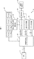
図1は、本発明の一実施の形態に係るメモリアクセス制御システムの構成例を示すブロック図である。同図のメモリアクセス制御システム10は、LPDDRSDRAM29のクロック周波数を、例えば、メモリアクセス制御システム10が搭載された電子機器(例えば、デジタルカメラなど)の動作モードに応じて変更するようになされている。
FIG. 1 is a block diagram showing a configuration example of a memory access control system according to an embodiment of the present invention. The memory
デジタルカメラなど撮像機能、表示機能などを有する電子機器においては、CPUとメインメモリ間のデータ転送の高速化のため、コンピュータ内の各回路間で同期を取る際に、クロック信号の立上がり時と立下がり時の両方を利用し、片方のみを利用する場合に比べ単位時間あたりの処理効率を2倍に高めることができるDDR(Double Data Rate)方式が近年多く採用されている。さらに、DDRを高性能化し、省電力化を図った規格DDR2も提唱されている。 In electronic devices such as digital cameras that have imaging and display functions, the clock signal rises and rises when synchronizing each circuit in the computer to speed up data transfer between the CPU and main memory. In recent years, the DDR (Double Data Rate) method has been widely adopted, which can use both the time of the fall and double the processing efficiency per unit time compared to the case of using only one of them. In addition, DDR2 has been proposed to improve the performance of DDR and save power.
また、例えば、モバイル機器などの用途を考慮して、DDR2をさらに省電力化した規格LPDDR(Low Power Double Data Rate)も提唱されている。LPDDRSDRAM29は、規格LPDDRに適合するメモリとされる。 For example, in consideration of applications such as mobile devices, a standard LPDDR (Low Power Double Data Rate) that further reduces power consumption of DDR2 has been proposed. The LPDDR SDRAM 29 is a memory conforming to the standard LPDDR.
LPDDRSDRAMを搭載する電子機器においては、消費電力を抑制するために、例えば、必要なメモリ容量、電子機器の動作モードなどに応じて、クロック周波数を変更する制御が行われることが一般的である。高速のクロックで電子機器を動作させると、当然単位時間あたりの消費電力量が増えるからである。 In an electronic device equipped with LPDDRSDRAM, in order to reduce power consumption, control for changing a clock frequency is generally performed according to, for example, a required memory capacity, an operation mode of the electronic device, and the like. This is because if the electronic device is operated with a high-speed clock, the power consumption per unit time naturally increases.
このため、図1のメモリアクセス制御システム10は、自分が搭載された電子機器の動作モードに応じてクロック周波数を変更するようになされている。すなわち、メモリアクセス制御システム10は、例えば、デジタルカメラなどの電子機器に搭載されることを想定して構成されている。
For this reason, the memory
同図において、CPU(Central Processing Unit)21は、メモリアクセス制御システム10が搭載された電子機器の中央演算装置であって、実際には、メモリアクセス制御システム10のために設けられるものではない。
In the figure, a CPU (Central Processing Unit) 21 is a central processing unit of an electronic device in which the memory
CPU21は、例えば、図示せぬROM(Read Only Memory)に記憶されているプログラムに従って各種の処理を実行するようになされており、周波数切り替えシーケンサ22に周波数切り替え要求のコマンドを送出する。CPU21は、例えば、メモリアクセス制御システム10が搭載された電子機器の動作モードに応じて周波数を切り換えるように、周波数切り替えシーケンサ22に、周波数切り替え要求のコマンドを送出するようになされている。
The
周波数切り替えシーケンサ(Frequency Change Sequencer)22は、例えば、LSI(Large-Scale Integrated circuit)チップとして構成される。以下、適宜、周波数切り替えシーケンサ22を、FCS22と称することにする。 The frequency change sequencer (Frequency Change Sequencer) 22 is configured as an LSI (Large-Scale Integrated circuit) chip, for example. Hereinafter, the frequency switching sequencer 22 will be referred to as FCS 22 as appropriate.
FCS22は、クロック周波数の変更(切り替え)に関する各種の信号処理を行うようになされており、メモリコントローラ23、DDR-PHY制御部25、およびクロック制御部26に制御信号を出力するようになされている。
The FCS 22 performs various types of signal processing related to the change (switching) of the clock frequency, and outputs control signals to the
また、FCS22は、CPU21からの指令に基づいてメモリアクセス制御システム10が搭載された電子機器の動作モードの検出、およびブランキング時間の検出を行うようになされている。FCS22は、CPU21からの指令に基づいて動作モードの検出、およびブランキング時間の検出を行って、マスタデバイスブロック27から出力される信号に基づいて、上述した制御信号を生成して出力するようになされている。
Further, the FCS 22 detects an operation mode of an electronic device in which the memory
メモリコントローラは、LPDDR SDRAM29に、初期化コマンド、Writeコマンド、Readコマンド、Auto Refreshコマンド、Self Refreshコマンド等のコマンドを生成して投入するようになされている。
The memory controller generates and sends commands such as an initialization command, a Write command, a Read command, an Auto Refresh command, and a Self Refresh command to the
DDR-PHY24は、メモリコントローラ23とLPDDR SDRAM29との間のインタフェース信号のタイミング調整、位相調整などを行う機能ブロックである。DDR-PHY24には、DLL(Delay Locked Loop)とDL(Delay Line)が搭載されている。
The DDR-
DLは、遅延時間の小さい遅延バッファとセレクタの組み合わせにより構成される遅延ライン(Delay Line:DL)により周期信号の位相調整を行うものであり、DLLは、内部回路で使用する内部クロック信号を外部からの基準クロック信号に対して所定の位相を調整する同期遅延ループ(Delay Locked Loop:DLL)回路により、周期信号の位相調整を行うものである。DLLを用いることで精密な位相調整が可能であるが、DLに比べ消費電力が高くなる。 DL adjusts the phase of a periodic signal by a delay line (Delay Line: DL) composed of a combination of a delay buffer with a small delay time and a selector. DLL is an internal clock signal used in an internal circuit. The phase of the periodic signal is adjusted by a synchronous delay loop (DLL) circuit that adjusts a predetermined phase with respect to the reference clock signal from the signal. Precise phase adjustment is possible by using DLL, but power consumption is higher than DL.
したがって、例えば、クロック周波数をより低い周波数に切り替える場合には、DLLを使用せずにDLを用いた方が、消費電力を削減することができる場合がある。 Therefore, for example, when switching the clock frequency to a lower frequency, it may be possible to reduce power consumption by using DL without using DLL.
DDR-PHY24は、例えば、メモリコントローラ23からWriteコマンドとともに書き込みデータを受信した場合、その書き込みデータを、パラレル−シリアル変換し、倍速データ(Double Data Rate)でLPDDR SDRAM29に転送するようになされている。また、DDR-PHY24は、メモリコントローラ23からReadコマンドを受信した場合、DQS(Data Strobe信号)の位相を調整し、LPDDR SDRAM29から読み出したデータをシリアル−パラレル変換し、メモリコントローラ23へ等倍データ(Single Data Rate)で転送を行う。
For example, when the write data is received together with the write command from the
DDR-PHY制御部25は、DDR-PHY24の制御を行う機能ブロックであり、DDR-PHYの初期化、DLLまたはDLの選択、DLLが選択されたときは位相設定、DLが選択されたときは遅延設定を行う機能ブロックである。
The DDR-
クロック制御部26は、例えば、図示せぬクロック発生部を制御してメモリアクセス制御システム10のクロック周波数、またはメモリアクセス制御システム10が搭載された電子機器全体のクロック周波数を制御する機能ブロックである。
The clock control unit 26 is a functional block that controls a clock frequency of the memory
マスタデバイスブロック27は、複数のマスタデバイスを含んで構成される機能ブロックであり、この例では、マスタデバイスブロック27が、マスタデバイスA(図中マスタAと表記)、マスタデバイスB(図中マスタBと表記)、マスタデバイスC(図中マスタCと表記)、およびマスタデバイスD(図中マスタDと表記)を含んで構成されている。
The
調停回路28は、マスタデバイスブロック27のマスタデバイスからのメモリアクセス要求に基づいて、優先順位付け、帯域制御などを行って、メモリコントローラ23との信号の送受信を行う機能ブロックである。すなわち、マスタデバイスA乃至マスタデバイスDのそれぞれは、LPDDRSDRAM29へのデータの書き込み、または読み出しを行う場合、調停回路28を介してメモリコントローラにアクセス要求を送出することになる。
The
上述したように、LPDDRSDRAM29は、DDR-PHY24を介して、メモリコントローラ23との信号の送受信が行われるようになされており、DDR-PHY24には、DLL(Delay Locked Loop)とDL(Delay Line)が搭載されている。このため、メモリアクセス制御システム10において、クロック周波数を切り換える場合、次に述べる処理を行う必要がある。
As described above, the
クロック周波数を切り換える場合、第1の処理として、LPDDRSDRAM29をセルフリフレッシュと称されるモードで稼動させる処理を行う必要がある。
When switching the clock frequency, as a first process, it is necessary to perform a process of operating the
メモリコントローラ23は、メモリアクセス制御システム10が稼動しているとき、LPDDRSDRAM29にRefreshコマンドを供給する。一般に、SDRAMなどのメモリセルに電荷として記憶されるデータを保持するために所定のリフレッシュ周期でリフレッシュ動作を実行する必要があるからである。通常、メモリコントローラ23は、予め設定された所定のインターバルでRefreshコマンドを供給するオートリフレッシュ機能と称される機能が実装されている。
The
しかしながら、クロック周波数を切り換える場合、一定の時間、メモリコントローラ23がDDR-PHY24へのコマンドの供給が行えない状態となる。このため、LPDDRSDRAM29をセルフリフレッシュと称されるモードで稼動させる。これにより、LPDDRSDRAM29は、メモリコントローラ23からRefreshコマンドが供給されなくとも、自身を定期的にリフレッシュするように動作する。従って、クロック周波数を切り換えに先立って、LPDDRSDRAM29をセルフリフレッシュモードで稼動させることで、クロック周波数を切り換えているときも、LPDDRSDRAM29のメモリセルに電荷として記憶されるデータが適切に保持されるようにすることができる。
However, when the clock frequency is switched, the
また、クロック周波数を切り換える場合、第2の処理として、DDR-PHY24の再設定の処理を行う必要がある。クロック周波数が変わることに伴って、DDR-PHY24をリセットし、各種のパラメータなどを再設定する必要があるからである。これにより、例えば、切り換え後のクロック周波数に応じて、DDR-PHY24に搭載されたDLLまたはDLのいずれを用いるかが選択され、その選択結果に応じて、DLLまたはDLに設定すべきパラメータなどが決定される。
Further, when switching the clock frequency, it is necessary to perform a resetting process of the DDR-
さらに、クロック周波数を切り換える場合、第3の処理として、クロック制御部26にクロック周波数を変更させる処理を行う必要がある。 Further, when the clock frequency is switched, it is necessary to perform a process for causing the clock control unit 26 to change the clock frequency as a third process.
さらに、クロック周波数を切り換える場合、第4の処理として、LPDDRSDRAM29のセルフリフレッシュモードでの稼動を解除させる処理を行う必要がある。
Further, when the clock frequency is switched, as a fourth process, it is necessary to perform a process of canceling the operation of the
図1において、FCS22と、CPU21、メモリコントローラ23、DDR-PHY制御部25、クロック制御部26、およびマスタデバイスブロック27とを接続する矢印に付された記号(c1乃至c13)は、それぞれ図2の表に記述された信号に対応している。
In FIG. 1, symbols (c1 to c13) attached to arrows connecting the FCS 22, the
c1は、周波数切り替え要求の信号であり、CPU21からFCS22に送出されるものである。
c1 is a frequency switching request signal that is sent from the
c2は、Self Refresh Enterのコマンドの投入信号であり、FCS22からメモリコントローラ23に供給される。これにより、メモリコントローラ23が、LPDDRSDRAM29を、セルフリフレッシュモードで稼動させる。
c2 is a command input signal for the Self Refresh Enter, and is supplied from the FCS 22 to the
c3は、c2のSelf Refresh Enterのコマンドの投入信号に対する応答信号とされ、メモリコントローラ23から、FCS22に送出される。
c3 is a response signal to the self refresh enter command input signal of c2, and is sent from the
なお、c2とc3は、上述した、クロック周波数を切り換える場合の第1の処理に対応するものである。 Note that c2 and c3 correspond to the above-described first processing when the clock frequency is switched.
c4は、DDR-PHY24のリセット要求の信号であり、FCS22からDDR-PHY制御部25に送出される。これにより、DDR-PHY24は、リセットされる。
c4 is a reset request signal of the DDR-
c5は、c4のDDR-PHY24のリセット要求の信号に対する応答信号とされ、DDR-PHY制御部25からFCS22に送出される。
c5 is a response signal to the reset request signal of the DDR-
なお、c2とc3は、上述した、クロック周波数を切り換える場合の第2の処理の一部に対応するものである。 Note that c2 and c3 correspond to a part of the second processing described above when the clock frequency is switched.
c6は、クロック周波数切り替え要求の信号であり、FCS22からクロック制御部26に送出される。これにより、クロック周波数が変更される。 c6 is a clock frequency switching request signal, and is sent from the FCS 22 to the clock control unit 26. As a result, the clock frequency is changed.
c7は、c6のクロック周波数切り替え要求の信号に対する応答信号とされ、クロック制御部26からFCS22に送出される。 c7 is a response signal to the clock frequency switching request signal of c6, and is sent from the clock control unit 26 to the FCS 22.
なお、c7とc6は、上述した、クロック周波数を切り換える場合の第3の処理に対応するものである。 Note that c7 and c6 correspond to the above-described third processing when the clock frequency is switched.
c8は、DDR-PHYのパラメータ設定要求の信号であり、FCS22からDDR-PHY制御部25に送出される。これにより、例えば、切り換え後のクロック周波数に応じて、DDR-PHY24に搭載されたDLLまたはDLのいずれを用いるかが選択され、その選択結果に応じて、DLLまたはDLに設定すべきパラメータなどが決定される。
c8 is a DDR-PHY parameter setting request signal, and is sent from the FCS 22 to the DDR-
c9は、c8のDDR-PHYのパラメータ設定要求の信号に対する応答信号であり、DDR-PHY制御部25からFCS22に送出される。
c9 is a response signal to the DDR-PHY parameter setting request signal of c8, and is sent from the DDR-
なお、c8とc9は、上述した、クロック周波数を切り換える場合の第2の処理の一部に対応するものである。 Note that c8 and c9 correspond to a part of the second processing described above when the clock frequency is switched.
c10は、Self Refresh Exitのコマンドの投入信号であり、FCS22からメモリコントローラ23に供給される。これにより、メモリコントローラ23が、LPDDRSDRAM29のセルフリフレッシュモードでの稼動を解除する。
c10 is a command input signal for the Self Refresh Exit, and is supplied from the FCS 22 to the
c11は、c10のSelf Refresh Exitのコマンドの投入信号に対する応答信号であり、メモリコントローラ23から、FCS22に送出される。
c11 is a response signal to the command refresh signal of c10, and is sent from the
なお、c10とc11は、上述した、クロック周波数を切り換える場合の第4の処理に対応するものである。 Note that c10 and c11 correspond to the above-described fourth processing when the clock frequency is switched.
c12は、クロック周波数切り替えが終了したことを表す終了通知の信号であり、FCS22からCPU21に送出される。
c12 is an end notification signal indicating that clock frequency switching has ended, and is sent from the FCS 22 to the
なお、図2には、表記されていないが、c13は、マスタデバイスブロック27から供給されるブランキング信号とされる。ブランキング信号については後述する。
Although not shown in FIG. 2, c13 is a blanking signal supplied from the
このようにして、メモリアクセス制御システム10のクロック周波数が切り換えられる。
In this way, the clock frequency of the memory
本発明においては、図2のc2乃至c13の信号は、FCS22、CPU21、メモリコントローラ23、DDR-PHY制御部25、クロック制御部26、およびマスタデバイスブロック27のそれぞれが、ハードウェアとして構成された論理回路などにより生成するようになされている。従って、図2のc1およびc12の信号を除く各信号は、ソフトウェアの処理を介さずに生成されることになる。
In the present invention, the signals c2 to c13 in FIG. 2 are constituted by the hardware of each of the FCS 22, the
従来のクロック周波数の切り換えの処理では、図2のc2、c4、c6、c8、およびc10の信号がソフトウェアにより生成されていた。しかしながら、図2のc2、c4、c6、c8、およびc10の信号をソフトウェアにより生成する場合、周波数変更を行うための制御プログラムが複雑になる。また、周波数変更を行うための制御プログラムを実行するために、命令コードやワークメモリが必要になり、周波数変更を行う処理を実行する際にメモリにアクセスできなくなることがあるため、それらの命令コードをメモリ以外のROMやSRAMなどに保持しておく必要がある。さらに、周波数変更の処理に要する時間が長くなるため、その間のLPDDRSDRAM29へのアクセスの制限に伴う影響が大きくなる。
In the conventional clock frequency switching process, the signals c2, c4, c6, c8, and c10 in FIG. 2 are generated by software. However, when the signals c2, c4, c6, c8, and c10 in FIG. 2 are generated by software, the control program for changing the frequency becomes complicated. In addition, instruction code and work memory are required to execute the control program for changing the frequency, and the memory may become inaccessible when executing the process for changing the frequency. Must be stored in a ROM or SRAM other than memory. Furthermore, since the time required for the frequency change process becomes long, the influence due to the restriction of access to the
本発明によれば、図2のc2、c4、c6、c8、およびc10の信号がソフトウェアの処理を介さずに生成されるので、複雑な制御プログラムを作成する必要がなく、余分なワークメモリも不要となる。また、本発明によれば、周波数変更の処理がソフトウェアを介さずにハードウェアにより実行されるようにしたので、処理に要する時間を短くすることができる。その結果、例えば、周波数変更の処理に伴ってメモリアクセスが制限される時間も短くなり、例えば、周波数変更の処理に伴う、電子機器の機能などへの影響を小さくすることができる。さらに、周波数変更の処理がソフトウェアを介さずにハードウェアにより実行されるようにしたので、周波数切り換え時のCPU21の処理負荷を極力軽減させることができるので、周波数変更に伴う影響を小さくすることができる。
According to the present invention, since the signals c2, c4, c6, c8, and c10 in FIG. 2 are generated without software processing, it is not necessary to create a complicated control program, and extra work memory is also provided. It becomes unnecessary. In addition, according to the present invention, the frequency change process is executed by hardware without using software, so that the time required for the process can be shortened. As a result, for example, the time during which memory access is restricted with the frequency change process is shortened, and for example, the influence on the function of the electronic device associated with the frequency change process can be reduced. Furthermore, since the frequency change processing is executed by hardware without using software, the processing load on the
図3は、メモリアクセス制御システム10におけるクロック周波数の切り替えを説明するタイミングチャートである。同図は、横軸が時間とされ、マスタデバイスA乃至マスタデバイスD(図中、マスタA乃至マスタDと表記)によるLPDDRSDRAM29へのアクセス時間が「メモリアクセス」と記述された長方形の枠により示されている。この例では、マスタデバイスA乃至マスタデバイスDは、全て表示用マスタデバイスなどのリアルタイム系マスタデバイスであるものとする。
FIG. 3 is a timing chart for explaining clock frequency switching in the memory
また、同図において図中最も上の矢印により、メモリアクセス制御システム10が搭載された電子機器のモードが表記されている。すなわち、メモリアクセス制御システム10が搭載された電子機器時刻T1から時刻T2までの時間はモードAで稼動し、時刻T2以後、モードBで稼動していることになる。
Further, in the figure, the uppermost arrow in the figure indicates the mode of the electronic device in which the memory
同図の同期信号は、図中垂直下方向に突出したパルスにより、メモリアクセス制御システム10の同期時刻を特定する信号とされる。
The synchronization signal in the figure is a signal for specifying the synchronization time of the memory
同図のモード検出信号は、上述したモードAとモードBを表す信号であり、FCS22に供給される信号とされる。 The mode detection signal in the figure is a signal representing the above-described mode A and mode B, and is a signal supplied to the FCS 22.
同図のブランキング信号は、マスタデバイスブロック27から供給される信号とされ、図1のc13の信号に対応するものである。リアルタイム系マスタデバイスは、処理の遅延等の発生による影響が大きいマスタデバイスであり、例えば、表示用マスタデバイスは、メモリアクセスが中断されるなどすると、画像を正常に表示することができなくなってしまう。
The blanking signal in the figure is a signal supplied from the
ブランキング信号は、リアルタイム系の表示用マスタデバイスがLPDDRSDRAM29にアクセスしていないタイミングを特定するための信号とされる。この例では、表示用マスタデバイスA乃至マスタデバイスDが、いずれもLPDDRSDRAM29にアクセスしていないとき、ブランキング信号のレベルが高く(「H」)なり、マスタデバイスA乃至マスタデバイスDのいずれかがLPDDRSDRAM29にアクセスしているとき、ブランキング信号のレベルが低く(「L」)なっている。この例では、リアルタイム系マスタデバイスである、マスタデバイスA乃至マスタデバイスDのメモリアクセスが終了したとき(この例では、マスタデバイスBによる第2回目のメモリアクセスが終了したとき)、ブランキング信号のレベルが「H」となっている。
The blanking signal is a signal for specifying the timing when the real-time display master device is not accessing the
この例では、電子機器のモードAは、クロック周波数の高いモードとされ、マスタデバイスA乃至マスタデバイスDのそれぞれがLPDDRSDRAM29にアクセスするモードであるものとする。一方、電子機器のモードBは、マスタデバイスAとマスタデバイスBのみがLPDDRSDRAM29にアクセスするモードであるものとし、CPU21は、電子機器がモードBで稼動する場合、消費電力削減のため、クロック周波数をより低く変更するようになされているものとする。
In this example, it is assumed that the mode A of the electronic device is a mode with a high clock frequency, and each of the master devices A to D accesses the
時刻T1に先立って、CPU21は、FCS22に対して図2を参照して上述した信号c1を送出しておく。すなわち、CPU21は、FCS22に対して、モードBでの稼動時にはクロック周波数を低くするように指令する。この指令を受けてFCS22は、モード検出信号を監視し、現在の稼動モードを検出する。なお、図1と図2においては、モード信号が図示されていないが、例えば、CPU21からc1の信号とは別に、モード検出信号が、FCS22に供給されるものとする。
Prior to time T1, the
時刻T2において、FCS22は、電子機器の稼動モードがモードBに移行したことを検出する。そして、FCS22は、ブランキング信号のレベルが「H」となるまで待機し、時刻T3において、FCS22は、ブランキング信号のレベルが「H」となったことを検出する。 At time T2, the FCS 22 detects that the operation mode of the electronic device has shifted to mode B. The FCS 22 waits until the level of the blanking signal becomes “H”, and at time T3, the FCS 22 detects that the level of the blanking signal becomes “H”.
時刻T3を経過すると、FCS22は、図2を参照して上述したc2、c4、c6、c8、c10、およびc12の信号のそれぞれを出力していく。これにより、図2を参照して上述した一連の処理が行われることになる。図3においては、図2のc2の信号が出力されてから、c12(またはc11)の信号が出力されるまでの時間が「周波数変更期間」として表記されている。 When the time T3 has elapsed, the FCS 22 outputs each of the signals c2, c4, c6, c8, c10, and c12 described above with reference to FIG. As a result, the series of processes described above with reference to FIG. 2 is performed. In FIG. 3, the time from when the signal c2 in FIG. 2 is output until the signal c12 (or c11) is output is expressed as a “frequency change period”.
このように、周波数の変更の処理は、リアルタイム系マスタデバイスによるメモリアクセスが発生しない時間に実行されるようになされている。このようにすることで、例えば、周波数の変更の処理を行っても、画像の表示の乱れなどが発生しないようにすることが可能となる。 As described above, the process of changing the frequency is executed at a time when no memory access by the real-time master device occurs. In this way, for example, even when the frequency change process is performed, it is possible to prevent the image display from being disturbed.
図4は、図3と同様に、メモリアクセス制御システム10におけるクロック周波数の切り替えを説明するタイミングチャートである。同図も、横軸が時間とされ、マスタデバイスA乃至マスタデバイスD(図中、マスタA乃至マスタDと表記)によるLPDDRSDRAM29へのアクセス時間が「メモリアクセス」と記述された長方形の枠により示されている。図4の例では、マスタデバイスA乃至マスタデバイスCは、表示用マスタデバイスなどのリアルタイム系マスタデバイスであるものとし、マスタデバイスDは、リアルタイム系マスタデバイスではないベストエフォート系マスタデバイスであるものとする。
FIG. 4 is a timing chart illustrating switching of the clock frequency in the memory
ベストエフォート系マスタデバイスは、メモリアクセスが中断されるなどした場合でも、影響が小さい処理を行うマスタデバイスである。従って、図4の場合、マスタデバイスDのメモリアクセスが中断されても、電子機器の動作に深刻な影響を与えることはない。 The best-effort master device is a master device that performs a process having a small influence even when a memory access is interrupted. Therefore, in the case of FIG. 4, even if the memory access of the master device D is interrupted, the operation of the electronic device is not seriously affected.
また、図4の例においても図中最も上の矢印により、メモリアクセス制御システム10が搭載された電子機器のモードが表記されている。すなわち、メモリアクセス制御システム10が搭載された電子機器時刻T11から時刻T12までの時間はモードAで稼動し、時刻T12以後、モードBで稼動していることになる。
In the example of FIG. 4 as well, the mode of the electronic device in which the memory
同図の同期信号とモード検出信号は、図3の場合と同様なので詳細な説明は省略する。 Since the synchronization signal and mode detection signal in the figure are the same as those in FIG. 3, a detailed description thereof will be omitted.
図4の例では、ブランキング信号は、時刻T13においてレベルが「H」となっている。時刻T13においては、マスタデバイスDによりメモリアクセスが発生しているが、上述したように、マスタデバイスDは、ベストエフォート系マスタデバイスである。このため、リアルタイム系マスタデバイスである、マスタデバイスA乃至マスタデバイスCのメモリアクセスが終了したとき(この例では、マスタデバイスBによる第2回目のメモリアクセスが終了したとき)、ブランキング信号のレベルが「H」となっている。 In the example of FIG. 4, the level of the blanking signal is “H” at time T13. At time T13, a memory access is generated by the master device D. As described above, the master device D is a best effort master device. Therefore, when the memory access of the master devices A to C, which are real-time master devices, is completed (in this example, when the second memory access by the master device B is completed), the level of the blanking signal Is “H”.
図4の場合も、時刻T11に先立って、CPU21は、FCS22に対して図2を参照して上述した信号c1を送出しておく。すなわち、CPU21は、FCS22に対して、モードBでの稼動時にはクロック周波数を低くするように指令する。この指令を受けてFCS22は、モード検出信号を監視し、現在の稼動モードを検出する。
Also in the case of FIG. 4, prior to time T11, the
時刻T12において、FCS22は、電子機器の稼動モードがモードBに移行したことを検出する。そして、FCS22は、ブランキング信号のレベルが「H」となるまで待機し、時刻T13において、FCS22は、ブランキング信号のレベルが「H」となったことを検出する。 At time T12, the FCS 22 detects that the operation mode of the electronic device has shifted to mode B. Then, FCS 22 waits until the level of the blanking signal becomes “H”, and at time T13, FCS 22 detects that the level of the blanking signal has become “H”.
時刻T13を経過すると、FCS22は、図2を参照して上述したc2、c4、c6、c8、c10、およびc12の信号のそれぞれを出力していく。これにより、図2を参照して上述した一連の処理が行われることになる。図4においては、図2のc2の信号が出力されてから、c12(またはc11)の信号が出力されるまでの時間が「周波数変更期間」として表記されている。 When the time T13 has elapsed, the FCS 22 outputs the signals c2, c4, c6, c8, c10, and c12 described above with reference to FIG. As a result, the series of processes described above with reference to FIG. 2 is performed. In FIG. 4, the time from when the signal c2 in FIG. 2 is output until the signal c12 (or c11) is output is expressed as a “frequency change period”.
このように、周波数の変更の処理は、リアルタイム系マスタデバイスによるメモリアクセスが発生しない時間に実行されるので、例えば、図4の例のように、ベストエフォート系のマスタデバイスによるメモリアクセスが中断されることはあるが、リアルタイム系マスタデバイスによるメモリアクセスが中断されることはない。従って、本発明によれば、例えば、周波数の変更の処理を行っても、画像の表示の乱れなどが発生しないようにすることができる。 As described above, since the frequency change process is executed at a time when the memory access by the real-time master device does not occur, the memory access by the best-effort master device is interrupted, for example, as in the example of FIG. However, the memory access by the real-time master device is not interrupted. Therefore, according to the present invention, for example, even if the process of changing the frequency is performed, it is possible to prevent the image display from being disturbed.
図5は、図4において、「周波数変更期間」として表記されている時間を、さらに詳細に説明するタイミングチャートである。同図は、横軸が時間とされ、図4のマスタデバイスDによるLPDDRSDRAM29へのアクセス時間が「メモリアクセス」と記述された長方形の枠により示されている。
FIG. 5 is a timing chart for explaining in more detail the time represented as “frequency change period” in FIG. 4. In this figure, the horizontal axis represents time, and the access time to the
また、同図においては、ステータスとして、次に述べる時間に対応する枠が記述されている。 In the figure, a frame corresponding to the following time is described as the status.
図2のc2の信号が送出されてからc4の信号が送出されるまでの時間が、「Self Refresh Enter」と記述された長方形の枠により示されている。さらに、図2のc4の信号が送出されてからc6の信号が送出されるまでの時間が、「DDR-PHY Reset」と記述された長方形の枠により示されている。また、図2のc6の信号が送出されてからc8の信号が送出されるまでの時間が、「クロック周波数切り換え」と記述された長方形の枠により示されている。さらに、図2のc8の信号が送出されてからc10の信号が送出されるまでの時間が、「パラメータ設定」と記述された長方形の枠により示されている。また、図2のc10の信号が送出されてからc12の信号が送出されるまでの時間が、「Self Refresh Exit」と記述された長方形の枠により示されている。 The time from when the signal c2 in FIG. 2 is sent to when the signal c4 is sent is indicated by a rectangular frame in which “Self Refresh Enter” is described. Further, the time from when the signal c4 in FIG. 2 is transmitted until the signal c6 is transmitted is indicated by a rectangular frame described as “DDR-PHY Reset”. Also, the time from when the signal c6 in FIG. 2 is transmitted until the signal c8 is transmitted is indicated by a rectangular frame described as “clock frequency switching”. Further, the time from when the signal c8 in FIG. 2 is transmitted until the signal c10 is transmitted is indicated by a rectangular frame in which “parameter setting” is described. Also, the time from when the signal c10 shown in FIG. 2 is sent to when the signal c12 is sent is indicated by a rectangular frame described as “Self Refresh Exit”.
図5に示されるように、ブランキング信号のレベルが「H」となった時刻T13を経過した後、所定の遅延時間があり、その後図2のc2の信号が送出されることになる。そして、c2の信号が送出されたタイミングで、マスタデバイスDによるメモリアクセスは中断される。 As shown in FIG. 5, after a time T13 when the level of the blanking signal becomes “H” has elapsed, there is a predetermined delay time, and then the signal c2 in FIG. 2 is transmitted. Then, the memory access by the master device D is interrupted at the timing when the signal c2 is transmitted.
また、図5に示されるように、図2のc11の信号(c10の信号に対する応答)が送出された後、マスタデバイスDによるメモリアクセスが再開されることになる。 Further, as shown in FIG. 5, the memory access by the master device D is resumed after the signal c11 in FIG. 2 (response to the signal c10) is transmitted.
図6は、図5のステータスをさらに詳細に説明するために、FCS22と、メモリコントローラ23、DDR-PHY制御部25、およびクロック制御部26との間で送受信される各種の要求信号、応答信号を示したタイミングチャートである。
FIG. 6 shows various request signals and response signals transmitted / received between the FCS 22, the
同図の最も上側には、FCS22の動作クロックがパルスとして示されている。 The operation clock of the FCS 22 is shown as a pulse on the uppermost side of the figure.
図6において、時刻T21において第1番目のFCS22の動作クロックが投入された後、所定の遅延時間経過後に、FCS22は、メモリコントローラ23への要求信号が出力される。ここで、出力される要求信号は、図2のc2の信号に対応し、図6においては、信号のレベルが「H」となったことにより、要求信号が出力されたことを表している。
In FIG. 6, after the operation clock of the first FCS 22 is input at the time T21, the FCS 22 outputs a request signal to the
また、メモリコントローラ23は、FCS22からの要求信号が出力されると、自動的に、LPDDRSDRAM29をセルフリフレッシュモードで稼動させるようになされている。
Further, the
メモリコントローラ23への要求信号が出力された後、所定の遅延時間経過後にメモリコントローラ23からFCS22へ応答信号が出力される。ここで、出力される応答信号は、図2のc3の信号に対応し、図6においては、信号のレベルが「H」となったことにより、応答信号が出力されたことを表している。
After a request signal is output to the
メモリコントローラ23からFCS22へ応答信号が出力された後、時刻T22のFCS22の動作クロックのパルスの立ち上がりを待って、DDR-PHY制御部25への要求信号が出力される。ここで、出力される要求信号は、図2のc4の信号に対応し、図6においては、信号のレベルが「H」となったことにより、要求信号が出力されたことを表している。
After the response signal is output from the
DDR-PHY制御部25への要求信号が出力された後、所定の遅延時間経過後にDDR-PHY制御部25からFCS22へ応答信号が出力される。ここで、出力される応答信号は、図2のc5の信号に対応し、図6においては、信号のレベルが「H」となったことにより、応答信号が出力されたことを表している。
After a request signal is output to the DDR-
DDR-PHY制御部25からFCS22へ応答信号が出力された後、時刻T23のFCS22の動作クロックのパルスの立ち上がりを待って、クロック制御部26への要求信号が出力される。ここで、出力される要求信号は、図2のc6の信号に対応し、図6においては、信号のレベルが「H」となったことにより、要求信号が出力されたことを表している。
After a response signal is output from the DDR-
そして、この後、図6の図中下から2番目の信号として示されている電子機器のクロックのパルス幅が広く変更されている。すなわち、電子機器のクロック周波数が高い周波数から低い周波数へ切り換えられたのである。 Thereafter, the pulse width of the clock of the electronic device shown as the second signal from the bottom in the drawing of FIG. 6 is widely changed. That is, the clock frequency of the electronic device is switched from a high frequency to a low frequency.
クロック制御部26への要求信号が出力された後、所定の遅延時間経過後にクロック制御部26からFCS22へ応答信号が出力される。ここで、出力される応答信号は、図2のc7の信号に対応し、図6においては、信号のレベルが「H」となったことにより、応答信号が出力されたことを表している。 After a request signal is output to the clock control unit 26, a response signal is output from the clock control unit 26 to the FCS 22 after a predetermined delay time has elapsed. Here, the output response signal corresponds to the signal c7 in FIG. 2, and in FIG. 6, the response signal is output when the level of the signal becomes “H”.
また、クロック制御部26からFCS22へ応答信号が出力されると、FCS22は、時刻T24のFCS22の動作クロックのパルスの立ち上がりを待って、DDR-PHY制御部25への要求信号の出力を停止し、また、クロック制御部26への要求信号の出力を停止する。図6においては、信号のレベルが「L」となったことにより、要求信号の出力が停止されたことを表している。
When a response signal is output from the clock control unit 26 to the FCS 22, the FCS 22 waits for the rise of the operation clock pulse of the FCS 22 at time T24 and stops outputting the request signal to the DDR-
また、DDR-PHY制御部25への要求信号の出力が停止されたことにより、DDR-PHY24のパラメータ設定が行われることになる。すなわち、FCS22のDDR-PHY制御部25への要求信号の出力の停止は、図2のc8の信号の供給に対応する。
Further, when the output of the request signal to the DDR-
DDR-PHY制御部25への要求信号の出力が停止されてから所定の時間経過後に、DDR-PHY制御部25は、FCS22への応答信号の出力を停止するようになされている。図6においては、信号のレベルが「L」となったことにより、応答信号の出力が停止されたことを表している。DDR-PHY制御部25からFCS22への応答信号の出力の停止が図2のc9に対応することになる。
The DDR-
DDR-PHY制御部25からの応答信号の出力が停止されてから、時刻T25のFCS22の動作クロックのパルスの立ち上がりを待って、FCS22は、メモリコントローラ23への要求信号の出力を停止するようになされている。図6においては、信号のレベルが「L」となったことにより、要求信号の出力が停止されたことを表している。
After the output of the response signal from the DDR-
また、FCS22からメモリコントローラ23への要求信号の出力の停止は、図2のc10の信号の供給に対応する。すなわち、メモリコントローラ23は、FCS22からの要求信号の出力が停止されると、自動的に、LPDDRSDRAM29のセルフリフレッシュモードでの稼動を解除させるようになされている。
Further, the stop of the output of the request signal from the FCS 22 to the
メモリコントローラ23への要求信号の出力が停止されてから所定の時間経過後に、メモリコントローラ23は、FCS22への応答信号の出力を停止するようになされている。図6においては、信号のレベルが「L」となったことにより、応答信号の出力が停止されたことを表している。
The
また、メモリコントローラ23からFCS22への応答信号の出力の停止は、図2のc11の信号の供給に対応する。すなわち、FCS22は、メモリコントローラ23からの応答信号の出力が停止されると、時刻T26のFCSの動作クロックのパルスの立ち上がりを待って、LPDDRSDRAM29のセルフリフレッシュモードでの稼動が解除されたことを認識する。
The stop of the response signal output from the
このようにして、図2を参照して上述した一連の信号が生成されて出力されるようになされている。 In this way, the series of signals described above with reference to FIG. 2 is generated and output.
図7は、本発明を適用した撮像装置70の構成例を示すブロック図である。撮像装置70は、例えば、デジタルカメラとして構成される。
FIG. 7 is a block diagram illustrating a configuration example of an
同図において、撮像素子80は、CCD(Charge Coupled Device)、CMOS(Complementary Metal-Oxide Semiconductor)などの光電変換センサにより構成される。
In the figure, an
前処理部81は、撮像素子80から供給された電気信号の画像情報に対して、CDS(Correlated Double Sampling)処理を行って、S/N比を良好に保つようにするとともに、AGC(Automatic Gain Control)処理を行って、利得を制御し、そして、A/D(Analog/Digital)変換を行って、デジタル信号とされた画像データを生成する。前処理部81のタイミングジェネレータと、Vドライバは、撮像素子80の駆動タイミングを制御する。
The
前処理部81からのデータは、カメラDSP(Digital Signal Processor)部85に供給される。カメラDSP部85は、カメラ信号処理部86、解像度変換部87、画像Codec部88、メモリ制御部89、表示制御部90、メディア制御部91、ARB(arbiter)92、メモリ装置93、LCDモニタ94、記録メディア95、およびFCS100により構成されている。
Data from the preprocessing
カメラ信号処理部86は、前処理部81から供給されたデータに所定の処理を施してイメージ画像データとして出力する。
The camera
解像度変換部87は、カメラ信号処理部86が出力したイメージ画像データの解像度を必要に応じて変換する。
The
画像Codec部88は、カメラ信号処理部86が出力したイメージ画像データを、予め設定された圧縮符号化方式により圧縮符号化するようになされている。
The
メモリ制御部89は、メモリ装置93を制御し、表示制御部90は、LCD(Liquid Crystal Display)モニタ94を制御する。
The
メモリ装置93は、例えば、LPDDRSDRAMにより構成されるものとする。
The
メモリ制御部89には、図1のメモリコントローラ23、DDR-PHY24、DDR-PHY制御部25、クロック制御部26、および調停回路28に対応する機能ブロックが設けられているものとする。
It is assumed that the
また、メモリ制御部89とARB92との間にFCS100が設けられている。FCS100は、図1のFCS22と同様の機能ブロックである。
An
メディア制御部91は、記録メディア95を制御する。記録メディア95は、例えば、半導体メモリを用いたいわゆるメモリカード、記録可能なDVD(Digital Versatile Disk)、磁気ディスクなどにより構成される。
The
ARB92は、CPU97とカメラDSP部85のインタフェースである。そして、CPU97は、操作部96からの供給される信号に基づいて、EEPROM (Electrically Erasable Programmable Read-Only Memory)99からプログラムをロードし、ワークメモリであるRAM(Random Access Memory)98を使用してプログラムを実行し、カメラDSP部85と通信しながら、各種の処理を実行するようになされている。
The
図7の撮像装置70は、例えば、高速撮像を行うための高速撮像モードと、図示せぬレンズから取り込まれた画像をLCDモニタに表示するモニタリングモードで稼動するようになされている。また、撮像装置70は、高速撮像モードにおいて、高周波数のクロックにより動作するようになされており、モニタリングモードでは、低周波数のクロックにより動作するようになされている。
The
図8は、撮像装置70が、モニタリングモードで稼動中に高速撮像モードに変更され、撮像装置のクロックの周波数が低周波数から高周波数に切り換えられる場合の例を説明するタイミングチャートである。
FIG. 8 is a timing chart illustrating an example in which the
撮像装置70におけるモニタリングは、例えば、次のように行われる。
Monitoring in the
前処理部81から供給されたデータをカメラDSP部85に取り込み、カメラ信号処理部86を介して解像度変換部87に供給し、画像のサイズを変更する。そして、サイズが変更された画像データは、メモリ制御部89を介して、メモリ装置93に書き込まれる。このとき、解像度変換部87はモニタリング用のメモリ装置93内の仮想空間であるメモリ空間を2面(メモリ領域1、メモリ領域2)持っており、イメージ画像の1枚目はメモリ領域1に書き込み、2枚目はメモリ領域2に書き込むようになされており、フリップして使用するようになされている。同様に表示制御部90もメモリ領域1、メモリ領域2をフリップして読み出し、LCDモニタ94に出力する。
The data supplied from the preprocessing
撮像装置70における高速撮像は、例えば、次のように行われる。
High-speed imaging in the
操作部96を介して入力されるユーザの指令に基づいて、前処理部81から供給されたデータをカメラDSP部85に取り込み、カメラ信号処理部86を介して解像度変換部87に供給し、画像のサイズを変更する。そして、サイズが変更された画像データは、メモリ制御部89を介して、メモリ装置93に書き込まれる。
Based on a user command input via the
このとき、解像度変換部87はメモリ装置93内の仮想空間であるメモリ空間を4面(メモリ領域1、メモリ領域2、メモリ領域3、メモリ領域4)に設定する。そして、解像度変換部87は、撮像された画像の1枚目はメモリ領域1に書き込み、2枚目はメモリ領域2に書き込み、3枚目はメモリ領域3に書き込み、4枚目はメモリ領域4に書き込み、5枚目はメモリ領域1に書き込むようになされている。
At this time, the
表示制御部90は、解像度変換部87が処理を行ったメモリ領域1とメモリ領域3を交互に読み出し、LCDモニタ94に出力する。画像Codec部88は、解像度変換部87が処理を行って書き込んだデータを、メモリ領域1、メモリ領域2、メモリ領域3、メモリ領域4から順に読み出し、JPEG/MPEGなどのストリームデータに圧縮符号化し、メディア制御部91を介して、記録メディア95に書き込むようになされている。
The
いまの場合、カメラ信号処理部86、解像度変換部87、および表示制御部90は、それぞれリアルタイム系マスタデバイスとなる。なお、解像度変換部87は、モニタリングモードでは、リアルタイム系マスタデバイスとして動作するが、高速撮像モードでは、ベストエフォート系マスタデバイスとして動作するものとする。
In this case, the camera
図8は、撮像装置70におけるクロック周波数の切り替えを説明するタイミングチャートである。同図は、横軸が時間とされ、カメラ信号処理部からのイメージ画像データの供給時間が「イメージ画像」と記述された長方形の枠により表示されている。
FIG. 8 is a timing chart for explaining switching of the clock frequency in the
また、同図において、解像度変換部87によるメモリ領域1、メモリ領域2、メモリ領域3、メモリ領域4へのアクセス時間が、「Read(読み出し)」、または「Write(書き込み)」と記述された長方形の枠により表示されている。
In the same figure, the access time to the memory area 1, the
さらに、同図において、表示制御部90がLCDモニタ94に画像を表示する表示時間が「表示画」と記述された長方形の枠により表示されている。
Further, in the figure, the display time for the
また、同図において、画像Codec部88がデータを圧縮符号化する時間が、「JPEG」と記述された長方形の枠により表示されている。
In the figure, the time for the
また、同図のモード検出信号およびブランキング信号は、図3、または図4を参照して上述したものと同様なので、詳細な説明は省略する。 Further, since the mode detection signal and the blanking signal in the figure are the same as those described above with reference to FIG. 3 or FIG. 4, detailed description thereof will be omitted.
図8においては、時刻T41において、モード検出信号がモニタリングモードから高速撮像モードに変更されたことを表している。 FIG. 8 shows that the mode detection signal is changed from the monitoring mode to the high-speed imaging mode at time T41.
そして、図8のブランキング信号のレベルが「H」となる時刻T42において、クロック周波数の切り替えが行われる。このとき、図2を参照して上述したような信号がFCS100とメモリ制御部89との間で送受信されることにより、低周波数から高周波数へ周波数変更の処理が行われることになる。
Then, at time T42 when the level of the blanking signal in FIG. 8 becomes “H”, the clock frequency is switched. At this time, the signal as described above with reference to FIG. 2 is transmitted and received between the
そして、時刻T43において、撮像装置70が高速撮像モードで動作(高速撮像動作)する。なお、時刻T43までの間、撮像装置70は、モニタリングモードでの動作(モニタリング動作)を続けることになる。
At time T43, the
なお、本明細書において上述した一連の処理は、記載された順序に沿って時系列的に行われる処理はもちろん、必ずしも時系列的に処理されなくとも、並列的あるいは個別に実行される処理をも含むものである。 Note that the series of processes described above in this specification includes processes that are performed in parallel or individually even if they are not necessarily processed in time series, as well as processes that are performed in time series in the order described. Is also included.
10 メモリアクセス制御システム, 21 CPU, 22 周波数切り換えシーケンサ(FCS), 23 メモリコントローラ, 24 DDR-PHY, 25 DDR-PHY制御部, 26 クロック制御部, 27 マスタデバイスブロック, 29 LPDDRSDRAM, 70 撮像装置, 86 カメラ信号処理部, 87 解像度変換部, 88 画像Codec部, 89 メモリ制御部 90 表示制御部, 92 ARB, 23 メモリ装置, 94 LCDモニタ, 97 CPU, 100 FCS 10 memory access control system, 21 CPU, 22 frequency switching sequencer (FCS), 23 memory controller, 24 DDR-PHY, 25 DDR-PHY control unit, 26 clock control unit, 27 master device block, 29 LPDDRSDRAM, 70 imaging device, 86 camera signal processing unit, 87 resolution conversion unit, 88 image codec unit, 89 memory control unit, 90 display control unit, 92 ARB, 23 memory device, 94 LCD monitor, 97 CPU, 100 FCS
Claims (4)
前記メモリコントローラから供給される前記要求信号に対する応答信号に基づいて、前記メモリコントローラと前記メモリとの間のインタフェース信号のタイミング調整を行うDDR-PHYのリセットの要求信号を、前記DDR-PHYを制御するDDR-PHY制御部に出力し、
前記DDR-PHY制御部から供給される前記要求信号に対する応答信号に基づいて、クロック信号の周波数を制御するクロック制御部に、クロック周波数の切り替えの要求信号を出力し、
前記クロック制御部から供給される前記要求信号に対する応答信号に基づいて、切り換え後のクロック周波数に応じた前記DDR-PHYのパラメータの設定の要求信号を、DDR-PHY制御部に出力し、
前記DDR-PHY制御部から供給される前記要求信号に対する応答信号に基づいて、前記メモリのセルフリフレッシュモードでの稼動の解除制御させる要求信号を、前記メモリコントローラに出力することで、前記DDR方式を採用したメモリのクロック周波数を変更する
メモリアクセス制御装置。 A request signal that causes the memory controller that controls the memory to control the operation of the memory in the self-refresh mode based on a blanking signal that indicates whether or not the memory adopting the DDR (Double Data Rate) method by the master device is accessed. Output
Based on a response signal to the request signal supplied from the memory controller, the DDR-PHY reset request signal for adjusting a timing of an interface signal between the memory controller and the memory is controlled. Output to the DDR-PHY controller
Based on a response signal to the request signal supplied from the DDR-PHY control unit, to output a clock frequency switching request signal to the clock control unit that controls the frequency of the clock signal,
Based on a response signal to the request signal supplied from the clock control unit, a request signal for setting the DDR-PHY parameters according to the clock frequency after switching is output to the DDR-PHY control unit,
Based on a response signal to the request signal supplied from the DDR-PHY control unit, a request signal for controlling the release of operation of the memory in the self-refresh mode is output to the memory controller. A memory access control device that changes the clock frequency of the adopted memory.
前記電子機器の中央処理装置から周波数変更の要求信号が出力された場合、前記DDR方式を採用したメモリのクロック周波数の変更を行い、前記周波数の変更が完了したとき、前記周波数の変更の完了を通知する信号を、前記中央処理装置に出力する
請求項1に記載のメモリアクセス制御装置。 Mounted on an electronic device having a plurality of the master devices,
When a frequency change request signal is output from the central processing unit of the electronic device, the clock frequency of the memory adopting the DDR method is changed, and when the frequency change is completed, the change of the frequency is completed. The memory access control device according to claim 1, wherein a signal to be notified is output to the central processing unit.
前記DDR方式を採用したメモリのクロック周波数の変更を行う
請求項2に記載のメモリアクセス制御装置。 Among the plurality of master devices, a real-time master device that is greatly affected by the occurrence of processing delay specifies the time when the memory that adopts the DDR method is not accessed based on the blanking signal,
The memory access control device according to claim 2, wherein a clock frequency of a memory adopting the DDR system is changed.
前記撮像された画像の表示に関する処理を行うマスタデバイスと、
前記マスタデバイスが処理するデータを記憶するDDR方式を採用したメモリと、
中央処理装置からの指令に基づいて前記DDR方式を採用したメモリの周波数を変更するメモリアクセス制御装置とを備え、
前記メモリアクセス制御装置は、
前記マスタデバイスによる前記メモリに対するアクセスの有無を表すブランキング信号に基づいて、前記メモリを制御するメモリコントローラに、前記メモリのセルフリフレッシュモードでの稼動を制御させる要求信号を出力し、
前記メモリコントローラから供給される前記要求信号に対する応答信号に基づいて、前記メモリコントローラと前記メモリとの間のインタフェース信号のタイミング調整を行うDDR-PHYのリセットの要求信号を、前記DDR-PHYを制御するDDR-PHY制御部に出力し、
前記DDR-PHY制御部から供給される前記要求信号に対する応答信号に基づいて、クロック信号の周波数を制御するクロック制御部に、クロック周波数の切り替えの要求信号を出力し、
前記クロック制御部から供給される前記要求信号に対する応答信号に基づいて、切り換え後のクロック周波数に応じた前記DDR-PHYのパラメータの設定の要求信号を、DDR-PHY制御部に出力し、
前記DDR-PHY制御部から供給される前記要求信号に対する応答信号に基づいて、前記メモリのセルフリフレッシュモードでの稼動の解除制御させる要求信号を、前記メモリコントローラに出力することで、前記DDR方式を採用したメモリのクロック周波数を変更する
撮像装置。 An imaging means for capturing an image;
A master device that performs processing related to display of the captured image;
A memory adopting a DDR system for storing data processed by the master device;
A memory access control device that changes the frequency of the memory adopting the DDR system based on a command from the central processing unit;
The memory access control device includes:
Based on a blanking signal indicating the presence or absence of access to the memory by the master device, the memory controller that controls the memory outputs a request signal that controls the operation of the memory in a self-refresh mode,
Based on a response signal to the request signal supplied from the memory controller, the DDR-PHY reset request signal for adjusting a timing of an interface signal between the memory controller and the memory is controlled. Output to the DDR-PHY controller
Based on a response signal to the request signal supplied from the DDR-PHY control unit, to output a clock frequency switching request signal to the clock control unit that controls the frequency of the clock signal,
Based on a response signal to the request signal supplied from the clock control unit, a request signal for setting the DDR-PHY parameters according to the clock frequency after switching is output to the DDR-PHY control unit,
Based on a response signal to the request signal supplied from the DDR-PHY control unit, a request signal for controlling the release of operation of the memory in the self-refresh mode is output to the memory controller. An imaging device that changes the clock frequency of the adopted memory.
Priority Applications (2)
| Application Number | Priority Date | Filing Date | Title |
|---|---|---|---|
| JP2008177846A JP4517312B2 (en) | 2008-07-08 | 2008-07-08 | Memory access control device and imaging device |
| US12/487,124 US8068150B2 (en) | 2008-07-08 | 2009-06-18 | Memory access control apparatus and image pickup apparatus |
Applications Claiming Priority (1)
| Application Number | Priority Date | Filing Date | Title |
|---|---|---|---|
| JP2008177846A JP4517312B2 (en) | 2008-07-08 | 2008-07-08 | Memory access control device and imaging device |
Publications (2)
| Publication Number | Publication Date |
|---|---|
| JP2010020387A true JP2010020387A (en) | 2010-01-28 |
| JP4517312B2 JP4517312B2 (en) | 2010-08-04 |
Family
ID=41504813
Family Applications (1)
| Application Number | Title | Priority Date | Filing Date |
|---|---|---|---|
| JP2008177846A Expired - Fee Related JP4517312B2 (en) | 2008-07-08 | 2008-07-08 | Memory access control device and imaging device |
Country Status (2)
| Country | Link |
|---|---|
| US (1) | US8068150B2 (en) |
| JP (1) | JP4517312B2 (en) |
Cited By (8)
| Publication number | Priority date | Publication date | Assignee | Title |
|---|---|---|---|---|
| JP2009146541A (en) * | 2007-12-17 | 2009-07-02 | Fujitsu Microelectronics Ltd | System device and operating method of system device |
| JP2012221443A (en) * | 2011-04-14 | 2012-11-12 | Seiko Epson Corp | Controller, electronic apparatus and image processing system |
| JP2012221442A (en) * | 2011-04-14 | 2012-11-12 | Seiko Epson Corp | Circuit, electronic apparatus and image processing system |
| JP2014504064A (en) * | 2010-11-22 | 2014-02-13 | アップル インコーポレイテッド | Mechanism for efficient DLL training protocol during frequency changes |
| KR101803284B1 (en) | 2016-11-15 | 2017-12-04 | 인천대학교 산학협력단 | Method and apparatus for memory usage based device frequency adjustment |
| JP2018528510A (en) * | 2015-07-31 | 2018-09-27 | クアルコム,インコーポレイテッド | System, method and apparatus for frequency reset of memory |
| JP2019053727A (en) * | 2017-09-15 | 2019-04-04 | 三星電子株式会社Samsung Electronics Co.,Ltd. | Memory unit and memory system including the same |
| JP2021120909A (en) * | 2017-06-30 | 2021-08-19 | ルネサスエレクトロニクス株式会社 | Semiconductor integrated circuit |
Families Citing this family (15)
| Publication number | Priority date | Publication date | Assignee | Title |
|---|---|---|---|---|
| US8533538B2 (en) * | 2010-06-28 | 2013-09-10 | Intel Corporation | Method and apparatus for training a memory signal via an error signal of a memory |
| US8897084B2 (en) | 2011-09-08 | 2014-11-25 | Apple Inc. | Dynamic data strobe detection |
| CN103024257A (en) * | 2011-09-28 | 2013-04-03 | 华晶科技股份有限公司 | Image capturing device capable of automatically switching clock rate of memory and control method of image capturing device |
| KR101965125B1 (en) | 2012-05-16 | 2019-08-28 | 삼성전자 주식회사 | SoC FOR PROVIDING ACCESS TO SHARED MEMORY VIA CHIP-TO-CHIP LINK, OPERATION METHOD THEREOF, AND ELECTRONIC SYSTEM HAVING THE SAME |
| EP2668945A1 (en) * | 2012-06-01 | 2013-12-04 | Bayer Technology Services GmbH | Genotype and phenotype-based medicinal formulations |
| US8874973B2 (en) * | 2012-10-26 | 2014-10-28 | Lsi Corporation | Methods and structure to assure data integrity in a storage device cache in the presence of intermittent failures of cache memory subsystem |
| US9733957B2 (en) | 2014-09-05 | 2017-08-15 | Qualcomm Incorporated | Frequency and power management |
| TWI705666B (en) * | 2015-06-15 | 2020-09-21 | 日商新力股份有限公司 | Transmission device, receiving device, communication system |
| US10169262B2 (en) | 2015-07-14 | 2019-01-01 | Qualcomm Incorporated | Low-power clocking for a high-speed memory interface |
| CN107132904B (en) | 2016-02-29 | 2020-12-15 | 华为技术有限公司 | Control system and control method of DDR system |
| WO2018095084A1 (en) | 2016-11-23 | 2018-05-31 | Zhejiang Dahua Technology Co., Ltd. | System and method for establishing connection between devices |
| CN106534691B (en) * | 2016-11-23 | 2019-03-26 | 浙江大华技术股份有限公司 | One mode adaptive matching method and equipment |
| CN106534788B (en) * | 2016-11-23 | 2019-03-26 | 浙江大华技术股份有限公司 | Mode adaptive matching process, equipment and system in a kind of monitoring system |
| US10057523B1 (en) | 2017-02-13 | 2018-08-21 | Alexander Krymski | Image sensors and methods with multiple phase-locked loops and serializers |
| CN109101073B (en) * | 2017-06-20 | 2023-01-10 | 深圳市中兴微电子技术有限公司 | Bus dynamic frequency modulation method and bus dynamic frequency modulation device |
Citations (3)
| Publication number | Priority date | Publication date | Assignee | Title |
|---|---|---|---|---|
| JPH10320976A (en) * | 1997-05-14 | 1998-12-04 | Fujitsu Ltd | Semiconductor device and its access time adjustment method |
| JP2005115906A (en) * | 2003-09-19 | 2005-04-28 | Ricoh Co Ltd | Memory drive system |
| JP2007310549A (en) * | 2006-05-17 | 2007-11-29 | Sony Corp | Memory control device |
Family Cites Families (6)
| Publication number | Priority date | Publication date | Assignee | Title |
|---|---|---|---|---|
| US7174467B1 (en) * | 2001-07-18 | 2007-02-06 | Advanced Micro Devices, Inc. | Message based power management in a multi-processor system |
| US7003638B2 (en) * | 2002-12-11 | 2006-02-21 | Standard Microsystems Corporation | Memory bus interface for use in a peripheral device |
| JP2005094294A (en) | 2003-09-17 | 2005-04-07 | Fuji Xerox Co Ltd | Coding apparatus and coding program |
| US7308526B2 (en) * | 2004-06-02 | 2007-12-11 | Intel Corporation | Memory controller module having independent memory controllers for different memory types |
| US7360052B2 (en) * | 2005-09-21 | 2008-04-15 | Inventec Corporation | Computer platform memory access control method and system with memory configuration automatic setting capability |
| JP2008257776A (en) * | 2007-04-03 | 2008-10-23 | Elpida Memory Inc | Semiconductor storage device and control method thereof |
-
2008
- 2008-07-08 JP JP2008177846A patent/JP4517312B2/en not_active Expired - Fee Related
-
2009
- 2009-06-18 US US12/487,124 patent/US8068150B2/en not_active Expired - Fee Related
Patent Citations (3)
| Publication number | Priority date | Publication date | Assignee | Title |
|---|---|---|---|---|
| JPH10320976A (en) * | 1997-05-14 | 1998-12-04 | Fujitsu Ltd | Semiconductor device and its access time adjustment method |
| JP2005115906A (en) * | 2003-09-19 | 2005-04-28 | Ricoh Co Ltd | Memory drive system |
| JP2007310549A (en) * | 2006-05-17 | 2007-11-29 | Sony Corp | Memory control device |
Cited By (11)
| Publication number | Priority date | Publication date | Assignee | Title |
|---|---|---|---|---|
| JP2009146541A (en) * | 2007-12-17 | 2009-07-02 | Fujitsu Microelectronics Ltd | System device and operating method of system device |
| JP2014504064A (en) * | 2010-11-22 | 2014-02-13 | アップル インコーポレイテッド | Mechanism for efficient DLL training protocol during frequency changes |
| JP2012221443A (en) * | 2011-04-14 | 2012-11-12 | Seiko Epson Corp | Controller, electronic apparatus and image processing system |
| JP2012221442A (en) * | 2011-04-14 | 2012-11-12 | Seiko Epson Corp | Circuit, electronic apparatus and image processing system |
| US8909965B2 (en) | 2011-04-14 | 2014-12-09 | Seiko Epson Corporation | Circuit, electronic device, and image processing device |
| JP2018528510A (en) * | 2015-07-31 | 2018-09-27 | クアルコム,インコーポレイテッド | System, method and apparatus for frequency reset of memory |
| KR101803284B1 (en) | 2016-11-15 | 2017-12-04 | 인천대학교 산학협력단 | Method and apparatus for memory usage based device frequency adjustment |
| JP2021120909A (en) * | 2017-06-30 | 2021-08-19 | ルネサスエレクトロニクス株式会社 | Semiconductor integrated circuit |
| JP7075528B2 (en) | 2017-06-30 | 2022-05-25 | ルネサスエレクトロニクス株式会社 | Semiconductor integrated circuit |
| JP2019053727A (en) * | 2017-09-15 | 2019-04-04 | 三星電子株式会社Samsung Electronics Co.,Ltd. | Memory unit and memory system including the same |
| JP7316031B2 (en) | 2017-09-15 | 2023-07-27 | 三星電子株式会社 | Memory device and memory system including the same |
Also Published As
| Publication number | Publication date |
|---|---|
| US20100007770A1 (en) | 2010-01-14 |
| JP4517312B2 (en) | 2010-08-04 |
| US8068150B2 (en) | 2011-11-29 |
Similar Documents
| Publication | Publication Date | Title |
|---|---|---|
| JP4517312B2 (en) | Memory access control device and imaging device | |
| US7877531B2 (en) | Image processing apparatus and image processing apparatus controlling method | |
| TWI654523B (en) | Integrated circuit chip,electronic device and memory accessing method | |
| JP5082727B2 (en) | Storage control device, storage control method, and computer program | |
| JP2007310549A (en) | Memory control device | |
| US20030142217A1 (en) | Digital camera | |
| JP2007037112A (en) | Imaging serial interface rom integrated circuit | |
| US10362216B2 (en) | Image pickup apparatus of which display start timing and display quality are selectable, method of controlling the same | |
| JP5274205B2 (en) | Image processing apparatus and image processing apparatus control method | |
| JP2009282721A (en) | Memory controller, memory control system, and method of controlling amount of delay in memory | |
| JP2006343946A (en) | Memory access controller, and computer program | |
| JP7130377B2 (en) | Image processing device | |
| US9286018B2 (en) | Image processing device for improved access efficiency | |
| JP2021184576A (en) | Imaging device and method for controlling imaging device | |
| JP2009163582A (en) | Memory controller and memory system | |
| US11537299B2 (en) | Local memory use for perspective transform engine | |
| JP2006164323A (en) | Refresh control circuit for dram | |
| JP5392606B2 (en) | Image processing apparatus, memory control method, program, and recording medium | |
| JP4934578B2 (en) | Portable electronic device and operation clock control method | |
| JP4666980B2 (en) | Data processing device | |
| JP2020030521A (en) | Image processing apparatus | |
| JP6494441B2 (en) | Image processing apparatus, image processing method, and program | |
| JP2009104529A (en) | Information processor, recording device of moving image with sound, and information processing method | |
| JP2004151877A (en) | Direct memory access controller, memory arbiter, and memory controller therewith | |
| JP2020091696A (en) | Recording and reproducing apparatus |
Legal Events
| Date | Code | Title | Description |
|---|---|---|---|
| A977 | Report on retrieval |
Free format text: JAPANESE INTERMEDIATE CODE: A971007 Effective date: 20100412 |
|
| TRDD | Decision of grant or rejection written | ||
| A01 | Written decision to grant a patent or to grant a registration (utility model) |
Free format text: JAPANESE INTERMEDIATE CODE: A01 Effective date: 20100422 |
|
| A01 | Written decision to grant a patent or to grant a registration (utility model) |
Free format text: JAPANESE INTERMEDIATE CODE: A01 |
|
| A61 | First payment of annual fees (during grant procedure) |
Free format text: JAPANESE INTERMEDIATE CODE: A61 Effective date: 20100505 |
|
| FPAY | Renewal fee payment (event date is renewal date of database) |
Free format text: PAYMENT UNTIL: 20130528 Year of fee payment: 3 |
|
| R250 | Receipt of annual fees |
Free format text: JAPANESE INTERMEDIATE CODE: R250 |
|
| R250 | Receipt of annual fees |
Free format text: JAPANESE INTERMEDIATE CODE: R250 |
|
| LAPS | Cancellation because of no payment of annual fees |