JP2010020120A - Optical filter - Google Patents
Optical filter Download PDFInfo
- Publication number
- JP2010020120A JP2010020120A JP2008180898A JP2008180898A JP2010020120A JP 2010020120 A JP2010020120 A JP 2010020120A JP 2008180898 A JP2008180898 A JP 2008180898A JP 2008180898 A JP2008180898 A JP 2008180898A JP 2010020120 A JP2010020120 A JP 2010020120A
- Authority
- JP
- Japan
- Prior art keywords
- layer
- optical filter
- block
- blocks
- substrate
- Prior art date
- Legal status (The legal status is an assumption and is not a legal conclusion. Google has not performed a legal analysis and makes no representation as to the accuracy of the status listed.)
- Granted
Links
Images


Abstract
Description
本発明は、光を透過、又は光の反射を防止する光学部品、例えば撮影カメラにおいて使用される帯域制限フィルター、入射光線を透過する窓(光学窓)、レンズ等の光学部品に関する。 The present invention relates to an optical component that transmits light or prevents reflection of light, such as a band limiting filter used in a photographing camera, a window (optical window) that transmits incident light, and a lens.
発光装置、受光装置、又は撮影装置などにおいて、光学部品(例えば、光学フィルター)は、該光学部品を透過する光に対して高い透過率を示すことが要求される。そのために、光学部品を構成する材料として、一般に、対象とする波長域の光に対して低い吸収率を有するものが選択される。また、光学部品を構成する材料の屈折率と該光学部品に接する媒質(通常は空気)の屈折率との差に基づいて光学部品の表面(入射面と透過面)で発生する透過率の損失を減少するために、光学部品の表面に反射防止膜を設けることもある。 In a light emitting device, a light receiving device, a photographing device, or the like, an optical component (for example, an optical filter) is required to exhibit a high transmittance with respect to light transmitted through the optical component. Therefore, a material having a low absorptance with respect to light in a target wavelength region is generally selected as a material constituting the optical component. Further, the loss of transmittance generated on the surface (incident surface and transmission surface) of the optical component based on the difference between the refractive index of the material constituting the optical component and the refractive index of the medium (usually air) in contact with the optical component. In order to reduce this, an antireflection film may be provided on the surface of the optical component.
例えば、従来の赤外線用の光学フィルターは、光学フィルターの窓材としてGe、ZnS、ZnSe及びSiなどが良く利用され、また、反射防止膜として、金属フッ化物などが採用されていた(例えば、特許文献3参照)。 For example, in the conventional infrared optical filter, Ge, ZnS, ZnSe, Si, or the like is often used as a window material of the optical filter, and a metal fluoride or the like is employed as an antireflection film (for example, patents). Reference 3).
また、光学部品の表面に反射防止膜を形成する代わりに、その表面に光の波長よりも小さな間隔をあけて規則的な三次元構造を微細加工することにより、この光学部品の表面に反射防止機能を与える試みがあった(例えば、特許文献1〜2、非特許文献1参照)。
Also, instead of forming an antireflection film on the surface of the optical component, the surface of the optical component is antireflective by microfabricating a regular three-dimensional structure with a space smaller than the wavelength of light on the surface. There have been attempts to provide functions (see, for example,
近年、撮影装置の高機能化や高効率化の要求が増してきており、これに答えるべく撮影装置が取扱う光学波長帯をマルチバンド化する必要が出てきた。ところが、上記のような多層の反射防止膜を光学部品に適用する場合には、光学部品が使用される環境(例えば、高温、ヒートサイクル)を考慮して、膜の屈折率や膜の線膨張係数などの材料特性を考慮して膜の材質を選択する必要があった。つまり、設計仕様を越えた環境下で使用されると、反射防止膜の剥離や残留歪み、反射防止膜からの残留ガスの放出といった現象が長期信頼性を阻害するおそれがあった。また、バンドパスフィルターとして急峻な波長選択性を持たせる場合には層数がさらに増加するので、かかる材質選択の問題のために使用環境が制約される課題もあった。 In recent years, there has been an increasing demand for higher functionality and higher efficiency of imaging devices, and in order to answer this, it has become necessary to make the optical wavelength band handled by imaging devices multiband. However, when the multilayer antireflection film as described above is applied to an optical component, the refractive index of the film or the linear expansion of the film is taken into consideration in the environment (for example, high temperature, heat cycle) in which the optical component is used. It was necessary to select the material of the film in consideration of material characteristics such as coefficient. That is, when used in an environment that exceeds the design specifications, phenomena such as peeling of the antireflection film, residual distortion, and release of residual gas from the antireflection film may hinder long-term reliability. In addition, when the band pass filter has a steep wavelength selectivity, the number of layers further increases, and there is a problem that the use environment is restricted due to the problem of the material selection.
他方、特許文献1に示されたような、光学部品の表面に微細な凹凸を形成して反射防止効果を狙う構造では、所望の波長帯を急峻な波長選択性をもって選択することが要求されるマルチバンドの光学フィルターを得ることは特に難しかった。
On the other hand, in a structure in which fine irregularities are formed on the surface of an optical component as shown in
本発明は、上記のような問題点を解決するためになされたものであり、信頼性に優れた波長選択性の良い光学フィルターを提供することを目的とする。 The present invention has been made to solve the above-described problems, and an object of the present invention is to provide an optical filter having excellent wavelength selectivity and excellent reliability.
本発明に係る光学フィルターは、基板と、その基板の主面とこの主面から所定の距離離れた面とで規定される上層内に、光学フィルターが対象とする光を透過し且つ光の波長よりも小さいブロックであって距離をその厚みとするブロックからなるブロック群と、上層に隣接して主面から所定の第二の距離離れた面と上層の表面とで規定される中層内に中層の厚みをその厚みとするブロックからなるブロック群とから構成され、主面を平面視したときのブロック群の占有面積とそれ以外の面積との比率が各層内でそれぞれ所定の比率となるように、ブロックがそれぞれの層内で配置されたことを特徴とする。 The optical filter according to the present invention transmits light targeted by the optical filter and has a wavelength of light in an upper layer defined by a substrate, a main surface of the substrate, and a surface separated from the main surface by a predetermined distance. A middle layer within a middle layer defined by a block group consisting of blocks having a thickness smaller than that of the block, a surface adjacent to the upper layer and a predetermined second distance away from the main surface, and the surface of the upper layer A block group consisting of blocks having the thickness of the block, and the ratio of the occupied area of the block group and the other area when the main surface is viewed in plan is a predetermined ratio in each layer. The blocks are arranged in each layer.
また、本発明に係る光学フィルターは、光学フィルターの基板に、光学フィルターが対象とする光の波長λよりも小さい開口の穴であって、この基板の主面から所定の深さで掘り込んだ複数の穴を所定の深さ毎に複数群備え、主面を平面視して所定の深さ毎に、その深さで複数の穴が占有する面積と穴以外の基板の残地の面積との比率がそれぞれ所定の比率となるように、基板に穴が配設されたことを特徴とするものである。 Moreover, the optical filter according to the present invention is a hole having an opening smaller than the wavelength λ of light targeted by the optical filter, and is dug into the substrate of the optical filter at a predetermined depth from the main surface of the substrate. A plurality of holes are provided for each predetermined depth, and the area occupied by the plurality of holes at the depth and the remaining area of the substrate other than the holes are provided for each predetermined depth in plan view of the main surface. In this case, holes are provided in the substrate so that the ratios of the two are predetermined ratios.
この発明によれば、基板表面に多層構造となる3次元構造体であって、各層における構造体の充填率と、各層の厚みを所定の値にすることにより所望の透過率特性を得ることができる。また、多層積層膜に起因する剥離等の問題も無く、信頼性に優れた波長選択性の良い光学フィルターを得ることができる。 According to the present invention, a three-dimensional structure having a multilayer structure on the surface of the substrate can obtain desired transmittance characteristics by setting the filling rate of the structure in each layer and the thickness of each layer to predetermined values. it can. Moreover, there is no problem such as peeling due to the multilayer laminated film, and an optical filter having excellent reliability and excellent wavelength selectivity can be obtained.
実施の形態1.
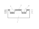
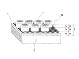
図1は、本実施の形態1に係る光学フィルターの概略構成を示す斜視図である。図2は、斜視図で示した図1を平面視した模式図である。図3は、図2中に示すIII-III線に沿った光学フィルターの断面の模式図である。
FIG. 1 is a perspective view showing a schematic configuration of the optical filter according to the first embodiment. FIG. 2 is a schematic view of FIG. 1 shown in a perspective view in plan view. FIG. 3 is a schematic view of a cross section of the optical filter taken along the line III-III shown in FIG.
以下に、図面を参照しながら、赤外線検出器用の光学フィルターを例にとり、本発明の好適な実施の形態について説明する。なお、以下の説明では、3〜5μm帯及び8〜12μm帯に対応するマルチバンドの光学フィルターを例に本願発明を説明するが、他の形態も、当然に本願発明の技術的範囲に含まれる。また赤外線の波長帯にとどまることなくそれ以外の波長帯の光に対しても有効である。 Hereinafter, preferred embodiments of the present invention will be described with reference to the drawings, taking an optical filter for an infrared detector as an example. In the following description, the present invention will be described by taking a multiband optical filter corresponding to the 3-5 μm band and the 8-12 μm band as an example, but other forms are naturally included in the technical scope of the present invention. . It is also effective for light in other wavelength bands without being limited to the infrared wavelength band.
まず、光学フィルター1の全体構成について説明する。
図1において、光学フィルター1は、基板2の上に配置された下層小円柱31と大円柱4、さらに大円柱4の上に配置された上層小円柱11から構成されている。また、これらの大小の円柱の組合わせを便宜的に表面3次元構造体3と呼ぶことにする。また、基板2、大円柱4等の材質は赤外線を透過するSiである。なお、Siの替わりにGe,ZnSeあるいはこれらの複合材料も基板として使用できる。
First, the overall configuration of the
In FIG. 1, the
図3を参照して、上述した表面3次元構造体3は、基板2に近いほうから順に、下層構造体30、中層構造体20、上層構造体10の3層構造となっている。また、表面3次元構造体3は、光学特性上は等価的に3層の光学多層膜と考えることができる。以下、この理由を説明する。
With reference to FIG. 3, the surface three-
まず、表面3次元構造体3が単層の場合、すなわち基板2の上に単に下層小円柱31のみが配置されている状態(大円柱4は無い状態)を考え、光学フィルターの特性を決める屈折率が表面3次元構造体の形状で決まることを説明する。
光学部品(ここでは光学フィルター)が、ある媒質(通常は空気)に接して配置されるとき、光透過面で入射光線の散乱が発生しないためには、全ての3次元構造体(ここでは下層小円柱31)の間隔Lは入射光線の波長以下になるように設計する。このような3次元構造体において凹部と凸部との面積比率(ここでは、下層小円柱31の上底面の面積を凸部の面積、基板2の上の下層小円柱31が占有していない部分を凹部の面積、として考える)によりその層の実効的な屈折率(nx)を制御することができる。基板2の空気によって満たされている凹部分の面積比率をf(全て凹部の場合をf=1とする)とする場合には、この単層の実効的な屈折率(nx)を式(1)から求めることができる。

When an optical component (here, an optical filter) is disposed in contact with a certain medium (usually air), all three-dimensional structures (here, lower layers) are used in order to prevent scattering of incident light on the light transmission surface. The distance L between the small cylinders 31) is designed to be equal to or smaller than the wavelength of the incident light. In such a three-dimensional structure, the area ratio between the concave portion and the convex portion (here, the area of the upper bottom surface of the lower
上述のように、(1)式に従い単層の屈折率を計算できるので、三層からなる表面3次元構造体3の場合は、上層〜下層構造体の各層毎にそれぞれ屈折率を計算することができる。図3のような3次元構造に当てはめて考えると、面積比率fが上層からf1、f2、f3とする3層構造とすることができる。この場合の実効的な屈折率(nx)は、各層によって異なりそれぞれn1、n2、n3となる。このように、面積比率fを変えることによって、ステップ状に屈折率が変化する多層膜を積層した場合と同等の効果を得ることができる。また面積比率fで実効的な屈折率(nx)が確定することから、例えば下層小円柱31をランダムに配置してもよく、特に凹凸部分を周期構造とする必要は無い。
As described above, since the refractive index of a single layer can be calculated according to the equation (1), in the case of a three-layer surface three-
つぎに、上述した単層の波長ピークは、実効的屈折率部分の凸部の高さ(すなわち、凹部の深さ:d)によって式(2)から決定される。
したがって、目的とする赤外線を透過したい波長帯を計算するには、上記(1)式を用いて各層構造体毎に屈折率(nx)を算出し、透過したい波長帯に合わせて(2)式を用いて上層〜下層構造体の各層構造体の厚み(dx)を求めることができる。 Therefore, in order to calculate the target wavelength band in which infrared rays are desired to be transmitted, the refractive index (n x ) is calculated for each layer structure using the above equation (1), and the wavelength band desired to be transmitted is adjusted to (2). The thickness (d x ) of each layer structure of the upper layer to the lower layer structure can be obtained using the formula.
3〜5μm帯及び8〜14μm帯に対応するマルチバンドの光学フィルターを設計する場合は、(1)式、(2)式を基に適宜、屈折率(nx)、厚み(dx)を算出し、これらを組み合わせ、通常の光学多層膜の計算手法によって目的とする透過率特性が得られるか検証する。例えば、図3に示すような三層構造体の場合に、凹部と凸部との面積比率を適宜選定し、実効屈折率n1=1.5、n2=2.0、n3=2.5及び凹部の深さをd1=0.5μm、d2=0.9μm、d3=0.25μmの場合に、図4に示したような設計目標とする二つの波長帯で良好な透過特性を得ることが可能である。 When designing an optical filter of a multi-band corresponding to the 3~5μm band and 8~14μm band, (1), (2) appropriate equation based on the refractive index (n x), the thickness (d x) Calculate and combine them, and verify whether the desired transmittance characteristics can be obtained by a normal optical multilayer film calculation method. For example, in the case of a three-layer structure as shown in FIG. 3, the area ratio between the concave portion and the convex portion is appropriately selected, and the effective refractive index n 1 = 1.5, n 2 = 2.0, n 3 = 2. .5 and when the depth of the recess is d 1 = 0.5 μm, d 2 = 0.9 μm, and d 3 = 0.25 μm, it is good in the two wavelength bands targeted for design as shown in FIG. It is possible to obtain transmission characteristics.
また本実施の形態では凸部の形状を円柱状としたが、特に円柱である必要はなく、角柱等の形状であっても問題はない。また、実効的な屈折率をステップ状とすることにより波長選択性が向上することがわかっており、各ステップの面積比率のばらつきは少ない方が望ましい。 Further, in the present embodiment, the shape of the convex portion is a columnar shape, but it is not particularly necessary to be a columnar shape, and there is no problem even if it is a shape such as a prism. Further, it has been found that the wavelength selectivity is improved by making the effective refractive index stepwise, and it is desirable that the variation in the area ratio of each step is small.
次に、本願発明の光学フィルターの製造方法例について図を基に説明する。なお、ここで述べる製造方法はあくまでも一例であり、他の製造方法によっても上述の構造を実現することは可能である。 Next, an example of a method for manufacturing the optical filter of the present invention will be described with reference to the drawings. The manufacturing method described here is merely an example, and the above-described structure can be realized by other manufacturing methods.
基板2に上述の実効屈折率を制御した3次元構造を作製する方法を説明する。図5〜図9は、本実施の形態における製造方法を工程順に示す概略断面図である。なお、断面位置は図3中に示すIII-III線に沿った位置に相当する。以下、工程順に説明する。
A method for manufacturing the above-described three-dimensional structure in which the effective refractive index is controlled on the
図5に示す第1工程では、基板2上にフォトレジスト41のパターンを形成しマスクとする。
In the first step shown in FIG. 5, a pattern of a
図6に示す第2工程では、ドライエッチング等により所定の深さまで掘り込む。 In the second step shown in FIG. 6, a predetermined depth is dug by dry etching or the like.
図7に示す第3工程では、一旦フォトレジスト41を取り除き、最深部を保護し最上部を掘り込めるようにフォトレジスト42によりマスクする。つぎにドライエッチング等により表面層部分を所定の深さまで掘り進める。
In the third step shown in FIG. 7, the
図8に示す第4工程では、再度フォトレジスト42を除去し、最表面を保護するようにフォトレジスト43によりマスクする。その状態で最深部分の凸部をドライエッチング等によりエッチングして所定の深さまで削る。
In the fourth step shown in FIG. 8, the
最後に、図9に示す第5工程で、フォトレジスト43を除去する。エッチング及び露光工程が繰り返し、期待する表面3次元構造体を基板表面に実現する。
Finally, the
実施の形態2.
上述の実施の形態1では、赤外線用の光学フィルターの実現のために円柱状の突起物による制御例を示したが例を説明したが、表面3次元構造体は必ずしも円柱状の突起物である必要はなく、実効屈折率の制御のために多数の穴を基板に設けることにより面積比率fの制御を行ってもよい。図10はかかる形態を示したもので、図1と同様に光学フィルターの概略構成を示す斜視図である。本実施の形態では、円柱状の突起物と基板とに円筒状の穴を開けたものを組合わせた。この形態によっても同等の効果を得ることができる。
In the above-described first embodiment, the control example using the cylindrical projection is shown to realize the optical filter for infrared rays. However, the example has been described, but the surface three-dimensional structure is not necessarily a cylindrical projection. The area ratio f may be controlled by providing a large number of holes in the substrate for controlling the effective refractive index. FIG. 10 shows such a configuration, and is a perspective view showing a schematic configuration of the optical filter as in FIG. In the present embodiment, a cylindrical projection and a substrate are combined with a cylindrical hole. The same effect can be obtained by this configuration.
実施の形態3.
上述の実施の形態2では、光学フィルターの実現のために円柱状の突起物による制御例を示したが、本実施の形態では図11に示すように、穴の深さが3段階に異なるように基盤に穴を開ける加工をして面積比率fの制御を行ったものである。この形態によっても同等の効果を得ることができる。
In the second embodiment described above, the control example using the cylindrical protrusion is shown for realizing the optical filter. However, in the present embodiment, as shown in FIG. 11, the depth of the hole is different in three stages. The area ratio f is controlled by machining a hole in the substrate. The same effect can be obtained by this configuration.
実施の形態4.
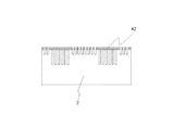
上述の実施の形態1では、光学フィルターの実現のために実効屈折率(nx)が最表面からn1<n2<n3となっていく制御例を示したが、実効的な屈折率の配分がn1<n3<n2となるように3次元構造を作製することでも光学フィルター実現することが可能である。以下、本形態の構造を説明する。図13は、構造をわかりやすくするために、本形態の光学フィルターを分解した斜視図であり、第3層構造体と中層構造体の境界で分離して示している。また、光学フィルターの断面の模式図を図12に示す。
Embodiment 4 FIG.
In the first embodiment described above, an example in which the effective refractive index (n x ) is n 1 <n 2 <n 3 from the outermost surface in order to realize the optical filter has been described. An optical filter can also be realized by producing a three-dimensional structure so that the distribution of n 1 <n 3 <n 2 is satisfied. Hereinafter, the structure of this embodiment will be described. FIG. 13 is an exploded perspective view of the optical filter of the present embodiment for easy understanding of the structure, and is shown separated at the boundary between the third layer structure and the middle layer structure. Moreover, the schematic diagram of the cross section of an optical filter is shown in FIG.
本形態の構造について説明する。下層構造体30は、基板2の表面を加工して中円柱を設けたものである。また、薄いSi基板を中層構造体20とし、さらにそのSi基板の表面を加工して上層小円柱11を形成して上層構造体10としている。中円柱の上面にSi基板(中層構造体20)の底面を接合して3層構造にしたものが本形態の構造である。
The structure of this embodiment will be described. The
この構造により上述の実効屈折率の配分を実現することができる。例えば、図14に示すように、実効屈折率n1=1.5、n2=2.5、n3=2.0(=面積率から制御)及び凹部の深さ(d1=2.0μm,d2=0.6μm,d3=0.7μm)の場合にターゲットとする二つの波長帯で良好な透過特性が得られる。 With this structure, the effective refractive index distribution described above can be realized. For example, as shown in FIG. 14, the effective refractive index n 1 = 1.5, n 2 = 2.5, n 3 = 2.0 (= controlled from the area ratio) and the depth of the recess (d 1 = 2. In the case of 0 μm, d 2 = 0.6 μm, d 3 = 0.7 μm), good transmission characteristics can be obtained in the two target wavelength bands.
上述の形態4において、下層構造体を円柱により形成したが、特に他の形状によって面積率を制御しても問題は無く、角柱、六角形穴、溝でも同様な効果を示す。 In the above-described embodiment 4, the lower layer structure is formed of a cylinder, but there is no problem even if the area ratio is controlled by another shape, and the same effect can be obtained with a prism, hexagonal hole, or groove.
実施の形態5.
上述の実施の形態1では、等価的に3層の光学多層膜となるように3層構造の例を説明した。本実施の形態5では、光学フィルターとしてブロックを周期的に配置した2層構造を説明する。すなわち、下層構造体、上層構造体の2層構造が等価的に2層の光学多層膜となる例を説明する。
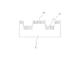
In the first embodiment described above, the example of the three-layer structure has been described so as to be equivalently a three-layer optical multilayer film. In the fifth embodiment, a two-layer structure in which blocks are periodically arranged as an optical filter will be described. That is, an example will be described in which the two-layer structure of the lower layer structure and the upper layer structure is equivalently a two-layer optical multilayer film.
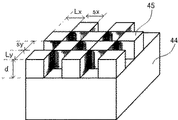
本実施の形態で説明する構造は、第1層内の下層構造体で8〜12μm帯の透過率が大きくなるようにし、第2層内の上層構造体で3〜5μm帯の透過率が大きくなるようにした設計例である。基板44に形成された一層目の下層構造体に相当する大きなブロック45と二層目の上層構造体に相当するそれより小さなブロック46により形成されている。以下、赤外線検出器用の光学フィルターの構成について説明する。
In the structure described in the present embodiment, the transmittance in the 8 to 12 μm band is increased in the lower layer structure in the first layer, and the transmittance in the 3 to 5 μm band is increased in the upper layer structure in the second layer. This is an example of design. A
図15は、本実施の形態の光学設計に係る光学フィルターの下層構造体のみの模式図である。図16は、図15で示したブロックのサイズをパラメータとし、下層構造体のみの光学フィルターの透過率特性の計算結果のグラフである。図17は、係る計算結果から最適のブロックサイズ範囲を検討するために、構造パラメータLと透過率のピーク波長と波長10μmとのずれを表したグラフである。図18は、本実施の形態に係る2層構造の光学フィルターの概略構成を示す斜視図である。図19は、下層構造体のサイズを固定し、上層構造体である第2層目のブロックのサイズをパラメータとして透過率特性を計算した結果のグラフである。図20は、係る計算結果から最適のブロックサイズ範囲を検討するために4μmでの透過率とブロックのサイズの関係を示したグラフである。 FIG. 15 is a schematic view of only the lower layer structure of the optical filter according to the optical design of the present embodiment. FIG. 16 is a graph of the calculation result of the transmittance characteristics of the optical filter of only the lower layer structure using the block size shown in FIG. 15 as a parameter. FIG. 17 is a graph showing the deviation between the structural parameter L, the peak wavelength of the transmittance, and the wavelength of 10 μm in order to examine the optimum block size range from the calculation result. FIG. 18 is a perspective view showing a schematic configuration of an optical filter having a two-layer structure according to the present embodiment. FIG. 19 is a graph showing a result of calculating transmittance characteristics with the size of the lower layer structure fixed and the size of the second layer block as the upper layer structure as a parameter. FIG. 20 is a graph showing the relationship between the transmittance at 4 μm and the block size in order to examine the optimum block size range from the calculation result.
まず、下層構造体の光学設計を説明する。図15に示すような一層目がブロック状のブロック45のみの構造を考える。ここで、ブロック45の縦,横,高さ方向のサイズをLx,Ly,dとし、隣接するブロック45どうしの間隔を縦横それぞれsy,sxとする。また、例えばLxのみ長くするとこの方向の光学的な異方性が生じるので、sx=sy=Lx=Ly=dとして光学異方性がなるべく小さくなるよう光学設計をする。また、構造パラメータLを、L=sx=sy=Lx=Ly=dと定義する。ここで、ブロック45は立方体である。
First, the optical design of the lower layer structure will be described. Consider the structure of only the
構造パラメータLを1μm付近で変化させて透過率を計算した。なお、解析は厳密結合波解析を用いている。また、材質は屈折率3.4のシリコンとした。解析結果のうち代表的な結果を図16に示す。図16を参照すると、8〜12μm付近に透過率の窓(すなわち、透過率の高い領域)が形成され、Lが大きくなるに従い透過率のピークが全体的に長波長側にシフトすることがわかる。 The transmittance was calculated by changing the structural parameter L around 1 μm. The analysis uses exact coupled wave analysis. The material was silicon having a refractive index of 3.4. Representative results of the analysis results are shown in FIG. Referring to FIG. 16, it can be seen that a transmittance window (that is, a region with high transmittance) is formed in the vicinity of 8 to 12 μm, and the transmittance peak is shifted to the longer wavelength side as L is increased. .
下層構造体の光学設計は、8〜12μm帯での吸収率が最大となるように設計することを目的としている。そこで、この帯域に現れるピーク波長と8〜12μm帯の中心波長である波長10μmとのずれに着目し、このずれが最小になる範囲が光学設計として最適な範囲と考え、構造パラメータLを0.9μmから1.7μmまで変化させた場合の透過率を計算した。図17は、構造パラメータLを変化させた場合において、透過率のピーク波長と波長10μmとのずれの変化を表したグラフである。また、このずれ量が小さいほどその構造の透過帯域が8〜12μm帯に入っていることになり、目的とする波長域の赤外光をよく透過させることができる。 The purpose of the optical design of the lower layer structure is to design the absorptance in the 8-12 μm band to be maximum. Therefore, paying attention to the deviation between the peak wavelength appearing in this band and the wavelength of 10 μm, which is the central wavelength of the 8 to 12 μm band, the range where this deviation is minimized is considered the optimum range for optical design, and the structural parameter L is set to 0. The transmittance when changing from 9 μm to 1.7 μm was calculated. FIG. 17 is a graph showing a change in deviation between the peak wavelength of transmittance and the wavelength of 10 μm when the structural parameter L is changed. Further, the smaller the deviation, the more the transmission band of the structure is in the 8 to 12 μm band, and the infrared light in the target wavelength region can be transmitted well.
図17を参照して、下層構造体の8〜12μm帯での透過率のピーク値と波長10μmとのずれ量が2μm以上(図中網掛けの領域)になると設計目標からはずれてしまうので、ずれ量が2μm以下となる1.05μmから1.6μmのLの範囲に設定するのが適当であることがわかる。また、最も効率良く所望の波長域を透過させるのは、Lx=Ly=d=1.3μmであることがわかる。 Referring to FIG. 17, if the amount of deviation between the peak value of the transmittance in the 8 to 12 μm band of the lower layer structure and the wavelength of 10 μm is 2 μm or more (shaded area in the figure), It can be seen that it is appropriate to set the displacement in the L range of 1.05 μm to 1.6 μm where the deviation is 2 μm or less. It can also be seen that Lx = Ly = d = 1.3 μm transmits the desired wavelength region most efficiently.
次に、上層構造体の光学設計を説明する。
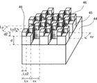
上述のように、下層構造体としてsx=sy=Lx=Ly=d=1.3μmの場合が最適であったので、図15で示した下層構造体のブロック45の上に、上層構造体として更に小さなブロック46を2つ配置した。係る形態が図18である。
Next, the optical design of the upper layer structure will be described.
As described above, since the case of sx = sy = Lx = Ly = d = 1.3 μm was optimal as the lower layer structure, the upper layer structure was formed on the
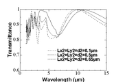
上述した下層構造体の光学設計と同様に、ブロック46の縦,横,高さ方向のサイズをLx2,Ly2,d2とし、L2=Lx2=Ly2=d2として、上層構造体の構造パラメータL2を変化させて計算した。L2の代表的な数値について透過率特性を図19に示す。このようにした2層構造では、8〜12μm付近に加えて新たに3〜5μm帯付近に透過率のピークが現れる。この3〜5μm帯の中心波長である波長4μmにおける透過率をL2に対して表したのが図20である。
Similar to the optical design of the lower layer structure described above, the size of the
図20を参照して、L2=0.4μm以上において透過率が急激に上昇し90%以上となる。よって、上述した2層構造においてはL2=0.4μm以上が望ましいことがわかる。特にLx2=Ly2=d2=0.65μmの場合に、3〜5μm帯付近で透過率が最も高くなっている。つまり、sx=sy=Lx=Ly=d=1.3μm、Lx2=Ly2=d2=0.65μmの2層構造がマルチバンド(3〜5μm帯および8〜12μm帯)の光学フィルターとして最適な構造となる。 Referring to FIG. 20, when L2 = 0.4 μm or more, the transmittance rapidly increases and becomes 90% or more. Therefore, it can be seen that L2 = 0.4 μm or more is desirable in the above-described two-layer structure. In particular, when Lx2 = Ly2 = d2 = 0.65 μm, the transmittance is highest in the vicinity of the 3 to 5 μm band. That is, a two-layer structure of sx = sy = Lx = Ly = d = 1.3 μm and Lx2 = Ly2 = d2 = 0.65 μm is an optimum structure as an optical filter of a multiband (3-5 μm band and 8-12 μm band). It becomes.
上述したように、3辺が等しいブロックでかつブロックどうしの間隔がこのブロックの一辺と等しい長さを備えた条件下で、適宜、光学設計を行えば、目的とする波長帯に透過率のピークを作ることができ、しかも光学的な異方性が生じ難い。 As described above, if the optical design is performed appropriately under the condition that the three sides are equal and the distance between the blocks is equal to the length of one side of the block, the transmittance peak in the target wavelength band. And optical anisotropy hardly occurs.
さらに、3辺が等しいブロックでかつブロックどうしの間隔がこのブロックの一辺と等しい長さを備えた条件の第一層内のブロック群の上に、3辺が等しいブロック群からなる第二層を載せた構成とすることで、2つの波長帯に透過率のピークを持つ光学フィルターを得ることが可能である。 Furthermore, on the block group in the first layer under the condition that the blocks having the same three sides and the interval between the blocks have the same length as one side of the block, the second layer composed of the block groups having the same three sides is provided. By adopting the mounted configuration, it is possible to obtain an optical filter having transmittance peaks in two wavelength bands.
なお、上述した実施の形態においては、上層構造体を構成するブロック群として小さなブロック46を2つ下層構造体を構成するブロック45の上に配置した例を示したが、3辺が等しいブロックであってブロック45の上に配置できるサイズであれば2つ以上配置してもかまわない。この場合でも、適宜、光学設計を行えば目的とする波長帯に透過率のピークを作ることができる。
In the above-described embodiment, the example in which two
このように、ミクロン、サブミクロンスケールのブロックの二層構造を形成することで、それぞれのスケールに対応する異なる波長域を選択的に透過させるようなマルチバンドの光学フィルターの形成が可能である。 In this way, by forming a two-layer structure of micron and submicron scale blocks, it is possible to form a multiband optical filter that selectively transmits different wavelength ranges corresponding to each scale.
実施の形態6.
上述の実施の形態5では、光学フィルターとして3辺が等しいブロックを周期的に配置した2層構造の例を説明した。本実施の形態6では、ブロックの配置数あるいは平面形状を適宜選択することによって、その層内に存在するブロック群の占める比率(すなわち、上述の実施の形態1で定義した面積比率)を操作し透過率の制御が出来ることを説明する。
Embodiment 6 FIG.
In the above-described fifth embodiment, the example of the two-layer structure in which the blocks having the same three sides are periodically arranged as the optical filter has been described. In the sixth embodiment, by appropriately selecting the number of blocks arranged or the planar shape, the ratio of the block group existing in the layer (that is, the area ratio defined in the first embodiment described above) is manipulated. Explain that the transmittance can be controlled.
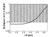
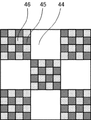
図21は、本実施の形態に係る2層構造の光学フィルターの概略構成を示す斜視図である。図中の点線Aで囲んだ部分を上から見た状態の平面図を図22に示す。図22において、ブロック(ブロック45、ブロック46)の寸法は、上述の実施の形態5で説明した最適の構造であるsx=sy=Lx=Ly=d=1.3μm、Lx2=Ly2=d2=0.65μmである。このサイズを例にして説明する。図22を参照して、第一層目の下層構造体を構成するブロック45の上に第二層目の上層構造体を構成するブロック46が載っている。ここで、第一層目の各ブロック45の上に載っている第二層目のブロック46の個数は2個である。いま、第一層目のブロック45に対して第二層目のブロック46の占有面積を充填率と定義すると、この状態で第一層目のブロック45に対して第二層目のブロック46が占める面積は50%であるので、上記の場合は充填率50%である。
FIG. 21 is a perspective view showing a schematic configuration of an optical filter having a two-layer structure according to the present embodiment. FIG. 22 shows a plan view of the portion surrounded by the dotted line A in the figure as viewed from above. In FIG. 22, the dimensions of the blocks (block 45, block 46) are sx = sy = Lx = Ly = d = 1.3 μm, which is the optimum structure described in the fifth embodiment, and Lx2 = Ly2 = d2 =. 0.65 μm. This size will be described as an example. Referring to FIG. 22, a
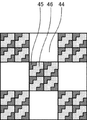
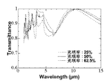
次に、図23に示すように第二層目のブロック46の大きさを図22のブロック46の半分にしたとする。このときの充填率は25%となる。但し、深さ方向(紙面垂直方向)は0.65μmを保つ(以下に示す例でも高さは変えない)。同様に、図24に示すように、図22の状態の第二層目のブロック46の数を増して2倍にすると充填率50%となる。次に、図25に示すように、図23の状態から第二層目のブロック46を変形して占有面積を増やして充填率65%とする。以上の図22〜25のケースのように第二層目のブロック46の充填率を変化させた場合について、透過率を求めた結果が図26に示す透過率特性を示すグラフである。図26を参照すると、充填率に従い特に3〜5μm帯の透過率が大きく変化しているのがわかる。
Next, as shown in FIG. 23, it is assumed that the size of the
上述の各ケースについての3〜5μm帯での極小値(例えば、図26の充填率50%の透過率曲線について波長4μm近辺に示した矢印部分)と充填率との関係を図27に示す。図27から、透過率が約95%以上の高い透過領域に入るのは、充填率が55%から78%の間であることがわかる。 FIG. 27 shows the relationship between the minimum value in the 3 to 5 μm band for each case described above (for example, the arrow portion shown in the vicinity of the wavelength of 4 μm for the transmittance curve of 50% filling rate in FIG. 26) and the filling rate. It can be seen from FIG. 27 that the filling rate is between 55% and 78% when entering the high transmission region where the transmittance is about 95% or more.
上述したように、光学フィルターの基板の主面を平面視して、第一層内のブロックの面積に対する第二層内のブロックの面積の比率を所定の値とすれば、第一層目のブロック群による所定の透過帯域よりも短波長側に第二の透過帯域を作ることができる。したがって、上述した充填率を所定の値とすることによってマルチバンドの光学フィルターを得ることが可能である。 As described above, when the main surface of the substrate of the optical filter is viewed in plan and the ratio of the area of the block in the second layer to the area of the block in the first layer is a predetermined value, the first layer A second transmission band can be formed on a shorter wavelength side than a predetermined transmission band by the block group. Therefore, it is possible to obtain a multiband optical filter by setting the above-described filling rate to a predetermined value.
上述した実施の形態は例示であって、本発明は例示した実施形態の範囲に限定されない。例えば、上述下形態ではフィルター基板の一方の主面に凹凸形状を付加した例を説明したが、フィルター基板の他方の主面にも形成しても良い。本発明は特許請求の範囲によって示され、特許請求の範囲と均等の意味および範囲でのすべての変更が含まれることが意図される。 The above-described embodiment is an exemplification, and the present invention is not limited to the scope of the illustrated embodiment. For example, in the above-described embodiment, the example in which the concavo-convex shape is added to one main surface of the filter substrate has been described, but the filter substrate may be formed on the other main surface of the filter substrate. The present invention is defined by the terms of the claims, and is intended to include any modifications within the scope and meaning equivalent to the terms of the claims.
1 光学フィルター、
2 基板、
3 表面3次元構造体、
4 大円柱
10 上層構造体、
11 上層小円柱、
12 エッチング穴
13 上層基板
20 中層構造体、
30 下層構造体、
31 下層小円柱、
32 エッチング穴
33 エッチング溝
40 フォトレジスト
41 フォトレジスト
42 フォトレジスト
43 フォトレジスト
44 基板
45 1層目のブロック
46 2層目のブロック
1 optical filter,
2 substrates,
3 surface three-dimensional structure,
4
11 Upper small cylinder,
12
30 Underlayer structure,
31 Lower cylinder,
32
Claims (9)
前記基板の主面とこの主面から所定の距離離れた面とで規定される第一層内に、前記光学フィルターが対象とする光を透過し且つ光の波長よりも小さいブロックであって前記距離をその厚みとするブロックからなるブロック群と、
前記第一層に隣接し、前記主面から所定の第二の距離離れた面と前記第一層の表面とで規定される第二層内に、前記第二層の厚みをその厚みとするブロックからなるブロック群と、から構成され、
前記主面を平面視したときのブロック群の占有面積とそれ以外の面積との比率が前記各層内でそれぞれ所定の比率となるように、前記ブロックがそれぞれの層内で配置されたことを特徴とする光学フィルター。 An optical filter substrate;
In the first layer defined by the main surface of the substrate and a surface separated by a predetermined distance from the main surface, the optical filter is a block that transmits light of interest and is smaller than the wavelength of the light, A block group consisting of blocks whose distance is the thickness;
The thickness of the second layer is defined as the thickness of the second layer adjacent to the first layer and defined by the surface separated from the main surface by a predetermined second distance and the surface of the first layer. A block group consisting of blocks,
The blocks are arranged in each layer so that the ratio of the area occupied by the block group when the main surface is viewed in plan and the other area is a predetermined ratio in each layer. An optical filter.
前記主面を平面視して、前記各層内でそれぞれ所定の面積比率でブロックがそれぞれの層内で配置されたことを特徴とする請求項1に記載の光学フィルター。 In a third layer that is adjacent to the second layer and defined by a surface separated from the main surface of the substrate by a third distance and the surface of the second layer, from a block having the thickness of the third layer as its thickness With a block group
2. The optical filter according to claim 1, wherein the main surface is viewed in plan, and blocks are arranged in each layer at a predetermined area ratio in each layer.
前記光学フィルターが対象とする光の波長λよりも小さい開口の穴であって、この基板の主面から所定の深さで掘り込んだ複数の穴を所定の深さ毎に複数群備え、
前記主面を平面視して前記所定の深さ毎に、その深さで複数の前記穴が占有する面積と穴以外の基板の残地の面積との比率がそれぞれ所定の比率となるように前記基板に穴が配設されたことを特徴とする光学フィルター。 On the substrate of the optical filter,
The optical filter is a hole having an opening smaller than the wavelength λ of the target light, and includes a plurality of holes each having a predetermined depth dug from the main surface of the substrate.
The ratio of the area occupied by the plurality of holes at the depth and the area of the remaining area of the substrate other than the holes becomes a predetermined ratio at each predetermined depth when the main surface is viewed in plan. An optical filter, wherein a hole is provided in the substrate.
前記第一層内のブロックに隣接して配置され、前記第一層内のブロックよりも小さい立方体のブロックからなるブロック群を第二層内に有する請求項1に記載の光学フィルター。 A group of blocks that are cubic blocks in the first layer and in which the spacing between adjacent blocks is equal to one side of the cube;
2. The optical filter according to claim 1, wherein the second layer includes a block group that is arranged adjacent to the block in the first layer and includes cubic blocks smaller than the block in the first layer.
前記第一層内のブロックに隣接して配置され、前記第一層内のブロックよりも小さいブロックからなるブロック群を第二層内に有し、
光学フィルターの基板の主面を平面視して、第一層内のブロックの面積に対する第二層内のブロックの面積の比率を所定の値とした請求項1に記載の光学フィルター。 A group of blocks that are cubic blocks in the first layer and in which the distance between adjacent blocks is equal to one side of the cube;
The second layer has a block group that is arranged adjacent to the block in the first layer, and is composed of blocks smaller than the block in the first layer,
The optical filter according to claim 1, wherein the ratio of the area of the block in the second layer to the area of the block in the first layer is set to a predetermined value in plan view of the main surface of the substrate of the optical filter.
Priority Applications (1)
| Application Number | Priority Date | Filing Date | Title |
|---|---|---|---|
| JP2008180898A JP5136249B2 (en) | 2008-07-11 | 2008-07-11 | Optical filter |
Applications Claiming Priority (1)
| Application Number | Priority Date | Filing Date | Title |
|---|---|---|---|
| JP2008180898A JP5136249B2 (en) | 2008-07-11 | 2008-07-11 | Optical filter |
Publications (2)
| Publication Number | Publication Date |
|---|---|
| JP2010020120A true JP2010020120A (en) | 2010-01-28 |
| JP5136249B2 JP5136249B2 (en) | 2013-02-06 |
Family
ID=41705081
Family Applications (1)
| Application Number | Title | Priority Date | Filing Date |
|---|---|---|---|
| JP2008180898A Active JP5136249B2 (en) | 2008-07-11 | 2008-07-11 | Optical filter |
Country Status (1)
| Country | Link |
|---|---|
| JP (1) | JP5136249B2 (en) |
Cited By (3)
| Publication number | Priority date | Publication date | Assignee | Title |
|---|---|---|---|---|
| US8542433B2 (en) | 2011-12-20 | 2013-09-24 | Ngk Insulators, Ltd. | Electromagnetic wave oscillating devices and a method of producing the same |
| US8730565B2 (en) | 2011-03-17 | 2014-05-20 | Ngk Insulators, Ltd. | Electromagnetic wave radiation element and method for producing same |
| US11095835B2 (en) | 2018-12-21 | 2021-08-17 | Imec Vzw | Use of spectral leaks to obtain high spatial resolution information for hyperspectral imaging |
Citations (3)
| Publication number | Priority date | Publication date | Assignee | Title |
|---|---|---|---|---|
| JPH06258512A (en) * | 1993-03-02 | 1994-09-16 | Jasco Corp | Optical filter |
| JP2000171763A (en) * | 1998-12-09 | 2000-06-23 | Nec Corp | Optical transmitter utilizing metallic film having opening part and periodically varying surface form |
| JP2005173120A (en) * | 2003-12-10 | 2005-06-30 | Fuji Photo Film Co Ltd | Low-reflectivity structure and method of manufacturing the same |
-
2008
- 2008-07-11 JP JP2008180898A patent/JP5136249B2/en active Active
Patent Citations (3)
| Publication number | Priority date | Publication date | Assignee | Title |
|---|---|---|---|---|
| JPH06258512A (en) * | 1993-03-02 | 1994-09-16 | Jasco Corp | Optical filter |
| JP2000171763A (en) * | 1998-12-09 | 2000-06-23 | Nec Corp | Optical transmitter utilizing metallic film having opening part and periodically varying surface form |
| JP2005173120A (en) * | 2003-12-10 | 2005-06-30 | Fuji Photo Film Co Ltd | Low-reflectivity structure and method of manufacturing the same |
Cited By (3)
| Publication number | Priority date | Publication date | Assignee | Title |
|---|---|---|---|---|
| US8730565B2 (en) | 2011-03-17 | 2014-05-20 | Ngk Insulators, Ltd. | Electromagnetic wave radiation element and method for producing same |
| US8542433B2 (en) | 2011-12-20 | 2013-09-24 | Ngk Insulators, Ltd. | Electromagnetic wave oscillating devices and a method of producing the same |
| US11095835B2 (en) | 2018-12-21 | 2021-08-17 | Imec Vzw | Use of spectral leaks to obtain high spatial resolution information for hyperspectral imaging |
Also Published As
| Publication number | Publication date |
|---|---|
| JP5136249B2 (en) | 2013-02-06 |
Similar Documents
| Publication | Publication Date | Title |
|---|---|---|
| JP4600577B2 (en) | Diffraction grating element | |
| JP5686227B2 (en) | Wire grid polarizer manufacturing method, nanometer-sized multi-step element, and manufacturing method thereof | |
| US8116002B2 (en) | Grating device with adjusting layer | |
| TWI756459B (en) | Optical elements with multi-level diffractive optical element thin film coating and methods for manufacturing the same | |
| US20140300964A1 (en) | Wire grid polarizer with substrate channels | |
| WO2016016635A1 (en) | Plasmonic filter | |
| KR20130028578A (en) | Photonic crystal structure, method of manufacturing the same, reflective color filter and display apparatus employing the photonic crystal structure | |
| JP2010281876A (en) | Optical element and optical system including the same | |
| JP6292766B2 (en) | Optical filter | |
| KR20230016014A (en) | Gradient encapsulation of waveguide gratings | |
| JP2019035954A5 (en) | ||
| JP5136249B2 (en) | Optical filter | |
| TW202001293A (en) | Metasurface structure and method for producing metasurface structure | |
| CN115421295A (en) | Design method of super lens, super lens and processing technology | |
| JP2016218436A (en) | Diffraction optical element, optical system, and optical instrument | |
| US7420610B2 (en) | Solid-state imaging element, solid-state imaging device, and method for fabricating the same | |
| JP2006267898A (en) | Manufacturing method of three dimensional photonic crystal | |
| JP4914955B2 (en) | ND filter with IR cut function | |
| US20130070343A1 (en) | Fabrication of Micro Lenses | |
| JP6401837B1 (en) | Polarizing plate and optical device | |
| JP2008276074A (en) | Filter for optical communication, and module for optical communication using the same | |
| JP2009237073A (en) | Optical filter | |
| JP2017533451A (en) | Dielectric polarization beam splitter | |
| JP5424730B2 (en) | Manufacturing method of optical filter | |
| JP5136250B2 (en) | Manufacturing method of optical filter |
Legal Events
| Date | Code | Title | Description |
|---|---|---|---|
| A621 | Written request for application examination |
Free format text: JAPANESE INTERMEDIATE CODE: A621 Effective date: 20101006 |
|
| A977 | Report on retrieval |
Free format text: JAPANESE INTERMEDIATE CODE: A971007 Effective date: 20120420 |
|
| A131 | Notification of reasons for refusal |
Free format text: JAPANESE INTERMEDIATE CODE: A131 Effective date: 20120508 |
|
| A521 | Written amendment |
Free format text: JAPANESE INTERMEDIATE CODE: A523 Effective date: 20120628 |
|
| A131 | Notification of reasons for refusal |
Free format text: JAPANESE INTERMEDIATE CODE: A131 Effective date: 20120731 |
|
| A521 | Written amendment |
Free format text: JAPANESE INTERMEDIATE CODE: A523 Effective date: 20120921 |
|
| TRDD | Decision of grant or rejection written | ||
| A01 | Written decision to grant a patent or to grant a registration (utility model) |
Free format text: JAPANESE INTERMEDIATE CODE: A01 Effective date: 20121016 |
|
| A01 | Written decision to grant a patent or to grant a registration (utility model) |
Free format text: JAPANESE INTERMEDIATE CODE: A01 |
|
| A61 | First payment of annual fees (during grant procedure) |
Free format text: JAPANESE INTERMEDIATE CODE: A61 Effective date: 20121029 |
|
| R151 | Written notification of patent or utility model registration |
Ref document number: 5136249 Country of ref document: JP Free format text: JAPANESE INTERMEDIATE CODE: R151 |
|
| FPAY | Renewal fee payment (event date is renewal date of database) |
Free format text: PAYMENT UNTIL: 20151122 Year of fee payment: 3 |
|
| R250 | Receipt of annual fees |
Free format text: JAPANESE INTERMEDIATE CODE: R250 |
|
| R250 | Receipt of annual fees |
Free format text: JAPANESE INTERMEDIATE CODE: R250 |
|
| R250 | Receipt of annual fees |
Free format text: JAPANESE INTERMEDIATE CODE: R250 |
|
| R250 | Receipt of annual fees |
Free format text: JAPANESE INTERMEDIATE CODE: R250 |
|
| R250 | Receipt of annual fees |
Free format text: JAPANESE INTERMEDIATE CODE: R250 |
|
| R250 | Receipt of annual fees |
Free format text: JAPANESE INTERMEDIATE CODE: R250 |
|
| R250 | Receipt of annual fees |
Free format text: JAPANESE INTERMEDIATE CODE: R250 |
|
| R250 | Receipt of annual fees |
Free format text: JAPANESE INTERMEDIATE CODE: R250 |