JP2010016940A - Circuit and method for limiting overcurrent - Google Patents
Circuit and method for limiting overcurrent Download PDFInfo
- Publication number
- JP2010016940A JP2010016940A JP2008173247A JP2008173247A JP2010016940A JP 2010016940 A JP2010016940 A JP 2010016940A JP 2008173247 A JP2008173247 A JP 2008173247A JP 2008173247 A JP2008173247 A JP 2008173247A JP 2010016940 A JP2010016940 A JP 2010016940A
- Authority
- JP
- Japan
- Prior art keywords
- circuit
- power supply
- overcurrent
- current
- coil
- Prior art date
- Legal status (The legal status is an assumption and is not a legal conclusion. Google has not performed a legal analysis and makes no representation as to the accuracy of the status listed.)
- Granted
Links
Images


Landscapes
- Protection Of Static Devices (AREA)
- Rectifiers (AREA)
Abstract
Description
本発明は、供給される交流を直流に変換して出力する電源回路への過電流の流入を制限するための過電流制限回路、および過電流制限方法に関する。 The present invention relates to an overcurrent limiting circuit and an overcurrent limiting method for limiting an inflow of an overcurrent to a power supply circuit that converts a supplied alternating current into a direct current and outputs the converted direct current.
電源装置における電源回路の過電流保護に、簡易、かつ、小型という利点を有するヒューズが一般的に用いられている。交流電源より供給される交流(AC)を直流(DC)に変換して出力する電源回路に対する過電流保護の方法の一例を説明する。 A fuse having an advantage of being simple and small is generally used for overcurrent protection of a power supply circuit in a power supply device. An example of an overcurrent protection method for a power supply circuit that converts alternating current (AC) supplied from an alternating current power source into direct current (DC) and outputs the direct current (DC) will be described.
図3は関連する電源装置の一構成例を示すブロック図である。ここでは、入力過電流保護用ヒューズを用いている。 FIG. 3 is a block diagram illustrating a configuration example of a related power supply apparatus. Here, an input overcurrent protection fuse is used.
図3に示すように、電源装置は、交流電源ACPから供給される電力を直流電圧に変換するスイッチング電源回路50と、交流電圧を直流電圧にするために整流するダイオードブリッジ12とを有する。交流電源ACPは電流経路となる配線61および配線62を介してダイオードブリッジ12と接続され、ダイオードブリッジ12はスイッチング電源回路50と接続されている。
As shown in FIG. 3, the power supply device includes a switching power supply circuit 50 that converts electric power supplied from the AC power supply ACP into a DC voltage, and a
配線61には、交流電源ACPに近い側から、ヒューズ1と、電源装置の起動時に発生する突入電流を温度変化で検出する保護回路2とが順に接続されている。ヒューズ1は、入力過電流保護回路として機能するため、保護回路2よりも交流電源ACPに近い側に設けられている。また、保護回路2と並列にリレー3が設けられている。 From the side close to the AC power supply ACP, the fuse 1 and the protection circuit 2 that detects an inrush current generated at the time of starting the power supply device by temperature change are connected to the wiring 61 in order. Since the fuse 1 functions as an input overcurrent protection circuit, the fuse 1 is provided closer to the AC power supply ACP than the protection circuit 2. A relay 3 is provided in parallel with the protection circuit 2.
保護回路2は、温度ヒューズ21および抵抗22を有する。抵抗22に突入電流が一定時間以上流れると、抵抗22の温度が上昇し、温度ヒューズ21が抵抗22の温度で溶断する。 The protection circuit 2 includes a thermal fuse 21 and a resistor 22. When an inrush current flows through the resistor 22 for a predetermined time or more, the temperature of the resistor 22 rises and the temperature fuse 21 is blown at the temperature of the resistor 22.
リレー3は、スイッチ31と、磁力によりスイッチ31を動作させるコイル32とを有する。コイル32の両端に定電圧Vccが印加されると、コイル32に電流が流れ、コイル32に発生する磁場によりスイッチ31が閉じる。なお、定電圧Vccは、スイッチング電源回路50から供給されるものであってもよく、図に示さない電源回路から供給されるものであってもよい。 The relay 3 includes a switch 31 and a coil 32 that operates the switch 31 by magnetic force. When a constant voltage Vcc is applied across the coil 32, a current flows through the coil 32, and the switch 31 is closed by a magnetic field generated in the coil 32. The constant voltage Vcc may be supplied from the switching power supply circuit 50, or may be supplied from a power supply circuit not shown in the drawing.
スイッチング電源回路50は、ダイオードブリッジ12から出力される電圧を平滑する平滑コンデンサ13、トランス14、電源制御IC15、電流検出抵抗16、スイッチング素子17、ダイオード18、および平滑コンデンサ19を有する。DC電圧出力の短絡による過電流に対して、次のようにして、電源制御IC15による過電流保護制御で電源回路が保護される。電源制御IC15は、DC電圧出力の電流上昇を電流検出抵抗16の両端で電圧上昇として検出し、電流検出抵抗16の両端の電圧が予め設定された基準電圧を超えていると、DC電圧出力が過電流状態であることを認識し、スイッチング素子17をオフにする。
The switching power supply circuit 50 includes a smoothing capacitor 13 that smoothes a voltage output from the
次に、図3に示した電源装置における、DC電圧出力以外の過電流に対する保護方法を説明する。 Next, a method for protecting against overcurrent other than DC voltage output in the power supply device shown in FIG. 3 will be described.
図3に示す電源装置の起動時には、交流電源ACPから配線61を通る電流はヒューズ1および保護回路2を経由してダイオードブリッジ12に到達する。所定の時間経過後、リレー3に定電圧Vccが印加されるとスイッチ31がオンになり、配線61を通る電流はヒューズ1およびリレー3を経由してダイオードブリッジ12に流れるようになる。
When the power supply device shown in FIG. 3 is started, the current passing through the wiring 61 from the AC power supply ACP reaches the
このようにして、電源装置の起動時に発生しやすい突入電流に対して、スイッチング電源回路50はヒューズ1および保護回路2により保護される。電源装置が立ち上がり、DC電圧の出力が安定すると、交流電流はバイパス回路となるリレー3を経由してダイオードブリッジ12に流れ込み、DC電圧出力以外の過電流に対して、スイッチング電源回路50はヒューズ1を用いた入力過電流保護回路により保護される。
In this way, the switching power supply circuit 50 is protected by the fuse 1 and the protection circuit 2 against an inrush current that is likely to occur when the power supply device is started. When the power supply device starts up and the output of the DC voltage is stabilized, the alternating current flows into the
なお、突入電流を電源装置の二次側で制限するための別の方法が特許文献1に開示されている。
上記ヒューズ1は、通常、電源内部の平滑コンデンサ13に流入する突入電流に対しての溶断特性で決められるため、実際に使用する定常電流値に対して数倍の電流容量のヒューズが選定される。そのため、ヒューズ自体の溶断特性よりその定格電流の2倍程度の電流を流しても長時間溶断しない特性となっている。 Since the fuse 1 is usually determined by the fusing characteristics with respect to the inrush current flowing into the smoothing capacitor 13 inside the power supply, a fuse having a current capacity several times that of the actual current value to be actually used is selected. . For this reason, the fuse itself does not blow for a long time even when a current about twice its rated current is passed.
電源装置が安定動作し、リレー3がバイパス回路として機能している状態で、DC出力以外の箇所による過電流があることも考えられる。この場合、保護回路2も電源制御IC15による制御も機能しないので、保護素子であるヒューズ1がその過電流により溶断されなければならないが、上述の特性によりヒューズ1はすぐには溶断せず、溶断するまでに電源回路内の基板パターンや部品に過電流がダメージを与えてしまうおそれがある。
In a state where the power supply device operates stably and the relay 3 functions as a bypass circuit, there may be an overcurrent due to a location other than the DC output. In this case, since the protection circuit 2 and the control by the power
本発明は上述したような技術が有する問題点を解決するためになされたものであり、突入電流だけでなく、それ以外の過電流からも電源回路を保護することを可能にした過電流制限回路および過電流保護方法を提供することを目的とする。 The present invention has been made to solve the above-described problems of the technology, and an overcurrent limiting circuit that can protect a power supply circuit from not only an inrush current but also an overcurrent other than that. And an overcurrent protection method.
上記目的を達成するための本発明の過電流制限回路は、
交流電源と該交流電源から供給される交流を直流に変換して出力する電源回路とを接続する電流経路に設けられ、前記電源回路への過電流の流入を制限する保護回路と、
前記電流経路に前記保護回路と並列に設けられたバイパス回路と、
前記バイパス回路を非導通状態に予め設定し、前記交流電源による交流供給開始から所定の時間経過後に前記バイパス回路を導通状態に切り替え、前記交流電源から出力される電流を監視し、過電流を検出すると、前記バイパス回路を非導通状態に切り替える検出回路と、
を有する構成である。
In order to achieve the above object, the overcurrent limiting circuit of the present invention comprises:
A protection circuit for limiting an inflow of overcurrent to the power supply circuit, provided in a current path connecting an AC power supply and a power supply circuit that converts the alternating current supplied from the alternating current power supply into a direct current and outputs the direct current;
A bypass circuit provided in parallel with the protection circuit in the current path;
The bypass circuit is set in a non-conducting state in advance, the bypass circuit is switched to a conducting state after a predetermined time has elapsed from the start of AC supply by the AC power source, the current output from the AC power source is monitored, and an overcurrent is detected Then, a detection circuit that switches the bypass circuit to a non-conductive state;
It is the structure which has.
また、本発明の過電流制限方法は、交流電源と該交流電源から供給される交流を直流に変換して出力する電源回路との間に設けられ、前記電源回路への過電流の流入を制限する保護回路を用いた、前記電源回路に対する過電流制限方法であって、
前記保護回路に並列に配置されたバイパス回路を非導通状態に予め設定し、
前記交流電源による前記交流供給開始から所定の時間経過後に前記バイパス回路を導通状態に切り替え、
前記交流電源から出力される電流を監視し、過電流を検出すると、前記バイパス回路を非導通状態に切り替えるものである。
Further, the overcurrent limiting method of the present invention is provided between an AC power supply and a power supply circuit that converts the AC supplied from the AC power supply into a DC and outputs it, and limits the inflow of overcurrent to the power supply circuit. An overcurrent limiting method for the power supply circuit using a protection circuit that includes:
Presetting the bypass circuit arranged in parallel with the protection circuit in a non-conductive state;
The bypass circuit is switched to a conductive state after a predetermined time has elapsed from the start of the AC supply by the AC power source,
The current output from the AC power supply is monitored, and when the overcurrent is detected, the bypass circuit is switched to a non-conductive state.
本発明によれば、電源回路の起動時に発生する突入電流以外の過電流が発生しても、保護回路で電源回路への過電流を遮断することができる。 According to the present invention, even if an overcurrent other than an inrush current generated at the time of starting the power supply circuit occurs, the overcurrent to the power supply circuit can be blocked by the protection circuit.
本発明の過電流制限回路の実施形態を説明する。 An embodiment of the overcurrent limiting circuit of the present invention will be described.
本実施形態の過電流制限回路を用いた電源装置の構成を説明する。以下では、図3に示した構成と同様な構成については同一の符号を付し、その詳細な説明を省略する。 A configuration of a power supply device using the overcurrent limiting circuit of the present embodiment will be described. In the following, the same components as those shown in FIG. 3 are denoted by the same reference numerals, and detailed description thereof is omitted.
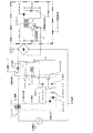
図1は本実施形態の電源装置の一構成例を示すブロック図である。図1に示す電源装置は、過電流を検出してリレー3を制御する検出回路70が図3に示した構成に追加されている。本実施形態の過電流制限回路は、保護回路2、リレー3および検出回路70を有する構成である。 FIG. 1 is a block diagram illustrating a configuration example of the power supply device according to the present embodiment. In the power supply device shown in FIG. 1, a detection circuit 70 that detects an overcurrent and controls the relay 3 is added to the configuration shown in FIG. The overcurrent limiting circuit according to the present embodiment has a configuration including a protection circuit 2, a relay 3, and a detection circuit 70.
検出回路70は、過電流を検出するためのコイル7と、検出された電流を整流するダイオード8,9と、平滑コンデンサ10と、コイル7が過電流を検出するとオンするトランジスタ11と、リレー3のスイッチ31の開閉を制御するトランジスタ4と、トランジスタ4のベース電極に印加する電圧を設定するための抵抗5,6とを有する構成である。 The detection circuit 70 includes a coil 7 for detecting an overcurrent, diodes 8 and 9 for rectifying the detected current, a smoothing capacitor 10, a transistor 11 that is turned on when the coil 7 detects an overcurrent, and a relay 3 The transistor 4 controls the opening and closing of the switch 31 and resistors 5 and 6 for setting the voltage applied to the base electrode of the transistor 4.
コイル7の一方の端子が配線63を介してトランジスタ11のベース電極に接続され、コイル7の他方の端子が配線64を介してトランジスタ11のエミッタ電極に接続されている。ダイオード8は、配線63の途中に設けられ、アノード端子がコイル7に接続され、カソード端子がトランジスタ11のベース電極に接続されている。ダイオード9は、アノード端子が配線64に接続され、カソード端子がトランジスタ11のベース電極に接続されている。平滑コンデンサ10は、一方の端子がトランジスタ11のベース電極に接続され、他方の端子が接地されている。 One terminal of the coil 7 is connected to the base electrode of the transistor 11 through the wiring 63, and the other terminal of the coil 7 is connected to the emitter electrode of the transistor 11 through the wiring 64. The diode 8 is provided in the middle of the wiring 63, the anode terminal is connected to the coil 7, and the cathode terminal is connected to the base electrode of the transistor 11. The diode 9 has an anode terminal connected to the wiring 64 and a cathode terminal connected to the base electrode of the transistor 11. The smoothing capacitor 10 has one terminal connected to the base electrode of the transistor 11 and the other terminal grounded.
コイル7が配線61に流れる交流電流を検出すると、誘導起電力によって交流電圧が発生し、その交流電圧がダイオード8,9および平滑コンデンサ10により平滑され、平滑された電圧がトランジスタ11のベース電極に印加される。コイル7に生じる起電力は、コイル7が正常な交流電流を検出したときよりも過電流を検出したときの方が大きい。 When the coil 7 detects an alternating current flowing through the wiring 61, an alternating voltage is generated by the induced electromotive force, and the alternating voltage is smoothed by the diodes 8 and 9 and the smoothing capacitor 10, and the smoothed voltage is applied to the base electrode of the transistor 11. Applied. The electromotive force generated in the coil 7 is greater when an overcurrent is detected than when the coil 7 detects a normal alternating current.
トランジスタ11は、コレクタ電極が抵抗5と抵抗6の間に接続され、エミッタ電極が接地されている。トランジスタ11は、正常な交流電流による起電力による電圧がベース電極に印加されても、オフのままであるが、コイル7が過電流を検出して生じる起電力による電圧がベース電極に印加されるとオンになる。 The transistor 11 has a collector electrode connected between the resistors 5 and 6 and an emitter electrode grounded. The transistor 11 remains off even when a voltage due to an electromotive force due to a normal alternating current is applied to the base electrode, but a voltage due to the electromotive force generated when the coil 7 detects an overcurrent is applied to the base electrode. And turn on.
トランジスタ4は、ベース電極が抵抗5と抵抗6の間に接続され、コレクタ電極がリレー3のコイル32の一方の端子と接続され、エミッタ電極が接地されている。トランジスタ4は、定電圧Vccが抵抗5,6により分圧された電圧がベース電極に印加されることで、オン状態を維持する。また、トランジスタ11がオンすることでトランジスタ4のベース電極に印加される電圧が閾値電圧より低くなると、トランジスタ4はオフする。トランジスタ4がオフすると、リレー3のコイル32に電流が流れなくなる。 The transistor 4 has a base electrode connected between the resistors 5 and 6, a collector electrode connected to one terminal of the coil 32 of the relay 3, and an emitter electrode grounded. The transistor 4 is kept on by applying a voltage obtained by dividing the constant voltage Vcc by the resistors 5 and 6 to the base electrode. Further, when the transistor 11 is turned on and the voltage applied to the base electrode of the transistor 4 becomes lower than the threshold voltage, the transistor 4 is turned off. When the transistor 4 is turned off, no current flows through the coil 32 of the relay 3.
ここで、電源装置の起動時に発生する突入電流を保護回路2で制限するための時間を考える。その時間は、本来、発生した突入電流が減衰してスイッチング電源回路50への影響が無視できるほど小さくなるまでの時間に設定されるのが理想的である。しかし、全ての突入電流の減衰時間を把握するのは困難である。そこで、スイッチング電源回路50が直流電圧を出力可能になれば、突入電流による影響はなくなっているものと仮定する。この仮定により本実施形態では、上記時間を、交流電源ACPによる交流供給開始からトランジスタ4に直流電圧が印加されるまでの時間とするが、この場合に限らない。また、スイッチング電源回路50以外の直流電圧出力回路(不図示)から直流電圧が抵抗5,6に供給されてもよい。 Here, a time for limiting the inrush current generated when the power supply device is started up by the protection circuit 2 will be considered. The time is ideally set to a time until the generated inrush current is attenuated and the influence on the switching power supply circuit 50 becomes negligible. However, it is difficult to grasp the decay time of all inrush currents. Therefore, it is assumed that if the switching power supply circuit 50 can output a DC voltage, the influence of the inrush current is eliminated. According to this assumption, in the present embodiment, the above time is the time from the start of AC supply by the AC power supply ACP until the DC voltage is applied to the transistor 4, but this is not a limitation. Further, a DC voltage may be supplied to the resistors 5 and 6 from a DC voltage output circuit (not shown) other than the switching power supply circuit 50.
なお、トランジスタ4の閾値電圧、トランジスタ11の閾値電圧、および抵抗5,6のそれぞれの抵抗値は、正常な交流電流が配線61に流れるときにコイル7に生じる起電力による電圧と、過電流が配線61に流れたときにコイル7に生じる起電力の電圧とに基づいて設定される。 Note that the threshold voltage of the transistor 4, the threshold voltage of the transistor 11, and the resistance values of the resistors 5 and 6 are the voltage caused by the electromotive force generated in the coil 7 when a normal alternating current flows through the wiring 61, and the overcurrent. It is set based on the voltage of the electromotive force generated in the coil 7 when it flows through the wiring 61.
保護回路2は、図3で説明したように、突入電流により抵抗22が発熱し、温度ヒューズ21が溶断してスイッチング電源回路50への突入電流の流れ込みを制限する突入電流制限回路として機能する。本実施形態では、上記突入電流の場合に限らず、過電流が入力されると、突入電流の場合と同様にスイッチング電源回路50への過電流の流れ込みを制限する。このことから、保護回路2は、過電流保護回路として機能する。 As described with reference to FIG. 3, the protection circuit 2 functions as an inrush current limiting circuit that restricts the inrush current flowing into the switching power supply circuit 50 when the resistor 22 generates heat due to the inrush current and the temperature fuse 21 is melted. In the present embodiment, not only in the case of the inrush current, when an overcurrent is input, the flow of the overcurrent to the switching power supply circuit 50 is restricted as in the case of the inrush current. For this reason, the protection circuit 2 functions as an overcurrent protection circuit.
図2は交流電流検出用のコイルの一構成例を示す外観模式図である。図2に示す回路基板65に検出回路70を設けているが、この図ではコイル7以外の構成を図に示すことを省略している。 FIG. 2 is a schematic external view showing a configuration example of a coil for detecting an alternating current. Although the detection circuit 70 is provided on the circuit board 65 shown in FIG. 2, the illustration of the configuration other than the coil 7 is omitted in this figure.
検出回路70のコイル7は、図2に示すように、回路基板65に2次元の配線パターンで形成されている。配線61は回路基板65の表側からコイル7の中心を通って回路基板65の裏側に抜けるように設けられている。この構成により、図2の左側の交流電源(不図示)から配線61を介して流れ出た交流電流は、コイル7の中心を通って回路基板65の表側から裏側に抜ける。なお、回路基板65には、検出回路70の他に、スイッチング電源回路50など他の構成が設けられていてもよい。 As shown in FIG. 2, the coil 7 of the detection circuit 70 is formed on the circuit board 65 with a two-dimensional wiring pattern. The wiring 61 is provided so as to pass through the center of the coil 7 from the front side of the circuit board 65 to the back side of the circuit board 65. With this configuration, the alternating current that flows out from the AC power source (not shown) on the left side of FIG. 2 through the wiring 61 passes through the center of the coil 7 and flows from the front side to the back side of the circuit board 65. In addition to the detection circuit 70, the circuit board 65 may be provided with other configurations such as the switching power supply circuit 50.
次に、図1に示した電源装置の動作を説明する。ここでは、電源装置の立ち上げ後に過電流が発生した場合とする。 Next, the operation of the power supply device shown in FIG. 1 will be described. Here, it is assumed that an overcurrent occurs after the power supply device is started up.
電源装置を起動した後、スイッチング電源回路50が直流電圧の出力を開始すると、トランジスタ4のベース電極に閾値電圧以上の電圧が印加され、トランジスタ4がオンになる。トランジスタ4がオンすることで、リレー3のスイッチ31がオンして、リレー3が導通状態になる。 When the switching power supply circuit 50 starts outputting a DC voltage after starting the power supply device, a voltage equal to or higher than the threshold voltage is applied to the base electrode of the transistor 4 and the transistor 4 is turned on. When the transistor 4 is turned on, the switch 31 of the relay 3 is turned on, and the relay 3 becomes conductive.
コイル7が配線61に流れる交流電流を検出し、コイル7に生じる誘導起電力による交流電圧がダイオード8,9および平滑コンデンサ10により平滑され、平滑された電圧がトランジスタ11のベース電極に印加される。印加される電圧はトランジスタ11の閾値電圧に達していないため、トランジスタ11はオンしない。そのため、トランジスタ4はオン状態を維持し、リレー3は導通状態のままである。 The coil 7 detects an alternating current flowing through the wiring 61, an alternating voltage due to the induced electromotive force generated in the coil 7 is smoothed by the diodes 8 and 9 and the smoothing capacitor 10, and the smoothed voltage is applied to the base electrode of the transistor 11. . Since the applied voltage does not reach the threshold voltage of the transistor 11, the transistor 11 is not turned on. Therefore, the transistor 4 remains on, and the relay 3 remains conductive.
ここで、配線61に過電流が流れると、コイル7が過電流を検出し、コイル7に生じる起電力が正常な交流電流のときよりも大きくなる。トランジスタ11のベース電極に、過電流によってコイル7に生じる起電力による電圧が印加されると、その電圧が閾値電圧以上であるため、トランジスタ11はオンする。 Here, when an overcurrent flows through the wiring 61, the coil 7 detects the overcurrent, and the electromotive force generated in the coil 7 becomes larger than that in a normal alternating current. When a voltage due to an electromotive force generated in the coil 7 due to an overcurrent is applied to the base electrode of the transistor 11, the transistor 11 is turned on because the voltage is equal to or higher than the threshold voltage.
トランジスタ11がオンすると、トランジスタ4のベース電極に印加される電圧が閾値電圧より低くなり、トランジスタ4はオフする。トランジスタ4がオフすると、リレー3のコイル32に電流が流れなくなり、スイッチ31がオフする。スイッチ31がオフすると、リレー3が非導通状態になり、配線61の電流経路が保護回路2のみを経由する経路に切り替わる。 When the transistor 11 is turned on, the voltage applied to the base electrode of the transistor 4 becomes lower than the threshold voltage, and the transistor 4 is turned off. When the transistor 4 is turned off, no current flows through the coil 32 of the relay 3, and the switch 31 is turned off. When the switch 31 is turned off, the relay 3 is turned off, and the current path of the wiring 61 is switched to a path that passes only through the protection circuit 2.
上記電流経路の切り替えにより、過電流が保護回路2の抵抗22を流れるようになると、抵抗22が発熱し、温度ヒューズ21がその熱により溶断し、交流電源ACPからスイッチング電源回路50への電力供給が遮断される。 When overcurrent flows through the resistor 22 of the protection circuit 2 due to the switching of the current path, the resistor 22 generates heat, the thermal fuse 21 is blown by the heat, and power is supplied from the AC power supply ACP to the switching power supply circuit 50. Is cut off.
本実施形態によれば、スイッチング電源回路のDC電圧出力以外での異常による過電流が発生すると、バイパス回路が非導通状態になり、電流経路が保護回路のみを経由する経路に切り替わる。そのため、保護回路に内蔵された温度ヒューズが抵抗の温度上昇を検知し、設定された温度で温度ヒューズが溶断する。その結果、交流電流のスイッチング電源回路への入力が遮断され、過電流がスイッチング電源回路に流れ込むことが制限される。これにより、スイッチング電源回路の基板パターンや部品に過電流がダメージを与えることを防止できる。 According to the present embodiment, when an overcurrent due to an abnormality other than the DC voltage output of the switching power supply circuit occurs, the bypass circuit becomes non-conductive, and the current path is switched to a path that passes only through the protection circuit. Therefore, the temperature fuse built in the protection circuit detects the temperature rise of the resistor, and the temperature fuse is blown at the set temperature. As a result, the input of alternating current to the switching power supply circuit is cut off, and the overcurrent is restricted from flowing into the switching power supply circuit. Thereby, it is possible to prevent the overcurrent from damaging the substrate pattern and components of the switching power supply circuit.
また、交流電源からの交流電流の入力直近に簡易的なパターンで交流電流検出用のコイル7を設けることにより、スイッチング電源回路の広範囲に異常を発生させる前に、電流供給源に近いところで過電流が検出される。そして、突入電流制限回路を過電流保護回路として兼用することで、簡素、かつ、低価格で過電流制限回路を作製することができる。 In addition, by providing an alternating current detection coil 7 with a simple pattern in the immediate vicinity of the alternating current input from the alternating current power supply, an overcurrent is generated near the current supply source before an abnormality occurs in a wide range of the switching power supply circuit. Is detected. By using the inrush current limiting circuit also as the overcurrent protection circuit, the overcurrent limiting circuit can be manufactured simply and at a low cost.
本発明によれば、起動時に発生する突入電流以外の過電流が発生しても、保護回路で電源回路への過電流を遮断することができる。 According to the present invention, even if an overcurrent other than the inrush current generated at the time of start-up occurs, the overcurrent to the power supply circuit can be interrupted by the protection circuit.
なお、上述した実施形態において、バイポーラトランジスタの代わりにMOSトランジスタを用いてもよい。 In the embodiment described above, a MOS transistor may be used instead of the bipolar transistor.
1 ヒューズ
2 保護回路
3 リレー
4,11 トランジスタ
5,6 抵抗
7 コイル
8,9 ダイオード
10,13,19 平滑コンデンサ
12 ダイオードブリッジ
14 トランス
15 電源制御IC
16 電流検出抵抗
17 スイッチング素子
18 ダイオード
DESCRIPTION OF SYMBOLS 1 Fuse 2 Protection circuit 3 Relay 4,11 Transistor 5,6 Resistance 7 Coil 8,9 Diode 10,13,19
16
Claims (6)
前記電流経路に前記保護回路と並列に設けられたバイパス回路と、
前記バイパス回路を非導通状態に予め設定し、前記交流電源による交流供給開始から所定の時間経過後に前記バイパス回路を導通状態に切り替え、前記交流電源から出力される電流を監視し、過電流を検出すると、前記バイパス回路を非導通状態に切り替える検出回路と、
を有する過電流制限回路。 A protection circuit for limiting an inflow of overcurrent to the power supply circuit, provided in a current path connecting an AC power supply and a power supply circuit that converts alternating current supplied from the alternating current power supply into direct current and outputs;
A bypass circuit provided in parallel with the protection circuit in the current path;
The bypass circuit is set in a non-conductive state in advance, the bypass circuit is switched to a conductive state after a predetermined time has elapsed since the start of AC supply by the AC power source, the current output from the AC power source is monitored, and an overcurrent is detected Then, a detection circuit that switches the bypass circuit to a non-conductive state;
An overcurrent limiting circuit.
前記電流を検出するコイルと、該コイルが前記過電流を検出しない場合、前記バイパス回路を導通状態に維持し、前記コイルが前記過電流を検出する場合、前記バイパス回路を非導通状態にするトランジスタと、を有する請求項1記載の過電流制限回路。 The detection circuit includes:
A coil for detecting the current, and a transistor for maintaining the bypass circuit in a conductive state when the coil does not detect the overcurrent, and for disabling the bypass circuit when the coil detects the overcurrent The overcurrent limiting circuit according to claim 1.
前記過電流の入力により発熱する抵抗と、該抵抗の発熱により所定の温度以上になると溶断する温度ヒューズと、を有する請求項1から4のいずれか1項記載の過電流制限回路。 The protection circuit is
5. The overcurrent limiting circuit according to claim 1, further comprising: a resistor that generates heat when the overcurrent is input; and a thermal fuse that blows when a temperature rises above a predetermined temperature due to heat generated by the resistor.
前記保護回路に並列に配置されたバイパス回路を非導通状態に予め設定し、
前記交流電源による前記交流供給開始から所定の時間経過後に前記バイパス回路を導通状態に切り替え、
前記交流電源から出力される電流を監視し、過電流を検出すると、前記バイパス回路を非導通状態に切り替える、過電流制限方法。 For the power supply circuit using a protection circuit that is provided between an AC power supply and a power supply circuit that converts the alternating current supplied from the alternating current power supply into a direct current and outputs the direct current, and restricts the inflow of overcurrent to the power supply circuit. An overcurrent limiting method,
Presetting the bypass circuit arranged in parallel with the protection circuit in a non-conductive state;
The bypass circuit is switched to a conductive state after a predetermined time has elapsed from the start of the AC supply by the AC power source,
An overcurrent limiting method for monitoring a current output from the AC power supply and switching the bypass circuit to a non-conduction state when an overcurrent is detected.
Priority Applications (1)
| Application Number | Priority Date | Filing Date | Title |
|---|---|---|---|
| JP2008173247A JP5450988B2 (en) | 2008-07-02 | 2008-07-02 | Overcurrent limiting circuit |
Applications Claiming Priority (1)
| Application Number | Priority Date | Filing Date | Title |
|---|---|---|---|
| JP2008173247A JP5450988B2 (en) | 2008-07-02 | 2008-07-02 | Overcurrent limiting circuit |
Publications (2)
| Publication Number | Publication Date |
|---|---|
| JP2010016940A true JP2010016940A (en) | 2010-01-21 |
| JP5450988B2 JP5450988B2 (en) | 2014-03-26 |
Family
ID=41702483
Family Applications (1)
| Application Number | Title | Priority Date | Filing Date |
|---|---|---|---|
| JP2008173247A Active JP5450988B2 (en) | 2008-07-02 | 2008-07-02 | Overcurrent limiting circuit |
Country Status (1)
| Country | Link |
|---|---|
| JP (1) | JP5450988B2 (en) |
Citations (5)
| Publication number | Priority date | Publication date | Assignee | Title |
|---|---|---|---|---|
| JPH04200276A (en) * | 1990-11-29 | 1992-07-21 | Sony Corp | Power supply device |
| JP2005204378A (en) * | 2004-01-14 | 2005-07-28 | Matsushita Electric Ind Co Ltd | Power supply circuit |
| JP2007225406A (en) * | 2006-02-23 | 2007-09-06 | Matsushita Electric Works Ltd | Ac current detection coil |
| JP2007267473A (en) * | 2006-03-28 | 2007-10-11 | Matsushita Electric Ind Co Ltd | Inrush current prevention circuit |
| JP2008109779A (en) * | 2006-10-25 | 2008-05-08 | Sharp Corp | Device for preventing overcurrent |
-
2008
- 2008-07-02 JP JP2008173247A patent/JP5450988B2/en active Active
Patent Citations (5)
| Publication number | Priority date | Publication date | Assignee | Title |
|---|---|---|---|---|
| JPH04200276A (en) * | 1990-11-29 | 1992-07-21 | Sony Corp | Power supply device |
| JP2005204378A (en) * | 2004-01-14 | 2005-07-28 | Matsushita Electric Ind Co Ltd | Power supply circuit |
| JP2007225406A (en) * | 2006-02-23 | 2007-09-06 | Matsushita Electric Works Ltd | Ac current detection coil |
| JP2007267473A (en) * | 2006-03-28 | 2007-10-11 | Matsushita Electric Ind Co Ltd | Inrush current prevention circuit |
| JP2008109779A (en) * | 2006-10-25 | 2008-05-08 | Sharp Corp | Device for preventing overcurrent |
Also Published As
| Publication number | Publication date |
|---|---|
| JP5450988B2 (en) | 2014-03-26 |
Similar Documents
| Publication | Publication Date | Title |
|---|---|---|
| EP2804278B1 (en) | Self-power circuit for protecting relay | |
| JP2007043822A (en) | Overvoltage protection circuit | |
| JP4983523B2 (en) | Power supply circuit and earth leakage circuit breaker using the power supply circuit | |
| CN113557646A (en) | Method and device for protecting an electrical load | |
| US9270106B2 (en) | Temperature protection device of electronic device | |
| JP2008228538A (en) | Switching power supply unit | |
| JP5768741B2 (en) | Earth leakage breaker | |
| US6355912B2 (en) | Safety circuit for heating devices using PTC wire | |
| US11486600B2 (en) | Air conditioner | |
| JP5126241B2 (en) | Overvoltage protection circuit and overvoltage protection method | |
| JPH11149320A (en) | Protection means for power circuit | |
| JP2008295254A (en) | Lightning arrester | |
| JP2005323489A (en) | Protective circuit | |
| JP5450988B2 (en) | Overcurrent limiting circuit | |
| JP2002186174A (en) | Protection circuit for power supply circuit | |
| JP2009081901A (en) | Device for preventing excessive voltage | |
| JPH11289657A (en) | Rush current deterring unit | |
| JP4623560B2 (en) | Earth leakage breaker | |
| JP2004015961A (en) | Ground fault interrupter with three-phase phase-failure protector | |
| JP4716412B2 (en) | DC power supply overcurrent protection circuit | |
| JP2006006070A (en) | Load protecting device | |
| JP6776652B2 (en) | Relay control device and earth leakage safety device | |
| JP2002204566A (en) | Rush current preventing circuit for direct-current power circuit | |
| CN115882421B (en) | Electronic fuse circuit and circuit system using same | |
| JP3775251B2 (en) | Multi-output power supply circuit and multi-output power supply method |
Legal Events
| Date | Code | Title | Description |
|---|---|---|---|
| A621 | Written request for application examination |
Free format text: JAPANESE INTERMEDIATE CODE: A621 Effective date: 20100921 |
|
| A131 | Notification of reasons for refusal |
Free format text: JAPANESE INTERMEDIATE CODE: A131 Effective date: 20120424 |
|
| A977 | Report on retrieval |
Free format text: JAPANESE INTERMEDIATE CODE: A971007 Effective date: 20120425 |
|
| A521 | Written amendment |
Free format text: JAPANESE INTERMEDIATE CODE: A523 Effective date: 20120625 |
|
| A131 | Notification of reasons for refusal |
Free format text: JAPANESE INTERMEDIATE CODE: A131 Effective date: 20121016 |
|
| A131 | Notification of reasons for refusal |
Free format text: JAPANESE INTERMEDIATE CODE: A131 Effective date: 20130618 |
|
| A521 | Written amendment |
Free format text: JAPANESE INTERMEDIATE CODE: A523 Effective date: 20130814 |
|
| TRDD | Decision of grant or rejection written | ||
| A01 | Written decision to grant a patent or to grant a registration (utility model) |
Free format text: JAPANESE INTERMEDIATE CODE: A01 Effective date: 20131203 |
|
| A61 | First payment of annual fees (during grant procedure) |
Free format text: JAPANESE INTERMEDIATE CODE: A61 Effective date: 20131226 |
|
| R150 | Certificate of patent or registration of utility model |
Ref document number: 5450988 Country of ref document: JP Free format text: JAPANESE INTERMEDIATE CODE: R150 Free format text: JAPANESE INTERMEDIATE CODE: R150 |
|
| S533 | Written request for registration of change of name |
Free format text: JAPANESE INTERMEDIATE CODE: R313533 |
|
| R350 | Written notification of registration of transfer |
Free format text: JAPANESE INTERMEDIATE CODE: R350 |