JP2010016704A - Array antenna - Google Patents
Array antenna Download PDFInfo
- Publication number
- JP2010016704A JP2010016704A JP2008175931A JP2008175931A JP2010016704A JP 2010016704 A JP2010016704 A JP 2010016704A JP 2008175931 A JP2008175931 A JP 2008175931A JP 2008175931 A JP2008175931 A JP 2008175931A JP 2010016704 A JP2010016704 A JP 2010016704A
- Authority
- JP
- Japan
- Prior art keywords
- radiating element
- array antenna
- radiation
- pairs
- amplitude
- Prior art date
- Legal status (The legal status is an assumption and is not a legal conclusion. Google has not performed a legal analysis and makes no representation as to the accuracy of the status listed.)
- Granted
Links
Images


Landscapes
- Variable-Direction Aerials And Aerial Arrays (AREA)
- Waveguide Aerials (AREA)
Abstract
Description
この発明は、複数の放射素子と給電点とを結ぶ給電回路内で多重反射波が発生するアレーアンテナに関する。 The present invention relates to an array antenna in which multiple reflected waves are generated in a feed circuit connecting a plurality of radiating elements and a feed point.
一般的なアレーアンテナとして、各放射素子に対して、所望の励振振幅・位相(以下、励振分布という)で給電して所望の放射特性を実現するものには、移相器又は増幅器を直結接続して振幅・位相を制御するフェーズドアレー形式がある。しかしながら、この形式の場合、構成が全体的に複雑で高コストとなるため、固定ビームを与えるアンテナとして用いられることは少ない。 As a general array antenna, a phase shifter or an amplifier is directly connected to each radiating element to achieve the desired radiation characteristics by supplying power with the desired excitation amplitude and phase (hereinafter referred to as excitation distribution). There is a phased array type that controls the amplitude and phase. However, in the case of this type, since the configuration is generally complicated and expensive, it is rarely used as an antenna that gives a fixed beam.
これに対して、固定ビームを実現するアンテナ構成の一例として、マイクロストリップアレーアンテナが知られている。このマイクロストリップアレーアンテナにおいて、放射素子と同一平面上に給電回路を構成する共平面給電方式では、一度のエッチングで加工ができ、製造が容易で低コスト化が図れる。これに加えて、薄型化、軽量化も容易である。 On the other hand, a microstrip array antenna is known as an example of an antenna configuration that realizes a fixed beam. In this microstrip array antenna, the coplanar power feeding system in which the power feeding circuit is configured on the same plane as the radiating element can be processed by one etching, and can be easily manufactured and reduced in cost. In addition to this, it is easy to reduce the thickness and weight.
また、マイクロストリップアレーアンテナにおいて、給電点から入力された電波は、マイクロストリップ線路により構成されるT分岐線路などにより所望の励振分布で放射素子に給電される。このT分岐線路は、比較的コンパクトな寸法で構成することができるため、共平面給電方式のマイクロストリップアレーアンテナの給電回路では一般的な電力合成・分配回路としてよく使用されている(例えば、特許文献1,2参照)。
In the microstrip array antenna, the radio wave input from the feeding point is fed to the radiating element with a desired excitation distribution by a T-branch line constituted by a microstrip line. Since this T-branch line can be configured with a relatively compact size, it is often used as a general power combining / distribution circuit in a feeding circuit of a coplanar feeding type microstrip array antenna (for example, a patent)
ここで、一般的にマイクロストリップアレーアンテナには、T分岐線路が分配器として用いられるが、このT分岐線路には、アイソレーションがないため、内部を通過する電波が反射されたり、放射素子で反射されてT字分配器に戻る電波がT分岐線路で再反射されたりして、多重反射波が生じる。 Here, in general, a T-branch line is used as a distributor in a microstrip array antenna. However, since this T-branch line has no isolation, a radio wave passing therethrough is reflected or a radiating element is used. The radio wave reflected and returned to the T-shaped distributor is re-reflected by the T-branch line, and multiple reflected waves are generated.
この結果、多重反射波に起因して放射素子の放射特性に誤差が生じ、所望の放射特性から大きく外れてしまう。つまり、入力端子側から見た場合のインピーダンスの整合がとれていても、出力端子側から見た場合のインピーダンスの整合がとれていない状態となってしまう。このため、アレーアンテナの電磁界分布、即ち励振分布に乱れが生じ、放射素子の所望の放射特性が得られないという問題があった。 As a result, an error occurs in the radiation characteristic of the radiating element due to the multiple reflected waves, which greatly deviates from the desired radiation characteristic. In other words, even if impedance matching when viewed from the input terminal side is achieved, impedance matching when viewed from the output terminal side is not achieved. For this reason, the electromagnetic field distribution, that is, the excitation distribution of the array antenna is disturbed, and there is a problem that desired radiation characteristics of the radiation element cannot be obtained.
なお、例えば、内部にアイソレーションが設けられたウィルキンソン分配器等の電力合成・分配回路を用いることによって、多重反射波の発生を抑えることが可能となる。しかしながら、このような電力合成・分配回路を用いた構成を採用した場合、アレーアンテナ自体のサイズが大型化してしまうため、マイクロストリップアレーアンテナには、不向きであった。この他に、放射素子及び給電回路を互いに異なる基板に実装する多層給電方式がある。しかしながら、このような構成を採用した場合にも、アレーアンテナ自体のサイズが大型化したり、製造コストが高くなったりするという問題が生じてしまう。 For example, the use of a power combining / distribution circuit such as a Wilkinson distributor with isolation provided therein can suppress the generation of multiple reflected waves. However, when such a configuration using a power combining / distribution circuit is adopted, the size of the array antenna itself is increased, which is not suitable for a microstrip array antenna. In addition to this, there is a multilayer feeding system in which the radiating element and the feeding circuit are mounted on different substrates. However, even when such a configuration is adopted, there arises a problem that the size of the array antenna itself is increased and the manufacturing cost is increased.
この発明は、上記のような課題を解決するためになされたものであり、アイソレーションを省略し多重反射波の発生を許容する給電構造において、所定の空間領域又は角度方向における励振分布の乱れを最小限に抑えることができるアレーアンテナを得ることを目的とする。 The present invention has been made to solve the above-described problems, and in a feed structure that allows the generation of multiple reflected waves by omitting isolation, disturbance of the excitation distribution in a predetermined spatial region or angular direction is prevented. An object is to obtain an array antenna that can be minimized.
この発明に係るアレーアンテナは、給電回路内の多重反射波による誤差によって所望の放射特性の振幅よりも小さな振幅で放射する第1放射素子と、多重反射波による誤差によって所望の放射特性の振幅よりも大きな振幅で放射する第2放射素子とにより構成され、第1放射素子及び第2放射素子が給電回路内の同一分岐点を経て給電される放射素子対を複数配置したものであって、複数の放射素子対は、所定の観測面へ向けて投影される第1放射素子及び第2放射素子の多重反射波による誤差同士が互いに相殺されるように配置されているものである。 The array antenna according to the present invention includes a first radiating element that radiates at an amplitude smaller than an amplitude of a desired radiation characteristic due to an error due to multiple reflected waves in the feed circuit, and an amplitude of the desired radiation characteristic due to an error due to multiple reflected waves. And a plurality of radiation element pairs in which the first radiation element and the second radiation element are fed through the same branch point in the power feeding circuit. The radiating element pairs are arranged so that errors due to multiple reflected waves of the first radiating element and the second radiating element projected toward a predetermined observation surface are canceled out from each other.
この発明のアレーアンテナによれば、所定の観測面へ向けて投影される第1放射素子及び第2放射素子の誤差同士が互いに相殺されるように、複数の放射素子対が配置されているので、アイソレーションを省略し多重反射波による誤差の発生を許容する給電構造において、所定の空間領域又は角度方向における励振分布の乱れを最小限に抑えることができる。 According to the array antenna of the present invention, the plurality of pairs of radiating elements are arranged so that the errors of the first radiating element and the second radiating element projected toward a predetermined observation surface are canceled out from each other. In a feed structure that eliminates isolation and allows errors due to multiple reflected waves, disturbance of the excitation distribution in a predetermined spatial region or angular direction can be minimized.
以下、この発明を実施するための最良の形態について、図面を参照して説明する。
実施の形態1.
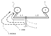
図1は、この発明の実施の形態1によるマイクロストリップアレーアンテナを示す構成図である。なお、図1の矢示Aは、第1の方向であり、方位角(AZ:Azimuth)を示す。また、矢示Bは、第1の方向に対して直交する第2の方向であり、仰角(EL:Elevation)を示す。線Cは、第1の方向Aに沿う所定の観測面としての第1観測面(観測線)を示す。この所定の観測面とは、多重反射波による誤差の影響を抑制したい観測面である。線Dは、第2の方向Bに沿う第2観測面(観測線)を示す。線Eは、給電回路の中心点を通り、かつ第1観測面Cに対して平行な基準線である。これらの矢示A,B及び線C,D,Eについては、他の図でも同様である。
The best mode for carrying out the present invention will be described below with reference to the drawings.
1 is a block diagram showing a microstrip array antenna according to
図1において、共平面形のアンテナ用基板は、地導体、誘電体基板、及びストリップ導体によって構成されている。地導体は、誘電体基板の一方の面に配置されている。ストリップ導体は、誘電体基板の他方の面に配置されている。アンテナ用基板には、給電点1、及び複数の放射素子対(素子ペア)2が設けられている。
In FIG. 1, a coplanar antenna substrate is constituted by a ground conductor, a dielectric substrate, and a strip conductor. The ground conductor is disposed on one surface of the dielectric substrate. The strip conductor is disposed on the other surface of the dielectric substrate. The antenna substrate is provided with a
また、アンテナ用基板のストリップ導体は、マイクロストリップ線路3及び複数のT分岐線路4(分配器)を形成している。なお、T分岐線路4については、図中破線で示す。マイクロストリップ線路3及び複数のT分岐線路4によって、給電点1から複数の放射素子対2への電力の伝送経路、即ち給電回路が構成されている。複数の放射素子対2は、それぞれ第1放射素子5及び第2放射素子6によって構成されている。なお、所望の放射特性を得るために(必要な励振分布を実現するために)、各箇所のマイクロストリップ線路3の長さや、T分岐線路4の分配比あるいは形状・種類等が選定される。
The strip conductor of the antenna substrate forms a
次に、第1放射素子5及び第2放射素子6の放射特性について具体的に説明する。図2は、図1の第1及び第2放射素子5,6の多重反射モデルの一例を説明するための説明図である。図2において、T分岐線路4と第1放射素子5との間の距離L1は、T分岐線路4と第2放射素子6との間の距離L2よりも短くなっている(L1≠L2)。
Next, the radiation characteristics of the first
このような線路構成において、T分岐線路4からの入射波Fの一部が第1放射素子5で反射されて、反射波となってT分岐線路4に戻る。その反射波がT分岐線路(分配器)4で再び反射されて第1素子5へ戻り、再反射波Gが生じる。なお、再反射波Gの他にも、例えば、入射波Fが第1放射素子5で反射された電波となって第2放射素子6へ伝わり、第2放射素子6で再び反射されるような再反射波、あるいはT分岐線路4から第2放射素子に進行した入射波Fが第2放射素子6で反射されて第1放射素子5に入射する反射波(図示せず)も生じる。
In such a line configuration, a part of the incident wave F from the
第1放射素子5への入射波Fの位相と再反射波Gの位相とは、互いに異なる。これにより、入射波Fが再反射波G等による多重反射波によって減衰(干渉)され、第1放射素子5の放射特性の振幅が、所望の放射特性の振幅よりも小さくなる(マイナスの誤差が生じる)。一方、第2放射素子6では、入射波が再反射波等による多重反射波によって増幅(合成)され、第2放射素子6の放射特性の振幅が、所望の放射特性の振幅よりも大きくなる(プラスの誤差が生じる)。
The phase of the incident wave F to the first
ここで、先の図1において、複数の放射素子対2は、第1の方向A及び第2の方向Bにそれぞれ沿って並べられている。また、複数の放射素子対2のそれぞれの第1放射素子5及び第2放射素子6は、第2の方向Bで互いに隣り合うように配置されている。さらに、複数の放射素子対2の第1放射素子5同士は、第1の方向Aで互いに隣り合うように配置されている。これと同様に、複数の放射素子対2の第2放射素子6同士は、第1の方向Aで互いに隣り合うように配置されている。
Here, in FIG. 1, the plurality of
また、複数の放射素子対2の第2放射素子は、基準線E側に配置されている。即ち、複数の放射素子対2は、基準線Eに対して線対称になるように並べられている。このような複数の放射素子対2の配列によって、第1観測面Cへ向けて投影される第1放射素子5及び第2放射素子6の放射特性に含まれる誤差の分布が図1の(a)に示すようになる。また、第2観測面Dへ向けた第1放射素子5及び第2放射素子6の放射特性に含まれる誤差の分布が図1の(b)に示すようになる。
Further, the second radiating elements of the plurality of
従って、図1の(a)に示すように、第1放射素子5の放射特性に含まれるマイナスの誤差と、第2放射素子6の放射特性に含まれるプラスの誤差とが互いに相殺され、放射素子対2の第1観測面Cでの放射特性における振幅は、所望の放射特性の振幅となる。つまり、複数の放射素子対2は、第1観測面Cへ向けて投影される第1放射素子5及び第2放射素子6の多重反射波による誤差同士が互いに相殺されるように配置されている。
Accordingly, as shown in FIG. 1A, the negative error included in the radiation characteristic of the first
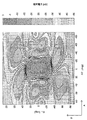
ここで、図3は、多重反射波による誤差の影響を考慮せずに放射素子対2を並べた場合のマイクロストリップアレーアンテナの放射パターンを示す特性図である(従来のものの特性図)。図4は、図1のマイクロストリップアレーアンテナの放射パターンを示す特性図である。図5は、多重反射波による誤差の影響が無い場合の理想状態でのマイクロストリップアレーアンテナの放射パターンを示す特性図である。なお、各特性図の中心領域(AZ=0,EL=0の周辺の領域)は、マイクロストリップアレーアンテナから放射されたメインビームを示す。
Here, FIG. 3 is a characteristic diagram showing a radiation pattern of the microstrip array antenna when the
多重反射波による誤差の影響を考慮していない場合の放射パターンでは、図3に示すように、メインビーム以外の領域において、励振分布の乱れが生じており、マイクロストリップアレーアンテナからサイドローブが、ほぼ不規則に放射されていることが解る。これに対して、図1のマイクロストリップアレーアンテナの放射パターンは、図4に示すように、第1の方向Aにおいて、誤差のない理想状態での放射パターンである図5とほぼ同じ放射パターンとなっていることが解る。即ち、図1のマイクロストリップアレーアンテナでは、所望の観測面において誤差の影響による励振分布の乱れを最小限に抑えることができ、多重反射波による励振分布の乱れが抑制されている。 In the radiation pattern in the case where the influence of the error due to the multiple reflected waves is not considered, as shown in FIG. 3, the excitation distribution is disturbed in the region other than the main beam, and the side lobe is generated from the microstrip array antenna. It can be seen that the radiation is almost irregular. On the other hand, the radiation pattern of the microstrip array antenna of FIG. 1 is substantially the same as that of FIG. 5 which is a radiation pattern in an ideal state with no error in the first direction A, as shown in FIG. I understand that it is. That is, in the microstrip array antenna of FIG. 1, the disturbance of the excitation distribution due to the influence of errors can be minimized on the desired observation plane, and the disturbance of the excitation distribution due to multiple reflected waves is suppressed.
上記のようなマイクロストリップアレーアンテナでは、複数の放射素子対2が、第1観測面Cへ向けて投影される第1放射素子5及び第2放射素子6の多重反射波による誤差同士が互いに相殺されるように配置されている。この構成により、アイソレーションを省略し多重反射波の発生を許容する給電構造において、所定の空間領域又は角度方向における励振分布の乱れを最小限に抑えることができる。
In the microstrip array antenna as described above, errors due to the multiple reflected waves of the
実施の形態2.
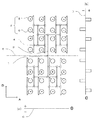
実施の形態1では、先の図1に示すように、基準線E側に第2放射素子6が配置されていた。これに対して、実施の形態2では、図6に示すように、基準線E側に第1放射素子5が配置されている。即ち、実施の形態2では、放射素子対2における第1放射素子5と第2放射素子6との配列が逆になっている。他の構成は、実施の形態1と同様である。
In the first embodiment, as shown in FIG. 1, the
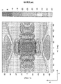
ここで、先の図1に示すマイクロストリップアレーアンテナの放射パターンと、図6に示すマイクロストリップアレーアンテナの放射パターンとを比較する。図7は、図6のマイクロストリップアレーアンテナの放射パターンを示す特性図である。まず、先の図4の特性図においては、図5の特性図における誤差がない場合に比べて、第2の方向Bに対するメインビーム幅は若干拡大するものの、サイドローブレベルはほとんど上昇していない。これに対して、図7の特性図においては、第2の方向Bに対するサイドローブレベルは上昇するものの、メインビーム幅の拡大は抑えられる。 Here, the radiation pattern of the microstrip array antenna shown in FIG. 1 is compared with the radiation pattern of the microstrip array antenna shown in FIG. FIG. 7 is a characteristic diagram showing a radiation pattern of the microstrip array antenna of FIG. First, in the characteristic diagram of FIG. 4, the side beam level hardly increases although the main beam width in the second direction B is slightly increased as compared with the case where there is no error in the characteristic diagram of FIG. . On the other hand, in the characteristic diagram of FIG. 7, although the side lobe level in the second direction B increases, the expansion of the main beam width can be suppressed.
従って、マイクロストリップアレーアンテナの特性において、サイドローブレベルの抑制とメインビーム幅の収束性とのうち、サイドローブレベルの抑制を優先する場合には、実施の形態1の構成(図1の構成)を用いればよい。これに対して、メインビーム幅の収束性を優先する場合には、実施の形態2の構成(図6の構成)を用いればよい。 Therefore, in the characteristics of the microstrip array antenna, when priority is given to the suppression of the side lobe level among the suppression of the side lobe level and the convergence of the main beam width, the configuration of the first embodiment (configuration of FIG. 1). May be used. On the other hand, when priority is given to the convergence of the main beam width, the configuration of the second embodiment (configuration of FIG. 6) may be used.
実施の形態3.
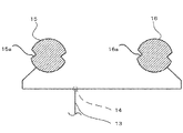
実施の形態3では、具体的なペア素子の構成例として、第1放射素子15及び第2放射素子16が1点給電方式の円偏波放射用の放射素子である場合について説明する。
In the third embodiment, a case where the
図8は、この発明の実施の形態3によるマイクロストリップアレーアンテナの一部を示す構成図である。図8において、実施の形態3の第1放射素子15及び第2放射素子16は、マイクロストリップ線路13及びT分岐線路14を介して給電点から給電される。また、第1放射素子15及び第2放射素子16は、1点給電方式の円偏波放射用の放射素子である。さらに、第1放射素子15及び第2放射素子16には、それぞれ円偏波励振用切り欠き15a,16aが設けられている。
FIG. 8 is a block diagram showing a part of a microstrip array antenna according to
また、第1放射素子15の向きは、第2放射素子16の向きに対して、第1の方向又は第2の方向へ90度ずらして(回転して)配置されている。T分岐線路14は、第1放射素子15と第2放射素子16との位相差が90度となるようになっている。他の構成は実施の形態1又は実施の形態2と同様である。
Further, the direction of the
上記のようなマイクロストリップアレーアンテナでは、第1放射素子15及び第2放射素子16の素子端からの反射波の位相がT分岐線路14で同相とはならないことにより多重反射波が生じる。この多重反射波の影響による励振分布の乱れについても、実施の形態1、2と同様に、その構造を変更することなく最小限に抑えることができる。
In the microstrip array antenna as described above, multiple reflected waves are generated because the phases of the reflected waves from the element ends of the
実施の形態4.
実施の形態3では、第1放射素子15及び第2放射素子16が、1点給電方式の円偏波放射用の放射素子であった。これに対して、実施の形態4では、第1放射素子25及び第2放射素子26が、2点給電方式の円偏波放射用の放射素子である。
In the third embodiment, the
図9は、この発明の実施の形態4によるマイクロストリップアレーアンテナの一部を示す構成図である。図9において、実施の形態4の第1放射素子25及び第2放射素子26は、マイクロストリップ線路23及びT分岐線路24a,24b,24cを介して給電点から給電される。他の構成は、実施の形態3と同様である。
FIG. 9 is a block diagram showing a part of a microstrip array antenna according to
上記のようなマイクロストリップアレーアンテナでは、第1放射素子25及び第2放射素子26が2点給電方式の円偏波放射用の放射素子である場合であっても、実施の形態3と同様の効果を得ることができる。
In the microstrip array antenna as described above, even when the
なお、実施の形態1,2では、第1観測面Cを所定の観測面としたが、第2観測面を所定の観測面としてもよい。つまり、第1の方向Aを、仰角とし、第2の方向Bを方位角としてもよい。 In the first and second embodiments, the first observation plane C is a predetermined observation plane, but the second observation plane may be a predetermined observation plane. That is, the first direction A may be an elevation angle and the second direction B may be an azimuth angle.
また、実施の形態1〜4では、マイクロストリップアレーアンテナについて説明したが、この発明は、マイクロストリップアレーアンテナ以外のアレーアンテナにも適用することができる。 In the first to fourth embodiments, the microstrip array antenna has been described. However, the present invention can also be applied to array antennas other than the microstrip array antenna.
さらに、実施の形態1〜4では、放射素子の数が32個の場合について説明した。しかしながら、放射素子の数は、この例に限るものではなく、励振分布の誤差量が+と−との対となる2素子ペアの配列を基本として、所望の観測面へ向けて投影した誤差が相殺できるよう2のべき乗個であれば、任意の数でよい。 Further, in the first to fourth embodiments, the case where the number of radiating elements is 32 has been described. However, the number of radiating elements is not limited to this example, and an error projected onto a desired observation plane is based on an array of two element pairs in which the amount of error in the excitation distribution is a pair of + and −. Any number may be used as long as it is a power of 2 so that it can be offset.
1 給電点、2 放射素子対、4,14,24a,24b,24c T分岐線路(分岐点)、5,15,25 第1放射素子、6,16,26 第2放射素子、C 第1観測面(所定の観測面)、D 第2観測面、E 基準線。
DESCRIPTION OF
Claims (6)
前記複数の放射素子対は、所定の観測面へ向けて投影される前記第1放射素子及び前記第2放射素子の前記多重反射波による誤差同士が互いに相殺されるように配置されている
ことを特徴とするアレーアンテナ。 A first radiating element that radiates with an amplitude smaller than the amplitude of the desired radiation characteristic due to an error due to multiple reflected waves in the power supply circuit, and radiates with an amplitude larger than the amplitude of the desired radiation characteristic due to the error due to the multiple reflected waves An array antenna including a plurality of radiating element pairs, each of which is configured by a second radiating element, and wherein the first radiating element and the second radiating element are fed through the same branch point in the feeding circuit,
The plurality of radiating element pairs are arranged such that errors due to the multiple reflected waves of the first radiating element and the second radiating element projected toward a predetermined observation surface cancel each other. Characteristic array antenna.
ことを特徴とする請求項1記載のアレーアンテナ。 The array antenna according to claim 1, wherein the plurality of radiating element pairs are arranged along a direction orthogonal to the observation surface.
前記複数の放射素子対は、前記基準線に対して線対称になるように並べられている
ことを特徴とする請求項2記載のアレーアンテナ。 The second radiating element of the plurality of radiating element pairs is disposed on a reference line side passing through a central point of the feeder circuit and parallel to the observation plane;
The array antenna according to claim 2, wherein the plurality of radiating element pairs are arranged in line symmetry with respect to the reference line.
前記複数の放射素子対は、前記基準線に対して線対称になるように並べられている
ことを特徴とする請求項2記載のアレーアンテナ。 The first radiating element of the plurality of radiating element pairs is disposed on a reference line side passing through a center point of the feeder circuit and parallel to the observation surface,
The array antenna according to claim 2, wherein the plurality of radiating element pairs are arranged in line symmetry with respect to the reference line.
ことを特徴とする請求項1から請求項4までのいずれか1項に記載のアレーアンテナ。 The array antenna according to any one of claims 1 to 4, wherein each of the first radiating element and the second radiating element is a radiating element for circularly polarized radiation.
前記複数の放射素子対の前記第1放射素子及び前記第2放射素子は、前記給電回路の前記同一分岐点からの励振電圧の位相差が90度となるように設定されている
ことを特徴とする請求項5記載のアレーアンテナ。 The direction of the first radiating element of the plurality of radiating element pairs is arranged to be shifted by 90 degrees with respect to the direction of the second radiating element,
The first radiating element and the second radiating element of the plurality of radiating element pairs are set so that a phase difference of an excitation voltage from the same branch point of the feeder circuit is 90 degrees. The array antenna according to claim 5.
Priority Applications (1)
| Application Number | Priority Date | Filing Date | Title |
|---|---|---|---|
| JP2008175931A JP5089509B2 (en) | 2008-07-04 | 2008-07-04 | Array antenna |
Applications Claiming Priority (1)
| Application Number | Priority Date | Filing Date | Title |
|---|---|---|---|
| JP2008175931A JP5089509B2 (en) | 2008-07-04 | 2008-07-04 | Array antenna |
Publications (2)
| Publication Number | Publication Date |
|---|---|
| JP2010016704A true JP2010016704A (en) | 2010-01-21 |
| JP5089509B2 JP5089509B2 (en) | 2012-12-05 |
Family
ID=41702362
Family Applications (1)
| Application Number | Title | Priority Date | Filing Date |
|---|---|---|---|
| JP2008175931A Expired - Fee Related JP5089509B2 (en) | 2008-07-04 | 2008-07-04 | Array antenna |
Country Status (1)
| Country | Link |
|---|---|
| JP (1) | JP5089509B2 (en) |
Cited By (1)
| Publication number | Priority date | Publication date | Assignee | Title |
|---|---|---|---|---|
| CN111987480A (en) * | 2020-08-17 | 2020-11-24 | 中国科学院国家空间科学中心 | Reflective array antenna and design method thereof |
Citations (4)
| Publication number | Priority date | Publication date | Assignee | Title |
|---|---|---|---|---|
| JPS6126303U (en) * | 1984-07-24 | 1986-02-17 | 八木アンテナ株式会社 | SHF planar antenna |
| JP2000082920A (en) * | 1998-09-04 | 2000-03-21 | Mitsubishi Electric Corp | Micro strip array antenna |
| JP2002043837A (en) * | 2000-06-29 | 2002-02-08 | Thomson Licensing Sa | Transmitter/receiver for electromagnetic waves fed from array manufactured by microstrip technique |
| JP2003347842A (en) * | 2002-05-24 | 2003-12-05 | Hitachi Cable Ltd | Array antenna device |
-
2008
- 2008-07-04 JP JP2008175931A patent/JP5089509B2/en not_active Expired - Fee Related
Patent Citations (4)
| Publication number | Priority date | Publication date | Assignee | Title |
|---|---|---|---|---|
| JPS6126303U (en) * | 1984-07-24 | 1986-02-17 | 八木アンテナ株式会社 | SHF planar antenna |
| JP2000082920A (en) * | 1998-09-04 | 2000-03-21 | Mitsubishi Electric Corp | Micro strip array antenna |
| JP2002043837A (en) * | 2000-06-29 | 2002-02-08 | Thomson Licensing Sa | Transmitter/receiver for electromagnetic waves fed from array manufactured by microstrip technique |
| JP2003347842A (en) * | 2002-05-24 | 2003-12-05 | Hitachi Cable Ltd | Array antenna device |
Cited By (2)
| Publication number | Priority date | Publication date | Assignee | Title |
|---|---|---|---|---|
| CN111987480A (en) * | 2020-08-17 | 2020-11-24 | 中国科学院国家空间科学中心 | Reflective array antenna and design method thereof |
| CN111987480B (en) * | 2020-08-17 | 2023-03-24 | 中国科学院国家空间科学中心 | Reflective array antenna and design method thereof |
Also Published As
| Publication number | Publication date |
|---|---|
| JP5089509B2 (en) | 2012-12-05 |
Similar Documents
| Publication | Publication Date | Title |
|---|---|---|
| JP7077587B2 (en) | Dual band patch antenna | |
| JP6807707B2 (en) | Antenna device | |
| JP4602276B2 (en) | Waveguide slot array antenna device | |
| US8860612B2 (en) | Antenna device for generating reconfigurable high-order mode conical beam | |
| JP6988278B2 (en) | Array antenna | |
| JP2019009544A (en) | Dual band patch antenna | |
| JP2017046107A (en) | Antenna device | |
| WO2017085871A1 (en) | Power feed circuit and antenna device | |
| JP4772715B2 (en) | Antenna device | |
| JP5089509B2 (en) | Array antenna | |
| JP7292800B2 (en) | Planar array antenna for both transmission and reception | |
| JP6409676B2 (en) | Array antenna and antenna for satellite communication | |
| WO2015129089A1 (en) | Array antenna device | |
| JP5918874B1 (en) | Array antenna | |
| CN104882681A (en) | Circularly polarized antenna and manufacture method thereof | |
| JP2019012970A (en) | Transmission/reception shared planar antenna element and transmission/reception shared planar array antenna | |
| WO2018198970A1 (en) | Antenna device | |
| US10680307B2 (en) | Waveguide to strip line transducer including a waveguide wall forming substrate having an end surface bonded to a second conductor, and a power feed circuit formed therefrom | |
| JP2001267835A (en) | Circularly polarized wave microstrip antenna and cross polarization component reducing method to be used for the antenna | |
| JP4591425B2 (en) | Antenna device | |
| JP2008042375A (en) | Strip line feed circuit and triplate type plane sector beam antenna provided with the feed circuit | |
| JP2002223120A (en) | Circularly polarized wave type planar array antenna | |
| JP2017175282A (en) | Reception antenna device | |
| JP6022129B1 (en) | Feed circuit and antenna device | |
| WO2020053935A1 (en) | Antenna device |
Legal Events
| Date | Code | Title | Description |
|---|---|---|---|
| A621 | Written request for application examination |
Free format text: JAPANESE INTERMEDIATE CODE: A621 Effective date: 20110428 |
|
| A977 | Report on retrieval |
Free format text: JAPANESE INTERMEDIATE CODE: A971007 Effective date: 20120222 |
|
| A131 | Notification of reasons for refusal |
Free format text: JAPANESE INTERMEDIATE CODE: A131 Effective date: 20120228 |
|
| A521 | Request for written amendment filed |
Free format text: JAPANESE INTERMEDIATE CODE: A523 Effective date: 20120329 |
|
| A131 | Notification of reasons for refusal |
Free format text: JAPANESE INTERMEDIATE CODE: A131 Effective date: 20120529 |
|
| A521 | Request for written amendment filed |
Free format text: JAPANESE INTERMEDIATE CODE: A523 Effective date: 20120719 |
|
| TRDD | Decision of grant or rejection written | ||
| A01 | Written decision to grant a patent or to grant a registration (utility model) |
Free format text: JAPANESE INTERMEDIATE CODE: A01 Effective date: 20120814 |
|
| A01 | Written decision to grant a patent or to grant a registration (utility model) |
Free format text: JAPANESE INTERMEDIATE CODE: A01 |
|
| A61 | First payment of annual fees (during grant procedure) |
Free format text: JAPANESE INTERMEDIATE CODE: A61 Effective date: 20120911 |
|
| FPAY | Renewal fee payment (event date is renewal date of database) |
Free format text: PAYMENT UNTIL: 20150921 Year of fee payment: 3 |
|
| R150 | Certificate of patent or registration of utility model |
Ref document number: 5089509 Country of ref document: JP Free format text: JAPANESE INTERMEDIATE CODE: R150 Free format text: JAPANESE INTERMEDIATE CODE: R150 |
|
| R250 | Receipt of annual fees |
Free format text: JAPANESE INTERMEDIATE CODE: R250 |
|
| R250 | Receipt of annual fees |
Free format text: JAPANESE INTERMEDIATE CODE: R250 |
|
| R250 | Receipt of annual fees |
Free format text: JAPANESE INTERMEDIATE CODE: R250 |
|
| R250 | Receipt of annual fees |
Free format text: JAPANESE INTERMEDIATE CODE: R250 |
|
| R250 | Receipt of annual fees |
Free format text: JAPANESE INTERMEDIATE CODE: R250 |
|
| R250 | Receipt of annual fees |
Free format text: JAPANESE INTERMEDIATE CODE: R250 |
|
| LAPS | Cancellation because of no payment of annual fees |