JP2010009351A - Memory controller, memory system and control method for memory device - Google Patents
Memory controller, memory system and control method for memory device Download PDFInfo
- Publication number
- JP2010009351A JP2010009351A JP2008168467A JP2008168467A JP2010009351A JP 2010009351 A JP2010009351 A JP 2010009351A JP 2008168467 A JP2008168467 A JP 2008168467A JP 2008168467 A JP2008168467 A JP 2008168467A JP 2010009351 A JP2010009351 A JP 2010009351A
- Authority
- JP
- Japan
- Prior art keywords
- data
- output
- input
- memory
- memory device
- Prior art date
- Legal status (The legal status is an assumption and is not a legal conclusion. Google has not performed a legal analysis and makes no representation as to the accuracy of the status listed.)
- Granted
Links
Images


Abstract
Description
本発明はメモリ制御装置、メモリシステムおよびメモリ装置の制御方法に関し、ストローブ信号を用いメモリ装置とのデータの入出力タイミングを制御するメモリ制御装置、メモリシステムおよびメモリ装置の制御方法に関する。 The present invention relates to a memory control device, a memory system, and a memory device control method, and more particularly to a memory control device, a memory system, and a memory device control method for controlling data input / output timing with a memory device using a strobe signal.
ダブル・データ・レート(DDR)タイプのメモリ装置とのデータ線上のデータの入出力は、クロック周期の1/2の周期で行う。このため、高速なデータの入出力が可能である。このようなメモリ装置においては、データストローブ線を配置し、データを入出力するタイミングの通知にデータストローブ信号を用いる。高速にデータ入出力を行う場合、データの確定誤差精度を向上させるため、データストローブ信号は差動信号である。一対差動ストローブ信号のクロスポイントが入出力データの取り込み基準点となる。最初のデータを入出力するための差動ストローブ信号のクロスポイントを作成するため、データを入出力前にデータストローブ線上にプリアンブル期間を設けている(特許文献1参照)。
しかしながら、メモリ制御装置が2つのメモリ装置間とそれぞれデータ入出力する場合、2つのメモリ装置が、データの入出力のためのそれぞれのプリアンブル期間とデータ入出力が重なると、バスファイトしてしまう。また、メモリ装置へのデータの入力と出力とのためのプリアンブル期間が重なると、データストローブ線上でバスファイトしてしまう。このようなバスファイトを抑制するため、それぞれのプリアンブル期間が重ならないようにプリアンブル期間を設定すると、データ線の入出力帯域が低下してしまう。つまり、データの入出力効率が低下してしまう。 However, when the memory control device inputs / outputs data between the two memory devices, if the two memory devices overlap the respective preamble periods for data input / output and the data input / output overlap, bus fighting occurs. Also, if the preamble periods for data input and output to the memory device overlap, bus fight will occur on the data strobe line. In order to suppress such bus fight, if the preamble period is set so that the preamble periods do not overlap, the input / output band of the data line is lowered. That is, the data input / output efficiency decreases.
本発明は、上記課題に鑑みなされたものであり、入出力帯域の低下を抑制することを目的とする。 The present invention has been made in view of the above problems, and an object thereof is to suppress a decrease in input / output bandwidth.
本発明は、メモリセルを有するメモリ装置に、前記メモリセルに記憶または読み出すデータをデータ線を介して入出力する入出力部と、前記メモリ装置に、前記データを入出力するためのコマンドを出力するコマンド出力部と、前記データを入出力するタイミングを一対の差動信号のクロスポイントで通知するストローブ信号をデータストローブ線を介して前記メモリ装置に入出力し、前記データを入出力する期間の間の期間において前記コマンドに基づき、または/および前記コマンドが出力してからの期間に応じて、前記ストローブ信号のうち一方をハイ、他方をローに保持するストローブ信号制御部と、を具備することを特徴とするメモリ制御装置である。本発明によれば、前記コマンドに基づき、または/および前記コマンドの出力間隔に応じて、データストローブ線上のプリアンブル期間を設けなくともよいため、入出力帯域の低下を抑制することができる。 The present invention outputs to a memory device having memory cells an input / output unit for inputting / outputting data stored in or read from the memory cells via a data line, and a command for inputting / outputting the data to / from the memory device. A command output unit for transmitting and outputting a strobe signal for notifying the timing of inputting and outputting the data at a cross point of a pair of differential signals to the memory device via a data strobe line, and a period for inputting and outputting the data A strobe signal control unit that holds one of the strobe signals at a high level and the other at a low level based on the command in a period between them and / or a period after the command is output. The memory control device characterized by the above. According to the present invention, since it is not necessary to provide a preamble period on the data strobe line based on the command or / and according to the output interval of the command, it is possible to suppress a decrease in input / output bandwidth.
上記構成において、前記ストローブ信号制御部は、前記メモリ装置をスタンバイさせるスタンバイコマンド、前記メモリ装置へのデータの出力を指示するライトコマンド、前記メモリ装置からのデータの入力を指示するリードコマンド、前記メモリ装置へのデータの入出力を終了させるバーストストップコマンドの少なくとも1つに基づき、前記ストローブ信号のうち前記一方をハイ、前記他方をローに保持する構成とすることができる。 In the above configuration, the strobe signal control unit includes a standby command for making the memory device stand by, a write command for instructing output of data to the memory device, a read command for instructing input of data from the memory device, and the memory Based on at least one burst stop command for ending input / output of data to / from the apparatus, one of the strobe signals may be held high and the other held low.
上記構成において、前記ストローブ信号制御部は、前記コマンド出力部が前記スタンバイコマンドを出力した後、最初の前記データを入出力する期間の前に前記ストローブ信号のうち前記一方をハイ、前記他方をローに保持させる構成とすることができる。この構成によれば、データを入出力する期間において、データの入出力のタイミングを通知するためにストローブ信号を用いることができる。 In the above configuration, the strobe signal control unit sets the one of the strobe signals to high and the other to low before the first data input / output period after the command output unit outputs the standby command. It can be set as the structure made to hold. According to this configuration, the strobe signal can be used to notify the data input / output timing during the data input / output period.
上記構成において、前記ストローブ信号制御部は、前記コマンド出力部が前記リードコマンドまたは前記ライトコマンドを出力した後、所定期間後に前記ストローブ信号のうち前記一方をハイ、前記他方をローに保持させる構成とすることができる。 In the above configuration, the strobe signal control unit holds the one of the strobe signals high and the other low after a predetermined period after the command output unit outputs the read command or the write command. can do.
上記構成において、前記ストローブ信号制御部は、前記データが入出力する期間の前に前記差動ストローブ信号をオフする構成とすることができる。 In the above configuration, the strobe signal control unit may be configured to turn off the differential strobe signal before a period in which the data is input / output.
上記構成において、前記ストローブ信号制御部は、前記データを入出力する期間の間の期間において、前記ストローブ信号のうち前記一方に対応する差動線の一方を高電圧線に接続する第1高電圧スイッチと、前記ストローブ信号のうち前記他方に対応する前記差動線の他方を低電圧線に接続する第1低電圧スイッチを有する構成とすることができる。上記構成によれば、ストローブ信号制御部は、データを入出力する期間の間の期間においてストローブ信号の一方をハイ、他方をローに保持することができる。 In the above configuration, the strobe signal control unit is configured to connect a first high voltage line that connects one of the differential lines corresponding to the one of the strobe signals to a high voltage line during a period between input and output periods of the data. The switch may include a first low voltage switch that connects the other of the differential lines corresponding to the other of the strobe signals to a low voltage line. According to the above configuration, the strobe signal control unit can hold one of the strobe signals high and the other low during a period between data input / output periods.
上記構成において、前記ストローブ信号制御部は、前記データを入出力する期間に、前記差動線の前記一方を前記高電圧線に接続する第2高電圧スイッチと、前記差動線の前記一方を前記低電圧線に接続する第2低電圧スイッチと、前記差動線の前記他方を前記高電圧線に接続する第3高電圧スイッチと、前記差動線の前記他方を前記低電圧線に接続する第3低電圧スイッチと、を有する構成とすることができる。上記構成によれば、ストローブ信号制御部は、データを入出力する期間においてストローブ信号を出力することができる。 In the above-described configuration, the strobe signal control unit includes a second high voltage switch that connects the one of the differential lines to the high voltage line and a period of the data that is input / output. A second low voltage switch connected to the low voltage line; a third high voltage switch connecting the other of the differential lines to the high voltage line; and the other of the differential lines connected to the low voltage line. And a third low-voltage switch. According to the above configuration, the strobe signal control unit can output a strobe signal in a period during which data is input / output.
上記構成において、前記第1高電圧スイッチは、前記データが入出力する期間の前に前記差動線の前記一方を前記高電圧線から遮断し、前記第1低電圧スイッチは、前記データが入出力する期間の前に前記差動線の前記他方を前記低電圧線から遮断する構成とすることができる。上記構成によれば、ストローブ信号制御部は、データが入出力する期間にストローブ信号を出力することができる。 In the above configuration, the first high-voltage switch shuts off the one of the differential lines from the high-voltage line before a period in which the data is input / output, and the first low-voltage switch receives the data. The other of the differential lines can be cut off from the low voltage line before the output period. According to the above configuration, the strobe signal control unit can output a strobe signal during a period in which data is input and output.
上記構成において、前記第1高電圧スイッチと前記第2高電圧スイッチとは共通であり、前記第1低電圧スイッチと前記第3低電圧スイッチとは共通である構成とすることができる。上記構成によれば、回路面積を削減することができる。 In the above configuration, the first high voltage switch and the second high voltage switch may be common, and the first low voltage switch and the third low voltage switch may be common. According to the above configuration, the circuit area can be reduced.
本発明は、メモリセルを有するメモリ装置と、前記メモリセルを有するメモリ装置に、前記メモリセルに記憶または読み出すデータを前記メモリ装置にデータ線を介して入出力する入出力部と、前記メモリ装置に、前記データを入出力するためのコマンドを出力するコマンド出力部と、前記データを入出力するタイミングを一対の差動信号のクロスポイントで通知するストローブ信号をデータストローブ線を介して前記メモリ装置に入出力し、前記データを入出力する期間の間の期間において前記コマンドに基づきまたは/および前記コマンドが出力してからの期間に応じて、前記ストローブ信号のうち一方をハイ、他方をローに保持するストローブ信号制御部と、を有するメモリ制御装置と、を具備することを特徴とするメモリシステムである。 The present invention provides a memory device having a memory cell, an input / output unit that inputs / outputs data stored in or read from the memory cell to / from the memory device via a data line, and the memory device In addition, a command output unit for outputting a command for inputting / outputting the data and a strobe signal for notifying the timing for inputting / outputting the data at a cross point of a pair of differential signals via the data strobe line One of the strobe signals is set to high and the other is set to low in accordance with the command and / or a period after the command is output in a period between the data input / output periods. A memory control device having a strobe signal control unit for holding the memory control device. That.
本発明は、メモリセルを有するメモリ装置に、前記メモリセルに記憶または読み出すデータを前記メモリ装置にデータ線を介して入出力するステップと、前記メモリ装置に、前記データを入出力するためのコマンドを出力するステップと、前記データを入出力するタイミングを一対の差動信号のクロスポイントで通知するストローブ信号をデータストローブ線を介して前記メモリ装置に入出力するステップと、前記データを入出力する期間の間の期間において前記コマンドに基づきまたは/および前記コマンドが出力してからの期間に応じて、前記ストローブ信号のうち一方をハイ、他方をローに保持するステップと、を有することを特徴とするメモリ装置の制御方法である。 The present invention includes a step of inputting / outputting data to / from the memory cell to / from the memory device via a data line, and a command for inputting / outputting the data to / from the memory device. , A step of inputting / outputting the strobe signal to / from the memory device via a data strobe line, and a step of inputting / outputting the data Holding one of the strobe signals high and the other low based on the command in a period between periods and / or according to a period after the command is output. This is a method for controlling a memory device.
本発明は、メモリセルを有するメモリ装置に、前記メモリセルに記憶または読み出すデータをデータ線を介して入出力する入出力部と、前記データを入出力するタイミングを一対の差動信号のクロスポイントで通知するストローブ信号をデータストローブ線を介して前記メモリ装置に入出力し、前記データ線の混み具合に基づき、前記データの入出力の直前に前記ストローブ信号のうち一方をハイ、他方をローに保持するプリアンブル制御を行うか否かを制御するストローブ信号制御部と、を具備するメモリ制御装置である。本発明によれば、不要なプリアンブル期間を設けない制御を行うことができる。よって、入出力帯域の低下を抑制することができる。 The present invention relates to a memory device having a memory cell, an input / output unit for inputting / outputting data stored in / read from the memory cell via a data line, and a timing for inputting / outputting the data as a cross point of a pair of differential signals. The strobe signal to be notified is input / output to / from the memory device via the data strobe line, and one of the strobe signals is set to high and the other is set to low immediately before the input / output of the data based on the data line congestion. And a strobe signal control unit that controls whether or not to perform preamble control to be held. According to the present invention, it is possible to perform control without providing an unnecessary preamble period. Therefore, it is possible to suppress a decrease in input / output bandwidth.
上記構成において、前記入出力部が連続してデータを入出力する場合、前記ストローブ信号制御部は、前記プリアンブル制御を行わない構成とすることができる。 In the above configuration, when the input / output unit continuously inputs and outputs data, the strobe signal control unit may be configured not to perform the preamble control.
上記構成において、前記メモリ装置に、前記データを入出力するためのコマンドを出力するコマンド出力部を具備し、前記ストローブ信号制御部は、前記コマンド出力部が前記メモリ装置からのデータの入力を指示するリードコマンドまたは前記メモリ装置へのデータの出力を指示するライトコマンドを出力した後、所定期間内に前記リードコマンドまたは前記ライトコマンドを出力した場合、前記プリアンブル制御を行わない構成とすることができる。 In the above configuration, the memory device includes a command output unit that outputs a command for inputting and outputting the data, and the strobe signal control unit instructs the command output unit to input data from the memory device. When the read command or the write command is output within a predetermined period after the read command or the write command for instructing the output of data to the memory device is output, the preamble control is not performed. .
本発明は、メモリセルを有するメモリ装置と、前記メモリセルを有するメモリ装置に、前記メモリセルに記憶または読み出すデータをデータ線を介して入出力する入出力部と、前記データを入出力するタイミングを一対の差動信号のクロスポイントで通知するストローブ信号をデータストローブ線を介して前記メモリ装置に入出力し、前記データ線の混み具合に基づき、前記データの入出力の直前に前記ストローブ信号のうち一方をハイ、他方をローに保持するプリアンブル制御を行うか否かを制御するストローブ信号制御部と、を有することを特徴とするメモリ制御装置と、を具備することを特徴とするメモリシステムである。 The present invention relates to a memory device having a memory cell, an input / output unit for inputting / outputting data to / from the memory cell via a data line, and a timing for inputting / outputting the data to / from the memory device having the memory cell. Is output to the memory device via a data strobe line, and the strobe signal is output immediately before the input / output of the data based on the degree of congestion of the data line. A memory control device comprising: a strobe signal control unit that controls whether or not to perform preamble control that holds one of them high and the other low. is there.
本発明は、メモリセルを有するメモリ装置に、前記メモリセルに記憶または読み出すデータをデータ線を介して入出力するステップと、前記データを入出力するタイミングを一対の差動信号のクロスポイントで通知するストローブ信号をデータストローブ線を介して前記メモリ装置に入出力するステップと、前記データ線の混み具合に基づき、前記データの入出力の直前に前記ストローブ信号のうち一方をハイ、他方をローに保持するプリアンブル制御を行うか否かを制御するステップと、を有することを特徴とするメモリ装置の制御方法である。 The present invention provides a memory device having a memory cell with a step of inputting / outputting data stored in / read from the memory cell via a data line and a timing for inputting / outputting the data at a cross point of a pair of differential signals. A strobe signal to be input / output to / from the memory device via a data strobe line, and one of the strobe signals is set to high and the other is set to low immediately before the input / output of the data based on the degree of congestion of the data line. And a step of controlling whether or not to perform preamble control to be held.
本発明は、メモリセルを有するメモリ装置に、前記メモリセルに記憶または読み出すデータをデータ線を介して入出力する入出力部と、前記データを入出力するタイミングを一対の差動信号のクロスポイントで通知するストローブ信号をデータストローブ線を介して前記メモリ装置に入出力し、前記データの入出力の直前に前記ストローブ信号のうち一方をハイ、他方をローに保持するプリアンブル制御を一括して行うストローブ信号制御部と、を具備することを特徴とするメモリ制御装置である。本発明によれば、メモリ装置にも備えられていたプリアンブル制御を排除することができ、メモリ装置とメモリシステムの簡素化ができる。
The present invention relates to a memory device having a memory cell, an input / output unit for inputting / outputting data stored in / read from the memory cell via a data line, and a timing for inputting / outputting the data as a cross point of a pair of differential signals. The strobe signal to be notified in
本発明は、メモリセルを有するメモリ装置と、前記メモリセルを有するメモリ装置に、前記メモリセルに記憶または読み出すデータをデータ線を介して入出力する入出力部と、前記データを入出力するタイミングを一対の差動信号のクロスポイントで通知するストローブ信号をデータストローブ線を介して前記メモリ装置に入出力し、前記データの入出力の直前に前記ストローブ信号のうち一方をハイ、他方をローに保持するプリアンブル制御を一括して行うストローブ信号制御部と、を有することを特徴とするメモリ制御装置と、を具備することを特徴とするメモリシステムである。 The present invention relates to a memory device having a memory cell, an input / output unit for inputting / outputting data to / from the memory cell via a data line, and a timing for inputting / outputting the data to / from the memory device having the memory cell. Is input / output to / from the memory device via a data strobe line, and one of the strobe signals is set high and the other is set low immediately before the data input / output. And a memory control device including a strobe signal control unit that collectively performs preamble control to be held.
本発明は、メモリセルを有するメモリ装置に、前記メモリセルに記憶または読み出すデータをデータ線を介して入出力するステップと、前記データを入出力するタイミングを一対の差動信号のクロスポイントで通知するストローブ信号をデータストローブ線を介して前記メモリ装置に入出力するステップと、前記データの入出力の直前に前記ストローブ信号のうち一方をハイ、他方をローに保持するプリアンブル制御を一括して行うステップと、を有することを特徴とするメモリ装置の制御方法である。 The present invention provides a memory device having a memory cell with a step of inputting / outputting data stored in / read from the memory cell via a data line and a timing for inputting / outputting the data at a cross point of a pair of differential signals. A step of inputting / outputting a strobe signal to be input / output to / from the memory device via a data strobe line and a preamble control for holding one of the strobe signals high and the other low immediately before the data input / output And a step of controlling the memory device.
本発明によれば、コマンドに基づき、または/およびコマンドの出力間隔に連動したデータ線上の入出力データの混み具合に応じて、データストローブ線上のプリアンブル期間を設けなくともよいため、入出力帯域の低下を抑制することができる。さらに、メモリ制御装置側のみでデータストローブ線上のプリアンブル制御を一括制御するため、従来のメモリ装置にも備えられていたプリアンブル制御を排除することができ、メモリ装置とメモリシステムの簡素化ができる。 According to the present invention, it is not necessary to provide a preamble period on the data strobe line based on the command or / and according to the degree of congestion of the input / output data on the data line in conjunction with the command output interval. The decrease can be suppressed. Furthermore, since the preamble control on the data strobe line is collectively controlled only on the memory control device side, the preamble control provided in the conventional memory device can be eliminated, and the memory device and the memory system can be simplified.
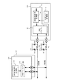
まず、従来のDDRタイプのメモリ装置の課題について説明する。図1は、メモリ装置およびメモリ制御装置を含むシステムのブロック図である。図1を参照に、CPU(中央演算処理装置)165およびメモリ制御装置100がバス160に接続されている。メモリ制御装置100には、2つのメモリ装置110および120が接続されている。メモリ制御装置100は、2つのメモリ装置110および120を制御し、CPU165から出力されたデータをメモリ装置110または120に記憶させる。また、メモリ装置110または120からデータを読み出し、CPU165に出力する。ここで、例えば、メモリ装置110は512MbyteのDDR−SDRAM(ダブル・データ・レート・シンクロナス・ダイナミック・ランダム・アクセス・メモリ)であり、メモリ装置120は、1GbyteのDDR−NORフラッシュメモリ(ダブル・データ・レート・シンクロナス・ノンボラタイル・アクセス・メモリ)である。
First, a problem of a conventional DDR type memory device will be described. FIG. 1 is a block diagram of a system including a memory device and a memory control device. Referring to FIG. 1, a CPU (Central Processing Unit) 165 and a
図2は、メモリ装置110とメモリ制御装置100との信号の入出力を示すタイミングチャートである。CK、/CKは差動クロック信号、CMDはコマンド信号、DQS、/DQSは差動ストローブ信号、DQはデータ信号を示している。コマンド信号CMDのNOPはデータの入出力に関係するコマンドが出力されていないことを示している。クロック信号上の数字はクロック周期を示している。初期状態では、メモリ装置110はデータの入出力を行っておらず、差動ストローブ信号も出力されていない。差動ストローブ信号は、データを出力する側の装置が出力する。すなわち、メモリ装置110または120からデータを読み出す際はメモリ装置110または120が差動ストローブ信号を出力し、メモリ装置110または120にデータを記憶する際はメモリ制御装置100が差動ストローブ信号を出力する。
FIG. 2 is a timing chart showing signal input / output between the
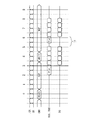
クロック周期0において、メモリ制御装置100は、メモリ装置110のメモリセルからデータを読み出すためのコマンドREAD1を出力する。2周期目にメモリ装置110は、プリアンブル期間Pre1を設けるため、差動ストローブ信号の一方をハイ、他方をローとする。3周期目から、メモリ装置110は、差動ストローブ信号をハイ/ローを交互に出力する。このように、プリアンブル期間Pre1を設けるのは、最初のデータを出力するための差動ストローブ信号のクロスポイントを形成するためである。メモリ装置110は、差動ストローブ信号のクロスポイントでデータを出力する。メモリ制御装置100は、差動ストローブ信号のクロスポイントでデータを受け取る。このように、プリアンブル制御は、データの入出力の直前に前記ストローブ信号のうち一方をハイ、他方をローに保持する制御である。
In
図3は、メモリ装置110とメモリ装置120がメモリ制御装置100にデータを出力する際の従来の課題を説明するためのタイミングチャートである。5周期目までの各信号はコマンド信号を除き図2と同じである。4周期目にメモリ制御装置100は、メモリ装置120のメモリセルからデータを読み出すためのコマンドREAD2を出力する。6周期目にメモリ装置120は、プリアンブル期間Pre2を設けるため、差動ストローブ信号の一方をハイ、他方をローとする。7周期目から、メモリ装置120は、差動ストローブ信号をハイ/ローを交互に出力しデータを出力する。メモリ制御装置100は、差動ストローブ信号のクロスポイントでデータを受け取る。
FIG. 3 is a timing chart for explaining a conventional problem when the
図3では、メモリ装置120がデータを出力する前にプリアンブル期間Pre2が必要なため、メモリ装置110からのデータ出力とメモリ装置120からのデータ出力との間に期間T1を設けることとなる。このため、高速なデータの入出力の妨げになる。
In FIG. 3, since the preamble period Pre2 is necessary before the
図4は、メモリ制御装置100がメモリ装置110からデータを読み出しおよび記憶する際の従来の課題を説明するためのタイミングチャートである。5周期目までの各信号はコマンド信号を除き図2と同じである。4周期目にメモリ制御装置100は、メモリ装置120のメモリセルにデータを記憶させるためのコマンドWRIT1を出力する。5周期目にメモリ制御装置100は、プリアンブル期間Pre2を設けるため、差動ストローブ信号の一方をハイ、他方をローとする。6周期目から、メモリ制御装置100は、差動ストローブ信号をハイ/ローを交互に出力しデータを出力する。メモリ制置120は、差動ストローブ信号のクロスポイントでデータを受け取る。
FIG. 4 is a timing chart for explaining a conventional problem when the
図4では、メモリ制御装置100がデータを出力する前にプリアンブル期間Pre2が必要なため、メモリ装置110からのデータ入力とデータ出力との間に期間T2を設けることとなる。このため、高速なデータの入出力の妨げになる。
In FIG. 4, since the preamble period Pre2 is required before the
このように、図1のシステムにおいては、プリアンブル期間も含め差動ストローブ信号はデータを出力する装置が出力する。このため、異なる装置がデータを続けて出力する場合、異なる装置同士は相手の装置がデータを出力するタイミングを認識できないため、データの入出力を行う期間の前に常にプリアンブル期間を挿入することになる。このような、メモリ装置110および120とメモリ制御装置100との間のデータの入出力に係る課題を解決するため、以下の実施例においては、メモリ制御装置100(能動装置)が、コマンドに基づいてデータの入出力を行う期間の間の期間のストローブ信号を制御することを特徴とする。メモリ制御装置100は、メモリ装置110(受動装置)および120(受動装置)にコマンドを出力する装置である。よって、メモリ制御装置100は、コマンドからメモリ装置110および120からデータが出力されるタイミングを認識することができる。これにより、プリアンブル期間を不要とすることができる。
As described above, in the system of FIG. 1, the differential strobe signal including the preamble period is output by a device that outputs data. For this reason, when different devices continuously output data, different devices cannot recognize the timing at which the other device outputs data. Therefore, the preamble period is always inserted before the data input / output period. Become. In order to solve such a problem related to data input / output between the
言い換えれば、図1のシステムにおいては、システム内のリード動作/ライト動作に関わらずメモリ制御装置100のみがプリアンブル制御を一括して行い、メモリ装置110および120はプリアンブル制御を行わない。一方、データが入出力する期間のデータ(ライトデータまたはリードデータ)に対応するストローブ信号の制御は、メモリ制御装置100、メモリ装置110および120が、それぞれの動作モード(ライトモード、リードモード)に対応して実施する。具体的には、ライトデータに対応するストローブ信号の制御は、メモリ制御装置100が実施し、リードデータに対応するストローブ信号の制御は、メモリ装置110および120が実施する。以下、図面を参照に実施例につき詳細に説明する。
In other words, in the system of FIG. 1, only the
図5は、メモリ装置110とメモリ制御装置100とを示すブロック図である。メモリ装置120の構成はメモリ装置110と同じであり説明を省略する。図5参照に、メモリ装置110は、メモリセルアレイ128、Xデコーダ126、Yデコーダ124、高電圧生成部123、制御部122、ストローブ信号入出力部112、データ入出力部114、コマンド入力部116およびアドレス入力部118を有している。メモリセルアレイ128内にはメモリセル130がマトリックス状に配置されている。複数のワードラインWLおよび複数のビットラインBLが交差するように配置されている。アドレス情報に基づき、Xデコーダ126が1つのワードラインWLを選択し、Yデコーダ124が1つのビットラインBLを選択することにより、1つのメモリセルを選択することができる。高電圧生成部123は、データをメモリセルに記憶または読み出すための電圧を生成する。
FIG. 5 is a block diagram showing the
制御部122は、入力されたコマンドCMD、アドレスADに基づき、Xデコーダ126およびYデコーダ124を制御する。また、高電圧生成部123に高電圧を生成させる。ストローブ信号入出力部112は、差動ストローブ信号DQSおよび/DQSを入出力する。データ入出力部114は、差動ストローブ信号DQSおよび/DQSのクロスポイントに合わせデータDQを入出力する。コマンド入力部116はコマンドCMDを入力し、コマンドCMDを制御部122に出力する。アドレス入力部118はアドレスADを入力し、アドレスADを制御部122に出力する。
The
メモリ制御装置100は、制御部90、ストローブ信号制御部10、データ入出力部94、コマンド出力部96およびアドレス出力部98を有している。制御部90は、CPUとデータの入出力を行う。また、制御部90は、ストローブ信号制御部10、データ入出力部94、コマンド出力部96およびアドレス出力部98を制御し、メモリ装置110にデータを入出力する。ストローブ信号制御部10は、差動ストローブ信号DQSおよび/DQSをデータストローブ線を介してメモリ装置110に入出力する。また、後述するように、データDQを入出力する期間の間の期間において、コマンドCMDに基づきまたは/およびコマンドCMDが出力してからの期間に応じ、ストローブ信号DQSおよび/DQSのうち一方をハイ、他方をローに保持する。データ入出力部94は、メモリ装置110に、メモリセル130に記憶または読み出すデータDQをデータ線を介して入出力する。コマンド出力部96は、メモリ装置110に、データDQを入出力するためのコマンドCMDを出力する。アドレス出力部98は、メモリ装置110に、データDQのアドレスADを出力する。
The
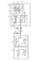
図6は、ストローブ信号DQSおよび/DQS信号の入出力を行う回路付近のブロック図である。ストローブ信号DQSおよび/DQS信号は、一対の差動線(DQS線および/DQS線:データストローブ線)を介しメモリ装置110とメモリ制御装置100との間で入出力される。DQS線は抵抗R11およびR12を介し例えば0.9Vの中間電位線VTTに接続される。抵抗R11とR12との間に抵抗R13が接続される。これにより、ストローブ信号が出力されないときは、DQS線は中間電位となる。/DQS線、抵抗R21、R22およびR23も同様である。
FIG. 6 is a block diagram of the vicinity of a circuit that inputs and outputs strobe signals DQS and / DQS. The strobe signals DQS and / DQS are input / output between the
メモリ制御装置100内では、コマンド制御部95がメモリ装置110または120に出力したコマンドの情報をストローブ信号制御部10内のDQS制御信号生成部50に出力する。DQS制御信号生成部50はコマンドに基づき、ストローブ信号のうち一方をハイ、他方をローに保持するためのDQS制御信号を生成し、ストローブ信号制御部10内のDQSバッファ12に出力する。DQS制御信号は、ストローブ信号のうち一方(DQS)をハイ、他方(/DQS)をローに保持する場合はハイ、保持しない場合はローである。DQSバッファ12は、DQS制御信号に基づきストローブ信号をDQS線および/DQS線に出力する。メモリ装置110および120は、それぞれDQSバッファ132およびDQS制御信号生成部134を有しており、ストローブ信号をDQS線および/DQS線に入出力する。
In the
図7は、DQS線に接続される回路の詳細を示すブロック図である。メモリ制御装置100内のDQSバッファ12は、OR回路14、インバータ16、PFET20、DQS入力バッファ40およびDQS出力バッファ42を有している。DQS制御信号生成部50から出力されるDQS制御信号とパワーダウン信号生成部60から出力されるパワーダウン信号がOR回路14に入力する。パワーダウン信号は、メモリ装置110または120をパワーダウンさせているときはロー、メモリ装置110または120をパワーオンさせているときはハイの信号である。
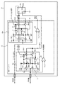
FIG. 7 is a block diagram showing details of a circuit connected to the DQS line. The
メモリ装置110または120がパワーオンしており、またはDQS制御信号がハイのとき、OR回路14の出力信号SBはハイである。よって、インバータ16の出力信号SAはローとなる。PFET20は高電圧線VDDとDQS線との間に接続されており、信号SAがローのとき高電圧線VDDとDQS線との間を接続し、ハイのとき遮断する。DQS線にはDQS入力バッファ40とDQS出力バッファ42が接続されている。DQS入力バッファ40は、DQS線の電位が参照電圧Vref(例えば0.9V)以上か否かでハイまたはローを内部回路に出力する。DQS出力バッファ42は、メモリ制御装置100がメモリ装置110または120にデータを出力する期間に、H/L信号に基づき、DQS線にハイおよびローをクロック信号に同期し周期的に出力する。
When the
メモリ装置110および120はそれぞれDQS出力バッファ140および150とDQS入力バッファ142および152とを有している。DQS出力バッファ140および150は、メモリ装置110または120がメモリ制御装置100にデータを出力する期間に、H/L信号に基づき、DQS線にハイおよびローをクロック信号に同期し周期的に出力する。DQS入力バッファ142および152は、DQS線の電位が参照電圧Vref(例えば0.9V)以上か否かでハイまたはローを内部回路に出力する。
図8は、/DQS線に接続される回路の詳細を示すブロック図である。メモリ制御装置100内のDQSバッファ12は、NFET22、DQS入力バッファ44およびDQS出力バッファ46を有している。NFET20は低電源線(例えばグランド)と/DQS線との間に接続されており、図7のOR回路の出力信号SBがハイのとき低電源線とDQS線との間を接続し、ローのとき遮断する。DQS入力バッファ44およびDQS出力バッファ46の動作は、図7のDQS入力バッファ40およびDQS出力バッファ42の動作と同じであり説明を省略する。
FIG. 8 is a block diagram showing details of a circuit connected to the / DQS line. The
メモリ装置110および120はそれぞれDQS出力バッファ144および154とDQS入力バッファ146および156とを有している。DQS出力バッファ144、154およびDQS入力バッファ146、156の動作は、図7のDQS出力バッファ140、150およびDQS入力バッファ142、152の動作と同じであり説明を省略する。
図9は実施例1の動作を示すタイミングチャート、図10は、各コマンドと信号SA、SBの関係を示した図である。ここで、各コマンドについて説明する。メモリ装置110および120をパワーダウンの状態からパワーオンの状態にスタンバイさせるコマンドがスタンバイコマンドである。パワーダウン状態とは、例えば、メモリ装置110または120の高電圧生成部123が高電圧を生成していない状態であり、パワーオン状態とは、メモリ装置110または120の高電圧生成部123が高電圧を生成している状態である。メモリ装置110または120へのデータの出力を指示するコマンドがライトコマンド、メモリ装置110または120からのデータの入力を指示するコマンドがリードコマンド、メモリ装置へのデータの入出力を強制的に終了するコマンドがバーストストップコマンドである。ここで、リードコマンドおよびライトコマンドはメモリセル130へのデータの記憶または読み出しのため、メモリ装置110または120内のYデコーダ124にメモリセルアレイ128のビット線BLを選択させるコマンドである。アクティブコマンドは、メモリセル130へのデータの記憶または読み出しのため、メモリ装置110または120内のXデコーダ126にワード線WLを選択させるコマンドである。
FIG. 9 is a timing chart showing the operation of the first embodiment, and FIG. 10 is a diagram showing the relationship between each command and the signals SA and SB. Here, each command will be described. A command for making the
メモリ制御装置100がリードコマンドまたはライトコマンドを出力した後、一定クロック周期後にデータの入出力が開始される。また、メモリ制御装置100がバーストストップコマンドを出力した後、一定クロック周期後にデータの入出力が終了する。ここで、一定クロック周期をレイテンシCLという。また、入出力するデータ長をDLとする。1クロック周期でストローブ信号は2つのクロスポイントを有するから、1クロック周期で2データ長のデータが入出力される。すなわち、リードコマンドを出力した後、レイテンシCL後にデータの入出力が開始され、CL+DL/2後にデータの入出力が終了する。実施例1においては、データ読み出しのレイテンシCLは3、データ記憶のレイテンシCLは2である。
After the
図9および図10を参照に、まず、パワーダウンの状態では、信号SAはハイ、信号SBはローであり、DQSおよび/DQS信号は中間電位状態(例えば0.9V)である。メモリ制御装置100がメモリ装置110または120にスタンバイコマンドを出力すると、信号SAはロー、信号SBはハイとなる。よって、DQS信号がハイ(例えば1.5V)、/DQS信号がロー(例えば0.3V)となる。その後、メモリ制御装置100がメモリ装置110および120にアクティブコマンドを出力する。メモリ制御装置100がメモリ装置110にリードコマンドを出力すると、2.5周期目(リード1+CL−0.5)後に信号SAがハイ、信号SBがローになる。DQS信号および/DQS信号は中間電位状態に戻ろうとするが、時定数がクロック周期に対し長いため、DQS信号がハイ、/DQS信号がローの状態で3周期目となる。
Referring to FIGS. 9 and 10, first, in a power-down state, signal SA is high, signal SB is low, and DQS and / DQS signals are in an intermediate potential state (for example, 0.9 V). When the
3周期目(リード1+CL)には、メモリ装置110がデータを出力するため、DQS信号および/DQS信号をクロックCKと同じ周期で交互にハイ/ローを繰り返しデータを出力する。4周期目にメモリ制御装置100がメモリ装置120にリードコマンドを出力する。5周期目(リード1+CL+DL/2)にメモリ装置110からのデータ出力が終了すると、信号SAはロー、信号SBはハイとなり、DQS信号がハイ/DQS信号がローとなる。6.5周期目(リード2+CL−0.5)後に信号SAがハイ、信号SBがローになる。
In the third period (read 1 + CL), since the
7周期目(リード2+CL)には、メモリ装置120がデータを出力するため、DQS信号および/DQS信号を交互にハイ/ローを繰り返しデータを出力する。8周期目にメモリ制御装置100がメモリ装置110にライトコマンドを出力する。9周期目(リード2+CL+DL/2)にメモリ装置110からのデータ出力が終了すると、信号SAはロー、信号SBはハイとなり、DQS信号がハイ、/DQS信号がローとなる。9.5周期目(ライト+CL−0.5)後に信号SAがハイ、信号SBがローになる。10周期目(ライト+CL)に、メモリ制御装置100がデータを出力するため、DQS信号および/DQS信号を交互にハイ/ローを繰り返しデータを出力する。12周期目(ライト+CL+DL/2)にメモリ制御装置100からのデータ出力が終了すると、信号SAはロー、信号SBはハイとなり、DQS信号がハイ、/DQS信号がローとなる。パワーダウンすると、信号SAはハイ、信号SBはローとなり、DQS信号、/DQS信号は中間電位状態となる。
In the seventh cycle (read 2 + CL), since the
図11は実施例1の別の例である。この例では、メモリ制御装置100がメモリ装置110にアクティブコマンドを出力すると信号SAはロー、信号SBはハイとなる。よって、DQS信号がハイ、/DQS信号がローとなる。その他の動作は図9と同じである。
FIG. 11 shows another example of the first embodiment. In this example, when the
実施例1によれば、ストローブ信号制御部10は、スタンバイコマンドに基づき、DQS信号をハイ、/DQS信号をローとする。また、リードコマンドが出力されてから5周期目にDQS信号をハイ、/DQS信号をローとする。つまり、リードコマンドが出力してからの期間に応じて、DQS信号をハイ、/DQS信号をローとする。このように、ストローブ信号制御部10は、データを入出力する期間の間の期間においてコマンドに基づきまたは/およびコマンドが出力してからの期間に応じて、DQS信号をハイ、/DQS信号をローに保持する。メモリ制御装置100は、データを入出力するためのコマンドを出力する装置であるため、各装置がデータを入出力するタイミングを認識できる。よって、メモリ制御装置100のストローブ信号制御部10がコマンドに基づきデータを入出力する期間の間の期間における差動ストローブ信号を制御することにより、図3および図4のようにプリアンブル期間Pre1およびPre2を設けなくともよい。よって、メモリ装置110からデータを読み出した後、直ぐにメモリ装置120からデータを読み出すことができる。また、メモリ装置110からデータを読み出した後、直ぐにメモリ装置110にデータを記憶することができる。つまり入出力帯域の低下を抑制することができる。
According to the first embodiment, the strobe
また、図9のように、ストローブ信号制御部10は、コマンド出力部96がスタンバイコマンドを出力した後、最初のデータを入出力する期間の前にDQS信号をハイ、/DQS信号をローに保持する。これにより、最初にデータを入出力する際の最初にクロスポイントを設けることができる。
Further, as shown in FIG. 9, the strobe
また、図10のように、ストローブ信号制御部10は、コマンド出力部96が出力したアクティブコマンドに基づき、DQS信号をハイ、/DQS信号をローに保持することもできる。なお、アクティブコマンドは、メモリ装置からのデータの入出力を指示するという観点では、広義のリードコマンドまたはライトコマンドである。
Further, as shown in FIG. 10, the strobe
さらに、図9のように、ストローブ信号制御部10は、データが入出力する期間の前にストローブ信号をオフすることができる。これにより、データが入出力する期間において、データの入出力のタイミングを通知するためにストローブ信号を用いることができる。
Further, as shown in FIG. 9, the strobe
ストローブ信号制御部10は、コマンド出力部96がリードコマンドまたはライトコマンドを出力した後、所定時間後にストローブ信号をオフすることができる。データの入出力は、実施例1のように、リードコマンドまたはライトコマンド出力時から一定期間後に開始される。そこで、一定期間の例えば半周期前にストローブ信号がオフするように所定期間を規定することができる。
The strobe
実施例2は、DQS制御信号生成部の制御の例である。図12は、DQS制御信号生成部50の制御を説明するためのメモリ制御装置100のブロック図である。図12を参照に、DQS制御信号生成部50は、処理ロジック部52、要件A検出回路54、要件B検出回路56および要件C検出回路58を有している。コマンド制御部95はコマンドCMD、レイテンシCL、データ長DL、クロックCK、/CKを各要件検出回路54〜58およびメモリ装置110または120に出力する。コマンド制御部95は、パワーダウンに関するコマンドをパワーダウン信号生成部60に出力する。
The second embodiment is an example of control by the DQS control signal generation unit. FIG. 12 is a block diagram of the
各要件検出回路54〜58は各要件を満足するかを判定し、処理ロジック部52に結果を出力する。処理ロジック部52は各要件の判定に基づき、DQS制御信号を生成し、OR回路14に出力する。その他の構成は実施例1と同じであり説明を省略する。
Each
図13はDQS制御信号生成部50の処理を示すフローチャートである。図13を参照に、パワーダウンの状態で開始される。処理ロジック部52は、DQS制御信号としてローを出力する(ステップS10)。すなわち、信号SAはハイ、信号SBはローである。処理ロジック部52は、スタンバイかを判定する(ステップS12)。Noの場合、ステップS12に戻る。Yesの場合、処理ロジック部52は、DQS制御信号としてハイを出力する(ステップS14)。すなわち、信号SAはロー、信号SBはハイとなり、DQS信号はハイ、/DQS信号はローとなる。
FIG. 13 is a flowchart showing processing of the DQS control
要件A検出回路54は、要件Aを満足するか判定する(ステップS16)。Noの場合、処理ロジック部52は、パワーダウンかを判定する(ステップS18)。Noの場合、ステップS16に戻る。Yesの場合、ステップS20に進む。ステップS16でYesの場合、処理ロジック部52はDQS制御信号としてローを出力する(ステップS24)。要件B検出回路56は、要件Bを満足するかを判定する(ステップS26)。Noの場合、ステップS26に戻る。Yesの場合、要件C検出回路58は、要件Cを満足するか判定する(ステップS28)。Yesの場合、ステップS26に戻る。Noの場合、ステップS14に戻る。ステップS18でYesの場合、処理ロジック部52は終了かを判定する。Yesの場合、終了する。Noの場合、ステップS12に戻る。
The requirement
このように、処理ロジック部52は、DQS制御信号としてハイが出力されている期間に、要件Aを満足すると、DQS制御信号としてローを出力する。さらに、DQS制御信号としてローが出力されている期間に、要件Bを満足し、かつ要件Cを満足しない場合、DQS制御信号としてハイを出力する。
As described above, the
図14は、要件A、要件Bおよび要件Cの例を示し、図15は、各要件を説明するための図9と同じタイミングチャートである。図14および図15を参照に、要件Aは、リードコマンドまたはライトコマンド実行からCL−0.5クロックの時点である。すなわち、データが入出力される0.5クロック前にDQS制御信号がローとなる。 FIG. 14 shows an example of requirement A, requirement B, and requirement C, and FIG. 15 is the same timing chart as FIG. 9 for explaining each requirement. Referring to FIG. 14 and FIG. 15, the requirement A is a point of CL-0.5 clock from the execution of the read command or the write command. That is, the DQS control signal goes low 0.5 clocks before data is input / output.
要件Bは、リードコマンドまたはライトコマンド実行からCL+DL/2クロックの時点である。すなわち、データの入出力が終了した時点で、DQS制御信号がローとなる。また、要件Bは、バーストストップコマンドが実行からCLクロックの時点である。すなわち、データ読み出し、またはデータ記憶が強制終了された時点で、DQS制御信号がローとなる。 The requirement B is a time point of CL + DL / 2 clock from the execution of the read command or the write command. That is, when the input / output of data is completed, the DQS control signal becomes low. Requirement B is the time when the burst stop command is CL clock from the execution. In other words, the DQS control signal becomes low when data reading or data storage is forcibly terminated.
要件Cは、リードコマンド、ライトコマンドまたはバーストストップコマンドが実行された後、所定期間内にリードコマンドまたはライトコマンドが入力された場合である。 Requirement C is a case where a read command or a write command is input within a predetermined period after a read command, a write command or a burst stop command is executed.
実施例2のように、ストローブ信号制御部10は、スタンバイコマンド、ライトコマンド、リードコマンド、バーストストップコマンドの少なくとも1つに基づき、DQS信号をハイ、/DQS信号をローに保持することができる。このように、ストローブ信号制御部10がコマンドに基づきストローブ信号を制御することにより、不要なプリアンブル期間を設ける必要がなく、データの入出力を高速に行うことができる。
As in the second embodiment, the strobe
図13のステップS26がYesであっても、ステップS28においてYesであればDQS制御信号はハイとはならない。図14を参照に、データの入出力終了後、直ぐに他のデータ入出力の入出力を開始する場合、DQS制御信号はローとならず、ハイのままである。すなわち、データの入出力が終了するとプリアンブル期間に入るが、直ぐに他のデータ入出力の入出力を開始する場合、プリアンブル期間を設けない。このように、ストローブ信号制御部10は、データの入出力の状況、データ線上のデータの混み具合に基づき、プリアンブル制御を行うか否かを制御することができる。このように、ストローブ信号制御部10は、コマンドの情報により、データ線上のデータの混み具合を把握できるため、図4で説明したような不要なプリアンブル期間を設けない制御を行うことができる。よって、入出力帯域の低下を抑制することができる。
Even if Step S26 in FIG. 13 is Yes, the DQS control signal does not become high if Yes in Step S28. Referring to FIG. 14, when the input / output of another data input / output is started immediately after the data input / output is completed, the DQS control signal does not go low but remains high. That is, when the input / output of data ends, the preamble period starts. However, when the input / output of other data input / output is started immediately, the preamble period is not provided. As described above, the strobe
また、データ入出力部94が連続してデータを入出力する場合、プリアンブル制御はなくてもよい。よって、この場合、ストローブ信号制御部10がプリアンブル制御を行わないことにより、入出力帯域の低下を抑制することができる。
Further, when the data input /
さらに、図14および図15の要件Cのように、コマンド出力部がリードコマンドまたはライトコマンドを出力した後、所定期間内にリードコマンドまたはライトコマンドを出力した場合、連続してデータの入出力が行われる。よって、この場合、ストローブ信号制御部10はプリアンブル制御を行わないことが好ましい。
Further, as shown in requirement C in FIGS. 14 and 15, when the command output unit outputs a read command or a write command within a predetermined period after outputting a read command or a write command, data is continuously input / output. Done. Therefore, in this case, it is preferable that the strobe
このように、ストローブ信号制御部10は、データ線を介したデータの入出力を把握できるため、プリアンブル制御を一括して行うことができる。これにより、従来のメモリ装置にも備えられていたプリアンブル制御を排除することができ、メモリ装置とメモリシステムの簡素化ができる。
Thus, since the strobe
実施例3は、DQSバッファの例である。図16は、DQSバッファ12内のDQS出力バッファ42および46の回路の詳細を示す図である。DQS出力バッファ42および46、フリップフロップ回路28以外の構成は実施例1と同じである。フリップフロップ回路28はクロック信号CKに同期しH/L信号を出力する。ここで、出力端子QZから出力されるH/L信号は出力端子QXから出力されるH/L信号の相補信号である。データ入出力信号は、データが入出力する期間にハイ、データが入出力しない期間にローとなる。リセット端子RSTにはリセット信号Resetが入力する。
The third embodiment is an example of a DQS buffer. FIG. 16 is a diagram showing details of the circuits of the DQS output buffers 42 and 46 in the
DQS出力バッファ42は、スイッチSW11〜SW14、インバータ33、PFET30およびNFET32を有している。データを入出力する期間においては、スイッチSW13およびSW14はオンし、スイッチSW11およびSW12はオフする。データを入出力しない期間においては、スイッチSW13およびSW14はオフし、スイッチSW11およびSW12はオンする。データを入出力する期間において、PFET30およびNFET32のゲートには、H/L信号が入力する。これにより、PFET30およびNFET32は、高電圧線VDDとグランドとを交互にDQS線に接続する。データを入出力しない期間において、PFET30のゲートはハイ、NFET32のゲートはローとなる。これにより、PFET30は、高電圧線VDDとDQS線との接続を遮断し、NFET32は、グランドとDQS線との接続を遮断する。
The
DQS出力バッファ46は、スイッチSW21〜SW24、インバータ39、PFET36およびNFET38を有しており、DQS出力バッファ42とは相補的に動作する。すなわち、DQS出力バッファ42がDQS線を高電圧線VDDに接続する期間、DQS出力バッファ46は/DQS線をグランドに接続する。DQS出力バッファ42がDQS線をグランドに接続する期間、DQS出力バッファ46は/DQS線を高電圧線VDDに接続する。
The
実施例3によれば、データを入出力する期間の間に期間において、PFET20(第1高電圧スイッチ)は、DQS信号対応するDQS線(差動線の一方)を高電圧線VDDに接続する。NFET22(第1低電圧スイッチ)は、/DQS信号に対応する/DQS線(差動線の他方)をグランド(低電圧線)に接続する。これにより、ストローブ信号制御部10は、データを入出力する期間の間の期間においてDQS信号をハイ、/DQS信号をローに保持することができる。
According to the third embodiment, the PFET 20 (first high voltage switch) connects the DQS line corresponding to the DQS signal (one of the differential lines) to the high voltage line VDD during a period between data input / output periods. . The NFET 22 (first low voltage switch) connects the / DQS line (the other of the differential lines) corresponding to the / DQS signal to the ground (low voltage line). Accordingly, the strobe
また、データを入出力する期間に、クロックに同期し、PFET30(第2高電圧スイッチ)は、DQS線を高電圧線VDDに接続し、NFET32(第2低電圧スイッチ)は、DQS線をグランドに接続する。また、クロックに同期し、PFET36(第3高電圧スイッチ)は、DQS線を高電圧線VDDに接続し、NFET38(第3低電圧スイッチ)は、DQS線をグランドに接続する。これにより、ストローブ信号制御部10は、データを入出力する期間においてストローブ信号を出力することができる。
Also, during the period of data input / output, in synchronization with the clock, the PFET 30 (second high voltage switch) connects the DQS line to the high voltage line VDD, and the NFET 32 (second low voltage switch) connects the DQS line to the ground. Connect to. In synchronization with the clock, the PFET 36 (third high voltage switch) connects the DQS line to the high voltage line VDD, and the NFET 38 (third low voltage switch) connects the DQS line to the ground. As a result, the strobe
さらに、PFET20は、データが入出力する期間の前にDQS線を高電圧線VDDから遮断し、NFET22は、データが入出力する期間の前に/DQS線をグランドから遮断する。これにより、データが入出力する期間にDQSバッファがストローブ信号を出力することができる。
Further, the
実施例4は、実施例3のPFET20とPFET30を共通とし、NFET22とNFET38を共通とした例である。図17は、DQSバッファ12内のDQS出力バッファ42aおよび46aの回路の詳細を示す図である。DQS出力バッファ42aにおいて、PFET20およびNFET22の機能をそれぞれPFET30およびNFET38が有している。
The fourth embodiment is an example in which the
DQS出力バッファ42a内のインバータ33の出力と信号SAとがAND回路31に入力し、AND回路31の出力がスイッチSW11に入力する。グランドとPFET30のゲートとの間にスイッチSW15が接続され、信号SAがインバータ35を介しスイッチSW15に入力する。
The output of the
DQS出力バッファ42b内のインバータ39の出力と信号SAとがAND回路37に入力し、AND回路37の出力がスイッチSW22に入力する。高電圧線VDDとNFET38のゲートとの間にスイッチSW26が接続され、信号SAがインバータ41を介しスイッチSW26に入力する。
The output of the
DQS線と高電圧線VDDを接続するFET、/DQS線とグランドとを接続するFETは大きくなる。そこで、実施例4のように、実施例3におけるPFET20とPFET30とを共通とし、NFET22とNFET38とを共通とすることもできる。これにより、回路面積を削減することができる。
The FET connecting the DQS line and the high voltage line VDD and the FET connecting the / DQS line and the ground become large. Therefore, as in the fourth embodiment, the
以上、本発明の好ましい実施例について詳述したが、本発明は係る特定の実施例に限定されるものではなく、特許請求の範囲に記載された本発明の要旨の範囲内において、種々の変形・変更が可能である。 The preferred embodiments of the present invention have been described in detail above, but the present invention is not limited to such specific embodiments, and various modifications can be made within the scope of the gist of the present invention described in the claims.・ Change is possible.
10 ストローブ信号制御部
94 データ入出力部
96 コマンド出力部
100 メモリ制御装置
110 メモリ装置
120 メモリ装置
130 メモリセル
DESCRIPTION OF
Claims (19)
前記メモリ装置に、前記データを入出力するためのコマンドを出力するコマンド出力部と、
前記データを入出力するタイミングを一対の差動信号のクロスポイントで通知するストローブ信号をデータストローブ線を介して前記メモリ装置に入出力し、前記データを入出力する期間の間の期間において、前記コマンドに基づきまたは/および前記コマンドが出力してからの期間に応じて、前記ストローブ信号のうち一方をハイ、他方をローに保持するストローブ信号制御部と、
を具備することを特徴とするメモリ制御装置。 An input / output unit for inputting / outputting data stored in or read from the memory cell via a data line to a memory device having a memory cell;
A command output unit for outputting a command for inputting / outputting the data to / from the memory device;
A strobe signal for notifying the timing of inputting / outputting the data at a cross point of a pair of differential signals is input / output to / from the memory device via a data strobe line. A strobe signal control unit that holds one of the strobe signals high and the other low according to a command or / and according to a period after the command is output;
A memory control device comprising:
前記差動線の前記一方を前記高電圧線に接続する第2高電圧スイッチと、
前記差動線の前記一方を前記低電圧線に接続する第2低電圧スイッチと、
前記差動線の前記他方を前記高電圧線に接続する第3高電圧スイッチと、
前記差動線の前記他方を前記低電圧線に接続する第3低電圧スイッチと、
を有することを特徴とする請求項6記載のメモリ制御装置。 The strobe signal control unit is configured to input / output the data,
A second high voltage switch connecting the one of the differential lines to the high voltage line;
A second low voltage switch connecting the one of the differential lines to the low voltage line;
A third high voltage switch connecting the other of the differential lines to the high voltage line;
A third low voltage switch connecting the other of the differential lines to the low voltage line;
7. The memory control device according to claim 6, further comprising:
前記第1低電圧スイッチは、前記データが入出力する期間の前に前記差動線の前記他方を前記低電圧線から遮断することを特徴とする請求項6または7記載のメモリ制御装置。 The first high voltage switch disconnects the one of the differential lines from the high voltage line before a period in which the data is input / output,
8. The memory control device according to claim 6, wherein the first low voltage switch cuts off the other of the differential lines from the low voltage line before a period in which the data is input and output.
前記メモリセルを有するメモリ装置に、前記メモリセルに記憶または読み出すデータをデータ線を介して入出力する入出力部と、
前記メモリ装置に、前記データを入出力するためのコマンドを出力するコマンド出力部と、
前記データを入出力するタイミングを一対の差動信号のクロスポイントで通知するストローブ信号をデータストローブ線を介して前記メモリ装置に入出力し、前記データを入出力する期間の間の期間において前記コマンドに基づきまたは/および前記コマンドが出力してからの期間に応じて、前記ストローブ信号のうち一方をハイ、他方をローに保持するストローブ信号制御部と、を有することを特徴とするメモリ制御装置と、
を具備することを特徴とするメモリシステム。 A memory device having memory cells;
An input / output unit for inputting / outputting data stored in or read from the memory cell via a data line to the memory device having the memory cell;
A command output unit for outputting a command for inputting / outputting the data to / from the memory device;
A strobe signal for notifying the timing of inputting / outputting the data at a cross point of a pair of differential signals is input / output to the memory device via a data strobe line, and the command is input during a period between the data input / output periods. And / or a strobe signal control unit that holds one of the strobe signals high and the other low according to a period after the command is output, and / or ,
A memory system comprising:
前記メモリ装置に、前記データを入出力するためのコマンドを出力するステップと、
前記データを入出力するタイミングを一対の差動信号のクロスポイントで通知するストローブ信号をデータストローブ線を介して前記メモリ装置に入出力するステップと、
前記データを入出力する期間の間の期間において前記コマンドに基づきまたは/および前記コマンドが出力してからの期間に応じて、前記ストローブ信号のうち一方をハイ、他方をローに保持するステップと、
を有することを特徴とするメモリ装置の制御方法。 Inputting / outputting data to / from the memory cell via a data line to a memory device having a memory cell;
Outputting a command for inputting and outputting the data to the memory device;
Inputting and outputting a strobe signal for notifying the timing of inputting and outputting the data at a cross point of a pair of differential signals to the memory device via a data strobe line;
Holding one of the strobe signals high and the other low, based on the command in a period between data input / output periods and / or according to a period after the command is output;
A method for controlling a memory device, comprising:
前記データを入出力するタイミングを一対の差動信号のクロスポイントで通知するストローブ信号をデータストローブ線を介して前記メモリ装置に入出力し、前記データ線の混み具合に基づき、前記データの入出力の直前に前記ストローブ信号のうち一方をハイ、他方をローに保持するプリアンブル制御を行うか否かを制御するストローブ信号制御部と、を具備するメモリ制御装置。 An input / output unit for inputting / outputting data stored in or read from the memory cell via a data line to a memory device having a memory cell;
A strobe signal for notifying the timing of inputting / outputting the data at a cross point of a pair of differential signals is input / output to the memory device via a data strobe line, and the input / output of the data is performed based on the degree of congestion of the data line. And a strobe signal control unit that controls whether or not to perform preamble control to hold one of the strobe signals high and the other low.
前記ストローブ信号制御部は、前記コマンド出力部が前記メモリ装置からのデータの入力を指示するリードコマンドまたは前記メモリ装置へのデータの出力を指示するライトコマンドを出力した後、所定期間内に前記リードコマンドまたは前記ライトコマンドを出力した場合、前記プリアンブル制御を行わないことを特徴とする請求項12記載のメモリ制御装置。 The memory device includes a command output unit that outputs a command for inputting and outputting the data,
The strobe signal control unit outputs the read command instructing the input of data from the memory device or the write command instructing the output of data to the memory device after the command output unit outputs the read command within a predetermined period. 13. The memory control device according to claim 12, wherein when the command or the write command is output, the preamble control is not performed.
前記メモリ装置に、前記メモリセルに記憶または読み出すデータをデータ線を介して入出力する入出力部と、
前記データを入出力するタイミングを一対の差動信号のクロスポイントで通知するストローブ信号をデータストローブ線を介して前記メモリ装置に入出力し、前記データ線の混み具合に基づき、前記データの入出力の直前に前記ストローブ信号のうち一方をハイ、他方をローに保持するプリアンブル制御を行うか否かを制御するストローブ信号制御部と、を具備するメモリシステム。 A memory device having memory cells;
An input / output unit for inputting / outputting data to be stored in or read from the memory cell via a data line to the memory device;
A strobe signal for notifying the timing of inputting / outputting the data at a cross point of a pair of differential signals is input / output to the memory device via a data strobe line, and the input / output of the data is performed based on the degree of congestion of the data line. A strobe signal control unit that controls whether or not to perform preamble control to hold one of the strobe signals high and the other low.
前記データを入出力するタイミングを一対の差動信号のクロスポイントで通知するストローブ信号をデータストローブ線を介して前記メモリ装置に入出力するステップと、
前記データ線の混み具合に基づき、前記データの入出力の直前に前記ストローブ信号のうち一方をハイ、他方をローに保持するプリアンブル制御を行うか否かを制御するステップと、
を有することを特徴とするメモリ装置の制御方法。 Inputting / outputting data to / from the memory cell via a data line to a memory device having a memory cell;
Inputting and outputting a strobe signal for notifying the timing of inputting and outputting the data at a cross point of a pair of differential signals to the memory device via a data strobe line;
Controlling whether or not to perform preamble control to hold one of the strobe signals high and the other low just before the data input / output based on the degree of congestion of the data line;
A method for controlling a memory device, comprising:
前記データを入出力するタイミングを一対の差動信号のクロスポイントで通知するストローブ信号をデータストローブ線を介して前記メモリ装置に入出力し、前記データの入出力の直前に前記ストローブ信号のうち一方をハイ、他方をローに保持するプリアンブル制御を一括して行うストローブ信号制御部と、を具備することを特徴とするメモリ制御装置。 An input / output unit for inputting / outputting data stored in or read from the memory cell via a data line to a memory device having a memory cell;
A strobe signal for notifying the timing of inputting / outputting the data at a cross point of a pair of differential signals is input / output to / from the memory device via a data strobe line, and one of the strobe signals is input immediately before the input / output of the data. And a strobe signal control unit for collectively performing preamble control for holding the other at low and the other at low.
前記メモリセルを有するメモリ装置に、前記メモリセルに記憶または読み出すデータをデータ線を介して入出力する入出力部と、
前記データを入出力するタイミングを一対の差動信号のクロスポイントで通知するストローブ信号をデータストローブ線を介して前記メモリ装置に入出力し、前記データの入出力の直前に前記ストローブ信号のうち一方をハイ、他方をローに保持するプリアンブル制御を一括して行うストローブ信号制御部と、を有することを特徴とするメモリ制御装置と、
を具備するメモリシステム。 A memory device having memory cells;
An input / output unit for inputting / outputting data stored in or read from the memory cell via a data line to the memory device having the memory cell;
A strobe signal for notifying the timing of inputting / outputting the data at a cross point of a pair of differential signals is input / output to / from the memory device via a data strobe line, and one of the strobe signals is input immediately before the input / output of the data. A memory control device having a strobe signal control unit that collectively performs preamble control that holds the other at low and the other at low,
A memory system comprising:
前記データを入出力するタイミングを一対の差動信号のクロスポイントで通知するストローブ信号をデータストローブ線を介して前記メモリ装置に入出力するステップと、
前記データの入出力の直前に前記ストローブ信号のうち一方をハイ、他方をローに保持するプリアンブル制御を一括して行うステップと、
を有することを特徴とするメモリ装置の制御方法。 Inputting / outputting data to / from the memory cell via a data line to a memory device having a memory cell;
Inputting and outputting a strobe signal for notifying the timing of inputting and outputting the data at a cross point of a pair of differential signals to the memory device via a data strobe line;
Performing a preamble control to hold one of the strobe signals high and the other low at the same time immediately before the input / output of the data;
A method for controlling a memory device, comprising:
Priority Applications (1)
| Application Number | Priority Date | Filing Date | Title |
|---|---|---|---|
| JP2008168467A JP5489427B2 (en) | 2008-06-27 | 2008-06-27 | Memory control device, memory system, and memory device control method. |
Applications Claiming Priority (1)
| Application Number | Priority Date | Filing Date | Title |
|---|---|---|---|
| JP2008168467A JP5489427B2 (en) | 2008-06-27 | 2008-06-27 | Memory control device, memory system, and memory device control method. |
Publications (2)
| Publication Number | Publication Date |
|---|---|
| JP2010009351A true JP2010009351A (en) | 2010-01-14 |
| JP5489427B2 JP5489427B2 (en) | 2014-05-14 |
Family
ID=41589761
Family Applications (1)
| Application Number | Title | Priority Date | Filing Date |
|---|---|---|---|
| JP2008168467A Active JP5489427B2 (en) | 2008-06-27 | 2008-06-27 | Memory control device, memory system, and memory device control method. |
Country Status (1)
| Country | Link |
|---|---|
| JP (1) | JP5489427B2 (en) |
Citations (4)
| Publication number | Priority date | Publication date | Assignee | Title |
|---|---|---|---|---|
| JP2000011646A (en) * | 1998-06-25 | 2000-01-14 | Fujitsu Ltd | Electronic device and semiconductor memory |
| JP2003346480A (en) * | 2002-05-25 | 2003-12-05 | Samsung Electronics Co Ltd | Semiconductor memory device having preamble function |
| JP2006134334A (en) * | 2004-11-04 | 2006-05-25 | Samsung Electronics Co Ltd | Memory unit which can raise efficiency of data strobe bus line, memory system provided with it, and control method of data strobe signal |
| JP2008103013A (en) * | 2006-10-18 | 2008-05-01 | Nec Electronics Corp | Memory read control circuit and its control method |
-
2008
- 2008-06-27 JP JP2008168467A patent/JP5489427B2/en active Active
Patent Citations (4)
| Publication number | Priority date | Publication date | Assignee | Title |
|---|---|---|---|---|
| JP2000011646A (en) * | 1998-06-25 | 2000-01-14 | Fujitsu Ltd | Electronic device and semiconductor memory |
| JP2003346480A (en) * | 2002-05-25 | 2003-12-05 | Samsung Electronics Co Ltd | Semiconductor memory device having preamble function |
| JP2006134334A (en) * | 2004-11-04 | 2006-05-25 | Samsung Electronics Co Ltd | Memory unit which can raise efficiency of data strobe bus line, memory system provided with it, and control method of data strobe signal |
| JP2008103013A (en) * | 2006-10-18 | 2008-05-01 | Nec Electronics Corp | Memory read control circuit and its control method |
Also Published As
| Publication number | Publication date |
|---|---|
| JP5489427B2 (en) | 2014-05-14 |
Similar Documents
| Publication | Publication Date | Title |
|---|---|---|
| US8547779B2 (en) | Memory circuits, systems, and method of interleavng accesses thereof | |
| KR100719377B1 (en) | Semiconductor memory device reading out data pattern | |
| JP2014197445A (en) | Assisting write operations to data storage cells | |
| US8254201B2 (en) | Semiconductor memory device having power-saving effect | |
| US9837137B2 (en) | Semiconductor device | |
| JP2011054219A (en) | Ferroelectric memory and memory system | |
| JP2006294209A (en) | Multi-port memory device | |
| US10872653B2 (en) | Memory modules, memory systems, and methods of operating memory modules | |
| JP2008108417A (en) | Low power dram and its driving method | |
| US9076512B2 (en) | Synchronous nonvolatile memory device and memory system supporting consecutive division addressing DRAM protocol | |
| US8934317B2 (en) | Semiconductor memory devices having internal clock signals and memory systems including such memory devices | |
| JP2000306379A (en) | Semiconductor memory | |
| JP4044538B2 (en) | Semiconductor device | |
| US10762935B2 (en) | Semiconductor devices | |
| US9047936B2 (en) | Memory device having control circuitry for write tracking using feedback-based controller | |
| US7961528B2 (en) | Buffer control circuit of memory device | |
| JP4740737B2 (en) | Multi-port memory device | |
| US8432757B2 (en) | Semiconductor system and method for operating the same | |
| US10847206B2 (en) | Semiconductor devices for executing a column operation | |
| CN107527649B (en) | Memory device with improved delay and method of operating the same | |
| JP5489427B2 (en) | Memory control device, memory system, and memory device control method. | |
| JP2008192264A (en) | Semiconductor memory device | |
| KR100444703B1 (en) | Memory device having high bus efficiency of network and the operation method thereof and memory system including the same | |
| JP2005267354A (en) | Semiconductor device | |
| KR101708873B1 (en) | Semiconductor memory device |
Legal Events
| Date | Code | Title | Description |
|---|---|---|---|
| RD04 | Notification of resignation of power of attorney |
Free format text: JAPANESE INTERMEDIATE CODE: A7424 Effective date: 20100402 |
|
| RD03 | Notification of appointment of power of attorney |
Free format text: JAPANESE INTERMEDIATE CODE: A7423 Effective date: 20100616 |
|
| A621 | Written request for application examination |
Free format text: JAPANESE INTERMEDIATE CODE: A621 Effective date: 20110624 |
|
| RD03 | Notification of appointment of power of attorney |
Free format text: JAPANESE INTERMEDIATE CODE: A7423 Effective date: 20120830 |
|
| A977 | Report on retrieval |
Free format text: JAPANESE INTERMEDIATE CODE: A971007 Effective date: 20130319 |
|
| A131 | Notification of reasons for refusal |
Free format text: JAPANESE INTERMEDIATE CODE: A131 Effective date: 20130404 |
|
| A601 | Written request for extension of time |
Free format text: JAPANESE INTERMEDIATE CODE: A601 Effective date: 20130702 |
|
| A602 | Written permission of extension of time |
Free format text: JAPANESE INTERMEDIATE CODE: A602 Effective date: 20130705 |
|
| A521 | Request for written amendment filed |
Free format text: JAPANESE INTERMEDIATE CODE: A523 Effective date: 20130729 |
|
| A02 | Decision of refusal |
Free format text: JAPANESE INTERMEDIATE CODE: A02 Effective date: 20130904 |
|
| A521 | Request for written amendment filed |
Free format text: JAPANESE INTERMEDIATE CODE: A523 Effective date: 20131225 |
|
| A911 | Transfer to examiner for re-examination before appeal (zenchi) |
Free format text: JAPANESE INTERMEDIATE CODE: A911 Effective date: 20140106 |
|
| TRDD | Decision of grant or rejection written | ||
| A01 | Written decision to grant a patent or to grant a registration (utility model) |
Free format text: JAPANESE INTERMEDIATE CODE: A01 Effective date: 20140127 |
|
| A61 | First payment of annual fees (during grant procedure) |
Free format text: JAPANESE INTERMEDIATE CODE: A61 Effective date: 20140225 |
|
| R150 | Certificate of patent or registration of utility model |
Ref document number: 5489427 Country of ref document: JP Free format text: JAPANESE INTERMEDIATE CODE: R150 |
|
| S111 | Request for change of ownership or part of ownership |
Free format text: JAPANESE INTERMEDIATE CODE: R313111 |
|
| R350 | Written notification of registration of transfer |
Free format text: JAPANESE INTERMEDIATE CODE: R350 |
|
| R250 | Receipt of annual fees |
Free format text: JAPANESE INTERMEDIATE CODE: R250 |
|
| R250 | Receipt of annual fees |
Free format text: JAPANESE INTERMEDIATE CODE: R250 |
|
| R250 | Receipt of annual fees |
Free format text: JAPANESE INTERMEDIATE CODE: R250 |
|
| R250 | Receipt of annual fees |
Free format text: JAPANESE INTERMEDIATE CODE: R250 |
|
| R250 | Receipt of annual fees |
Free format text: JAPANESE INTERMEDIATE CODE: R250 |
|
| R250 | Receipt of annual fees |
Free format text: JAPANESE INTERMEDIATE CODE: R250 |
|
| S111 | Request for change of ownership or part of ownership |
Free format text: JAPANESE INTERMEDIATE CODE: R313113 |
|
| R350 | Written notification of registration of transfer |
Free format text: JAPANESE INTERMEDIATE CODE: R350 |
|
| R250 | Receipt of annual fees |
Free format text: JAPANESE INTERMEDIATE CODE: R250 |