JP2010005794A - Thermal head - Google Patents
Thermal head Download PDFInfo
- Publication number
- JP2010005794A JP2010005794A JP2008164313A JP2008164313A JP2010005794A JP 2010005794 A JP2010005794 A JP 2010005794A JP 2008164313 A JP2008164313 A JP 2008164313A JP 2008164313 A JP2008164313 A JP 2008164313A JP 2010005794 A JP2010005794 A JP 2010005794A
- Authority
- JP
- Japan
- Prior art keywords
- electrode
- thermal head
- scanning direction
- sub
- heat generating
- Prior art date
- Legal status (The legal status is an assumption and is not a legal conclusion. Google has not performed a legal analysis and makes no representation as to the accuracy of the status listed.)
- Granted
Links
Images


Classifications
-
- B—PERFORMING OPERATIONS; TRANSPORTING
- B41—PRINTING; LINING MACHINES; TYPEWRITERS; STAMPS
- B41J—TYPEWRITERS; SELECTIVE PRINTING MECHANISMS, i.e. MECHANISMS PRINTING OTHERWISE THAN FROM A FORME; CORRECTION OF TYPOGRAPHICAL ERRORS
- B41J2/00—Typewriters or selective printing mechanisms characterised by the printing or marking process for which they are designed
- B41J2/315—Typewriters or selective printing mechanisms characterised by the printing or marking process for which they are designed characterised by selective application of heat to a heat sensitive printing or impression-transfer material
- B41J2/32—Typewriters or selective printing mechanisms characterised by the printing or marking process for which they are designed characterised by selective application of heat to a heat sensitive printing or impression-transfer material using thermal heads
- B41J2/335—Structure of thermal heads
- B41J2/33505—Constructional details
- B41J2/3351—Electrode layers
-
- B—PERFORMING OPERATIONS; TRANSPORTING
- B41—PRINTING; LINING MACHINES; TYPEWRITERS; STAMPS
- B41J—TYPEWRITERS; SELECTIVE PRINTING MECHANISMS, i.e. MECHANISMS PRINTING OTHERWISE THAN FROM A FORME; CORRECTION OF TYPOGRAPHICAL ERRORS
- B41J2/00—Typewriters or selective printing mechanisms characterised by the printing or marking process for which they are designed
- B41J2/315—Typewriters or selective printing mechanisms characterised by the printing or marking process for which they are designed characterised by selective application of heat to a heat sensitive printing or impression-transfer material
- B41J2/32—Typewriters or selective printing mechanisms characterised by the printing or marking process for which they are designed characterised by selective application of heat to a heat sensitive printing or impression-transfer material using thermal heads
- B41J2/335—Structure of thermal heads
- B41J2/33505—Constructional details
- B41J2/33515—Heater layers
-
- B—PERFORMING OPERATIONS; TRANSPORTING
- B41—PRINTING; LINING MACHINES; TYPEWRITERS; STAMPS
- B41J—TYPEWRITERS; SELECTIVE PRINTING MECHANISMS, i.e. MECHANISMS PRINTING OTHERWISE THAN FROM A FORME; CORRECTION OF TYPOGRAPHICAL ERRORS
- B41J2/00—Typewriters or selective printing mechanisms characterised by the printing or marking process for which they are designed
- B41J2/315—Typewriters or selective printing mechanisms characterised by the printing or marking process for which they are designed characterised by selective application of heat to a heat sensitive printing or impression-transfer material
- B41J2/32—Typewriters or selective printing mechanisms characterised by the printing or marking process for which they are designed characterised by selective application of heat to a heat sensitive printing or impression-transfer material using thermal heads
- B41J2/335—Structure of thermal heads
- B41J2/33545—Structure of thermal heads characterised by dimensions
-
- B—PERFORMING OPERATIONS; TRANSPORTING
- B41—PRINTING; LINING MACHINES; TYPEWRITERS; STAMPS
- B41J—TYPEWRITERS; SELECTIVE PRINTING MECHANISMS, i.e. MECHANISMS PRINTING OTHERWISE THAN FROM A FORME; CORRECTION OF TYPOGRAPHICAL ERRORS
- B41J2/00—Typewriters or selective printing mechanisms characterised by the printing or marking process for which they are designed
- B41J2/315—Typewriters or selective printing mechanisms characterised by the printing or marking process for which they are designed characterised by selective application of heat to a heat sensitive printing or impression-transfer material
- B41J2/32—Typewriters or selective printing mechanisms characterised by the printing or marking process for which they are designed characterised by selective application of heat to a heat sensitive printing or impression-transfer material using thermal heads
- B41J2/335—Structure of thermal heads
- B41J2/33555—Structure of thermal heads characterised by type
- B41J2/3357—Surface type resistors
Landscapes
- Electronic Switches (AREA)
Abstract
Description
本発明は小型・薄型のサーマルプリンタに最適な構成を備えたサーマルヘッドに関する。 The present invention relates to a thermal head having an optimum configuration for a small and thin thermal printer.
サーマルプリンタの印刷部に搭載されるサーマルヘッドは、基板と、前記基板上において主走査方向(長手方向)に配設された複数のドライバICと、発熱素子と、前記発熱素子を被覆する保護層とを備えている。 A thermal head mounted on a printing unit of a thermal printer includes a substrate, a plurality of driver ICs arranged in a main scanning direction (longitudinal direction) on the substrate, a heating element, and a protective layer covering the heating element. And.
前記発熱素子は、前記基板上の主走査方向に延在させて形成されたグレーズガラス等からなる蓄熱層、主走査方向寸法(幅寸法)および副走査方向寸法(長さ寸法)が規定された一対の実効発熱部と該一対の実効発熱部の長さ方向一端側を連接させた連接部とが前記蓄熱層上に複数配列形成され、発熱部を構成する発熱抵抗体層、前記発熱抵抗体層の表面を被覆して、発熱素子の発熱部の平面的な大きさを規定する絶縁層、および、前記絶縁層上にオーバーレイして前記発熱抵抗体層に通電可能な配線パターンの電極層(電極)を有している。 The heat generating element has a heat storage layer made of glaze glass or the like formed extending on the substrate in the main scanning direction, a main scanning direction dimension (width dimension), and a sub-scanning direction dimension (length dimension). A plurality of a pair of effective heat generating portions and a plurality of connecting portions in which one end in the length direction of the pair of effective heat generating portions are connected to each other are formed on the heat storage layer, and the heat generating resistor layer constituting the heat generating portion, the heat generating resistor An insulating layer that covers the surface of the layer to define a planar size of the heat generating portion of the heat generating element, and an electrode layer of a wiring pattern that can be overlaid on the insulating layer and energized to the heating resistor layer ( Electrode).
前記電極層は、前記一対の実効発熱部および前記連接部の副走査方向における一端側を連結させる折り返し電極、前記一対の実効発熱部のうち一方の実効発熱部の副走査方向における他端側に接続され、対応する各ドライバICと接続された個別電極、および、前記一対の実効発熱部のうち他方の実効発熱部の副走査方向における他端側に接続された共通電極により形成されてなる(以上、特許文献1参照)。 The electrode layer is a folded electrode that connects one end side in the sub-scanning direction of the pair of effective heat generating portions and the connecting portion, and is disposed on the other end side in the sub-scanning direction of one effective heat generating portion of the pair of effective heat generating portions. It is formed by a connected individual electrode connected to each corresponding driver IC, and a common electrode connected to the other end side in the sub-scanning direction of the other effective heat generating portion of the pair of effective heat generating portions ( As described above, refer to Patent Document 1).
ここで、近年、携帯機器に搭載され、電池により駆動されるプリンタの需要から、前述のような構成を有するプリンタのサーマルヘッドも小型化が求められており、その結果、サーマルヘッドの発熱素子に通電する電極の配線パターンの形成領域の狭小化が必須となっている。 Here, in recent years, due to the demand for printers mounted on portable devices and driven by batteries, the thermal heads of printers having the above-described configuration have been required to be miniaturized. It is indispensable to narrow the formation area of the wiring pattern of the electrode to be energized.
また、駆動電源を電池とするサーマルヘッドは、低電圧にて十分な電力を得るために発熱抵抗が小さくなければならない。しかし、前述のように各電極の配線パターンの形成領域が狭いと、1個のドライバICに128ドット分の発熱素子が接続されるような場合には、前記配線パターンのバーサイズ(幅寸法、長さ寸法)を調整して配線抵抗を小さくすることは困難であり、また、各発熱素子間に抵抗値のばらつきが生じていた。この抵抗値のばらつきは、印刷の濃度むらを発生させるため、良好な印刷結果を得ることができないという問題も生じる。 Also, a thermal head using a battery as a driving power source must have a small heating resistance in order to obtain sufficient power at a low voltage. However, if the wiring pattern formation area of each electrode is narrow as described above, when a heating element for 128 dots is connected to one driver IC, the bar size (width dimension, It is difficult to reduce the wiring resistance by adjusting the length dimension), and the resistance value varies among the heating elements. This variation in resistance value causes uneven printing density, which causes a problem that a good printing result cannot be obtained.
これらの問題の対策法として、各発熱素子を構成する発熱抵抗体層の形成後に、その発熱抵抗体層に適当な電圧パルスを印加してその抵抗値を低下させて調整する方法等も考えられている(特許文献2参照)。しかしながら、このような調整は個々のヘッドに対して行なわなければならず、非常に煩雑であった。また、サーマルヘッドの製造工程が増えるため、コストアップの要因となっていた。 As a countermeasure against these problems, a method may be considered in which, after forming the heating resistor layer constituting each heating element, an appropriate voltage pulse is applied to the heating resistor layer and the resistance value is lowered to adjust. (See Patent Document 2). However, such adjustment has to be performed for each head, which is very complicated. In addition, the manufacturing process of the thermal head is increased, resulting in a cost increase.
また、各発熱素子を構成する発熱抵抗体の大きさを変化させることも一案ではあるが、個々のドットサイズが相違することとなり、印刷結果に歪みが発生してしまう。さらに、各発熱素子を構成する発熱抵抗体に対する通電補正(逆補正)を行なうことも考えられるが、製品としてのサーマルヘッドのばらつきや印刷パターンや印刷率によって補正率が異なってくるため、一律な通電補正は困難である。 In addition, although it is one idea to change the size of the heating resistor constituting each heating element, the individual dot sizes are different, and the printed result is distorted. Furthermore, it is conceivable to perform energization correction (reverse correction) to the heating resistors constituting each heating element, but the correction rate varies depending on the variation of the thermal head as a product, the printing pattern, and the printing rate. Energization correction is difficult.
また、サーマルプリンタの印刷部は、サーマルヘッドの発熱素子に対する選択的な通電による発熱と同時に、記録媒体に対する適切な加圧が必然動作である。よって、写真のような記録媒体表面の光沢度、写像性(映り込みの鮮明さ)の良好な印刷結果を得るためには、印刷時に記録媒体と接触するサーマルヘッド表面は段差がなく、平滑であることが好ましい。 In addition, the printing unit of the thermal printer is inevitably subjected to appropriate pressurization to the recording medium simultaneously with heat generation by selective energization of the heating element of the thermal head. Therefore, in order to obtain a printing result with good glossiness and image clarity (the sharpness of reflection) on the surface of a recording medium such as a photograph, the surface of the thermal head that comes into contact with the recording medium during printing is smooth and smooth. Preferably there is.
ここで、サーマルヘッドの最上層として形成される保護層の表面には、特に、その下層に形成される抵抗体層や電極層の厚みに起因する段差が形成される。一般に、抵抗体層の段差は0.1〜0.2μmと薄く、アルミニウム(Al)等からなる電極層の段差は0.7〜1.0μmであるため、特に、この電極層の厚みに起因する段差が印刷結果の品質に大きく影響していた。そこで、一般的には、この段差を除去するべく、保護層表面を研磨して平滑化を図る作業工程が実施されている(特許文献3、特許文献4参照)。
Here, on the surface of the protective layer formed as the uppermost layer of the thermal head, in particular, a step due to the thickness of the resistor layer and electrode layer formed thereunder is formed. In general, the step of the resistor layer is as thin as 0.1 to 0.2 μm, and the step of the electrode layer made of aluminum (Al) or the like is 0.7 to 1.0 μm. The difference in level greatly affected the quality of the printed results. Therefore, generally, an operation process for polishing and smoothing the surface of the protective layer is performed in order to remove the step (see
しかしながら、保護膜表面の段差を研磨等で除去する形状加工は二次加工となるため、作業工数が増え、また、段差除去後の発熱素子の形状のばらつき等、製造上の負荷が大きかった。 However, since the shape processing for removing the step on the surface of the protective film by polishing or the like is a secondary processing, the number of work steps increases, and the manufacturing load such as variation in the shape of the heating element after the step removal is large.
また、サーマルヘッドを小型化し、発熱素子の取個数を上げるため、発熱抵抗体を凸状に形成された蓄熱層の頂部ではなく、傾斜する位置に配置する場合がある。さらには、製造工程上、ウェハーの状態でのサーマルヘッド表面を研磨する場合も多い。この様な場合、凸状の蓄熱層の傾斜の最も深い角度となる部分(凸頂部よりも離れた位置)に配置された折り返し電極を、その曲率を失うことなく研磨する事は非常に困難であった。よって、折り返し電極の寸法は短いほど研磨作業が容易となるが、短すぎる場合は印画に必要な発熱抵抗体の発熱分布が形成されない。このため、折返し電極部が蓄熱しすぎると、インクリボンを引き剥がす際にインクリボンに対し、ダメージ(熱ダメージ)を与え、インクリボン切れやインクリボンシワ等の悪影響が発生することになる。 Further, in order to reduce the size of the thermal head and increase the number of heating elements, the heating resistor may be disposed at an inclined position instead of the top of the heat storage layer formed in a convex shape. Furthermore, the surface of the thermal head in the wafer state is often polished during the manufacturing process. In such a case, it is very difficult to polish the folded electrode arranged at the deepest angle of the convex heat storage layer (position far from the convex top) without losing its curvature. there were. Therefore, the shorter the dimension of the folded electrode, the easier the polishing work is. However, if it is too short, the heat generation distribution of the heating resistor necessary for printing is not formed. For this reason, if the folded electrode portion stores too much heat, the ink ribbon is damaged (thermal damage) when the ink ribbon is peeled off, and adverse effects such as ink ribbon breakage and ink ribbon wrinkles occur.
本発明は、前述したような課題を解決するためになされたもので、製造工程やコストを増やさずに、複数の発熱抵抗体の抵抗値の調整に頼ることなく、通電時の発熱分布を均等にして良好な印刷結果を得ることができる高品質なサーマルヘッドであって、特に、印刷結果の良好な光沢性、写像性を実現することができ、更に省電力性も兼ね備えたサーマルヘッドを提供することを目的とする。 The present invention has been made to solve the above-described problems, and does not increase the manufacturing process and cost, and does not rely on the adjustment of the resistance values of a plurality of heating resistors, so that the heat generation distribution during energization is uniform. A high-quality thermal head that can achieve good printing results, and in particular, can achieve good gloss and image clarity of the printed results, and also provides power savings The purpose is to do.
前記課題を解決するため、本発明に係るサーマルヘッドは、基板と、前記基板上において主走査方向に配列された複数のドライバICと、前記基板上に形成された蓄熱層、一対の実効発熱部が発熱抵抗体として前記蓄熱層上に複数配列形成されてなる発熱抵抗体層、および、前記発熱抵抗体層に通電可能にパターン形成された電極層を有する発熱素子と、前記発熱素子の表面を被覆する保護層とを備え、前記電極層は、前記一対の実効発熱部の前記主走査方向に直交する副走査方向における一端側を連結させる折り返し電極、前記一対の実効発熱部のうち一方の実効発熱部の副走査方向における他端側と対応するそれぞれのドライバICとに接続された個別電極、および、前記一対の実効発熱部のうち他方の実効発熱部の副走査方向における他端側に接続された共通電極により形成されてなるサーマルヘッドにおいて、前記折り返し電極は、各発熱抵抗体の発熱分布を等しくするように面積が加減調整されて形成されていることを特徴とする。 In order to solve the above problems, a thermal head according to the present invention includes a substrate, a plurality of driver ICs arranged in the main scanning direction on the substrate, a heat storage layer formed on the substrate, and a pair of effective heat generating portions. A heating element having a heating resistor layer formed by arranging a plurality of heating resistors on the heat storage layer, an electrode layer patterned to allow current to flow through the heating resistor layer, and a surface of the heating element. A protective layer for covering, the electrode layer is a folded electrode that connects one end side in the sub-scanning direction orthogonal to the main scanning direction of the pair of effective heating portions, and one of the effective heating portions of the pair of effective heating portions. An individual electrode connected to each driver IC corresponding to the other end side of the heat generating portion in the sub-scanning direction, and the other of the pair of effective heat generating portions in the sub-scanning direction of the other effective heat generating portion In the thermal head composed formed by a common electrode connected to a side, the folded electrode is characterized in that the area to equalize the heat generation distribution of the heating resistors are formed by subtraction adjustment.
このような構成を備えたサーマルヘッドにおいては、発熱抵抗体を構成する一対の実効発熱部に連接された折り返し電極の面積を加減調整することで、発熱素子の発熱抵抗体の熱分布をコントロールすることで、良好な印刷結果を得ることができる。また、折り返し電極側への放熱ロスを改善することにより、省電力化も図ることができる。 In the thermal head having such a configuration, the heat distribution of the heating resistor of the heating element is controlled by adjusting the area of the folded electrode connected to the pair of effective heating portions constituting the heating resistor. As a result, good printing results can be obtained. Moreover, power saving can be achieved by improving the heat dissipation loss to the folded electrode side.
また、本発明に係るサーマルヘッドは、対応するそれぞれのドライバICに接続される個別電極の配線パターンは、各ドライバICに対する配列において端部側に配置された個別電極よりも中央側に配置された個別電極の方が引き回し寸法が短くなるように放射状にパターン形成されており、前記折り返し電極は、各ドライバICに対する配列において端部側に配置された折返し電極よりも中央側に配置された折返し電極の方が面積が大きくなるようにパターン形成されていることを特徴とする。 In the thermal head according to the present invention, the wiring pattern of the individual electrodes connected to the corresponding driver ICs is arranged on the center side of the individual electrodes arranged on the end side in the arrangement with respect to each driver IC. The individual electrodes are formed in a radial pattern so that the lead-out dimensions are shorter, and the folded electrodes are arranged on the center side with respect to the folded electrodes arranged on the end side in the arrangement for each driver IC. It is characterized in that the pattern is formed so as to have a larger area.
このような構成を備えたサーマルヘッドにおいては、サーマルヘッドの主走査方向に配列された各発熱素子の発熱抵抗体の熱分布を略均一にすることができる。 In the thermal head having such a configuration, the heat distribution of the heating resistors of the heating elements arranged in the main scanning direction of the thermal head can be made substantially uniform.
具体的には、前記各折り返し電極の副走査方向における長さ寸法を変化させることにより、面積を加減調整することができる。 Specifically, the area can be adjusted by changing the length dimension of each folded electrode in the sub-scanning direction.
さらに、前記各折り返し電極の副走査方向における長さ寸法は、20μm以上50μm以下とされていることを特徴とする。 Further, the length dimension of each folded electrode in the sub-scanning direction is 20 μm or more and 50 μm or less.
このように各折り返し電極の副走査方向における長さ寸法を調整されたサーマルヘッドにおいては、印刷結果に電極層の厚みに起因する段差の影響が出にくく、また、製造加工において保護層を研磨する場合に、研磨作業がし易い。 Thus, in the thermal head in which the length dimension of each folded electrode in the sub-scanning direction is adjusted, the printing result is hardly affected by the step due to the thickness of the electrode layer, and the protective layer is polished in the manufacturing process. In some cases, polishing work is easy.
また、前記各折り返し電極の副走査方向における長さ寸法は、前記発熱素子の発熱部の副走査方向長さ寸法の30%以下とされていることを特徴とする。 The length dimension of each folded electrode in the sub-scanning direction is 30% or less of the length dimension in the sub-scanning direction of the heat generating portion of the heating element.
このように各折り返し電極の副走査方向における長さ寸法を調整されたサーマルヘッドにおいては、例えば、インクリボン等に与える熱ダメージを悪化させることがない。 Thus, in the thermal head in which the length dimension of each folded electrode in the sub-scanning direction is adjusted, for example, thermal damage given to the ink ribbon or the like is not deteriorated.
またさらに、副走査方向における前記発熱素子の発熱抵抗体中央から±200μmの範囲において、前記保護層下に積層された層の厚さに起因して発生する前記保護層の表面の段差が0.2μm以下とされていることを特徴とする。 Still further, in the range of ± 200 μm from the center of the heating resistor of the heating element in the sub-scanning direction, the level difference on the surface of the protective layer caused by the thickness of the layer laminated under the protective layer is 0. It is characterized by being 2 μm or less.
このような構成を備えたサーマルヘッドにおいては、記録媒体表面の光沢度、写像性(映り込みの鮮明さ)の良好な印刷結果を得ることが可能となる。 In the thermal head having such a configuration, it is possible to obtain a printing result with good glossiness and image clarity (the sharpness of reflection) on the surface of the recording medium.
このように、本発明のサーマルヘッドは、製造工程やコストを増やさずに、通電時の発熱抵抗体の発熱分布を均等にして良好な印刷結果を得ることができ、特に、印刷結果の良好な光沢性、写像性を実現することができ、更に省電力性も兼ね備えるといった優れた効果を奏する。 As described above, the thermal head of the present invention can obtain a good printing result by making the heat distribution of the heating resistor uniform when energized without increasing the manufacturing process and cost, and particularly the printing result is good. Glossiness and image clarity can be realized, and there is also an excellent effect of having power saving.
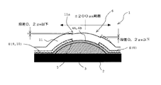
本実施形態のサーマルヘッド1は、図1に示すように、放熱性の基板2を備えている。前記基板2上には、記録方向と直交する主走査方向(記録紙の幅方向)に整列させて配設された複数のドライバIC(図示せず)が配設されている。また、前記基板2上には、ガラス等の断熱材料によってシリンドリカル状に形成された蓄熱層3と、発熱抵抗体4を構成する一対の実効発熱部4A,4Bが前記蓄熱層上に複数配列形成された発熱抵抗体層5と、各発熱抵抗体層5の表面を覆って発熱抵抗体4の平面的な大きさ、すなわち、記録方向と直交する主走査方向の寸法(幅寸法)および記録方向となる副走査方向の寸法(長さ寸法)を規定する絶縁層(図示せず)と、前記発熱抵抗体4上にオーバーレイして通電するAlからなる電極層Eとを有する発熱素子6が形成されている。また、発熱素子6を構成する発熱抵抗体層5、絶縁層及び電極層Eの表面を覆う耐磨耗性の保護層11が形成されている。なお、1つの実効発熱部4A,4Bは1つのドットを構成する。
As shown in FIG. 1, the
ここで、蓄熱層3は、放熱性基板2の表面全体に均一な膜厚で形成されたグレーズ層であり、主走査方向に延在させて形成されている。また、絶縁層は、例えばSiO2、SiON、SiAlON等の絶縁材料で形成されている。そして、発熱抵抗体層5は、Ta2N又はTa−SiO2等のサーメット材料を用いて蓄熱層3の上に部分的に形成されており、長さ寸法及び幅寸法の矩形状をなす一対の実効発熱部4A、4Bを有している。発熱抵抗体4は、発熱部にのみ、すなわち絶縁層の下層位置にのみ存在する。また、電極層Eは、一対の実効発熱部4A,4Bの副走査方向における一端側を連結させるように接続された折り返し電極8、一対の実効発熱部4A,4Bのうち一方の実効発熱部4Aの副走査方向における他端側に接続された個別電極9、および、一対の実効発熱部4A,4Bのうち他方の実効発熱部4Bの副走査方向における他端側に接続された共通電極10とを有している。
Here, the
そして、本実施形態において、前記折り返し電極8は、それぞれが接続された発熱抵抗体4の通電時の発熱分布を均等にするように、それぞれの面積が加減調整されて形成されており、本実施形態においては、図2に示すように、前記各折り返し電極8は、副走査方向における長さ寸法Bを変化させることにより面積が加減調整されている。このように、発熱抵抗体4を構成する一対の実効発熱部4A,4Bに連接された折り返し電極8の面積を加減調整して発熱素子6の発熱抵抗体4の熱分布をコントロールすることで、従来のように発熱抵抗体4の抵抗値の調整に拘らなくても、濃度むらのない、良好な印刷結果を得ることができる。
In the present embodiment, the folded
さらに詳しくは、本実施形態においては、各折り返し電極8は、その副走査方向における長さ寸法Bは20μm以上50μm以下とされており、さらには、前記発熱素子6の発熱部としての発熱抵抗体4の副走査方向長さ寸法Aの30%以下とされている。
More specifically, in the present embodiment, each folded
このような各折り返し電極8の副走査方向における長さ寸法Bのスペックを有するサーマルヘッド1は、印刷結果に電極層の厚みに起因する段差の影響が出にくく、また、製造加工において保護層を研磨する場合にも、研磨作業がし易いものとなる。さらに、前記発熱素子6の発熱抵抗体の副走査方向長さ寸法の30%以下とすることで、折り返し電極8の過分な蓄熱を抑え、インクリボンに与える熱ダメージを悪化させることを防止することができる。
The
また、個別電極9は、各発熱抵抗体4を個別に通電するための電極であり、発熱抵抗体4の長さ方向に延びる帯状電極で形成され、それぞれ対応する個別電極9への通電/非通電を切り替える複数のドライバICに接続されている。本実施形態においては、各ドライバICに接続される個別電極9の配線パターンは、各ドライバICに対する配列において端部側に配置された個別電極9よりも中央側に配置された個別電極9の方が引き回し寸法が短くなるように放射状(扇骨状)にパターン形成されている。また、前記折り返し電極8は、サーマルヘッド1の主走査方向に配列された各発熱素子6の発熱抵抗体4の熱分布を略均一にするべく、図3に示すように、各ドライバICに対する配列において端部側に配置された折り返し電極8よりも中央側に配置された折り返し電極8の方が面積が大きくなるようにパターン形成されている。本実施形態においては、通電時の発熱分布を均等にするべく、各発熱素子6の発熱抵抗体4の抵抗値と引き回し配線等に着目しつつ、折り返し電極8の面積が調整されている。
The
つまり、図3においては、各ドライバICは該ドライバICに対応する複数の発熱素子6の配列方向中央部に位置しており、これらの発熱素子6に接続された折り返し電極8は、前記配列方向中央から側方へ向かうにしたがって、その面積が小さくなるように、具体的には、副走査方向における長さ寸法を短くすることで、調整されている。
That is, in FIG. 3, each driver IC is located at the center in the arrangement direction of the plurality of
また、共通電極10は、複数の発熱抵抗体4に共通電位を与える電極である。共通電極10は、基板2の前記ドライバIC搭載側縁部で複数の発熱抵抗体4の配列方向にライン状に延び、同配列方向の両端から電源により給電されるライン電極部(図示せず)と、このライン電極部から前記発熱抵抗体4の長さ方向に延出して前記一対の実効発熱部4A,4Bのうちの他方の実効発熱部4Bに接続された複数のY字電極部とを有している。そして、前記個別電極9及び共通電極10のY字電極部は、発熱抵抗体4の一対の実効発熱部4A、4Bの幅寸法Wと略一致する幅寸法で形成され、それぞれの実効発熱部4A、4B側の端部が絶縁層6上にオーバーレイするようにして形成されている。
The
保護層11は、例えばSiAlONやTa2O5等の耐摩耗性材料からなり、ヘッド動作時に生じる摩擦から各発熱素子6の表面の絶縁層及び電極層E(折り返し電極8、個別電極9、共通電極10)を保護する。保護層11の厚さは一定のため、保護層11の表面には基板2の表面の凹凸形状、すなわち、保護層11の下に形成される層、特には、電極層Eの厚さに起因して発生する段差が転写されており、絶縁層の上方位置には印刷媒体との接触が良好となるように研磨加工された滑らかな段差部11aが設けられている(図1には、研磨により除去された部分を破線で示す)。本実施形態においては、図1に示すように、副走査方向における発熱素子6の発熱部となる発熱抵抗体4の中央から±200μmの範囲において、前記段差部11aの寸法が0.2μm以下となるように形成されている。このような段差寸法とすることで、印刷時に、サーマルヘッド1に通電した状態で印刷媒体にサーマルヘッド1を押圧しても、印刷媒体表面に前記凹凸形状を転写させることが無いので、記録媒体表面の光沢度、写像性(映り込みの鮮明さ)の良好な印刷結果を得ることが可能となる。
The
なお、図4は同じ長さ寸法(100μm)、幅寸法(30μm)に形成された発熱抵抗体4に接続させる折り返し電極8を前述のスペック(折返し長さ寸法30μm)で形成した本実施形態のサーマルヘッド1と、従来のサーマルヘッド1(折返し長さ寸法125μm)との発熱抵抗体4の表面温度を比較したグラフである。グラフのX軸における中央には、各発熱抵抗体4の長さ方向中央の温度(300℃を縦軸における100%とする)を示し、X軸において右側方向には前記折り返し電極8が形成された基板の端部側、左側方向には共通電極10、個別電極9が形成された基板の端部側の温度を示す。
FIG. 4 shows the present embodiment in which the folded
このグラフに示すように、本実施形態のサーマルヘッド1は、抵抗値および発熱中心温度を変化させることなく折り返し電極側への放熱ロスを改善することができる。つまり、本実施形態のサーマルヘッド1は従来のサーマルヘッド1に比べて発熱抵抗体4の両端側(特に、折り返し電極8側)において熱の逃げが少なく、蓄熱されていることが解る。よって、低電圧での駆動が実現でき、省電力化を図ることができる。そして、前述のように、個別電極8の配線パターンを放射状に形成した場合に配線抵抗が高くなる、配列方向両端側に形成された折り返し電極8の面積を小さくすることにより、印刷結果の濃度むらの問題を解消することができる。また、サーマルヘッド1を製造する場合においても、一旦、面積を調整された折り返し電極8のパターンマスクを作成してしまえば、その後は、特に変更を要せずに、そのパターンマスクを利用して配線パターンを印刷形成することができるので、コストもかからず、簡便に製作することが可能となる。
As shown in this graph, the
なお、本発明は、前述した実施の形態に限定されるものではなく、必要に応じて種々の変更が可能である。 In addition, this invention is not limited to embodiment mentioned above, A various change is possible as needed.
例えば、各発熱抵抗体の発熱分布を隣位する発熱抵抗体間で均一とすべく行なう、折り返し電極の面積の調整は、発熱抵抗体の抵抗値を基準として行なう場合に限らない。例えば、発熱温度や印刷状態に基づき、各折り返し電極の面積の調整を行うことも可能である。 For example, the adjustment of the area of the folded electrode, which is performed so that the heat generation distribution of each heat generation resistor is uniform between adjacent heat generation resistors, is not limited to the case where the resistance value of the heat generation resistor is used as a reference. For example, the area of each folded electrode can be adjusted based on the heat generation temperature and the printing state.
また、各ドライバICに対する発熱素子の配列は、前述のように、発熱素子の配列方向中央部に対応させてドライバICが配設される場合に限らない。よって、個別電極9の配線パターンの形状も、前述のような放射状に限らない。
Further, as described above, the arrangement of the heating elements for each driver IC is not limited to the case where the driver ICs are arranged corresponding to the central portion in the arrangement direction of the heating elements. Therefore, the shape of the wiring pattern of the
1 サーマルヘッド
2 基板
3 蓄熱層
4 発熱抵抗体
4A,4B 実効発熱部
5 発熱抵抗体層
6 発熱素子
E 電極層
8 折り返し電極
9 個別電極
10 共通電極
11 保護層
11a 段差部
DESCRIPTION OF
Claims (6)
前記基板上において主走査方向に配列された複数のドライバICと、
前記基板上に形成された蓄熱層、一対の実効発熱部が発熱抵抗体として前記蓄熱層上に複数配列形成されてなる発熱抵抗体層、および、前記発熱抵抗体層に通電可能にパターン形成された電極層を有する発熱素子と、
前記発熱素子の表面を被覆する保護層と
を備え、
前記電極層は、前記各一対の実効発熱部の前記主走査方向に直交する副走査方向における一端側を連結させるように接続された折り返し電極、前記一対の実効発熱部のうち一方の実効発熱部の副走査方向における他端側と対応するそれぞれのドライバICとに接続された個別電極、および、前記一対の実効発熱部のうち他方の実効発熱部の副走査方向における他端側に接続された共通電極により形成されてなるサーマルヘッドにおいて、
前記折り返し電極は、各発熱抵抗体の発熱分布を等しくするように面積が加減調整されて形成されていることを特徴とするサーマルヘッド。 A substrate,
A plurality of driver ICs arranged in the main scanning direction on the substrate;
A heat storage layer formed on the substrate, a pair of effective heat generating portions are formed as a heat generating resistor, and a plurality of heat generating resistor layers are formed on the heat storage layer, and the heat generating resistor layer is patterned to allow energization. A heating element having an electrode layer;
A protective layer covering the surface of the heating element,
The electrode layer is a folded electrode connected so as to connect one end side in the sub-scanning direction orthogonal to the main scanning direction of each pair of effective heat generating parts, and one effective heat generating part of the pair of effective heat generating parts. The individual electrodes connected to the respective driver ICs corresponding to the other end side in the sub-scanning direction, and the other effective heat generating part of the pair of effective heat generating parts connected to the other end side in the sub-scanning direction In the thermal head formed by the common electrode,
2. The thermal head according to claim 1, wherein the folded electrode is formed by adjusting an area so as to equalize a heat generation distribution of each heating resistor.
前記折り返し電極は、各ドライバICに対する配列において端部側に配置された折返し電極よりも中央側に配置された折返し電極の方が面積が大きくなるようにパターン形成されていることを特徴とする請求項1に記載のサーマルヘッド。 In the wiring pattern of the individual electrodes connected to the corresponding driver ICs, the individual electrodes arranged on the center side have a shorter drawing dimension than the individual electrodes arranged on the end side in the arrangement with respect to each driver IC. Are radially patterned,
The folded electrode is patterned so that the area of the folded electrode arranged on the center side is larger than that of the folded electrode arranged on the end side in the arrangement for each driver IC. Item 2. The thermal head according to Item 1.
Priority Applications (5)
| Application Number | Priority Date | Filing Date | Title |
|---|---|---|---|
| JP2008164313A JP5049894B2 (en) | 2008-06-24 | 2008-06-24 | Thermal head |
| AT09007690T ATE548195T1 (en) | 2008-06-24 | 2009-06-10 | THERMOHEAD |
| EP09007690A EP2138312B1 (en) | 2008-06-24 | 2009-06-10 | Thermal head |
| US12/483,795 US7889219B2 (en) | 2008-06-24 | 2009-06-12 | Thermal head |
| CN2009101475401A CN101612838B (en) | 2008-06-24 | 2009-06-18 | Thermal head |
Applications Claiming Priority (1)
| Application Number | Priority Date | Filing Date | Title |
|---|---|---|---|
| JP2008164313A JP5049894B2 (en) | 2008-06-24 | 2008-06-24 | Thermal head |
Publications (2)
| Publication Number | Publication Date |
|---|---|
| JP2010005794A true JP2010005794A (en) | 2010-01-14 |
| JP5049894B2 JP5049894B2 (en) | 2012-10-17 |
Family
ID=41152212
Family Applications (1)
| Application Number | Title | Priority Date | Filing Date |
|---|---|---|---|
| JP2008164313A Active JP5049894B2 (en) | 2008-06-24 | 2008-06-24 | Thermal head |
Country Status (5)
| Country | Link |
|---|---|
| US (1) | US7889219B2 (en) |
| EP (1) | EP2138312B1 (en) |
| JP (1) | JP5049894B2 (en) |
| CN (1) | CN101612838B (en) |
| AT (1) | ATE548195T1 (en) |
Cited By (2)
| Publication number | Priority date | Publication date | Assignee | Title |
|---|---|---|---|---|
| JP2011177976A (en) * | 2010-02-26 | 2011-09-15 | Kyocera Corp | Optical print head and image forming apparatus using the same |
| JP2011224902A (en) * | 2010-04-21 | 2011-11-10 | Alps Electric Co Ltd | Thermal head |
Families Citing this family (1)
| Publication number | Priority date | Publication date | Assignee | Title |
|---|---|---|---|---|
| JP2007331202A (en) * | 2006-06-14 | 2007-12-27 | Alps Electric Co Ltd | Platen and recorder |
Family Cites Families (12)
| Publication number | Priority date | Publication date | Assignee | Title |
|---|---|---|---|---|
| JPH03114845A (en) * | 1989-09-29 | 1991-05-16 | Ricoh Co Ltd | Substrate for forming heating element |
| JP3114845B2 (en) * | 1995-08-21 | 2000-12-04 | 株式会社日立製作所 | Fully automatic washing machine |
| JP2001038941A (en) * | 1999-08-02 | 2001-02-13 | Seiko Instruments Inc | Thermal head |
| JP2001162849A (en) * | 1999-12-07 | 2001-06-19 | Seiko Instruments Inc | Thermal head |
| JP2004255650A (en) | 2003-02-25 | 2004-09-16 | Kyocera Corp | Thermal head and thermal printer using it |
| JP2005224992A (en) | 2004-02-10 | 2005-08-25 | Sony Corp | Thermal head, its manufacturing method, and dye sublimation printer |
| JP2005231169A (en) * | 2004-02-19 | 2005-09-02 | Rohm Co Ltd | Thermal printing head |
| JP4712367B2 (en) * | 2004-12-10 | 2011-06-29 | ローム株式会社 | Thermal print head |
| JP4541229B2 (en) | 2005-05-18 | 2010-09-08 | アルプス電気株式会社 | Thermal head and manufacturing method thereof |
| JP2006335002A (en) | 2005-06-03 | 2006-12-14 | Fujifilm Holdings Corp | Thermal head |
| JP2008164313A (en) | 2006-12-27 | 2008-07-17 | Ace Giken:Kk | Moisture detection method |
| JP2008168485A (en) * | 2007-01-10 | 2008-07-24 | Toshiba Hokuto Electronics Corp | Thermal head |
-
2008
- 2008-06-24 JP JP2008164313A patent/JP5049894B2/en active Active
-
2009
- 2009-06-10 EP EP09007690A patent/EP2138312B1/en not_active Not-in-force
- 2009-06-10 AT AT09007690T patent/ATE548195T1/en active
- 2009-06-12 US US12/483,795 patent/US7889219B2/en not_active Expired - Fee Related
- 2009-06-18 CN CN2009101475401A patent/CN101612838B/en not_active Expired - Fee Related
Cited By (3)
| Publication number | Priority date | Publication date | Assignee | Title |
|---|---|---|---|---|
| JP2011177976A (en) * | 2010-02-26 | 2011-09-15 | Kyocera Corp | Optical print head and image forming apparatus using the same |
| JP2011224902A (en) * | 2010-04-21 | 2011-11-10 | Alps Electric Co Ltd | Thermal head |
| US8384751B2 (en) | 2010-04-21 | 2013-02-26 | Alps Electric Co., Ltd. | Thermal head |
Also Published As
| Publication number | Publication date |
|---|---|
| ATE548195T1 (en) | 2012-03-15 |
| US20090315966A1 (en) | 2009-12-24 |
| JP5049894B2 (en) | 2012-10-17 |
| CN101612838A (en) | 2009-12-30 |
| EP2138312A1 (en) | 2009-12-30 |
| US7889219B2 (en) | 2011-02-15 |
| CN101612838B (en) | 2011-05-04 |
| EP2138312B1 (en) | 2012-03-07 |
Similar Documents
| Publication | Publication Date | Title |
|---|---|---|
| US7170539B2 (en) | Thermal head, method for manufacturing the same, and method for adjusting dot aspect ratio of thermal head | |
| WO2005070683A1 (en) | Thermal print head | |
| US7965307B2 (en) | Thermal head and method of manufacturing thermal head | |
| WO2005080084A1 (en) | Thermal print head | |
| KR20070094540A (en) | Thermal head and printing device | |
| WO2006062151A1 (en) | Thermal print head | |
| JP5049894B2 (en) | Thermal head | |
| JP4541229B2 (en) | Thermal head and manufacturing method thereof | |
| JP3825047B2 (en) | Method for forming auxiliary electrode layer for common electrode pattern in thermal head | |
| JP5127384B2 (en) | Thermal head and thermal printer | |
| JPH08310024A (en) | Thin film type thermal print head and manufacture thereof | |
| JP2004155160A (en) | Thermal head and its manufacturing process | |
| JP2007245668A (en) | Thermal head and printer | |
| JP5425564B2 (en) | Thermal print head and thermal printer | |
| JP5329887B2 (en) | Thermal head | |
| JP2010179551A (en) | Thermal head and method for manufacturing the same | |
| JP4666972B2 (en) | Thermal head and thermal printer using the same | |
| JP2014189016A (en) | Thermal print head and thermal printer | |
| JP2005335289A (en) | Thermal printer | |
| JP2526911Y2 (en) | Thermal head | |
| JP2005335176A (en) | Thermal head | |
| JP5765951B2 (en) | Thermal head and method for polishing substrate edge of thermal head | |
| JP2011201190A (en) | Thermal print head and method for manufacturing the same | |
| JP2008162139A (en) | Thermal head and thermal printer with the same | |
| JP2011068049A (en) | Thermal head and thermal printer equipped with the same |
Legal Events
| Date | Code | Title | Description |
|---|---|---|---|
| A621 | Written request for application examination |
Free format text: JAPANESE INTERMEDIATE CODE: A621 Effective date: 20101119 |
|
| A977 | Report on retrieval |
Free format text: JAPANESE INTERMEDIATE CODE: A971007 Effective date: 20120606 |
|
| TRDD | Decision of grant or rejection written | ||
| A01 | Written decision to grant a patent or to grant a registration (utility model) |
Free format text: JAPANESE INTERMEDIATE CODE: A01 Effective date: 20120626 |
|
| A01 | Written decision to grant a patent or to grant a registration (utility model) |
Free format text: JAPANESE INTERMEDIATE CODE: A01 |
|
| A61 | First payment of annual fees (during grant procedure) |
Free format text: JAPANESE INTERMEDIATE CODE: A61 Effective date: 20120723 |
|
| FPAY | Renewal fee payment (event date is renewal date of database) |
Free format text: PAYMENT UNTIL: 20150727 Year of fee payment: 3 |
|
| R150 | Certificate of patent or registration of utility model |
Ref document number: 5049894 Country of ref document: JP Free format text: JAPANESE INTERMEDIATE CODE: R150 Free format text: JAPANESE INTERMEDIATE CODE: R150 |
|
| S533 | Written request for registration of change of name |
Free format text: JAPANESE INTERMEDIATE CODE: R313533 |
|
| R350 | Written notification of registration of transfer |
Free format text: JAPANESE INTERMEDIATE CODE: R350 |