JP2010003930A - データ伝送光電子装置 - Google Patents
データ伝送光電子装置 Download PDFInfo
- Publication number
- JP2010003930A JP2010003930A JP2008162441A JP2008162441A JP2010003930A JP 2010003930 A JP2010003930 A JP 2010003930A JP 2008162441 A JP2008162441 A JP 2008162441A JP 2008162441 A JP2008162441 A JP 2008162441A JP 2010003930 A JP2010003930 A JP 2010003930A
- Authority
- JP
- Japan
- Prior art keywords
- laser
- section
- frequency
- modulator
- active
- Prior art date
- Legal status (The legal status is an assumption and is not a legal conclusion. Google has not performed a legal analysis and makes no representation as to the accuracy of the status listed.)
- Granted
Links
Images


Landscapes
- Semiconductor Lasers (AREA)
Abstract
【解決手段】本発明は、追加の変調器306と、電子光効果により変調可能である屈折率と、前記変調器の屈折率の変調を提供するための手段213を有している、追加の変調器の屈折率は、出力パルスレーザ光の繰り返し周波数が変化するように変えられ、また、前記ウェイブガイド103は、更に、前記追加の変調器306を含む。
【選択図】図3
Description

ここで、gnは、差動ゲインを示す。poは、キャビティ内の平均光子密度である。τpは、キャビティ光子寿命である。
△nmodal=Γ×nmaterial’ [2式]
ここで、Γは、電子光効果を示す材料における光モードの光閉じ込め係数(optical confinement factor of the optical mode)である。
ν=Vgroup/L [3式]
縞の長さは、2つの表面、前方面116と後方面117の間の幾何学的距離である。
ここで、符号Pは、整数の主値が計算されることを示している。cは、光の速度である。
△n=(1/2)no 3(rF+sF2)
[5式]
ここで、Fは、電界強度である。noは、ゼロ電界における屈折率である。rおよびsは、線形電子光係数および二次電子光係数である。
△n=ηF2/△ω
[6式]
ここで、ηは、3×10⁻⁵meVcm2kV−2の状態にあるように概算された、いわゆる有能指数(figure of merit)である。行動([4式])は、最初、6nmと10nmの間の幅を有し、40meVまで離調する量子井戸に対して実験的に研究された。電子光効果は、より大きな離調(40meVから140meV)において、[4式]で与えられるよりもかなり早く減少する(M.P.Earnshow、D.W.E.Allshopらによる“Electrooptic Effects in GaAs-AlGaAs Narrow Coupled Quantum Wells”, IEEE Journal of Quantum Electronics, Vol.37(7), pp.897-904、同書, Vol. 37(8), p.1103(2001)、M.V.Kotlyarらによる“electrooptic tuning of InP-based microphotonic Fabry-Perot filters”, J. Lightwave Technology, vol.23, pp.2169-2174(2005)参照)。
[1] A.G.Weber、Wu Rongham、D.Bimbergらによる”High-frequency response of p-substrate buried crescent InGaAsP lasers”, J. Appl. Phys. 68, 2499(1990).
[2] D.Tauber、G.Wang、R.S.Geds、J.E.Bowers、L.A.Coldrenらによる“70 GHz relaxation oscillation in vertical cavity surface emitting laser”, IEEE Trans. Electron. Devices, 39, p.2652(1992).
[3] D.Tauber、G.Wang、R.S.Geds、J.E.Bowers、L.A.Coldresnらによる“70 GHz relaxation oscillation in a vertical cavity surface emitting laser”,Device Research Conference, 1992. Digest. 50th Annual, June 22-24, 1992 pp.0 81-0 82.
[4] S.M.Kim、Y.Wang、M.Keever、J.S.Harrisらによる“High-frequency Modulation Characteristics of 1.3μm InGaAs Quantum Dot Lasers”, IEEE Phot. Technol. Lett. 16, pp.377-379(2004).
[5] S.Weisser、E.C.Larkins、K.Czotscher、W.Benz、J.Daleiden、I.Esquivias、J.Fleissner、J.D.Ralston、B.Romero、R.E.Sah、A.Schonfelder、J.Rosenzweigらによる“Damping-limited modulation bandwidths up to 40 GHz in undoped short-cavity In0.35Ga0.65As-GaAs multiple-quantum-well lasers”, IEEE Photon. Technol. Lett. 8. pp.608-610(1996).
[6] T.Yoshoie、O.Painter、A.Scherer、D.Huffaker、D.Deppeらによる“Photonic crystal defect microcavities with indium arsenide quantum dots”, Laser and Electro−Optics Society 2000 Annual Meeting. LEOS 2000. 13th Annual Meeting. IEEE, Volume:2, 13-16 Nov. 2000 pp.415-416 vol.2.
[7] N.Ledentsov、D.Bimberg、V.M.Ustinov、M.V.Maximov、Zh.I.Alferov、V.P.Kalosha、J.A.Lottらによる“Interconnection between gain spectrum and cavity mode in a quantum dot vertical cavity laser”, Semicond. Sci. Technol. 14, pp.99-102(1999).
[8] R.Kingによる“2D VCSEL Arrays for Chip-Level Optical Interconnects”, Annual report 1999, Dept. of Optoelectronics, University of Ulm.
[9] A.N.Al-Omari、K.L.Learらによる“Polyimide-planarized vertical-cavity surface-emitting lasers with 17.0 GHz bandwidth”, IEEE Photon. Technol. Lett. Vol.16, pp.969-971(2004).
[10] P.Pepeljugoski、D.Kuchta、Y.Kwark、P.Pleunis、G.Kuytらによる“15.6 Gb/s transmission over 1 km of next generation multimode fiber”, IEEE Photon. Technol. Lett. 14, pp.717-719(2002).
[11] D.M.Kuchta、P.Pepeljugoski、Y.Kwarkらによる“VCSEL modulation at 20 Gb/s over 200m of multimode fiber using a 3.3 V SiGe laser driver IC”, Advanced Semiconductor Lasers and Applications/Ultraviolet and Blue Lasers and Their Applications/Ultralong Haul DWDM Transmission and Networking/WDM Components, 2001 Digest of the LEOS Summer Topical Meeting, 30 July-1 Aug. 2001 Pages:2.
[12] Won-Jin Choi、A.E.Bond、Jongwoo Kim、 Jiaming Zhang、R.Jambunathan、H.Foulk、S.O'Brien、J.Van Norman、D.Vandegrift、C.Wanamaker、J.Shakespeare、He Caoらによる“Low insertion loss and low dispersion penalty InGaAsP quantum-well high-speed electroabsorption modulator for 40 Gb/s very-short-reach, long-reach, and long-haul applications”, Journal of Lightwave Technology 20, pp.2052-2056(2002).
[13] N.Mineo、K.Yamada、K.Nakamura、S.Sakai、T.Ushikuboらによる“60 GHz band electroabsorption modulator module”, in Proc. OFC 1998, ThH4.
[14] F.Devaux、P.Bordes、A.Ougazzaden、M.Carre、F.Huffらによる“Experimental optimization of MQW electroabsorption modulators with up to 40 GHz bandwidths”, Electron. Lett., vol.30, pp.1347-1348(1994).
[15] A.H.Steinbach、I.Penn、N.Chokshi、D.Martin、K.Slomkowsk、W.Baun、N.Agrawal、R.Ben-Michael、M.A.Itzlerらによる“Equivalent circuit modelling of p-i-n photodiodes for 40 Gb/s receivers”, Lasers and Electro-Optics Society, 2002, LEOS 2002. The 15th Annual Meeting of the IEEE, Volume:2. 10-14 Nov. 2002, Pages:486-487 vol.2.
[16] E.Alekseev、D.Pavlidis、V.Ziegler、M.Berg、J.Dickmannらによる“77 GHz high-isolation coplanar transmit-receive switch using InGaAs/InP PIN diodes”, Gallium Arsenide Integrated Circuit(GaAs IC) Symposium, 1998. Technical Digest 1998., 20th Annual Meeting, 1-4 Nov. 1998. Pages:177-180.
[17] Y.Muramoto、T.Ishibashiらによる“InP/InGaAs pin photodiode structure maximizing bandwidth and efficiency”, Electronics Letters 39, 1749-1750(2003).
[18] A.Umbach、T.Engel、H.G.Bach、S.van Waasen、E.Droge、A.Strittmatter、W.Ebert、W.Passenberg、R.Steingruber、W.Schlaak、G.G.Mekonnen、G.Unterborsch、D.Bimbergらによる“Technology of InP-based 1.55 μm ultrafast OEMMICs: 40 Gbit/s broad-band and 38/60 GHz narrow-band photoreceivers”, IEEE J. Quantum Electron. 35, pp.1024-1031(1999).
[19] H.Fengらによる“Field-induced optical effect in a five-step asymmetric coupled quantum well with modified potential”, IEEE J. Quantum. Electron., vol.34, pp.1197-1208(1998).
[20] M.P.Earnshaw、D.W.E. Allsoppらによる“Electrooptic effect in GaAs-AlGaAs narrow coupled quantum wells”, IEEE J. Quantum. Electron., vol.37 pp.897-904(2001).
[21] M.V.Kotlyar、L.O'Faolain、A.B.Krysa、Th.F.Kraussらによる“Electrooptic tuning of InP-based microphotonic Fabry-Perot filters”, J. Lightwave Technology, vol.23, pp.2169-2174(2005).
[22] N.N.Ledentsov、V.A.Shchukin、D.Bimbergらによる“Merging Nanoepitaxy and Nanophotonics”, In:“Future Trends in Microelectronics: Up the Nano Creek”, ed. by S.Luryi、J.Xu、A.Zaslavsky、Wiley & Sons, New York(2006).
[23] I.Galbraith、B.RyvkinらのによるEmpirical determination of the electroabsorption coefficient in semiconductors”, J. Appl. Phys. 74, 4145(1984).
[24] D.S.Chelmaらによる“Room Temperature Excitonic Nonlinear Absorption and Refraction in GaAs/AlGaAs Multiple Quantum Well Structures”, IEEE Journal of Quantum Electronics, Vol.QE-20(3), pp.265-275(1984).
[25] J.E.Zucker、T.L.Hendrickson、C.A.Burrusらによる“Electro-optic phase modulation in GaAs/AlGaAs quantum well waveguides”, Applied Physics Ltters, Vol.52(12), pp.945-947(1988).
[26] J.S.Weinerらによる“Quadratic electro-optic effect due to the quantum-confined Stark effect in quantum wells”, Applied Physics Letters, Vol.50(13), pp.842-844(1987).
[27] J.E.Zuckerらによる“Quaternary quantum wells for electro-optic intensity and phase modulation at 1.3 and 1.55μm”, Applied Physics Letters, Vol,54(1), pp.10-12(1989).
A(t)=A0cos[φ(t)]
[7式]
ここで、時間依存あるいは変調周波数は、位相の時間微分である。
dφ/dt=Ω(t)=Ω0+△Ωcos(ωt)
[8式]
[7式]の時間依存光信号は、以下のように表される。
A(t)=A0cos[Ω0t+(△Ω/ω)sin(ωt)]
[9式]
[式9]は、周波数Ω0、(Ω0±ω)、(Ω0±2ω)等を有する異なる高調波信号の組みに展開可能である。
ここで、パラメータ[β=△Ω/ω]およびJn(β)は、第1種およびn次のベッセル関数である。
多くの実際の状態では、[β<<1]であり、[10式]中のより高次の高調波の振幅は、kと共に急速に減少する。
Claims (12)
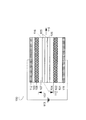
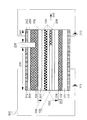
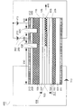
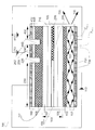
- フォワードバイアスが印加されると光ゲインを発生する活性要素を有する活性セクション(106)と、
吸収セクション(206)と、
前記活性セクションおよび前記吸収セクションを含むウェイブガイド(103)と、
光に対する帰還を提供するミラー(116、117)を備え、
前記ウェイブガイドは、前記ミラーの間に配置され、
該装置は、パルスレーザ光を放射するパルス体制において動作可能であり、
前記ウェイブガイド(103)は、更に、追加の変調器(306)を含むデータ伝送光電子装置(300)であって、
該装置は、周波数変調方法でデータ信号を伝送し、
前記追加の変調器(306)は、パルスレーザ光の繰り返し周波数が周波数変調され、また、周波数変調された光データ信号が発生されるように、屈折率を変調する。 - 請求項1に記載のデータ伝送装置であって、前記追加の変調器は、印加電界100keV/cmにおいて、少なくとも△n(%)=1%の屈折率の相対変化を提供する電子光効果を示す材料により構成されている。
- 請求項1または2に記載のデータ伝送装置であって、変調を提供する前記手段(213)は、少なくとも2つの異なる繰り返し周波数の間で繰り返し周波数を切り換えるスイッチを含んでいる。
- 請求項1〜3のいずれか1項に記載のデータ伝送装置であって、
前記活性セクションは、以下の(a)〜(j)からなるグループから選択される。
(a)端面発光ダイオードレーザ
(b)垂直キャビティ面発光レーザ
(c)端面発光幾何学で動作する傾斜キャビティレーザ
(d)表面発光幾何学で動作する傾斜キャビティレーザ
(e)基板の裏側からの反射を有する波長安定化漏洩波レーザ
(f)分布帰還型レーザ
(g)マイクロディスクレーザ
(h)フォトニック結晶レーザ
(i)少なくとも1つの外部ミラーを有するレーザ
(j)少なくとも1つのミラーが分布帰還型ミラーであるレーザ - 請求項1〜4のいずれか1項に記載のデータ伝送装置であって、前記吸収セクションは、前記ゲインセクションに統一され、また、単一のエピタキシャル処理で成長する。
- 請求項1〜5のいずれか1項に記載のデータ伝送装置であって、同じ媒体が、ゲイン媒体および電子光活性媒体として用いられている。
- 請求項1〜6のいずれか1項に記載のデータ伝送装置であって、電子光活性媒体として用いられる媒体は、ゲイン媒体として用いられる媒体と異なっている。
- 請求項1〜7のいずれか1項に記載のデータ伝送装置であって、前記電子光変調器および前記活性要素は、異なるキャビティ内に配置されている。
- 請求項1〜8のいずれか1項に記載のデータ伝送装置であって、
前記活性要素は、以下の(a)〜(e)からなるグループから選択される。
(a)量子井戸
(b)量子線のアレイ
(c)量子ドットのアレイ
(d)量子井戸、量子線あるいは量子ドットのスタック
(e)(a)〜(d)のいずれかの結合 - 請求項1〜9のいずれか1項に記載のデータ伝送装置であって、装置のアレイは、同じウェーハー上に組み立てられ、また、全ての装置は、多重チャンネル伝送に対して独立して動作する。
- パルス体制で動作可能なデータ伝送装置の活性セクション(106)の活性要素にフォワードバイアスを印加することによってパルスレーザ光を発生し、また、内部に光ゲインを発生する方法であり、
前記装置は、更に、吸収セクション(206)と、前記活性セクションおよび前記吸収セクションを含むウェイブガイド(103)と、光に対する帰還を提供するミラー(116、117)を含み、前記ウェイブガイドは、前記ミラーの間に配置されており、
データ信号は、周波数変調方法で伝送され、
装置のウェイブガイドによって組み入れられる追加の変調器(306)の屈折率は、パルスレーザ光の繰り返し周波数が周波数変調され、そして、周波数変調された光データ信号が発生されるように、変調される。 - 請求項11に記載の方法であって、パルスレーザ光は、少なくとも2つの異なる繰り返し周波数の間で繰り返し周波数を切り換えることによって周波数変調される。
Priority Applications (1)
| Application Number | Priority Date | Filing Date | Title |
|---|---|---|---|
| JP2008162441A JP5427371B2 (ja) | 2008-06-20 | 2008-06-20 | データ伝送光電子装置 |
Applications Claiming Priority (1)
| Application Number | Priority Date | Filing Date | Title |
|---|---|---|---|
| JP2008162441A JP5427371B2 (ja) | 2008-06-20 | 2008-06-20 | データ伝送光電子装置 |
Publications (2)
| Publication Number | Publication Date |
|---|---|
| JP2010003930A true JP2010003930A (ja) | 2010-01-07 |
| JP5427371B2 JP5427371B2 (ja) | 2014-02-26 |
Family
ID=41585390
Family Applications (1)
| Application Number | Title | Priority Date | Filing Date |
|---|---|---|---|
| JP2008162441A Expired - Fee Related JP5427371B2 (ja) | 2008-06-20 | 2008-06-20 | データ伝送光電子装置 |
Country Status (1)
| Country | Link |
|---|---|
| JP (1) | JP5427371B2 (ja) |
Cited By (4)
| Publication number | Priority date | Publication date | Assignee | Title |
|---|---|---|---|---|
| DE102015112981A1 (de) | 2014-08-08 | 2016-02-11 | Tokyo Institute Of Technology | Monolithisch integrierter oberflächenemittierender Laser mit Modulator |
| US9350139B2 (en) | 2013-08-07 | 2016-05-24 | Tokyo Institute Of Technology | Vertical-cavity surface-emitting laser diode and optical transmission apparatus |
| KR20200143410A (ko) * | 2019-06-14 | 2020-12-23 | 시아먼 유니버시티 | 전기적으로 주입되는 마이크로 디스크 공진 캐비티 발광 디바이스 및 그 제조 방법 |
| CN116799618A (zh) * | 2023-08-24 | 2023-09-22 | 武汉鑫威源电子科技有限公司 | 一种电调节垂直面发射氮化镓激光器 |
Families Citing this family (1)
| Publication number | Priority date | Publication date | Assignee | Title |
|---|---|---|---|---|
| CN112086856B (zh) * | 2020-10-13 | 2021-09-21 | 江苏华兴激光科技有限公司 | 一种半导体超短脉冲激光器及其制备方法 |
Citations (2)
| Publication number | Priority date | Publication date | Assignee | Title |
|---|---|---|---|---|
| JPH10135565A (ja) * | 1996-10-31 | 1998-05-22 | Oki Electric Ind Co Ltd | モード同期半導体レーザ及び繰返し周波数の可変方法 |
| JP2007165608A (ja) * | 2005-12-14 | 2007-06-28 | Oki Electric Ind Co Ltd | 受動モード同期半導体レーザ及び光クロック信号抽出装置 |
-
2008
- 2008-06-20 JP JP2008162441A patent/JP5427371B2/ja not_active Expired - Fee Related
Patent Citations (2)
| Publication number | Priority date | Publication date | Assignee | Title |
|---|---|---|---|---|
| JPH10135565A (ja) * | 1996-10-31 | 1998-05-22 | Oki Electric Ind Co Ltd | モード同期半導体レーザ及び繰返し周波数の可変方法 |
| JP2007165608A (ja) * | 2005-12-14 | 2007-06-28 | Oki Electric Ind Co Ltd | 受動モード同期半導体レーザ及び光クロック信号抽出装置 |
Cited By (8)
| Publication number | Priority date | Publication date | Assignee | Title |
|---|---|---|---|---|
| US9350139B2 (en) | 2013-08-07 | 2016-05-24 | Tokyo Institute Of Technology | Vertical-cavity surface-emitting laser diode and optical transmission apparatus |
| US9806498B2 (en) | 2013-08-07 | 2017-10-31 | Tokyo Institute Of Technology | Vertical-cavity surface-emitting laser diode and optical transmission apparatus |
| DE102015112981A1 (de) | 2014-08-08 | 2016-02-11 | Tokyo Institute Of Technology | Monolithisch integrierter oberflächenemittierender Laser mit Modulator |
| KR20160018396A (ko) | 2014-08-08 | 2016-02-17 | 고쿠리츠다이가쿠호진 토쿄고교 다이가꾸 | 광 변조 기능을 갖는 면발광 레이저 |
| KR20200143410A (ko) * | 2019-06-14 | 2020-12-23 | 시아먼 유니버시티 | 전기적으로 주입되는 마이크로 디스크 공진 캐비티 발광 디바이스 및 그 제조 방법 |
| KR102434130B1 (ko) * | 2019-06-14 | 2022-08-18 | 시아먼 유니버시티 | 전기적으로 주입되는 마이크로 디스크 공진 캐비티 발광 디바이스 및 그 제조 방법 |
| CN116799618A (zh) * | 2023-08-24 | 2023-09-22 | 武汉鑫威源电子科技有限公司 | 一种电调节垂直面发射氮化镓激光器 |
| CN116799618B (zh) * | 2023-08-24 | 2023-10-31 | 武汉鑫威源电子科技有限公司 | 一种电调节垂直面发射氮化镓激光器 |
Also Published As
| Publication number | Publication date |
|---|---|
| JP5427371B2 (ja) | 2014-02-26 |
Similar Documents
| Publication | Publication Date | Title |
|---|---|---|
| US7369583B2 (en) | Electrooptically wavelength-tunable resonant cavity optoelectronic device for high-speed data transfer | |
| US8290016B2 (en) | Optoelectric device for high-speed data transfer with electrooptically tunable stopband edge of a bragg-reflector | |
| US7580595B1 (en) | Data transmission optoelectric device | |
| US8218972B2 (en) | Wavelength division multiplexing system | |
| EP2525450B1 (en) | Reflectivity-modulated grating-mirror | |
| KR0147835B1 (ko) | 광장치 | |
| US7508858B2 (en) | Detuned duo-cavity laser-modulator device and method with detuning selected to minimize change in reflectivity | |
| US8970948B2 (en) | Method and system for operating semiconductor optical amplifiers | |
| EP2033282B1 (en) | Optoelectronic device for high-speed data transfer | |
| Nelson et al. | CW electrooptical properties of InGaAsP (λ= 1.3 µm) buried-heterostructure lasers | |
| JP5427371B2 (ja) | データ伝送光電子装置 | |
| Lee | Recent advances in long-wavelength semiconductor lasers for optical fiber communication | |
| Sato et al. | Actively mode-locked strained-InGaAsP multiquantum-well lasers integrated with electroabsorption modulators and distributed Bragg reflectors | |
| Fiedler et al. | Design of VCSEL's for feedback insensitive data transmission and external cavity active mode-locking | |
| Chang et al. | Design and performance of high-speed VCSELs | |
| US20060227823A1 (en) | Electroabsorption vertical cavity surface emitting laser modulator and/or detector | |
| Lim et al. | Modulation of a vertical-cavity surface-emitting laser using an intracavity quantum-well absorber | |
| EP1944842B1 (en) | Data transmission optoelectronic device | |
| JP4411938B2 (ja) | 変調器集積半導体レーザ、光変調システムおよび光変調方法 | |
| Kano et al. | High-speed intensity modulation of 1.5 mu m DBR lasers with wavelength tuning | |
| Ledentsov et al. | Novel approaches to semiconductor lasers | |
| Ou et al. | Mode Control and Dynamic Population Gratings in Quantum-Dot Lasers | |
| Choquette et al. | Vertical-cavity laser diode polarization switching and control | |
| Bimberg et al. | Quantum-dot based distributed feedback lasers and electro-absorption modulators for datacom applications | |
| Coldren | Lasers and modulators for OEICs |
Legal Events
| Date | Code | Title | Description |
|---|---|---|---|
| A621 | Written request for application examination |
Free format text: JAPANESE INTERMEDIATE CODE: A621 Effective date: 20110414 |
|
| A977 | Report on retrieval |
Free format text: JAPANESE INTERMEDIATE CODE: A971007 Effective date: 20120905 |
|
| A131 | Notification of reasons for refusal |
Free format text: JAPANESE INTERMEDIATE CODE: A131 Effective date: 20120913 |
|
| A601 | Written request for extension of time |
Free format text: JAPANESE INTERMEDIATE CODE: A601 Effective date: 20121212 |
|
| A602 | Written permission of extension of time |
Free format text: JAPANESE INTERMEDIATE CODE: A602 Effective date: 20121217 |
|
| A521 | Request for written amendment filed |
Free format text: JAPANESE INTERMEDIATE CODE: A523 Effective date: 20130115 |
|
| A131 | Notification of reasons for refusal |
Free format text: JAPANESE INTERMEDIATE CODE: A131 Effective date: 20130418 |
|
| A521 | Request for written amendment filed |
Free format text: JAPANESE INTERMEDIATE CODE: A523 Effective date: 20130628 |
|
| TRDD | Decision of grant or rejection written | ||
| A01 | Written decision to grant a patent or to grant a registration (utility model) |
Free format text: JAPANESE INTERMEDIATE CODE: A01 Effective date: 20131105 |
|
| A61 | First payment of annual fees (during grant procedure) |
Free format text: JAPANESE INTERMEDIATE CODE: A61 Effective date: 20131202 |
|
| R150 | Certificate of patent or registration of utility model |
Free format text: JAPANESE INTERMEDIATE CODE: R150 Ref document number: 5427371 Country of ref document: JP Free format text: JAPANESE INTERMEDIATE CODE: R150 |
|
| R250 | Receipt of annual fees |
Free format text: JAPANESE INTERMEDIATE CODE: R250 |
|
| R250 | Receipt of annual fees |
Free format text: JAPANESE INTERMEDIATE CODE: R250 |
|
| S111 | Request for change of ownership or part of ownership |
Free format text: JAPANESE INTERMEDIATE CODE: R313113 |
|
| R350 | Written notification of registration of transfer |
Free format text: JAPANESE INTERMEDIATE CODE: R350 |
|
| R250 | Receipt of annual fees |
Free format text: JAPANESE INTERMEDIATE CODE: R250 |
|
| R250 | Receipt of annual fees |
Free format text: JAPANESE INTERMEDIATE CODE: R250 |
|
| R250 | Receipt of annual fees |
Free format text: JAPANESE INTERMEDIATE CODE: R250 |
|
| R250 | Receipt of annual fees |
Free format text: JAPANESE INTERMEDIATE CODE: R250 |
|
| R250 | Receipt of annual fees |
Free format text: JAPANESE INTERMEDIATE CODE: R250 |
|
| R250 | Receipt of annual fees |
Free format text: JAPANESE INTERMEDIATE CODE: R250 |
|
| LAPS | Cancellation because of no payment of annual fees |