JP2010003853A - Base with bonding film, bonding method, and bonding structure - Google Patents
Base with bonding film, bonding method, and bonding structure Download PDFInfo
- Publication number
- JP2010003853A JP2010003853A JP2008161042A JP2008161042A JP2010003853A JP 2010003853 A JP2010003853 A JP 2010003853A JP 2008161042 A JP2008161042 A JP 2008161042A JP 2008161042 A JP2008161042 A JP 2008161042A JP 2010003853 A JP2010003853 A JP 2010003853A
- Authority
- JP
- Japan
- Prior art keywords
- bonding film
- bonding
- substrate
- base material
- film
- Prior art date
- Legal status (The legal status is an assumption and is not a legal conclusion. Google has not performed a legal analysis and makes no representation as to the accuracy of the status listed.)
- Granted
Links
- 238000000034 method Methods 0.000 title claims abstract description 210
- 239000000758 substrate Substances 0.000 claims abstract description 568
- 239000011344 liquid material Substances 0.000 claims abstract description 46
- 150000004696 coordination complex Chemical class 0.000 claims abstract description 43
- 229910052751 metal Inorganic materials 0.000 claims abstract description 40
- 239000002184 metal Substances 0.000 claims abstract description 39
- 238000001035 drying Methods 0.000 claims abstract description 15
- 239000000463 material Substances 0.000 claims description 273
- 238000005304 joining Methods 0.000 claims description 84
- 238000004381 surface treatment Methods 0.000 claims description 44
- 239000000126 substance Substances 0.000 claims description 42
- 239000012298 atmosphere Substances 0.000 claims description 37
- 239000010949 copper Substances 0.000 claims description 31
- 238000010438 heat treatment Methods 0.000 claims description 28
- 125000004429 atom Chemical group 0.000 claims description 26
- 125000002887 hydroxy group Chemical group [H]O* 0.000 claims description 25
- 230000008569 process Effects 0.000 claims description 24
- 239000011521 glass Substances 0.000 claims description 22
- 238000010304 firing Methods 0.000 claims description 19
- 230000001678 irradiating effect Effects 0.000 claims description 19
- 125000000217 alkyl group Chemical group 0.000 claims description 13
- 239000007787 solid Substances 0.000 claims description 12
- 229910052802 copper Inorganic materials 0.000 claims description 11
- RYGMFSIKBFXOCR-UHFFFAOYSA-N Copper Chemical compound [Cu] RYGMFSIKBFXOCR-UHFFFAOYSA-N 0.000 claims description 10
- XEEYBQQBJWHFJM-UHFFFAOYSA-N Iron Chemical compound [Fe] XEEYBQQBJWHFJM-UHFFFAOYSA-N 0.000 claims description 8
- 239000007769 metal material Substances 0.000 claims description 8
- 229910052782 aluminium Inorganic materials 0.000 claims description 7
- 229910052757 nitrogen Inorganic materials 0.000 claims description 7
- 125000004430 oxygen atom Chemical group O* 0.000 claims description 7
- 239000002210 silicon-based material Substances 0.000 claims description 7
- 125000004432 carbon atom Chemical group C* 0.000 claims description 6
- 229910052742 iron Inorganic materials 0.000 claims description 6
- 125000004435 hydrogen atom Chemical group [H]* 0.000 claims description 5
- 229910052707 ruthenium Inorganic materials 0.000 claims description 5
- 229910052725 zinc Inorganic materials 0.000 claims description 5
- 239000011701 zinc Substances 0.000 claims description 5
- 229910052799 carbon Inorganic materials 0.000 claims description 4
- 230000001747 exhibiting effect Effects 0.000 claims description 4
- 239000011261 inert gas Substances 0.000 claims description 4
- 239000012528 membrane Substances 0.000 claims description 4
- 238000009832 plasma treatment Methods 0.000 claims description 4
- KJTLSVCANCCWHF-UHFFFAOYSA-N Ruthenium Chemical compound [Ru] KJTLSVCANCCWHF-UHFFFAOYSA-N 0.000 claims description 3
- XAGFODPZIPBFFR-UHFFFAOYSA-N aluminium Chemical compound [Al] XAGFODPZIPBFFR-UHFFFAOYSA-N 0.000 claims description 3
- 125000000524 functional group Chemical group 0.000 claims description 3
- 125000005843 halogen group Chemical group 0.000 claims description 3
- 125000004433 nitrogen atom Chemical group N* 0.000 claims description 3
- 150000002978 peroxides Chemical class 0.000 claims description 3
- 125000004437 phosphorous atom Chemical group 0.000 claims description 3
- 229910052698 phosphorus Inorganic materials 0.000 claims description 3
- 229910052717 sulfur Inorganic materials 0.000 claims description 3
- 125000004434 sulfur atom Chemical group 0.000 claims description 3
- HCHKCACWOHOZIP-UHFFFAOYSA-N Zinc Chemical compound [Zn] HCHKCACWOHOZIP-UHFFFAOYSA-N 0.000 claims description 2
- 229910052736 halogen Inorganic materials 0.000 claims description 2
- 150000002367 halogens Chemical class 0.000 claims description 2
- 238000007142 ring opening reaction Methods 0.000 claims description 2
- 230000001070 adhesive effect Effects 0.000 abstract description 19
- 238000001354 calcination Methods 0.000 abstract 1
- 239000002585 base Substances 0.000 description 163
- 239000000976 ink Substances 0.000 description 72
- -1 polyethylene Polymers 0.000 description 55
- 239000000470 constituent Substances 0.000 description 34
- 239000010410 layer Substances 0.000 description 23
- 239000007789 gas Substances 0.000 description 19
- 239000000853 adhesive Substances 0.000 description 18
- 238000007639 printing Methods 0.000 description 18
- 239000002904 solvent Substances 0.000 description 17
- 208000028659 discharge Diseases 0.000 description 16
- IJGRMHOSHXDMSA-UHFFFAOYSA-N Atomic nitrogen Chemical compound N#N IJGRMHOSHXDMSA-UHFFFAOYSA-N 0.000 description 15
- 229910021421 monocrystalline silicon Inorganic materials 0.000 description 15
- 230000006870 function Effects 0.000 description 14
- 229920005989 resin Polymers 0.000 description 14
- 239000011347 resin Substances 0.000 description 14
- 238000011282 treatment Methods 0.000 description 13
- 238000011156 evaluation Methods 0.000 description 12
- 230000035882 stress Effects 0.000 description 11
- QVGXLLKOCUKJST-UHFFFAOYSA-N atomic oxygen Chemical compound [O] QVGXLLKOCUKJST-UHFFFAOYSA-N 0.000 description 10
- 230000000052 comparative effect Effects 0.000 description 10
- 239000001301 oxygen Substances 0.000 description 10
- 229910052760 oxygen Inorganic materials 0.000 description 10
- WEVYAHXRMPXWCK-UHFFFAOYSA-N Acetonitrile Chemical compound CC#N WEVYAHXRMPXWCK-UHFFFAOYSA-N 0.000 description 9
- 230000008859 change Effects 0.000 description 9
- JRBPAEWTRLWTQC-UHFFFAOYSA-N dodecylamine Chemical compound CCCCCCCCCCCCN JRBPAEWTRLWTQC-UHFFFAOYSA-N 0.000 description 9
- HFDWIMBEIXDNQS-UHFFFAOYSA-L copper;diformate Chemical class [Cu+2].[O-]C=O.[O-]C=O HFDWIMBEIXDNQS-UHFFFAOYSA-L 0.000 description 8
- XUIMIQQOPSSXEZ-UHFFFAOYSA-N Silicon Chemical compound [Si] XUIMIQQOPSSXEZ-UHFFFAOYSA-N 0.000 description 7
- 238000000576 coating method Methods 0.000 description 7
- 229910001873 dinitrogen Inorganic materials 0.000 description 7
- 239000000203 mixture Substances 0.000 description 7
- 239000005416 organic matter Substances 0.000 description 7
- 229910052710 silicon Inorganic materials 0.000 description 7
- 239000010703 silicon Substances 0.000 description 7
- ZWEHNKRNPOVVGH-UHFFFAOYSA-N 2-Butanone Chemical compound CCC(C)=O ZWEHNKRNPOVVGH-UHFFFAOYSA-N 0.000 description 6
- XKRFYHLGVUSROY-UHFFFAOYSA-N Argon Chemical compound [Ar] XKRFYHLGVUSROY-UHFFFAOYSA-N 0.000 description 6
- 125000001931 aliphatic group Chemical group 0.000 description 6
- 230000000694 effects Effects 0.000 description 6
- 239000007788 liquid Substances 0.000 description 6
- 230000007246 mechanism Effects 0.000 description 6
- 238000003825 pressing Methods 0.000 description 6
- 238000004891 communication Methods 0.000 description 5
- 238000009833 condensation Methods 0.000 description 5
- 230000005494 condensation Effects 0.000 description 5
- 230000018044 dehydration Effects 0.000 description 5
- 238000006297 dehydration reaction Methods 0.000 description 5
- 230000008030 elimination Effects 0.000 description 5
- 238000003379 elimination reaction Methods 0.000 description 5
- 239000004065 semiconductor Substances 0.000 description 5
- 239000000243 solution Substances 0.000 description 5
- 229910001220 stainless steel Inorganic materials 0.000 description 5
- 239000010935 stainless steel Substances 0.000 description 5
- 229910052723 transition metal Inorganic materials 0.000 description 5
- OKTJSMMVPCPJKN-UHFFFAOYSA-N Carbon Chemical compound [C] OKTJSMMVPCPJKN-UHFFFAOYSA-N 0.000 description 4
- IAZDPXIOMUYVGZ-UHFFFAOYSA-N Dimethylsulphoxide Chemical compound CS(C)=O IAZDPXIOMUYVGZ-UHFFFAOYSA-N 0.000 description 4
- ZMXDDKWLCZADIW-UHFFFAOYSA-N N,N-Dimethylformamide Chemical compound CN(C)C=O ZMXDDKWLCZADIW-UHFFFAOYSA-N 0.000 description 4
- 239000007983 Tris buffer Substances 0.000 description 4
- 230000003213 activating effect Effects 0.000 description 4
- 125000003342 alkenyl group Chemical group 0.000 description 4
- 125000000304 alkynyl group Chemical group 0.000 description 4
- 229910045601 alloy Inorganic materials 0.000 description 4
- 239000000956 alloy Substances 0.000 description 4
- 239000003575 carbonaceous material Substances 0.000 description 4
- 239000013078 crystal Substances 0.000 description 4
- 229910052739 hydrogen Inorganic materials 0.000 description 4
- 239000001257 hydrogen Substances 0.000 description 4
- 239000011133 lead Substances 0.000 description 4
- PXHVJJICTQNCMI-UHFFFAOYSA-N nickel Substances [Ni] PXHVJJICTQNCMI-UHFFFAOYSA-N 0.000 description 4
- 230000003287 optical effect Effects 0.000 description 4
- 229920000098 polyolefin Polymers 0.000 description 4
- 230000006798 recombination Effects 0.000 description 4
- 238000005215 recombination Methods 0.000 description 4
- 238000004528 spin coating Methods 0.000 description 4
- UHOVQNZJYSORNB-UHFFFAOYSA-N Benzene Chemical compound C1=CC=CC=C1 UHOVQNZJYSORNB-UHFFFAOYSA-N 0.000 description 3
- YMWUJEATGCHHMB-UHFFFAOYSA-N Dichloromethane Chemical compound ClCCl YMWUJEATGCHHMB-UHFFFAOYSA-N 0.000 description 3
- RTZKZFJDLAIYFH-UHFFFAOYSA-N Diethyl ether Chemical compound CCOCC RTZKZFJDLAIYFH-UHFFFAOYSA-N 0.000 description 3
- XEKOWRVHYACXOJ-UHFFFAOYSA-N Ethyl acetate Chemical compound CCOC(C)=O XEKOWRVHYACXOJ-UHFFFAOYSA-N 0.000 description 3
- OKKJLVBELUTLKV-UHFFFAOYSA-N Methanol Chemical compound OC OKKJLVBELUTLKV-UHFFFAOYSA-N 0.000 description 3
- 239000004721 Polyphenylene oxide Substances 0.000 description 3
- YXFVVABEGXRONW-UHFFFAOYSA-N Toluene Chemical compound CC1=CC=CC=C1 YXFVVABEGXRONW-UHFFFAOYSA-N 0.000 description 3
- 229910052786 argon Inorganic materials 0.000 description 3
- 230000008901 benefit Effects 0.000 description 3
- 239000011248 coating agent Substances 0.000 description 3
- 238000010894 electron beam technology Methods 0.000 description 3
- 229910002804 graphite Inorganic materials 0.000 description 3
- 239000010439 graphite Substances 0.000 description 3
- 230000010354 integration Effects 0.000 description 3
- 238000004519 manufacturing process Methods 0.000 description 3
- 230000015654 memory Effects 0.000 description 3
- 229910044991 metal oxide Inorganic materials 0.000 description 3
- 150000004706 metal oxides Chemical class 0.000 description 3
- 150000002739 metals Chemical class 0.000 description 3
- VLKZOEOYAKHREP-UHFFFAOYSA-N n-Hexane Chemical compound CCCCCC VLKZOEOYAKHREP-UHFFFAOYSA-N 0.000 description 3
- 229910052759 nickel Inorganic materials 0.000 description 3
- 150000004767 nitrides Chemical class 0.000 description 3
- 229910052763 palladium Inorganic materials 0.000 description 3
- 229920000728 polyester Polymers 0.000 description 3
- 229920006324 polyoxymethylene Polymers 0.000 description 3
- 238000000926 separation method Methods 0.000 description 3
- 229910052719 titanium Inorganic materials 0.000 description 3
- 239000010936 titanium Substances 0.000 description 3
- 229910052721 tungsten Inorganic materials 0.000 description 3
- DURPTKYDGMDSBL-UHFFFAOYSA-N 1-butoxybutane Chemical compound CCCCOCCCC DURPTKYDGMDSBL-UHFFFAOYSA-N 0.000 description 2
- KUFLEYZWYCAZCC-UHFFFAOYSA-N 2-methylhexa-1,3-diene Chemical compound CCC=CC(C)=C KUFLEYZWYCAZCC-UHFFFAOYSA-N 0.000 description 2
- UXFSPRAGHGMRSQ-UHFFFAOYSA-N 3-isobutyl-2-methoxypyrazine Chemical compound COC1=NC=CN=C1CC(C)C UXFSPRAGHGMRSQ-UHFFFAOYSA-N 0.000 description 2
- CSCPPACGZOOCGX-UHFFFAOYSA-N Acetone Chemical compound CC(C)=O CSCPPACGZOOCGX-UHFFFAOYSA-N 0.000 description 2
- QGZKDVFQNNGYKY-UHFFFAOYSA-N Ammonia Chemical compound N QGZKDVFQNNGYKY-UHFFFAOYSA-N 0.000 description 2
- CURLTUGMZLYLDI-UHFFFAOYSA-N Carbon dioxide Chemical compound O=C=O CURLTUGMZLYLDI-UHFFFAOYSA-N 0.000 description 2
- HEDRZPFGACZZDS-UHFFFAOYSA-N Chloroform Chemical compound ClC(Cl)Cl HEDRZPFGACZZDS-UHFFFAOYSA-N 0.000 description 2
- LFQSCWFLJHTTHZ-UHFFFAOYSA-N Ethanol Chemical compound CCO LFQSCWFLJHTTHZ-UHFFFAOYSA-N 0.000 description 2
- 229920000219 Ethylene vinyl alcohol Polymers 0.000 description 2
- YLQBMQCUIZJEEH-UHFFFAOYSA-N Furan Chemical compound C=1C=COC=1 YLQBMQCUIZJEEH-UHFFFAOYSA-N 0.000 description 2
- MHAJPDPJQMAIIY-UHFFFAOYSA-N Hydrogen peroxide Chemical compound OO MHAJPDPJQMAIIY-UHFFFAOYSA-N 0.000 description 2
- UQSXHKLRYXJYBZ-UHFFFAOYSA-N Iron oxide Chemical compound [Fe]=O UQSXHKLRYXJYBZ-UHFFFAOYSA-N 0.000 description 2
- CBENFWSGALASAD-UHFFFAOYSA-N Ozone Chemical compound [O-][O+]=O CBENFWSGALASAD-UHFFFAOYSA-N 0.000 description 2
- 239000004696 Poly ether ether ketone Substances 0.000 description 2
- 239000004952 Polyamide Substances 0.000 description 2
- 239000004372 Polyvinyl alcohol Substances 0.000 description 2
- KYQCOXFCLRTKLS-UHFFFAOYSA-N Pyrazine Chemical compound C1=CN=CC=N1 KYQCOXFCLRTKLS-UHFFFAOYSA-N 0.000 description 2
- JUJWROOIHBZHMG-UHFFFAOYSA-N Pyridine Chemical compound C1=CC=NC=C1 JUJWROOIHBZHMG-UHFFFAOYSA-N 0.000 description 2
- 229910052581 Si3N4 Inorganic materials 0.000 description 2
- VYPSYNLAJGMNEJ-UHFFFAOYSA-N Silicium dioxide Chemical compound O=[Si]=O VYPSYNLAJGMNEJ-UHFFFAOYSA-N 0.000 description 2
- PPBRXRYQALVLMV-UHFFFAOYSA-N Styrene Chemical compound C=CC1=CC=CC=C1 PPBRXRYQALVLMV-UHFFFAOYSA-N 0.000 description 2
- DTQVDTLACAAQTR-UHFFFAOYSA-N Trifluoroacetic acid Chemical compound OC(=O)C(F)(F)F DTQVDTLACAAQTR-UHFFFAOYSA-N 0.000 description 2
- MCMNRKCIXSYSNV-UHFFFAOYSA-N Zirconium dioxide Chemical compound O=[Zr]=O MCMNRKCIXSYSNV-UHFFFAOYSA-N 0.000 description 2
- 229920000122 acrylonitrile butadiene styrene Polymers 0.000 description 2
- 230000004913 activation Effects 0.000 description 2
- PNEYBMLMFCGWSK-UHFFFAOYSA-N aluminium oxide Inorganic materials [O-2].[O-2].[O-2].[Al+3].[Al+3] PNEYBMLMFCGWSK-UHFFFAOYSA-N 0.000 description 2
- 125000003277 amino group Chemical group 0.000 description 2
- 238000013459 approach Methods 0.000 description 2
- 238000007611 bar coating method Methods 0.000 description 2
- 238000005452 bending Methods 0.000 description 2
- 230000015572 biosynthetic process Effects 0.000 description 2
- HQABUPZFAYXKJW-UHFFFAOYSA-N butan-1-amine Chemical compound CCCCN HQABUPZFAYXKJW-UHFFFAOYSA-N 0.000 description 2
- 150000001721 carbon Chemical group 0.000 description 2
- 125000003178 carboxy group Chemical group [H]OC(*)=O 0.000 description 2
- 238000006243 chemical reaction Methods 0.000 description 2
- 229910052804 chromium Inorganic materials 0.000 description 2
- 150000001875 compounds Chemical class 0.000 description 2
- 230000006835 compression Effects 0.000 description 2
- 238000007906 compression Methods 0.000 description 2
- 229920001577 copolymer Polymers 0.000 description 2
- 230000006866 deterioration Effects 0.000 description 2
- 230000002542 deteriorative effect Effects 0.000 description 2
- 238000007599 discharging Methods 0.000 description 2
- 239000002270 dispersing agent Substances 0.000 description 2
- 239000002612 dispersion medium Substances 0.000 description 2
- 229920001971 elastomer Polymers 0.000 description 2
- 229920006332 epoxy adhesive Polymers 0.000 description 2
- 239000003822 epoxy resin Substances 0.000 description 2
- 238000005530 etching Methods 0.000 description 2
- GCSJLQSCSDMKTP-UHFFFAOYSA-N ethenyl(trimethyl)silane Chemical compound C[Si](C)(C)C=C GCSJLQSCSDMKTP-UHFFFAOYSA-N 0.000 description 2
- 239000005038 ethylene vinyl acetate Substances 0.000 description 2
- 229910052737 gold Inorganic materials 0.000 description 2
- 238000007756 gravure coating Methods 0.000 description 2
- LNEPOXFFQSENCJ-UHFFFAOYSA-N haloperidol Chemical compound C1CC(O)(C=2C=CC(Cl)=CC=2)CCN1CCCC(=O)C1=CC=C(F)C=C1 LNEPOXFFQSENCJ-UHFFFAOYSA-N 0.000 description 2
- 230000006872 improvement Effects 0.000 description 2
- 229910052741 iridium Inorganic materials 0.000 description 2
- ZXEKIIBDNHEJCQ-UHFFFAOYSA-N isobutanol Chemical compound CC(C)CO ZXEKIIBDNHEJCQ-UHFFFAOYSA-N 0.000 description 2
- 239000004973 liquid crystal related substance Substances 0.000 description 2
- 229910052748 manganese Inorganic materials 0.000 description 2
- 238000005259 measurement Methods 0.000 description 2
- BDAGIHXWWSANSR-UHFFFAOYSA-N methanoic acid Natural products OC=O BDAGIHXWWSANSR-UHFFFAOYSA-N 0.000 description 2
- 125000002496 methyl group Chemical group [H]C([H])([H])* 0.000 description 2
- 229910052750 molybdenum Inorganic materials 0.000 description 2
- 229910052758 niobium Inorganic materials 0.000 description 2
- 230000002093 peripheral effect Effects 0.000 description 2
- 238000007747 plating Methods 0.000 description 2
- 229910052697 platinum Inorganic materials 0.000 description 2
- 229920001200 poly(ethylene-vinyl acetate) Polymers 0.000 description 2
- 229920002647 polyamide Polymers 0.000 description 2
- 229920001707 polybutylene terephthalate Polymers 0.000 description 2
- 229920000647 polyepoxide Polymers 0.000 description 2
- 229920002530 polyetherether ketone Polymers 0.000 description 2
- 229920000139 polyethylene terephthalate Polymers 0.000 description 2
- 239000005020 polyethylene terephthalate Substances 0.000 description 2
- 229920000642 polymer Polymers 0.000 description 2
- 229920006380 polyphenylene oxide Polymers 0.000 description 2
- 229920002635 polyurethane Polymers 0.000 description 2
- 239000004814 polyurethane Substances 0.000 description 2
- 229920002451 polyvinyl alcohol Polymers 0.000 description 2
- 239000004800 polyvinyl chloride Substances 0.000 description 2
- 229920000915 polyvinyl chloride Polymers 0.000 description 2
- 230000009467 reduction Effects 0.000 description 2
- 239000005368 silicate glass Substances 0.000 description 2
- HQVNEWCFYHHQES-UHFFFAOYSA-N silicon nitride Chemical compound N12[Si]34N5[Si]62N3[Si]51N64 HQVNEWCFYHHQES-UHFFFAOYSA-N 0.000 description 2
- VZGDMQKNWNREIO-UHFFFAOYSA-N tetrachloromethane Chemical compound ClC(Cl)(Cl)Cl VZGDMQKNWNREIO-UHFFFAOYSA-N 0.000 description 2
- 230000008646 thermal stress Effects 0.000 description 2
- 125000003396 thiol group Chemical class [H]S* 0.000 description 2
- 238000009281 ultraviolet germicidal irradiation Methods 0.000 description 2
- 229910052720 vanadium Inorganic materials 0.000 description 2
- 229910052727 yttrium Inorganic materials 0.000 description 2
- 229910052726 zirconium Inorganic materials 0.000 description 2
- 125000004973 1-butenyl group Chemical group C(=CCC)* 0.000 description 1
- 125000006039 1-hexenyl group Chemical group 0.000 description 1
- RXUSTVIGZPRAQZ-UHFFFAOYSA-N 2,2,2-trifluoroacetic acid;yttrium Chemical compound [Y].OC(=O)C(F)(F)F.OC(=O)C(F)(F)F.OC(=O)C(F)(F)F RXUSTVIGZPRAQZ-UHFFFAOYSA-N 0.000 description 1
- XNWFRZJHXBZDAG-UHFFFAOYSA-N 2-METHOXYETHANOL Chemical compound COCCO XNWFRZJHXBZDAG-UHFFFAOYSA-N 0.000 description 1
- 125000000069 2-butynyl group Chemical group [H]C([H])([H])C#CC([H])([H])* 0.000 description 1
- ZNQVEEAIQZEUHB-UHFFFAOYSA-N 2-ethoxyethanol Chemical compound CCOCCO ZNQVEEAIQZEUHB-UHFFFAOYSA-N 0.000 description 1
- OSWFIVFLDKOXQC-UHFFFAOYSA-N 4-(3-methoxyphenyl)aniline Chemical compound COC1=CC=CC(C=2C=CC(N)=CC=2)=C1 OSWFIVFLDKOXQC-UHFFFAOYSA-N 0.000 description 1
- 239000004925 Acrylic resin Substances 0.000 description 1
- 229920000178 Acrylic resin Polymers 0.000 description 1
- NLHHRLWOUZZQLW-UHFFFAOYSA-N Acrylonitrile Chemical compound C=CC#N NLHHRLWOUZZQLW-UHFFFAOYSA-N 0.000 description 1
- JBRZTFJDHDCESZ-UHFFFAOYSA-N AsGa Chemical compound [As]#[Ga] JBRZTFJDHDCESZ-UHFFFAOYSA-N 0.000 description 1
- 229910052580 B4C Inorganic materials 0.000 description 1
- 229910052582 BN Inorganic materials 0.000 description 1
- PZNSFCLAULLKQX-UHFFFAOYSA-N Boron nitride Chemical compound N#B PZNSFCLAULLKQX-UHFFFAOYSA-N 0.000 description 1
- ZDHBAVNGXXBJBY-UHFFFAOYSA-L C(CCCCCCCCCCC)N.C(=O)[O-].[Cu+2].C(=O)[O-] Chemical compound C(CCCCCCCCCCC)N.C(=O)[O-].[Cu+2].C(=O)[O-] ZDHBAVNGXXBJBY-UHFFFAOYSA-L 0.000 description 1
- 229910000975 Carbon steel Inorganic materials 0.000 description 1
- 239000004709 Chlorinated polyethylene Substances 0.000 description 1
- JPVYNHNXODAKFH-UHFFFAOYSA-N Cu2+ Chemical compound [Cu+2] JPVYNHNXODAKFH-UHFFFAOYSA-N 0.000 description 1
- ZAFNJMIOTHYJRJ-UHFFFAOYSA-N Diisopropyl ether Chemical compound CC(C)OC(C)C ZAFNJMIOTHYJRJ-UHFFFAOYSA-N 0.000 description 1
- 239000004593 Epoxy Substances 0.000 description 1
- JOYRKODLDBILNP-UHFFFAOYSA-N Ethyl urethane Chemical compound CCOC(N)=O JOYRKODLDBILNP-UHFFFAOYSA-N 0.000 description 1
- KMTRUDSVKNLOMY-UHFFFAOYSA-N Ethylene carbonate Chemical compound O=C1OCCO1 KMTRUDSVKNLOMY-UHFFFAOYSA-N 0.000 description 1
- 229910052688 Gadolinium Inorganic materials 0.000 description 1
- 229910001218 Gallium arsenide Inorganic materials 0.000 description 1
- UFHFLCQGNIYNRP-UHFFFAOYSA-N Hydrogen Chemical compound [H][H] UFHFLCQGNIYNRP-UHFFFAOYSA-N 0.000 description 1
- 229920000106 Liquid crystal polymer Polymers 0.000 description 1
- 239000004977 Liquid-crystal polymers (LCPs) Substances 0.000 description 1
- 229920000877 Melamine resin Polymers 0.000 description 1
- 229910052779 Neodymium Inorganic materials 0.000 description 1
- CTQNGGLPUBDAKN-UHFFFAOYSA-N O-Xylene Chemical compound CC1=CC=CC=C1C CTQNGGLPUBDAKN-UHFFFAOYSA-N 0.000 description 1
- 239000002033 PVDF binder Substances 0.000 description 1
- 229930040373 Paraformaldehyde Natural products 0.000 description 1
- PCNDJXKNXGMECE-UHFFFAOYSA-N Phenazine Natural products C1=CC=CC2=NC3=CC=CC=C3N=C21 PCNDJXKNXGMECE-UHFFFAOYSA-N 0.000 description 1
- 229920008285 Poly(ether ketone) PEK Polymers 0.000 description 1
- 229930182556 Polyacetal Natural products 0.000 description 1
- 239000004962 Polyamide-imide Substances 0.000 description 1
- 239000005062 Polybutadiene Substances 0.000 description 1
- 239000004695 Polyether sulfone Substances 0.000 description 1
- 239000004697 Polyetherimide Substances 0.000 description 1
- 239000004698 Polyethylene Substances 0.000 description 1
- 239000004642 Polyimide Substances 0.000 description 1
- 239000004734 Polyphenylene sulfide Substances 0.000 description 1
- 239000004793 Polystyrene Substances 0.000 description 1
- 229920001328 Polyvinylidene chloride Polymers 0.000 description 1
- 229910052777 Praseodymium Inorganic materials 0.000 description 1
- XBDQKXXYIPTUBI-UHFFFAOYSA-M Propionate Chemical compound CCC([O-])=O XBDQKXXYIPTUBI-UHFFFAOYSA-M 0.000 description 1
- 229910052772 Samarium Inorganic materials 0.000 description 1
- 229910004541 SiN Inorganic materials 0.000 description 1
- 229910004298 SiO 2 Inorganic materials 0.000 description 1
- 239000006087 Silane Coupling Agent Substances 0.000 description 1
- RTAQQCXQSZGOHL-UHFFFAOYSA-N Titanium Chemical compound [Ti] RTAQQCXQSZGOHL-UHFFFAOYSA-N 0.000 description 1
- NRTOMJZYCJJWKI-UHFFFAOYSA-N Titanium nitride Chemical compound [Ti]#N NRTOMJZYCJJWKI-UHFFFAOYSA-N 0.000 description 1
- 229920001807 Urea-formaldehyde Polymers 0.000 description 1
- 230000001133 acceleration Effects 0.000 description 1
- KXKVLQRXCPHEJC-UHFFFAOYSA-N acetic acid trimethyl ester Natural products COC(C)=O KXKVLQRXCPHEJC-UHFFFAOYSA-N 0.000 description 1
- XECAHXYUAAWDEL-UHFFFAOYSA-N acrylonitrile butadiene styrene Chemical compound C=CC=C.C=CC#N.C=CC1=CC=CC=C1 XECAHXYUAAWDEL-UHFFFAOYSA-N 0.000 description 1
- 239000004676 acrylonitrile butadiene styrene Substances 0.000 description 1
- 229920001893 acrylonitrile styrene Polymers 0.000 description 1
- 229910052768 actinide Inorganic materials 0.000 description 1
- 150000001255 actinides Chemical class 0.000 description 1
- 230000009471 action Effects 0.000 description 1
- 239000012790 adhesive layer Substances 0.000 description 1
- 239000005456 alcohol based solvent Substances 0.000 description 1
- 239000003513 alkali Substances 0.000 description 1
- 229910052910 alkali metal silicate Inorganic materials 0.000 description 1
- 150000004703 alkoxides Chemical class 0.000 description 1
- 125000003545 alkoxy group Chemical group 0.000 description 1
- 150000001408 amides Chemical class 0.000 description 1
- 150000001412 amines Chemical class 0.000 description 1
- 229910021529 ammonia Inorganic materials 0.000 description 1
- 229910021417 amorphous silicon Inorganic materials 0.000 description 1
- 229910052787 antimony Inorganic materials 0.000 description 1
- 239000004760 aramid Substances 0.000 description 1
- 125000006615 aromatic heterocyclic group Chemical group 0.000 description 1
- 229920003235 aromatic polyamide Polymers 0.000 description 1
- 125000003118 aryl group Chemical group 0.000 description 1
- 229910052788 barium Inorganic materials 0.000 description 1
- DSAJWYNOEDNPEQ-UHFFFAOYSA-N barium atom Chemical compound [Ba] DSAJWYNOEDNPEQ-UHFFFAOYSA-N 0.000 description 1
- 230000004888 barrier function Effects 0.000 description 1
- 229910052790 beryllium Inorganic materials 0.000 description 1
- 229910052797 bismuth Inorganic materials 0.000 description 1
- INAHAJYZKVIDIZ-UHFFFAOYSA-N boron carbide Chemical compound B12B3B4C32B41 INAHAJYZKVIDIZ-UHFFFAOYSA-N 0.000 description 1
- 239000005388 borosilicate glass Substances 0.000 description 1
- 229910052794 bromium Inorganic materials 0.000 description 1
- 239000000872 buffer Substances 0.000 description 1
- 125000000484 butyl group Chemical group [H]C([*])([H])C([H])([H])C([H])([H])C([H])([H])[H] 0.000 description 1
- 229910052793 cadmium Inorganic materials 0.000 description 1
- 229910052792 caesium Inorganic materials 0.000 description 1
- 229910052791 calcium Inorganic materials 0.000 description 1
- 239000006229 carbon black Substances 0.000 description 1
- 239000001569 carbon dioxide Substances 0.000 description 1
- 229910002092 carbon dioxide Inorganic materials 0.000 description 1
- 239000010962 carbon steel Substances 0.000 description 1
- 150000007942 carboxylates Chemical class 0.000 description 1
- 238000005266 casting Methods 0.000 description 1
- 229910010293 ceramic material Inorganic materials 0.000 description 1
- 229910052801 chlorine Inorganic materials 0.000 description 1
- ZCDOYSPFYFSLEW-UHFFFAOYSA-N chromate(2-) Chemical compound [O-][Cr]([O-])(=O)=O ZCDOYSPFYFSLEW-UHFFFAOYSA-N 0.000 description 1
- 239000002131 composite material Substances 0.000 description 1
- 239000012141 concentrate Substances 0.000 description 1
- PMHQVHHXPFUNSP-UHFFFAOYSA-M copper(1+);methylsulfanylmethane;bromide Chemical compound Br[Cu].CSC PMHQVHHXPFUNSP-UHFFFAOYSA-M 0.000 description 1
- JIDMEYQIXXJQCC-UHFFFAOYSA-L copper;2,2,2-trifluoroacetate Chemical compound [Cu+2].[O-]C(=O)C(F)(F)F.[O-]C(=O)C(F)(F)F JIDMEYQIXXJQCC-UHFFFAOYSA-L 0.000 description 1
- TZNFGOYNQQEGJT-UHFFFAOYSA-L copper;diformate;dihydrate Chemical compound O.O.[Cu+2].[O-]C=O.[O-]C=O TZNFGOYNQQEGJT-UHFFFAOYSA-L 0.000 description 1
- LSIWWRSSSOYIMS-UHFFFAOYSA-L copper;diformate;tetrahydrate Chemical compound O.O.O.O.[Cu+2].[O-]C=O.[O-]C=O LSIWWRSSSOYIMS-UHFFFAOYSA-L 0.000 description 1
- ZISLUDLMVNEAHK-UHFFFAOYSA-L copper;terephthalate Chemical class [Cu+2].[O-]C(=O)C1=CC=C(C([O-])=O)C=C1 ZISLUDLMVNEAHK-UHFFFAOYSA-L 0.000 description 1
- 238000003851 corona treatment Methods 0.000 description 1
- 125000004122 cyclic group Chemical group 0.000 description 1
- 125000002704 decyl group Chemical group [H]C([H])([H])C([H])([H])C([H])([H])C([H])([H])C([H])([H])C([H])([H])C([H])([H])C([H])([H])C([H])([H])C([H])([H])* 0.000 description 1
- 230000032798 delamination Effects 0.000 description 1
- 238000003795 desorption Methods 0.000 description 1
- 125000005594 diketone group Chemical group 0.000 description 1
- 238000003618 dip coating Methods 0.000 description 1
- 125000003438 dodecyl group Chemical group [H]C([H])([H])C([H])([H])C([H])([H])C([H])([H])C([H])([H])C([H])([H])C([H])([H])C([H])([H])C([H])([H])C([H])([H])C([H])([H])C([H])([H])* 0.000 description 1
- 239000000806 elastomer Substances 0.000 description 1
- 239000003759 ester based solvent Substances 0.000 description 1
- 239000004210 ether based solvent Substances 0.000 description 1
- 125000001301 ethoxy group Chemical group [H]C([H])([H])C([H])([H])O* 0.000 description 1
- 125000001495 ethyl group Chemical group [H]C([H])([H])C([H])([H])* 0.000 description 1
- 239000004715 ethylene vinyl alcohol Substances 0.000 description 1
- 238000001914 filtration Methods 0.000 description 1
- 229910052731 fluorine Inorganic materials 0.000 description 1
- 229920001973 fluoroelastomer Polymers 0.000 description 1
- 235000019253 formic acid Nutrition 0.000 description 1
- 239000000446 fuel Substances 0.000 description 1
- UIWYJDYFSGRHKR-UHFFFAOYSA-N gadolinium atom Chemical compound [Gd] UIWYJDYFSGRHKR-UHFFFAOYSA-N 0.000 description 1
- RBTKNAXYKSUFRK-UHFFFAOYSA-N heliogen blue Chemical compound [Cu].[N-]1C2=C(C=CC=C3)C3=C1N=C([N-]1)C3=CC=CC=C3C1=NC([N-]1)=C(C=CC=C3)C3=C1N=C([N-]1)C3=CC=CC=C3C1=N2 RBTKNAXYKSUFRK-UHFFFAOYSA-N 0.000 description 1
- 239000001307 helium Substances 0.000 description 1
- 229910052734 helium Inorganic materials 0.000 description 1
- SWQJXJOGLNCZEY-UHFFFAOYSA-N helium atom Chemical compound [He] SWQJXJOGLNCZEY-UHFFFAOYSA-N 0.000 description 1
- 125000004051 hexyl group Chemical group [H]C([H])([H])C([H])([H])C([H])([H])C([H])([H])C([H])([H])C([H])([H])* 0.000 description 1
- 125000002883 imidazolyl group Chemical group 0.000 description 1
- 229910052738 indium Inorganic materials 0.000 description 1
- AMGQUBHHOARCQH-UHFFFAOYSA-N indium;oxotin Chemical compound [In].[Sn]=O AMGQUBHHOARCQH-UHFFFAOYSA-N 0.000 description 1
- 238000007641 inkjet printing Methods 0.000 description 1
- 239000003049 inorganic solvent Substances 0.000 description 1
- 229910001867 inorganic solvent Inorganic materials 0.000 description 1
- 229910052740 iodine Inorganic materials 0.000 description 1
- 238000010884 ion-beam technique Methods 0.000 description 1
- 229920000554 ionomer Polymers 0.000 description 1
- GKOZUEZYRPOHIO-UHFFFAOYSA-N iridium atom Chemical compound [Ir] GKOZUEZYRPOHIO-UHFFFAOYSA-N 0.000 description 1
- 125000000959 isobutyl group Chemical group [H]C([H])([H])C([H])(C([H])([H])[H])C([H])([H])* 0.000 description 1
- IQPQWNKOIGAROB-UHFFFAOYSA-N isocyanate group Chemical group [N-]=C=O IQPQWNKOIGAROB-UHFFFAOYSA-N 0.000 description 1
- 239000005453 ketone based solvent Substances 0.000 description 1
- 229910052747 lanthanoid Inorganic materials 0.000 description 1
- 150000002602 lanthanoids Chemical class 0.000 description 1
- 229910052744 lithium Inorganic materials 0.000 description 1
- 230000007774 longterm Effects 0.000 description 1
- 229910052749 magnesium Inorganic materials 0.000 description 1
- 238000002844 melting Methods 0.000 description 1
- 230000008018 melting Effects 0.000 description 1
- 125000000956 methoxy group Chemical group [H]C([H])([H])O* 0.000 description 1
- 238000000813 microcontact printing Methods 0.000 description 1
- 239000012046 mixed solvent Substances 0.000 description 1
- OFBQJSOFQDEBGM-UHFFFAOYSA-N n-pentane Natural products CCCCC OFBQJSOFQDEBGM-UHFFFAOYSA-N 0.000 description 1
- 238000005121 nitriding Methods 0.000 description 1
- 150000002825 nitriles Chemical class 0.000 description 1
- 125000000449 nitro group Chemical group [O-][N+](*)=O 0.000 description 1
- 125000001196 nonadecyl group Chemical group [H]C([*])([H])C([H])([H])C([H])([H])C([H])([H])C([H])([H])C([H])([H])C([H])([H])C([H])([H])C([H])([H])C([H])([H])C([H])([H])C([H])([H])C([H])([H])C([H])([H])C([H])([H])C([H])([H])C([H])([H])C([H])([H])C([H])([H])[H] 0.000 description 1
- 125000002347 octyl group Chemical group [H]C([*])([H])C([H])([H])C([H])([H])C([H])([H])C([H])([H])C([H])([H])C([H])([H])C([H])([H])[H] 0.000 description 1
- 238000007645 offset printing Methods 0.000 description 1
- 150000007524 organic acids Chemical class 0.000 description 1
- 239000003960 organic solvent Substances 0.000 description 1
- 229910052762 osmium Inorganic materials 0.000 description 1
- 230000001590 oxidative effect Effects 0.000 description 1
- 125000000913 palmityl group Chemical group [H]C([*])([H])C([H])([H])C([H])([H])C([H])([H])C([H])([H])C([H])([H])C([H])([H])C([H])([H])C([H])([H])C([H])([H])C([H])([H])C([H])([H])C([H])([H])C([H])([H])C([H])([H])C([H])([H])[H] 0.000 description 1
- 239000002245 particle Substances 0.000 description 1
- 238000005192 partition Methods 0.000 description 1
- 238000002161 passivation Methods 0.000 description 1
- 239000005011 phenolic resin Substances 0.000 description 1
- 238000000206 photolithography Methods 0.000 description 1
- IEQIEDJGQAUEQZ-UHFFFAOYSA-N phthalocyanine Chemical compound N1C(N=C2C3=CC=CC=C3C(N=C3C4=CC=CC=C4C(=N4)N3)=N2)=C(C=CC=C2)C2=C1N=C1C2=CC=CC=C2C4=N1 IEQIEDJGQAUEQZ-UHFFFAOYSA-N 0.000 description 1
- 230000000704 physical effect Effects 0.000 description 1
- 229910052699 polonium Inorganic materials 0.000 description 1
- 229920003207 poly(ethylene-2,6-naphthalate) Polymers 0.000 description 1
- 229920003229 poly(methyl methacrylate) Polymers 0.000 description 1
- 229920002492 poly(sulfone) Polymers 0.000 description 1
- 229920002312 polyamide-imide Polymers 0.000 description 1
- 229920001230 polyarylate Polymers 0.000 description 1
- 229920002857 polybutadiene Polymers 0.000 description 1
- 229920000515 polycarbonate Polymers 0.000 description 1
- 239000004417 polycarbonate Substances 0.000 description 1
- 229910021420 polycrystalline silicon Inorganic materials 0.000 description 1
- 229920000570 polyether Polymers 0.000 description 1
- 229920006393 polyether sulfone Polymers 0.000 description 1
- 229920001601 polyetherimide Polymers 0.000 description 1
- 229920000573 polyethylene Polymers 0.000 description 1
- 239000011112 polyethylene naphthalate Substances 0.000 description 1
- 229920001721 polyimide Polymers 0.000 description 1
- 229920001195 polyisoprene Polymers 0.000 description 1
- 239000002861 polymer material Substances 0.000 description 1
- 239000004926 polymethyl methacrylate Substances 0.000 description 1
- 229920000306 polymethylpentene Polymers 0.000 description 1
- 229920000069 polyphenylene sulfide Polymers 0.000 description 1
- 229920002223 polystyrene Polymers 0.000 description 1
- 229920001343 polytetrafluoroethylene Polymers 0.000 description 1
- 239000004810 polytetrafluoroethylene Substances 0.000 description 1
- 239000005033 polyvinylidene chloride Substances 0.000 description 1
- 229920002981 polyvinylidene fluoride Polymers 0.000 description 1
- 239000005307 potash-lime glass Substances 0.000 description 1
- 229910052700 potassium Inorganic materials 0.000 description 1
- 238000012545 processing Methods 0.000 description 1
- 230000001737 promoting effect Effects 0.000 description 1
- SCUZVMOVTVSBLE-UHFFFAOYSA-N prop-2-enenitrile;styrene Chemical compound C=CC#N.C=CC1=CC=CC=C1 SCUZVMOVTVSBLE-UHFFFAOYSA-N 0.000 description 1
- FVSKHRXBFJPNKK-UHFFFAOYSA-N propionitrile Chemical compound CCC#N FVSKHRXBFJPNKK-UHFFFAOYSA-N 0.000 description 1
- UMJSCPRVCHMLSP-UHFFFAOYSA-N pyridine Natural products COC1=CC=CN=C1 UMJSCPRVCHMLSP-UHFFFAOYSA-N 0.000 description 1
- LISFMEBWQUVKPJ-UHFFFAOYSA-N quinolin-2-ol Chemical compound C1=CC=C2NC(=O)C=CC2=C1 LISFMEBWQUVKPJ-UHFFFAOYSA-N 0.000 description 1
- GNHGQOQUCKGFCV-UHFFFAOYSA-N quinolin-8-ol;zinc Chemical compound [Zn].C1=CN=C2C(O)=CC=CC2=C1 GNHGQOQUCKGFCV-UHFFFAOYSA-N 0.000 description 1
- 150000003254 radicals Chemical group 0.000 description 1
- 239000002994 raw material Substances 0.000 description 1
- 230000004044 response Effects 0.000 description 1
- 229910052702 rhenium Inorganic materials 0.000 description 1
- 229910052703 rhodium Inorganic materials 0.000 description 1
- 239000005060 rubber Substances 0.000 description 1
- 229910052706 scandium Inorganic materials 0.000 description 1
- 238000007650 screen-printing Methods 0.000 description 1
- HBMJWWWQQXIZIP-UHFFFAOYSA-N silicon carbide Chemical compound [Si+]#[C-] HBMJWWWQQXIZIP-UHFFFAOYSA-N 0.000 description 1
- 229910010271 silicon carbide Inorganic materials 0.000 description 1
- LIVNPJMFVYWSIS-UHFFFAOYSA-N silicon monoxide Chemical class [Si-]#[O+] LIVNPJMFVYWSIS-UHFFFAOYSA-N 0.000 description 1
- 229910052814 silicon oxide Inorganic materials 0.000 description 1
- 239000013464 silicone adhesive Substances 0.000 description 1
- 229920002050 silicone resin Polymers 0.000 description 1
- 229910052709 silver Inorganic materials 0.000 description 1
- 239000002356 single layer Substances 0.000 description 1
- 239000005361 soda-lime glass Substances 0.000 description 1
- 229910052708 sodium Inorganic materials 0.000 description 1
- 238000005507 spraying Methods 0.000 description 1
- 238000004544 sputter deposition Methods 0.000 description 1
- 230000006641 stabilisation Effects 0.000 description 1
- 238000011105 stabilization Methods 0.000 description 1
- 238000003860 storage Methods 0.000 description 1
- 229910052712 strontium Inorganic materials 0.000 description 1
- 125000001424 substituent group Chemical group 0.000 description 1
- HXJUTPCZVOIRIF-UHFFFAOYSA-N sulfolane Chemical compound O=S1(=O)CCCC1 HXJUTPCZVOIRIF-UHFFFAOYSA-N 0.000 description 1
- 125000000542 sulfonic acid group Chemical group 0.000 description 1
- 150000003464 sulfur compounds Chemical class 0.000 description 1
- 238000003786 synthesis reaction Methods 0.000 description 1
- 229910052715 tantalum Inorganic materials 0.000 description 1
- 229910052713 technetium Inorganic materials 0.000 description 1
- KKEYFWRCBNTPAC-UHFFFAOYSA-L terephthalate(2-) Chemical compound [O-]C(=O)C1=CC=C(C([O-])=O)C=C1 KKEYFWRCBNTPAC-UHFFFAOYSA-L 0.000 description 1
- 125000000999 tert-butyl group Chemical group [H]C([H])([H])C(*)(C([H])([H])[H])C([H])([H])[H] 0.000 description 1
- 229920002725 thermoplastic elastomer Polymers 0.000 description 1
- 229910052718 tin Inorganic materials 0.000 description 1
- 150000003624 transition metals Chemical class 0.000 description 1
- TVIVIEFSHFOWTE-UHFFFAOYSA-K tri(quinolin-8-yloxy)alumane Chemical compound [Al+3].C1=CN=C2C([O-])=CC=CC2=C1.C1=CN=C2C([O-])=CC=CC2=C1.C1=CN=C2C([O-])=CC=CC2=C1 TVIVIEFSHFOWTE-UHFFFAOYSA-K 0.000 description 1
- MTPVUVINMAGMJL-UHFFFAOYSA-N trimethyl(1,1,2,2,2-pentafluoroethyl)silane Chemical compound C[Si](C)(C)C(F)(F)C(F)(F)F MTPVUVINMAGMJL-UHFFFAOYSA-N 0.000 description 1
- SXXNJJQVBPWGTP-UHFFFAOYSA-K tris[(4-methylquinolin-8-yl)oxy]alumane Chemical compound [Al+3].C1=CC=C2C(C)=CC=NC2=C1[O-].C1=CC=C2C(C)=CC=NC2=C1[O-].C1=CC=C2C(C)=CC=NC2=C1[O-] SXXNJJQVBPWGTP-UHFFFAOYSA-K 0.000 description 1
- WFKWXMTUELFFGS-UHFFFAOYSA-N tungsten Chemical compound [W] WFKWXMTUELFFGS-UHFFFAOYSA-N 0.000 description 1
- 239000010937 tungsten Substances 0.000 description 1
- UONOETXJSWQNOL-UHFFFAOYSA-N tungsten carbide Chemical compound [W+]#[C-] UONOETXJSWQNOL-UHFFFAOYSA-N 0.000 description 1
- 229920006305 unsaturated polyester Polymers 0.000 description 1
- XLYOFNOQVPJJNP-UHFFFAOYSA-N water Substances O XLYOFNOQVPJJNP-UHFFFAOYSA-N 0.000 description 1
- 229910001868 water Inorganic materials 0.000 description 1
- 239000008096 xylene Substances 0.000 description 1
- VWQVUPCCIRVNHF-UHFFFAOYSA-N yttrium atom Chemical compound [Y] VWQVUPCCIRVNHF-UHFFFAOYSA-N 0.000 description 1
- 229910000859 α-Fe Inorganic materials 0.000 description 1
Images


Classifications
-
- H—ELECTRICITY
- H05—ELECTRIC TECHNIQUES NOT OTHERWISE PROVIDED FOR
- H05K—PRINTED CIRCUITS; CASINGS OR CONSTRUCTIONAL DETAILS OF ELECTRIC APPARATUS; MANUFACTURE OF ASSEMBLAGES OF ELECTRICAL COMPONENTS
- H05K3/00—Apparatus or processes for manufacturing printed circuits
- H05K3/30—Assembling printed circuits with electric components, e.g. with resistor
- H05K3/32—Assembling printed circuits with electric components, e.g. with resistor electrically connecting electric components or wires to printed circuits
- H05K3/321—Assembling printed circuits with electric components, e.g. with resistor electrically connecting electric components or wires to printed circuits by conductive adhesives
-
- B—PERFORMING OPERATIONS; TRANSPORTING
- B32—LAYERED PRODUCTS
- B32B—LAYERED PRODUCTS, i.e. PRODUCTS BUILT-UP OF STRATA OF FLAT OR NON-FLAT, e.g. CELLULAR OR HONEYCOMB, FORM
- B32B37/00—Methods or apparatus for laminating, e.g. by curing or by ultrasonic bonding
- B32B37/12—Methods or apparatus for laminating, e.g. by curing or by ultrasonic bonding characterised by using adhesives
-
- B—PERFORMING OPERATIONS; TRANSPORTING
- B41—PRINTING; LINING MACHINES; TYPEWRITERS; STAMPS
- B41J—TYPEWRITERS; SELECTIVE PRINTING MECHANISMS, i.e. MECHANISMS PRINTING OTHERWISE THAN FROM A FORME; CORRECTION OF TYPOGRAPHICAL ERRORS
- B41J2/00—Typewriters or selective printing mechanisms characterised by the printing or marking process for which they are designed
- B41J2/005—Typewriters or selective printing mechanisms characterised by the printing or marking process for which they are designed characterised by bringing liquid or particles selectively into contact with a printing material
- B41J2/01—Ink jet
- B41J2/135—Nozzles
- B41J2/16—Production of nozzles
- B41J2/1607—Production of print heads with piezoelectric elements
- B41J2/161—Production of print heads with piezoelectric elements of film type, deformed by bending and disposed on a diaphragm
-
- B—PERFORMING OPERATIONS; TRANSPORTING
- B41—PRINTING; LINING MACHINES; TYPEWRITERS; STAMPS
- B41J—TYPEWRITERS; SELECTIVE PRINTING MECHANISMS, i.e. MECHANISMS PRINTING OTHERWISE THAN FROM A FORME; CORRECTION OF TYPOGRAPHICAL ERRORS
- B41J2/00—Typewriters or selective printing mechanisms characterised by the printing or marking process for which they are designed
- B41J2/005—Typewriters or selective printing mechanisms characterised by the printing or marking process for which they are designed characterised by bringing liquid or particles selectively into contact with a printing material
- B41J2/01—Ink jet
- B41J2/135—Nozzles
- B41J2/16—Production of nozzles
- B41J2/1621—Manufacturing processes
- B41J2/1623—Manufacturing processes bonding and adhesion
-
- B—PERFORMING OPERATIONS; TRANSPORTING
- B41—PRINTING; LINING MACHINES; TYPEWRITERS; STAMPS
- B41J—TYPEWRITERS; SELECTIVE PRINTING MECHANISMS, i.e. MECHANISMS PRINTING OTHERWISE THAN FROM A FORME; CORRECTION OF TYPOGRAPHICAL ERRORS
- B41J2/00—Typewriters or selective printing mechanisms characterised by the printing or marking process for which they are designed
- B41J2/005—Typewriters or selective printing mechanisms characterised by the printing or marking process for which they are designed characterised by bringing liquid or particles selectively into contact with a printing material
- B41J2/01—Ink jet
- B41J2/135—Nozzles
- B41J2/16—Production of nozzles
- B41J2/1621—Manufacturing processes
- B41J2/1631—Manufacturing processes photolithography
-
- B—PERFORMING OPERATIONS; TRANSPORTING
- B41—PRINTING; LINING MACHINES; TYPEWRITERS; STAMPS
- B41J—TYPEWRITERS; SELECTIVE PRINTING MECHANISMS, i.e. MECHANISMS PRINTING OTHERWISE THAN FROM A FORME; CORRECTION OF TYPOGRAPHICAL ERRORS
- B41J2/00—Typewriters or selective printing mechanisms characterised by the printing or marking process for which they are designed
- B41J2/005—Typewriters or selective printing mechanisms characterised by the printing or marking process for which they are designed characterised by bringing liquid or particles selectively into contact with a printing material
- B41J2/01—Ink jet
- B41J2/135—Nozzles
- B41J2/16—Production of nozzles
- B41J2/1621—Manufacturing processes
- B41J2/1632—Manufacturing processes machining
- B41J2/1634—Manufacturing processes machining laser machining
-
- B—PERFORMING OPERATIONS; TRANSPORTING
- B41—PRINTING; LINING MACHINES; TYPEWRITERS; STAMPS
- B41J—TYPEWRITERS; SELECTIVE PRINTING MECHANISMS, i.e. MECHANISMS PRINTING OTHERWISE THAN FROM A FORME; CORRECTION OF TYPOGRAPHICAL ERRORS
- B41J2/00—Typewriters or selective printing mechanisms characterised by the printing or marking process for which they are designed
- B41J2/005—Typewriters or selective printing mechanisms characterised by the printing or marking process for which they are designed characterised by bringing liquid or particles selectively into contact with a printing material
- B41J2/01—Ink jet
- B41J2/135—Nozzles
- B41J2/16—Production of nozzles
- B41J2/1621—Manufacturing processes
- B41J2/164—Manufacturing processes thin film formation
- B41J2/1643—Manufacturing processes thin film formation thin film formation by plating
-
- B—PERFORMING OPERATIONS; TRANSPORTING
- B41—PRINTING; LINING MACHINES; TYPEWRITERS; STAMPS
- B41J—TYPEWRITERS; SELECTIVE PRINTING MECHANISMS, i.e. MECHANISMS PRINTING OTHERWISE THAN FROM A FORME; CORRECTION OF TYPOGRAPHICAL ERRORS
- B41J2/00—Typewriters or selective printing mechanisms characterised by the printing or marking process for which they are designed
- B41J2/005—Typewriters or selective printing mechanisms characterised by the printing or marking process for which they are designed characterised by bringing liquid or particles selectively into contact with a printing material
- B41J2/01—Ink jet
- B41J2/135—Nozzles
- B41J2/16—Production of nozzles
- B41J2/1621—Manufacturing processes
- B41J2/164—Manufacturing processes thin film formation
- B41J2/1645—Manufacturing processes thin film formation thin film formation by spincoating
-
- B—PERFORMING OPERATIONS; TRANSPORTING
- B41—PRINTING; LINING MACHINES; TYPEWRITERS; STAMPS
- B41J—TYPEWRITERS; SELECTIVE PRINTING MECHANISMS, i.e. MECHANISMS PRINTING OTHERWISE THAN FROM A FORME; CORRECTION OF TYPOGRAPHICAL ERRORS
- B41J2/00—Typewriters or selective printing mechanisms characterised by the printing or marking process for which they are designed
- B41J2/005—Typewriters or selective printing mechanisms characterised by the printing or marking process for which they are designed characterised by bringing liquid or particles selectively into contact with a printing material
- B41J2/01—Ink jet
- B41J2/135—Nozzles
- B41J2/16—Production of nozzles
- B41J2/1621—Manufacturing processes
- B41J2/164—Manufacturing processes thin film formation
- B41J2/1646—Manufacturing processes thin film formation thin film formation by sputtering
-
- C—CHEMISTRY; METALLURGY
- C09—DYES; PAINTS; POLISHES; NATURAL RESINS; ADHESIVES; COMPOSITIONS NOT OTHERWISE PROVIDED FOR; APPLICATIONS OF MATERIALS NOT OTHERWISE PROVIDED FOR
- C09J—ADHESIVES; NON-MECHANICAL ASPECTS OF ADHESIVE PROCESSES IN GENERAL; ADHESIVE PROCESSES NOT PROVIDED FOR ELSEWHERE; USE OF MATERIALS AS ADHESIVES
- C09J7/00—Adhesives in the form of films or foils
- C09J7/20—Adhesives in the form of films or foils characterised by their carriers
-
- B—PERFORMING OPERATIONS; TRANSPORTING
- B32—LAYERED PRODUCTS
- B32B—LAYERED PRODUCTS, i.e. PRODUCTS BUILT-UP OF STRATA OF FLAT OR NON-FLAT, e.g. CELLULAR OR HONEYCOMB, FORM
- B32B2309/00—Parameters for the laminating or treatment process; Apparatus details
- B32B2309/02—Temperature
-
- B—PERFORMING OPERATIONS; TRANSPORTING
- B32—LAYERED PRODUCTS
- B32B—LAYERED PRODUCTS, i.e. PRODUCTS BUILT-UP OF STRATA OF FLAT OR NON-FLAT, e.g. CELLULAR OR HONEYCOMB, FORM
- B32B2310/00—Treatment by energy or chemical effects
- B32B2310/04—Treatment by energy or chemical effects using liquids, gas or steam
- B32B2310/0445—Treatment by energy or chemical effects using liquids, gas or steam using gas or flames
- B32B2310/0463—Treatment by energy or chemical effects using liquids, gas or steam using gas or flames other than air
- B32B2310/0472—Treatment by energy or chemical effects using liquids, gas or steam using gas or flames other than air inert gas
-
- B—PERFORMING OPERATIONS; TRANSPORTING
- B32—LAYERED PRODUCTS
- B32B—LAYERED PRODUCTS, i.e. PRODUCTS BUILT-UP OF STRATA OF FLAT OR NON-FLAT, e.g. CELLULAR OR HONEYCOMB, FORM
- B32B2310/00—Treatment by energy or chemical effects
- B32B2310/08—Treatment by energy or chemical effects by wave energy or particle radiation
- B32B2310/0806—Treatment by energy or chemical effects by wave energy or particle radiation using electromagnetic radiation
- B32B2310/0831—Treatment by energy or chemical effects by wave energy or particle radiation using electromagnetic radiation using UV radiation
-
- H—ELECTRICITY
- H05—ELECTRIC TECHNIQUES NOT OTHERWISE PROVIDED FOR
- H05K—PRINTED CIRCUITS; CASINGS OR CONSTRUCTIONAL DETAILS OF ELECTRIC APPARATUS; MANUFACTURE OF ASSEMBLAGES OF ELECTRICAL COMPONENTS
- H05K2203/00—Indexing scheme relating to apparatus or processes for manufacturing printed circuits covered by H05K3/00
- H05K2203/11—Treatments characterised by their effect, e.g. heating, cooling, roughening
- H05K2203/1105—Heating or thermal processing not related to soldering, firing, curing or laminating, e.g. for shaping the substrate or during finish plating
-
- H—ELECTRICITY
- H05—ELECTRIC TECHNIQUES NOT OTHERWISE PROVIDED FOR
- H05K—PRINTED CIRCUITS; CASINGS OR CONSTRUCTIONAL DETAILS OF ELECTRIC APPARATUS; MANUFACTURE OF ASSEMBLAGES OF ELECTRICAL COMPONENTS
- H05K2203/00—Indexing scheme relating to apparatus or processes for manufacturing printed circuits covered by H05K3/00
- H05K2203/12—Using specific substances
- H05K2203/121—Metallo-organic compounds
-
- H—ELECTRICITY
- H05—ELECTRIC TECHNIQUES NOT OTHERWISE PROVIDED FOR
- H05K—PRINTED CIRCUITS; CASINGS OR CONSTRUCTIONAL DETAILS OF ELECTRIC APPARATUS; MANUFACTURE OF ASSEMBLAGES OF ELECTRICAL COMPONENTS
- H05K3/00—Apparatus or processes for manufacturing printed circuits
- H05K3/40—Forming printed elements for providing electric connections to or between printed circuits
- H05K3/4007—Surface contacts, e.g. bumps
- H05K3/4015—Surface contacts, e.g. bumps using auxiliary conductive elements, e.g. pieces of metal foil, metallic spheres
-
- Y—GENERAL TAGGING OF NEW TECHNOLOGICAL DEVELOPMENTS; GENERAL TAGGING OF CROSS-SECTIONAL TECHNOLOGIES SPANNING OVER SEVERAL SECTIONS OF THE IPC; TECHNICAL SUBJECTS COVERED BY FORMER USPC CROSS-REFERENCE ART COLLECTIONS [XRACs] AND DIGESTS
- Y10—TECHNICAL SUBJECTS COVERED BY FORMER USPC
- Y10T—TECHNICAL SUBJECTS COVERED BY FORMER US CLASSIFICATION
- Y10T428/00—Stock material or miscellaneous articles
- Y10T428/28—Web or sheet containing structurally defined element or component and having an adhesive outermost layer
- Y10T428/2804—Next to metal
Abstract
Description
本発明は、接合膜付き基材、接合方法および接合体に関するものである。 The present invention relates to a substrate with a bonding film, a bonding method, and a bonded body.
2つの部材(基材)同士を接合(接着)する際には、従来、エポキシ系接着剤、ウレタン系接着剤、シリコーン系接着剤等の接着剤を用いて行う方法が多く用いられている。
接着剤は、一般的に、接合する部材の材質によらず、優れた接着性を示すものである。このため、種々の材料で構成された部材同士を、様々な組み合わせで接着することができる。
When joining (adhering) two members (base materials), conventionally, a method of using an adhesive such as an epoxy adhesive, a urethane adhesive, or a silicone adhesive is often used.
The adhesive generally exhibits excellent adhesiveness regardless of the material of the members to be joined. For this reason, members composed of various materials can be bonded in various combinations.
例えば、インクジェットプリンタが備える液滴吐出ヘッド(インクジェット式記録ヘッド)は、樹脂材料、金属材料およびシリコン系材料等の異種材料で構成された部品同士を、接着剤を用いて接着することにより組み立てられている。
このように接着剤を用いて部材同士を接着する際には、液状またはペースト状の接着剤を接着面に塗布し、塗布された接着剤を介して部材同士を貼り合わせる。その後、熱または光の作用により接着剤を硬化(固化)させることにより、部材同士を接着する。
ところが、このような接着剤を用いた接合では、以下のような問題がある。
For example, a droplet discharge head (inkjet recording head) provided in an inkjet printer is assembled by bonding parts made of different materials such as a resin material, a metal material, and a silicon-based material using an adhesive. ing.
When the members are bonded together using the adhesive as described above, a liquid or paste adhesive is applied to the bonding surface, and the members are bonded together via the applied adhesive. Thereafter, the members are bonded to each other by curing (solidifying) the adhesive by the action of heat or light.
However, the joining using such an adhesive has the following problems.
・接着強度が低い
・寸法精度が低い
・硬化時間が長いため、接着に長時間を要する
また、多くの場合、接着強度を高めるためにプライマーを用いる必要があり、そのためのコストと手間が接着工程の高コスト化・複雑化を招いている。
・ Low bonding strength ・ Low dimensional accuracy ・ Long curing time, so it takes a long time to bond In addition, in many cases, it is necessary to use a primer to increase the bonding strength. Cost and complexity.
一方、接着剤を用いない接合方法として、固体接合による方法がある。
固体接合は、接着剤等の中間層が介在することなく、部材同士を直接接合する方法である(例えば、特許文献1参照)。
このような固体接合によれば、接着剤のような中間層を用いないので、寸法精度の高い接合体を得ることができる。
しかしながら、固体接合には、以下のような問題がある。
On the other hand, there is a solid bonding method as a bonding method that does not use an adhesive.
Solid bonding is a method of directly bonding members without an intermediate layer such as an adhesive (see, for example, Patent Document 1).
According to such solid bonding, since an intermediate layer such as an adhesive is not used, a bonded body with high dimensional accuracy can be obtained.
However, solid bonding has the following problems.
・接合される部材の材質に制約がある
・接合プロセスにおいて高温(例えば、700〜800℃程度)での熱処理を伴う
・接合プロセスにおける雰囲気が減圧雰囲気に限られる
このような問題を受け、接合に供される部材の材質によらず、部材同士を、高い寸法精度で強固に、かつ低温下で効率よく接合する方法が求められている。
-There are restrictions on the material of the members to be joined-In the joining process, heat treatment is performed at a high temperature (for example, about 700 to 800 ° C)-The atmosphere in the joining process is limited to a reduced pressure atmosphere. There is a need for a method of joining members firmly with high dimensional accuracy and efficiently at low temperatures regardless of the material of the provided members.
本発明の目的は、被着体に対して、高い寸法精度で強固に、かつ低温下で効率よく接合することができる接合膜を備えた接合膜付き基材、かかる接合膜付き基材と被着体とを、低温下で効率よく接合する接合方法、および、前記接合膜付き基材と被着体とが高い寸法精度で強固に接合してなる信頼性の高い接合体を提供することにある。 An object of the present invention is to provide a substrate with a bonding film provided with a bonding film that can be bonded to an adherend firmly with high dimensional accuracy and efficiently at low temperatures, and a substrate with such a bonding film and a substrate. To provide a bonding method for efficiently bonding an adherend at a low temperature, and a highly reliable bonded body in which the substrate with the bonding film and the adherend are firmly bonded with high dimensional accuracy. is there.
このような目的は、下記の本発明により達成される。
本発明の接合膜付き基材は、基材と、
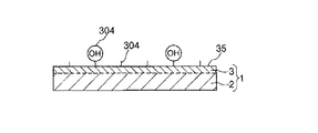
該基材上に、金属錯体を含有する液状材料を供給し、該液状材料を乾燥・焼成することにより設けられた、金属原子と、有機成分で構成される脱離基とを含む接合膜とを有し、
前記接合膜の少なくとも一部の領域にエネルギーを付与し、前記接合膜の表面付近に存在する前記脱離基が当該接合膜から脱離することにより、前記接合膜の表面の前記領域に、他の被着体との接着性が発現するものであることを特徴とする。
これにより、被着体に対して、高い寸法精度で強固に、かつ低温下で効率よく接合することができる接合膜を備えた接合膜付き基材が得られる。
Such an object is achieved by the present invention described below.
The substrate with a bonding film of the present invention comprises a substrate and
A bonding film comprising a metal atom and a leaving group composed of an organic component, which is provided by supplying a liquid material containing a metal complex onto the substrate and drying and baking the liquid material; Have
Energy is applied to at least a part of the bonding film, and the leaving group existing in the vicinity of the surface of the bonding film is detached from the bonding film. It is characterized in that it exhibits adhesiveness to the adherend.
Thereby, the base material with a bonding film provided with the bonding film which can be firmly bonded to the adherend with high dimensional accuracy and efficiently at a low temperature is obtained.
本発明の接合膜付き基材では、前記脱離基は、前記液状材料を乾燥させた後、焼成した際に、前記金属錯体に含まれる有機物の一部が残存したものであることが好ましい。
このように成膜した際に膜中に残存する残存物を脱離基として用いる構成とすることにより、形成された金属膜中に脱離基を導入する必要がなく、比較的簡単な工程で接合膜を成膜することができる。
In the base material with a bonding film of the present invention, the leaving group is preferably one in which a part of the organic matter contained in the metal complex remains when the liquid material is dried and then baked.
By adopting a structure in which the residue remaining in the film when the film is formed is used as the leaving group, it is not necessary to introduce the leaving group into the formed metal film, and the process is relatively simple. A bonding film can be formed.
本発明の接合膜付き基材では、前記焼成の際の焼成温度は、70〜300℃であることが好ましい。
かかる範囲内に設定することにより、金属錯体に含まれる有機物が、その一部を残存させた状態で、金属錯体中から確実に除去されるため、その表面にエネルギーを付与することにより接着性が好適に発現する接合膜を確実に形成することができる。
In the base material with a bonding film of the present invention, the firing temperature during the firing is preferably 70 to 300 ° C.
By setting within this range, the organic matter contained in the metal complex is reliably removed from the metal complex in a state in which a part of the organic substance remains, so that adhesion can be obtained by applying energy to the surface. A bonding film that is suitably expressed can be formed reliably.
本発明の接合膜付き基材では、前記焼成は、不活性ガス雰囲気下で行われることが好ましい。
これにより、基材上に純粋な金属膜が形成されることなく、金属錯体中に含まれる有機物の一部を残存させた状態で接合膜を形成することができる。その結果、接合膜および金属膜としての双方の特性に優れた接合膜を形成することができる。
In the base material with a bonding film of the present invention, the firing is preferably performed in an inert gas atmosphere.
As a result, the bonding film can be formed in a state in which a part of the organic substance contained in the metal complex is left without forming a pure metal film on the substrate. As a result, it is possible to form a bonding film having excellent characteristics as both the bonding film and the metal film.
本発明の接合膜付き基材では、前記焼成は、減圧下で行われることが好ましい。
これにより、形成される接合膜の膜密度が緻密化して、接合膜をより優れた膜強度を有するものとすることができる。
本発明の接合膜付き基材では、前記脱離基は、炭素原子を必須成分とし、水素原子、窒素原子、酸素原子、リン原子、硫黄原子およびハロゲン原子のうちの少なくとも1種を含む原子団で構成されることが好ましい。
これらの脱離基は、エネルギーの付与による結合/脱離の選択性に比較的優れている。このため、エネルギーを付与することによって比較的簡単に、かつ均一に脱離する脱離基が得られることとなり、接合膜付き基材の接着性をより高度化することができる。
In the base material with a bonding film of the present invention, the baking is preferably performed under reduced pressure.
Thereby, the film density of the formed bonding film is densified, and the bonding film can have more excellent film strength.
In the base material with a bonding film of the present invention, the leaving group is an atomic group containing a carbon atom as an essential component and containing at least one of a hydrogen atom, a nitrogen atom, an oxygen atom, a phosphorus atom, a sulfur atom and a halogen atom. It is preferable that it is comprised.
These leaving groups are relatively excellent in binding / leaving selectivity by applying energy. For this reason, the leaving group which leaves | separates comparatively easily and uniformly by providing energy will be obtained, and the adhesiveness of the base material with a bonding film can be further enhanced.
本発明の接合膜付き基材では、前記脱離基は、アルキル基を含むことが好ましい。
アルキル基で構成される脱離基は、化学的な安定性が高いため、脱離基としてアルキル基を備える接合膜は、耐候性および耐薬品性に優れたものとなる。
本発明の接合膜付き基材では、前記金属原子は、銅、アルミニウム、亜鉛、鉄およびルテニウムのうちの少なくとも1種であることが好ましい。
接合膜を、これらの金属原子を含むものとすることにより、接合膜は、優れた導電性を発揮するものとなる。
In the base material with a bonding film of the present invention, the leaving group preferably includes an alkyl group.
Since a leaving group composed of an alkyl group has high chemical stability, a bonding film having an alkyl group as the leaving group has excellent weather resistance and chemical resistance.
In the base material with a bonding film of the present invention, the metal atom is preferably at least one of copper, aluminum, zinc, iron and ruthenium.
By making the bonding film contain these metal atoms, the bonding film exhibits excellent conductivity.
本発明の接合膜付き基材では、前記接合膜中の金属原子と炭素原子との存在比は、3:7〜7:3であることが好ましい。
金属原子と炭素原子の存在比を前記範囲内になるよう設定することにより、接合膜の安定性が高くなり、接合膜付き基材と対向基板とをより強固に接合することができるようになる。また、接合膜を優れた導電性を発揮するものとすることができる。
In the base material with a bonding film of the present invention, the abundance ratio of metal atoms to carbon atoms in the bonding film is preferably 3: 7 to 7: 3.
By setting the abundance ratio of metal atoms and carbon atoms to be within the above range, the stability of the bonding film is increased, and the substrate with the bonding film and the counter substrate can be bonded more firmly. . In addition, the bonding film can exhibit excellent conductivity.
本発明の接合膜付き基材では、前記接合膜は、導電性を有することが好ましい。
これにより、本発明の接合膜付き基材を、他の被着体に対して接合した際に、接合膜を配線基板が備える配線や、その端子等に適用することができる。
本発明の接合膜付き基材では、前記接合膜は、その少なくとも表面付近に存在する前記脱離基が、当該接合膜から脱離した後に、活性手が生じることが好ましい。
これにより、他の被着体に対して、化学的結合に基づいて強固に接合可能な接合膜付き基材が得られる。
In the base material with a bonding film of the present invention, the bonding film preferably has conductivity.
Thereby, when the base material with a bonding film of the present invention is bonded to another adherend, the bonding film can be applied to a wiring provided in the wiring board, its terminals, and the like.
In the base material with a bonding film of the present invention, the bonding film preferably has an active hand after the leaving group existing at least near the surface thereof is released from the bonding film.
Thereby, the base material with a joining film which can be firmly joined to other adherends based on a chemical bond is obtained.
本発明の接合膜付き基材では、前記活性手は、未結合手または水酸基であることが好ましい。
これにより、他の被着体に対して、特に強固な接合が可能となる。
本発明の接合膜付き基材では、前記接合膜の平均厚さは、1〜1000nmであることが好ましい。
これにより、接合膜付き基材と他の被着体とを接合した接合体の寸法精度が著しく低下するのを防止しつつ、これらをより強固に接合することができる。
In the base material with a bonding film of the present invention, the active hand is preferably a dangling bond or a hydroxyl group.
Thereby, especially strong joining is possible with respect to other adherends.
In the base material with a bonding film of the present invention, the average thickness of the bonding film is preferably 1 to 1000 nm.
Thereby, these can be joined more firmly, preventing the dimensional accuracy of the joined body which joined the base material with a joining film, and another to-be-adhered body falling remarkably.
本発明の接合膜付き基材では、前記接合膜は、流動性を有さない固体状をなしていることが好ましい。
これにより、接合膜付き基材を用いて得られた接合体の寸法精度は、従来に比べて格段に高いものとなる。また、従来に比べ、短時間で強固な接合が可能になる。
本発明の接合膜付き基材では、前記基材は、板状をなしていることが好ましい。
これにより、基材が撓み易くなり、基材は、他の被着体の形状に沿って十分に変形可能なものとなるため、これらの密着性がより高くなる。また、基材が撓むことによって、接合界面に生じる応力を、ある程度緩和することができる。
In the base material with a bonding film of the present invention, the bonding film is preferably in a solid state having no fluidity.
Thereby, the dimensional accuracy of the joined body obtained using the base material with a joining film becomes remarkably high compared with the past. In addition, stronger bonding can be achieved in a shorter time than in the past.
In the base material with a bonding film of the present invention, the base material preferably has a plate shape.
Thereby, since a base material becomes easy to bend and a base material becomes a thing which can fully change along the shape of other adherends, these adhesiveness becomes higher. Moreover, the stress which arises in a joining interface by bending a base material can be relieved to some extent.
本発明の接合膜付き基材では、前記基材の少なくとも前記接合膜を形成する部分は、シリコン材料、金属材料またはガラス材料を主材料として構成されていることが好ましい。
これにより、表面処理を施さなくても、十分な接合強度が得られる。
本発明の接合膜付き基材では、前記基材の前記接合膜を備える面には、あらかじめ、前記接合膜との密着性を高める表面処理が施されていることが好ましい。
これにより、基材の表面を清浄化および活性化し、接合膜と対向基板との接合強度を高めることができる。
In the base material with a bonding film of the present invention, it is preferable that at least a portion of the base material forming the bonding film is composed mainly of a silicon material, a metal material, or a glass material.
Thereby, sufficient bonding strength can be obtained without surface treatment.
In the base material with a bonding film of the present invention, it is preferable that a surface of the base material provided with the bonding film is previously subjected to a surface treatment for improving adhesion with the bonding film.
Thereby, the surface of the base material can be cleaned and activated, and the bonding strength between the bonding film and the counter substrate can be increased.
本発明の接合膜付き基材では、前記表面処理は、プラズマ処理であることが好ましい。
これにより、接合膜を形成するために、基材の表面を特に最適化することができる。
本発明の接合膜付き基材では、前記基材と前記接合膜との間に、中間層が介挿されていることが好ましい。
これにより、信頼性の高い接合体を得ることができる。
本発明の接合膜付き基材では、前記中間層は、酸化物系材料を主材料として構成されていることが好ましい。
これにより、基材と接合膜との間の接合強度を特に高めることができる。
In the substrate with a bonding film of the present invention, the surface treatment is preferably a plasma treatment.
Thereby, in order to form a joining film | membrane, the surface of a base material can be optimized especially.
In the base material with a bonding film of the present invention, it is preferable that an intermediate layer is interposed between the base material and the bonding film.
Thereby, a highly reliable joined body can be obtained.
In the base material with a bonding film of the present invention, the intermediate layer is preferably composed of an oxide-based material as a main material.
Thereby, the joint strength between the base material and the joining film can be particularly increased.
本発明の接合方法は、本発明の接合膜付き基材と、前記他の被着体とを用意する工程と、
該接合膜付き基材中の前記接合膜の少なくとも一部の領域にエネルギーを付与する工程と、
前記接合膜と前記他の被着体とを密着させるように、前記接合膜付き基材と前記他の被着体とを貼り合わせ、接合体を得る工程とを有することを特徴とする。
これにより、接合膜付き基材と被着体とを、低温下で効率よく接合することができる。
The bonding method of the present invention includes a step of preparing the substrate with the bonding film of the present invention and the other adherend,
Applying energy to at least a partial region of the bonding film in the substrate with the bonding film;
And bonding the base material with the bonding film and the other adherend so that the bonding film and the other adherend are brought into close contact with each other.
Thereby, the base material with a bonding film and the adherend can be efficiently bonded at a low temperature.
本発明の接合方法は、本発明の接合膜付き基材と、前記他の被着体とを用意する工程と、
前記接合膜と前記他の被着体とを密着させるように、前記接合膜付き基材と前記他の被着体とを貼り合わせ、積層体を得る工程と、
該積層体中の前記接合膜の少なくとも一部の領域にエネルギーを付与することにより、前記接合膜付き基材と前記他の被着体とを接合し、接合体を得る工程とを有することを特徴とする。
これにより、接合膜付き基材と被着体とを、低温下で効率よく接合することができる。また、積層体の状態では、接合膜付き基材と被着体との間は接合されていないので、接合膜付き基材と被着体とを重ね合わせた後、これらの位置を容易に微調整することができる。その結果、接合膜の表面方向における位置精度を高めることができる。
The bonding method of the present invention includes a step of preparing the substrate with the bonding film of the present invention and the other adherend,
Bonding the base material with the bonding film and the other adherend so that the bonding film and the other adherend are adhered, and obtaining a laminate;
A step of bonding the base material with the bonding film and the other adherend to obtain a bonded body by applying energy to at least a part of the bonding film in the laminate. Features.
Thereby, the base material with a bonding film and the adherend can be efficiently bonded at a low temperature. Further, in the state of the laminated body, since the substrate with the bonding film and the adherend are not bonded, after the substrate with the bonding film and the adherend are overlapped, these positions can be easily changed. Can be adjusted. As a result, the positional accuracy in the surface direction of the bonding film can be increased.
本発明の接合方法では、前記エネルギーの付与は、前記接合膜にエネルギー線を照射する方法、前記接合膜を加熱する方法、および前記接合膜に圧縮力を付与する方法のうちの少なくとも1つの方法により行われることが好ましい。
これにより、接合膜に対して比較的簡単に効率よくエネルギーを付与することができる。
In the bonding method of the present invention, the energy is applied by at least one of a method of irradiating the bonding film with energy rays, a method of heating the bonding film, and a method of applying a compressive force to the bonding film. Is preferably carried out by
Thereby, energy can be imparted to the bonding film relatively easily and efficiently.
本発明の接合方法では、前記エネルギー線は、波長126〜300nmの紫外線であることが好ましい。
これにより、接合膜に付与されるエネルギー量が最適化されるので、接合膜中の脱離基を確実に脱離させることができる。その結果、接合膜の特性(機械的特性、化学的特性等)が低下するのを防止しつつ、接合膜に接着性を発現させることができる。
In the bonding method of the present invention, the energy beam is preferably ultraviolet light having a wavelength of 126 to 300 nm.
As a result, the amount of energy applied to the bonding film is optimized, so that the leaving group in the bonding film can be desorbed with certainty. As a result, the bonding film can exhibit adhesiveness while preventing the characteristics (mechanical characteristics, chemical characteristics, etc.) of the bonding film from deteriorating.
本発明の接合方法では、前記加熱の温度は、25〜200℃であることが好ましい。
これにより、接合体が熱によって変質・劣化するのを確実に防止しつつ、接合強度を確実に高めることができる。
本発明の接合方法では、前記圧縮力は、0.2〜10MPaであることが好ましい。
これにより、圧力が高すぎて基板や被着体に損傷等が生じるのを防止しつつ、接合体の接合強度を確実に高めることができる。
本発明の接合方法では、前記エネルギーの付与は、大気雰囲気中で行われることが好ましい。
これにより、雰囲気を制御することに手間やコストをかける必要がなくなり、エネルギーの付与をより簡単に行うことができる。
In the bonding method of the present invention, the heating temperature is preferably 25 to 200 ° C.
Thereby, it is possible to reliably increase the bonding strength while reliably preventing the bonded body from being deteriorated and deteriorated by heat.
In the joining method of the present invention, the compressive force is preferably 0.2 to 10 MPa.
Thereby, it is possible to reliably increase the bonding strength of the bonded body while preventing the substrate and the adherend from being damaged due to the pressure being too high.
In the bonding method of the present invention, it is preferable that the application of energy is performed in an air atmosphere.
Thereby, it is not necessary to spend time and cost to control the atmosphere, and energy can be applied more easily.
本発明の接合方法では、前記他の被着体は、あらかじめ、前記接合膜との密着性を高める表面処理を施した表面を有するものであり、
前記接合膜付き基材は、前記表面処理を施した表面に対して、前記接合膜が密着するようにして貼り合わされることが好ましい。
これにより、接合膜付き基材と被着体との接合強度をより高めることができる。
In the bonding method of the present invention, the other adherend has a surface that has been subjected in advance to a surface treatment that improves adhesion with the bonding film,
It is preferable that the base material with the bonding film is bonded so that the bonding film is in close contact with the surface subjected to the surface treatment.
Thereby, the joint strength of the base material with a bonding film and the adherend can be further increased.
本発明の接合方法では、前記他の被着体は、あらかじめ、官能基、ラジカル、開環分子、不飽和結合、ハロゲンおよび過酸化物からなる群から選択される少なくとも1つの基または物質を有する表面を有するものであり、
前記接合膜付き基材は、前記基または物質を有する表面に対して、前記接合膜が密着するようにして貼り合わされることが好ましい。
これにより、接合膜付き基材と被着体との接合強度を十分に高くすることができる。
In the bonding method of the present invention, the other adherend has in advance at least one group or substance selected from the group consisting of a functional group, a radical, a ring-opening molecule, an unsaturated bond, a halogen, and a peroxide. Has a surface,
The substrate with the bonding film is preferably bonded so that the bonding film is in close contact with the surface having the group or substance.
As a result, the bonding strength between the substrate with the bonding film and the adherend can be sufficiently increased.
本発明の接合方法では、さらに、前記接合体に対して、その接合強度を高める処理を行う工程を有することが好ましい。
これにより、接合体の接合強度のさらなる向上を図ることができる。
本発明の接合方法では、前記接合強度を高める処理を行う工程は、前記接合体にエネルギー線を照射する方法、前記接合体を加熱する方法、および前記接合体に圧縮力を付与する方法のうちの少なくとも1つの方法により行われることが好ましい。
これにより、接合体の接合強度のさらなる向上を容易に図ることができる。
The bonding method of the present invention preferably further includes a step of performing a process for increasing the bonding strength of the bonded body.
Thereby, the joint strength of the joined body can be further improved.
In the bonding method of the present invention, the step of performing the process of increasing the bonding strength includes a method of irradiating the bonded body with energy rays, a method of heating the bonded body, and a method of applying a compressive force to the bonded body. It is preferable to carry out by at least one method.
Thereby, the further improvement of the joining strength of a joined body can be aimed at easily.
本発明の接合体は、本発明の接合膜付き基材と、被着体とを有し、
これらを、前記接合膜を介して接合してなることを特徴とする。
これにより、接合膜付き基材と被着体とが高い寸法精度で強固に接合してなる信頼性の高い接合体が得られる。
本発明の接合体は、本発明の接合膜付き基材を2枚有し、
これらを、前記接合膜同士を対向させて接合してなることを特徴とする。
これにより、接合膜付き基材と被着体とが高い寸法精度で強固に接合してなる信頼性の高い接合体が得られる。
The joined body of the present invention has the base material with the joined film of the present invention and an adherend,
These are bonded through the bonding film.
As a result, a highly reliable bonded body is obtained in which the substrate with the bonding film and the adherend are firmly bonded with high dimensional accuracy.
The joined body of the present invention has two substrates with the joined film of the present invention,
These are formed by bonding the bonding films to face each other.
As a result, a highly reliable bonded body is obtained in which the substrate with the bonding film and the adherend are firmly bonded with high dimensional accuracy.
以下、本発明の接合膜付き基材、接合方法および接合体を、添付図面に示す好適実施形態に基づいて詳細に説明する。
本発明の接合膜付き基材は、基板(基材)と、この基板上に設けられた接合膜とを有しており、対向基板(他の被着体)に対して接合するのに用いられるものである。
この接合膜付き基材のうち、接合膜は、金属錯体を含有する液状材料を乾燥・焼成することに得られた、金属原子と、有機成分で構成される脱離基を含む有機金属膜である。
Hereinafter, the base material with a bonding film, the bonding method, and the bonded body of the present invention will be described in detail based on preferred embodiments shown in the accompanying drawings.
The base material with a bonding film of the present invention includes a substrate (base material) and a bonding film provided on the substrate, and is used for bonding to a counter substrate (another adherend). It is what
Among the substrates with the bonding film, the bonding film is an organic metal film containing a metal atom and a leaving group composed of an organic component, obtained by drying and baking a liquid material containing a metal complex. is there.
このような接合膜を有する接合膜付き基材は、接合膜の少なくとも一部の領域、すなわち、平面視における接合膜の全面または一部の領域に対して、エネルギーを付与することにより、前記接合膜の表面付近に存在する脱離基が、接合膜から脱離するものである。そして、この接合膜は、脱離基の脱離によって、その表面のエネルギーを付与した領域に、他の被着体との接着性が発現するという特徴を有するものである。
このような特徴を有する接合膜付き基材は、対向基板に対して、高い寸法精度で強固に、かつ低温下で効率よく接合可能なものである。そして、かかる接合膜付き基材を用いることにより、基板と対向基板とが強固に接合してなる信頼性の高い接合体が得られる。
The substrate with the bonding film having such a bonding film is formed by applying energy to at least a part of the bonding film, that is, the entire surface or a part of the bonding film in a plan view. A leaving group existing near the surface of the film is detached from the bonding film. The bonding film is characterized in that adhesiveness to other adherends is exhibited in a region to which energy of the surface is imparted by elimination of the leaving group.
The base material with the bonding film having such characteristics can be bonded to the counter substrate firmly with high dimensional accuracy and efficiently at a low temperature. By using such a base material with a bonding film, a highly reliable bonded body in which the substrate and the counter substrate are firmly bonded can be obtained.
<第1実施形態>
まず、本発明の接合膜付き基材、この接合膜付き基材と対向基板(他の被着体)とを接合する接合方法(本発明の接合方法)、および本発明の接合膜付き基材を備える接合体の各第1実施形態について説明する。
図1および図2は、本発明の接合膜付き基材を用いて、接合膜付き基材と対向基板とを接合する接合方法の第1実施形態を説明するための図(縦断面図)、図3は、本発明の接合膜付き基材が備える接合膜のエネルギー付与前の状態を示す部分拡大図、図4は、本発明の接合膜付き基材が備える接合膜のエネルギー付与後の状態を示す部分拡大図である。なお、以下の説明では、図1ないし図4中の上側を「上」、下側を「下」と言う。
<First Embodiment>
First, the base material with the bonding film of the present invention, the bonding method (the bonding method of the present invention) for bonding the base material with the bonding film and the counter substrate (other adherend), and the base material with the bonding film of the present invention 1st Embodiment of a conjugate | zygote provided with is described.
1 and 2 are views (longitudinal sectional views) for explaining a first embodiment of a bonding method for bonding a substrate with a bonding film and a counter substrate using the substrate with a bonding film of the present invention, FIG. 3 is a partially enlarged view showing a state before applying energy of the bonding film provided in the base material with bonding film of the present invention, and FIG. 4 shows a state after applying energy of the bonding film provided in the base material with bonding film of the present invention. FIG. In the following description, the upper side in FIGS. 1 to 4 is referred to as “upper” and the lower side is referred to as “lower”.
本実施形態にかかる接合方法は、本発明の接合膜付き基材を用意する工程と、接合膜付き基材の接合膜に対してエネルギーを付与して、接合膜中から脱離基を脱離させることにより、接合膜を活性化させる工程と、対向基板(他の被着体)を用意し、接合膜付き基材が備える接合膜と対向基板とが密着するように、これらを貼り合わせ、接合体を得る工程とを有する。
以下、本実施形態にかかる接合方法の各工程について順次説明する。
The bonding method according to the present embodiment includes a step of preparing the substrate with the bonding film of the present invention, and applying energy to the bonding film of the substrate with the bonding film to remove the leaving group from the bonding film. The step of activating the bonding film and preparing the counter substrate (other adherend), and bonding them so that the bonding film and the counter substrate provided in the substrate with the bonding film are in close contact, Obtaining a joined body.
Hereinafter, each process of the joining method concerning this embodiment is demonstrated one by one.
[1]まず、接合膜付き基材1(本発明の接合膜付き基材)を用意する。
接合膜付き基材1は、図1(a)に示すように、板状をなす基板(基材)2と、基板2上に設けられた接合膜3とを有している。
このうち、基板2は、接合膜3を支持する程度の剛性を有するものであれば、いかなる材料で構成されたものであってもよい。
[1] First, a
As shown in FIG. 1A, the base material with a
Of these, the
具体的には、基板2の構成材料は、ポリエチレン、ポリプロピレン、エチレン−プロピレン共重合体、エチレン−酢酸ビニル共重合体(EVA)等のポリオレフィン、環状ポリオレフィン、変性ポリオレフィン、ポリ塩化ビニル、ポリ塩化ビニリデン、ポリスチレン、ポリアミド、ポリイミド、ポリアミドイミド、ポリカーボネート、ポリ−(4−メチルペンテン−1)、アイオノマー、アクリル系樹脂、ポリメチルメタクリレート、アクリロニトリル−ブタジエン−スチレン共重合体(ABS樹脂)、アクリロニトリル−スチレン共重合体(AS樹脂)、ブタジエン−スチレン共重合体、ポリオキシメチレン、ポリビニルアルコール(PVA)、エチレン−ビニルアルコール共重合体(EVOH)、ポリエチレンテレフタレート(PET)、ポリエチレンナフタレート、ポリブチレンテレフタレート(PBT)、ポリシクロヘキサンテレフタレート(PCT)等のポリエステル、ポリエーテル、ポリエーテルケトン(PEK)、ポリエーテルエーテルケトン(PEEK)、ポリエーテルイミド、ポリアセタール(POM)、ポリフェニレンオキシド、変性ポリフェニレンオキシド、ポリサルフォン、ポリエーテルサルフォン、ポリフェニレンサルファイド、ポリアリレート、芳香族ポリエステル(液晶ポリマー)、ポリテトラフルオロエチレン、ポリフッ化ビニリデン、その他フッ素系樹脂、スチレン系、ポリオレフィン系、ポリ塩化ビニル系、ポリウレタン系、ポリエステル系、ポリアミド系、ポリブタジエン系、トランスポリイソプレン系、フッ素ゴム系、塩素化ポリエチレン系等の各種熱可塑性エラストマー、エポキシ樹脂、フェノール樹脂、ユリア樹脂、メラミン樹脂、アラミド系樹脂、不飽和ポリエステル、シリコーン樹脂、ポリウレタン等、またはこれらを主とする共重合体、ブレンド体、ポリマーアロイ等の樹脂系材料、Fe、Ni、Co、Cr、Mn、Zn、Pt、Au、Ag、Cu、Pd、Al、W、Ti、V、Mo、Nb、Zr、Pr、Nd、Smのような金属、またはこれらの金属を含む合金、炭素鋼、ステンレス鋼、インジウム錫酸化物(ITO)、ガリウムヒ素のような金属系材料、単結晶シリコン、多結晶シリコン、非晶質シリコンのようなシリコン系材料、ケイ酸ガラス(石英ガラス)、ケイ酸アルカリガラス、ソーダ石灰ガラス、カリ石灰ガラス、鉛(アルカリ)ガラス、バリウムガラス、ホウケイ酸ガラスのようなガラス系材料、アルミナ、ジルコニア、フェライト、窒化ケイ素、窒化アルミニウム、窒化ホウ素、窒化チタン、炭化ケイ素、炭化ホウ素、炭化チタン、炭化タングステンのようなセラミックス系材料、グラファイトのような炭素系材料、またはこれらの各材料の1種または2種以上を組み合わせた複合材料等が挙げられる。
Specifically, the constituent material of the
また、基板2は、その表面に、Niめっきのようなめっき処理、クロメート処理のような不働態化処理、または窒化処理等を施したものであってもよい。
また、基板(基材)2の形状は、接合膜3を支持する面を有するような形状であればよく、板状のものに限定されない。すなわち、基材の形状は、例えば、塊状(ブロック状)や、棒状等であってもよい。
Further, the surface of the
Further, the shape of the substrate (base material) 2 may be any shape that has a surface for supporting the
なお、本実施形態では、基板2が板状をなしていることから、基板2が撓み易くなり、基板2は、後述する対向基板4の形状に沿って十分に変形可能なものとなるため、これらの密着性がより高くなる。また、接合膜付き基材1において、基板2と接合膜3との密着性が高くなるとともに、基板2が撓むことによって、接合界面に生じる応力を、ある程度緩和することができる。
In the present embodiment, since the
この場合、基板2の平均厚さは、特に限定されないが、0.01〜10mm程度であるのが好ましく、0.1〜3mm程度であるのがより好ましい。なお、対向基板4の平均厚さも、前述した基板2の平均厚さと同様の範囲内であるのが好ましい。
一方、接合膜3は、基板2と後述する対向基板4との間に位置し、これらの基板2、4の接合を担うものである。
かかる接合膜3は、金属錯体を含有する液状材料を乾燥・焼成することにより得られるものであり、金属原子と、有機成分で構成させる脱離基303とを含むものである(図3参照。)。
In this case, the average thickness of the
On the other hand, the
Such a
本発明の接合膜付き基材は、主にこの接合膜3の構成に特徴を有する。なお、この接合膜3については、後に詳述する。
また、基板2の少なくとも接合膜3を形成すべき領域には、基板2の構成材料に応じて、接合膜3を形成する前に、あらかじめ、基板2と接合膜3との密着性を高める表面処理を施すのが好ましい。
The substrate with a bonding film of the present invention is mainly characterized by the structure of the
In addition, in at least a region where the
かかる表面処理としては、例えば、スパッタリング処理、ブラスト処理のような物理的表面処理、酸素プラズマ、窒素プラズマ等を用いたプラズマ処理、コロナ放電処理、エッチング処理、電子線照射処理、紫外線照射処理、オゾン暴露処理のような化学的表面処理、または、これらを組み合わせた処理等が挙げられる。このような処理を施すことにより、基板2の接合膜3を形成すべき領域を清浄化するとともに、該領域を活性化させることができる。これにより、接合膜3と対向基板4との接合強度を高めることができる。
Examples of the surface treatment include physical surface treatment such as sputtering treatment and blast treatment, plasma treatment using oxygen plasma, nitrogen plasma, etc., corona discharge treatment, etching treatment, electron beam irradiation treatment, ultraviolet irradiation treatment, ozone Examples include chemical surface treatment such as exposure treatment, or a combination of these. By performing such treatment, the region where the
また、これらの各表面処理の中でもプラズマ処理を用いることにより、接合膜3を形成するために、基板2の表面を特に最適化することができる。
なお、表面処理を施す基板2が、樹脂材料(高分子材料)で構成されている場合には、特に、コロナ放電処理、窒素プラズマ処理等が好適に用いられる。
また、基板2の構成材料によっては、上記のような表面処理を施さなくても、接合膜3の接合強度が十分に高くなるものがある。このような効果が得られる基板2の構成材料としては、例えば、前述したような各種金属系材料、各種シリコン系材料、各種ガラス系材料等を主材料とするものが挙げられる。
Further, by using plasma treatment among these surface treatments, the surface of the
In addition, when the board |
Further, depending on the constituent material of the
このような材料で構成された基板2は、その表面が酸化膜で覆われており、この酸化膜の表面には、比較的活性の高い水酸基が結合している。したがって、このような材料で構成された基板2を用いると、上記のような表面処理を施さなくても、接合膜付き基材1(結合膜3)と対向基板4とを強固に接合することができる。
なお、この場合、基板2の全体が上記のような材料で構成されていなくてもよく、少なくとも接合膜3を形成すべき領域の表面付近が上記のような材料で構成されていればよい。
また、表面処理に代えて、基板2の少なくとも接合膜3を形成すべき領域には、あらかじめ、中間層を形成するようにしてもよい。
The surface of the
In this case, the
Further, instead of the surface treatment, an intermediate layer may be formed in advance in at least the region where the
この中間層は、いかなる機能を有するものであってもよく、特に限定されるものではないが、例えば、接合膜3との密着性を高める機能、クッション性(緩衝機能)、応力集中を緩和する機能、接合膜3を成膜する際に接合膜3の膜成長を促進する機能(シード層)、接合膜3を保護する機能(バリア層)等を有するものが好ましい。このような中間層を介して基板2と接合膜3とを接合することになり、信頼性の高い接合体を得ることができる。
The intermediate layer may have any function and is not particularly limited. For example, the intermediate layer has a function of improving adhesion to the
かかる中間層の構成材料としては、例えば、アルミニウム、チタン、タングステン、銅およびその合金等の金属系材料、金属酸化物、金属窒化物、シリコン酸化物のような酸化物系材料、金属窒化物、シリコン窒化物のような窒化物系材料、グラファイト、ダイヤモンドライクカーボンのような炭素系材料、シランカップリング剤、チオール系化合物、金属アルコキシド、金属−ハロゲン化合物のような自己組織化膜材料、樹脂系接着剤、樹脂フィルム、樹脂コーティング材、各種ゴム材料、各種エラストマーのような樹脂系材料等が挙げられ、これらのうちの1種または2種以上を組み合わせて用いることができる。
また、これらの各種材料で構成された中間層の中でも、酸化物系材料で構成された中間層によれば、基板2と接合膜3との間の接合強度を特に高めることができる。
Examples of the constituent material of the intermediate layer include metal materials such as aluminum, titanium, tungsten, copper and alloys thereof, metal oxides, metal nitrides, oxide materials such as silicon oxides, metal nitrides, Nitride-based materials such as silicon nitride, carbon-based materials such as graphite and diamond-like carbon, silane coupling agents, thiol-based compounds, metal alkoxides, self-assembled film materials such as metal-halogen compounds, and resin-based materials Examples thereof include resin materials such as adhesives, resin films, resin coating materials, various rubber materials, and various elastomers, and one or more of these can be used in combination.
Further, among the intermediate layers formed of these various materials, the bonding strength between the
[2]次に、接合膜付き基材1の接合膜3の表面35に対してエネルギーを付与する。
ここで、接合膜3にエネルギーを付与すると、接合膜3では、図3および図4に示すように、脱離基303の結合手が切れて接合膜3の表面35付近から脱離し、脱離基303が脱離した後には、活性手が接合膜3の表面35付近に生じる。これにより、接合膜3の表面35に、対向基板4との接着性が発現する。
このような状態の接合膜付き基材1は、対向基板4と、化学的結合に基づいて強固に接合可能なものとなる。
[2] Next, energy is applied to the
Here, when energy is applied to the
The
ここで、接合膜3に付与するエネルギーは、いかなる方法を用いて付与されるものであってもよいが、例えば、接合膜3にエネルギー線を照射する方法、接合膜3を加熱する方法、接合膜3に圧縮力(物理的エネルギー)を付与する方法、接合膜3をプラズマに曝す(プラズマエネルギーを付与する)方法、接合膜3をオゾンガスに曝す(化学的エネルギーを付与する)方法等が挙げられる。中でも、本実施形態では、接合膜3にエネルギーを付与する方法として、特に、接合膜3にエネルギー線を照射する方法を用いるのが好ましい。かかる方法は、接合膜3に対して比較的簡単に効率よくエネルギーを付与することができるので、エネルギーを付与する方法として好適に用いられる。
このうち、エネルギー線としては、例えば、紫外線、レーザ光のような光、X線、γ線、電子線、イオンビームのような粒子線等や、またはこれらのエネルギー線を2種以上組み合わせたものが挙げられる。
Here, the energy applied to the
Among these, as energy rays, for example, light such as ultraviolet rays and laser beams, X-rays, γ rays, electron beams, particle beams such as ion beams, etc., or a combination of two or more of these energy rays Is mentioned.
これらのエネルギー線の中でも、特に、波長126〜300nm程度の紫外線を用いるのが好ましい(図1(b)参照)。かかる範囲内の紫外線によれば、付与されるエネルギー量が最適化されるので、接合膜3中の脱離基303を確実に脱離させることができる。これにより、接合膜3の特性(機械的特性、化学的特性等)が低下するのを防止しつつ、接合膜3に接着性を確実に発現させることができる。
Among these energy rays, it is particularly preferable to use ultraviolet rays having a wavelength of about 126 to 300 nm (see FIG. 1B). With the ultraviolet rays within such a range, the amount of energy applied is optimized, so that the leaving
また、紫外線によれば、広い範囲をムラなく短時間に処理することができるので、脱離基303の脱離を効率よく行わせることができる。さらに、紫外線には、例えば、UVランプ等の簡単な設備で発生させることができるという利点もある。
なお、紫外線の波長は、より好ましくは、126〜200nm程度とされる。
また、UVランプを用いる場合、その出力は、接合膜3の面積に応じて異なるが、1mW/cm2〜1W/cm2程度であるのが好ましく、5mW/cm2〜50mW/cm2程度であるのがより好ましい。なお、この場合、UVランプと接合膜3との離間距離は、1〜10mm程度とするのが好ましく、1〜5mm程度とするのがより好ましい。
In addition, since ultraviolet rays can be processed in a short time without unevenness, the leaving
The wavelength of the ultraviolet light is more preferably about 126 to 200 nm.
In the case of using the UV lamp, the output may vary depending on the area of the
また、紫外線を照射する時間は、接合膜3の表面35付近の脱離基303を脱離し得る程度の時間、すなわち、接合膜3に必要以上に紫外線が照射されない程度の時間とするのが好ましい。これにより、接合膜3が変質・劣化するのを効果的に防止することができる。具体的には、紫外線の光量、接合膜3の構成材料等に応じて若干異なるものの、0.5〜30分程度であるのが好ましく、1〜10分程度であるのがより好ましい。
また、紫外線は、時間的に連続して照射されてもよいが、間欠的(パルス状)に照射されてもよい。
The time for irradiating with ultraviolet rays is preferably set to a time that allows the leaving
Moreover, although an ultraviolet-ray may be irradiated continuously in time, you may irradiate intermittently (pulse form).
一方、レーザ光としては、例えば、エキシマレーザのようなパルス発振レーザ(パルスレーザ)、炭酸ガスレーザ、半導体レーザのような連続発振レーザ等が挙げられる。中でも、パルスレーザが好ましく用いられる。パルスレーザでは、接合膜3のレーザ光が照射された部分に経時的に熱が蓄積され難いので、蓄積された熱による接合膜3の変質・劣化を確実に防止することができる。すなわち、パルスレーザによれば、接合膜3の内部にまで蓄積された熱の影響がおよぶのを、防止することができる。
On the other hand, examples of the laser light include a pulsed laser (pulse laser) such as an excimer laser, a continuous wave laser such as a carbon dioxide laser, and a semiconductor laser. Among these, a pulse laser is preferably used. In the pulse laser, heat hardly accumulates with time in the portion of the
また、パルスレーザのパルス幅は、熱の影響を考慮した場合、できるだけ短い方が好ましい。具体的には、パルス幅が1ps(ピコ秒)以下であるのが好ましく、500fs(フェムト秒)以下であるのがより好ましい。パルス幅を前記範囲内にすれば、レーザ光照射に伴って接合膜3に生じる熱の影響を、的確に抑制することができる。なお、パルス幅が前記範囲内程度に小さいパルスレーザは、「フェムト秒レーザ」と呼ばれる。
また、レーザ光の波長は、特に限定されないが、例えば、200〜1200nm程度であるのが好ましく、400〜1000nm程度であるのがより好ましい。
また、レーザ光のピーク出力は、パルスレーザの場合、パルス幅によって異なるが、0.1〜10W程度であるのが好ましく、1〜5W程度であるのがより好ましい。
The pulse width of the pulse laser is preferably as short as possible in consideration of the influence of heat. Specifically, the pulse width is preferably 1 ps (picosecond) or less, and more preferably 500 fs (femtosecond) or less. If the pulse width is within the above range, the influence of heat generated in the
The wavelength of the laser light is not particularly limited, but is preferably about 200 to 1200 nm, and more preferably about 400 to 1000 nm.
In the case of a pulse laser, the peak output of the laser light varies depending on the pulse width, but is preferably about 0.1 to 10 W, and more preferably about 1 to 5 W.
さらに、パルスレーザの繰り返し周波数は、0.1〜100kHz程度であるのが好ましく、1〜10kHz程度であるのがより好ましい。パルスレーザの周波数を前記範囲内に設定することにより、レーザ光を照射した部分の温度が著しく上昇して、接合膜30に含まれる有機成分の一部が残存した状態で、脱離基303を接合膜3の表面35付近から確実に切断することができる。
Furthermore, the repetition frequency of the pulse laser is preferably about 0.1 to 100 kHz, and more preferably about 1 to 10 kHz. By setting the frequency of the pulse laser within the above range, the temperature of the portion irradiated with the laser light is remarkably increased, and the leaving
なお、このようなレーザ光の各種条件は、レーザ光を照射された部分の温度が、好ましくは常温(室温)〜600℃程度、より好ましくは200〜600℃程度、さらに好ましくは300〜400℃程度になるように適宜調整されるのが好ましい。これにより、レーザ光を照射した部分の温度が著しく上昇して、接合膜30に含まれる有機成分の一部が残存した状態で、脱離基303を接合膜3から確実に切断することができる。
また、接合膜3に照射するレーザ光は、その焦点を、接合膜3の表面35に合わせた状態で、この表面35に沿って走査されるようにするのが好ましい。これにより、レーザ光の照射によって発生した熱が、表面35付近に局所的に蓄積されることとなる。その結果、接合膜3の表面35に存在する脱離基303を選択的に脱離させることができる。
The various conditions of such laser light are such that the temperature of the portion irradiated with the laser light is preferably from room temperature (room temperature) to about 600 ° C., more preferably about 200 to 600 ° C., and even more preferably 300 to 400 ° C. It is preferable to adjust as appropriate. Thereby, the temperature of the portion irradiated with the laser beam is remarkably increased, and the leaving
In addition, it is preferable that the laser light applied to the
また、接合膜3に対するエネルギー線の照射は、いかなる雰囲気中で行うようにしてもよく、具体的には、大気、酸素のような酸化性ガス雰囲気、水素のような還元性ガス雰囲気、窒素、アルゴンのような不活性ガス雰囲気、またはこれらの雰囲気を減圧した減圧(真空)雰囲気等が挙げられるが、中でも、特に、大気雰囲気中で行うのが好ましい。これにより、雰囲気を制御することに手間やコストをかける必要がなくなり、エネルギー線の照射をより簡単に行うことができる。
The
このように、エネルギー線を照射する方法によれば、接合膜3の表面35付近に対して選択的にエネルギーを付与することが容易に行えるため、例えば、エネルギーの付与による基板2および接合膜3の変質・劣化を防止することができる。
また、エネルギー線を照射する方法によれば、付与するエネルギーの大きさを、精度よく簡単に調整することができる。このため、接合膜3から脱離する脱離基303の脱離量を調整することが可能となる。このように脱離基303の脱離量を調整することにより、接合膜付き基材1と対向基板4との間の接合強度を容易に制御することができる。
As described above, according to the method of irradiating energy rays, it is possible to easily apply energy selectively to the vicinity of the
Moreover, according to the method of irradiating energy rays, the magnitude of energy to be applied can be easily adjusted with high accuracy. For this reason, it becomes possible to adjust the desorption amount of the leaving
すなわち、脱離基303の脱離量を多くすることにより、接合膜3の表面35付近に、より多くの活性手が生じるため、接合膜3に発現する接着性をより高めることができる。一方、脱離基303の脱離量を少なくすることにより、接合膜3の表面35付近に生じる活性手を少なくし、接合膜3に発現する接着性を抑えることができる。
なお、付与するエネルギーの大きさを調整するためには、例えば、エネルギー線の種類、エネルギー線の出力、エネルギー線の照射時間等の条件を調整すればよい。
さらに、エネルギー線を照射する方法によれば、短時間で大きなエネルギーを付与することができるので、エネルギーの付与をより効率よく行うことができる。
That is, by increasing the amount of elimination of the leaving
In addition, in order to adjust the magnitude | size of the energy to provide, what is necessary is just to adjust conditions, such as the kind of energy beam, the output of an energy beam, the irradiation time of an energy beam.
Furthermore, according to the method of irradiating energy rays, a large amount of energy can be applied in a short time, so that the energy can be applied more efficiently.
ここで、エネルギーが付与される前の接合膜3は、図3に示すように、その表面35付近に脱離基303を有している。かかる接合膜3にエネルギーを付与する、脱離基303(図3では、メチル基)が接合膜3から脱離する。これにより、図4に示すように、接合膜3の表面35に活性手304が生じ、活性化される。その結果、接合膜3の表面に接着性が発現する。
Here, the
ここで、本明細書中において、接合膜3が「活性化された」状態とは、上述のように接合膜3の表面35および内部の脱離基303が脱離して、接合膜3の構成原子において終端化されていない結合手(以下、「未結合手」または「ダングリングボンド」とも言う。)が生じた状態の他、この未結合手が水酸基(OH基)によって終端化された状態、さらに、これらの状態が混在した状態を含めて、接合膜3が「活性化された」状態と言うこととする。
Here, in the present specification, the state in which the
したがって、活性手304とは、図4に示すように、未結合手(ダングリングボンド)、または未結合手が水酸基によって終端化されたもののことを言う。このような活性手304が存在するようにすれば、対向基板4に対して、特に強固な接合が可能となる。
なお、後者の状態(未結合手が水酸基によって終端化された状態)は、例えば、接合膜3に対して大気雰囲気中でエネルギー線を照射することにより、大気中の水分が未結合手を終端化することによって、容易に生成されることとなる。
Therefore, the
The latter state (state in which the dangling bond is terminated by a hydroxyl group) is, for example, that the moisture in the atmosphere terminates the dangling bond by irradiating the
また、本実施形態では、接合膜付き基材1と対向基板4とを貼り合わせる前に、あらかじめ、接合膜付き基材1の接合膜3に対してエネルギーを付与する場合について説明しているが、かかるエネルギーの付与は、接合膜付き基材1と対向基板4とを貼り合わせる(重ね合わせる)際、または貼り合わせた(重ね合わせた)後に行うようにしてもよい。なお、このような場合については、後述する第2実施形態において説明する。
Moreover, although this embodiment demonstrates the case where energy is previously provided with respect to the
[3]次に、対向基板(他の被着体)4を用意する。そして、図1(c)に示すように、活性化させた接合膜3と対向基板4とが密着するように、接合膜付き基材1と対向基板4とを貼り合わせる。これにより、前記工程[2]において、接合膜3が対向基板4に対する接着性が発現していることから、接合膜3と対向基板4とが化学的に結合することとなり、図2(d)に示すような接合体5が得られる。
[3] Next, a counter substrate (another adherend) 4 is prepared. Then, as shown in FIG. 1C, the base material with
このようにして得られた接合体5では、従来の接合方法で用いられていた接着剤のように、主にアンカー効果のような物理的結合に基づく接着ではなく、共有結合のような短時間で生じる強固な化学的結合に基づいて、接合膜付き基材1と対向基板4とが接合されている。このため、接合体5は短時間で形成することができ、かつ、極めて剥離し難く、接合ムラ等も生じ難いものとなる。
The bonded body 5 thus obtained is not bonded mainly based on a physical bond such as an anchor effect, but a short time such as a covalent bond, unlike the adhesive used in the conventional bonding method. The
また、このような接合膜付き基材1を用いて得られた接合体5を得る方法によれば、従来の固体接合のように、高温(例えば、700℃以上)での熱処理を必要としないことから、耐熱性の低い材料で構成された基板2および対向基板4をも、接合に供することができる。
また、接合膜3を介して基板2と対向基板4とを接合しているため、基板2や対向基板4の構成材料に制約がないという利点もある。
以上のことから、本発明によれば、基板2および対向基板4の各構成材料の選択の幅をそれぞれ広げることができる。
Moreover, according to the method of obtaining the joined body 5 obtained using such a
Further, since the
From the above, according to the present invention, the selection range of each constituent material of the
また、固体接合では、接合膜を介していないため、基板2と対向基板4との間の熱膨張率に大きな差がある場合、その差に基づく応力が接合界面に集中し易く、剥離等が生じるおそれがあったが、接合体(本発明の接合体)5では、接合膜3によって応力の集中が緩和され、剥離の発生を的確に抑制または防止することができる。
また、本実施形態では、接合に供される基板2および対向基板4のうち、一方のみ(本実施形態では、基板2)に接合膜3が設けられている。そのため、基板2上に接合膜3を形成する際に、接合膜3の形成方法によっては、基板2が比較的長時間にわたって高温下に曝されることになるが、本実施形態では、対向基板4は、高温下に曝されることはない。
Further, since solid bonding does not involve a bonding film, if there is a large difference in the coefficient of thermal expansion between the
In the present embodiment, the
したがって、例えば、対向基板4として、耐熱性が比較的低いものを選択した場合であっても、本実施形態にかかる方法によれば、接合膜付き基材1と対向基板4とを強固に接合することができる。したがって、対向基板4を構成する材料は、耐熱性をあまり考慮することなく、幅広い材料から選択することが可能になるという利点もある。
ここで、用意する対向基板4は、基板2と同様、いかなる材料で構成されたものであってもよい。
Therefore, for example, even when a substrate having relatively low heat resistance is selected as the counter substrate 4, according to the method according to the present embodiment, the
Here, the counter substrate 4 to be prepared may be made of any material, like the
具体的には、対向基板4は、基板2の構成材料と同様の材料で構成し得る。
また、対向基板4の形状も、基板2と同様、接合膜3が密着する面を有する形状であれば、特に限定されず、例えば、板状(層状)、塊状(ブロック状)、棒状等とされる。
ところで、対向基板4の構成材料は、基板2と異なっていても同じであっても良いが、基板2と対向基板4の各熱膨張率は、ほぼ等しいものを選択するのが好ましい。基板2と対向基板4の熱膨張率がほぼ等しければ、接合膜付き基材1と対向基板4とを貼り合せた際に、その接合界面に熱膨張に伴う応力が発生し難くなる。その結果、最終的に得られる接合体5において、剥離等の不具合が発生するのを確実に防止することができる。
Specifically, the counter substrate 4 can be made of the same material as that of the
Similarly to the
By the way, the constituent material of the counter substrate 4 may be the same as or different from that of the
また、後に詳述するが、基板2および対向基板4の各熱膨張率が互いに異なる場合であっても、接合膜付き基材1と対向基板4とを貼り合わせる際の条件を以下のように最適化するのが好ましい。これにより、接合膜付き基材1と対向基板4とを高い寸法精度で強固に接合することができる。
すなわち、基板2と対向基板4の熱膨張率が互いに異なっている場合には、できるだけ低温下で接合を行うのが好ましい。接合を低温下で行うことにより、接合界面に発生する熱応力のさらなる低減を図ることができる。
As will be described in detail later, even when the coefficients of thermal expansion of the
In other words, when the coefficients of thermal expansion of the
具体的には、基板2と対向基板4との熱膨張率の差にもよるが、基板2および対向基板4の温度が25〜50℃程度である状態下で、接合膜付き基材1と対向基板4とを貼り合わせるのが好ましく、25〜40℃程度である状態下で貼り合わせるのがより好ましい。このような温度範囲であれば、基板2と対向基板4との熱膨張率の差がある程度大きくても、接合界面に発生する熱応力を十分に低減することができる。その結果、接合体5における反りや剥離等の発生を確実に抑制または防止することができる。
Specifically, depending on the difference in thermal expansion coefficient between the
また、この場合、具体的な基板2と対向基板4との間の熱膨張係数の差が、5×10⁻⁵/K以上あるような場合には、上記のようにして、できるだけ低温下で接合を行うことが特に推奨される。
さらに、基板2と対向基板4は、互いに剛性が異なっているのが好ましい。これにより、接合膜付き基材1と対向基板4とをより強固に接合することができる。
Further, in this case, when the difference in thermal expansion coefficient between the
Further, it is preferable that the
また、基板2と対向基板4のうち、少なくとも一方の基板は、その構成材料が樹脂材料で構成されているのが好ましい。樹脂材料は、その柔軟性により、接合膜付き基材1と対向基板4とを接合した際に、その接合界面に発生する応力(例えば、熱膨張に伴う応力等)を緩和することができる。このため、接合界面が破壊し難くなり、結果的に、接合強度の高い接合体5を得ることができる。
Further, it is preferable that at least one of the
以上説明したような対向基板4の接合膜付き基材1との接合に供される領域には、基板2と同様に、対向基板4の構成材料に応じて、接合を行う前に、あらかじめ、対向基板4と接合膜3との密着性を高める表面処理を施すのが好ましい。これにより、接合膜付き基材1と対向基板4との接合強度をより高めることができる。
なお、表面処理としては、基板2に対して施す前述したような表面処理と同様の処理を適用することができる。
In the region to be used for the bonding of the counter substrate 4 to the
As the surface treatment, the same treatment as the above-described surface treatment performed on the
また、対向基板4の構成材料によっては、上記のような表面処理を施さなくても、接合膜付き基材1と対向基板4との接合強度が十分に高くなるものがある。このような効果が得られる対向基板4の構成材料には、前述した基板2の構成材料と同様のもの、すなわち、各種金属系材料、各種シリコン系材料、各種ガラス系材料等を用いることができる。
さらに、対向基板4の接合膜付き基材1との接合に供される領域に、以下の基や物質を有する場合には、上記のような表面処理を施さなくても、接合膜付き基材1と対向基板4との接合強度を十分に高くすることができる。
Further, depending on the constituent material of the counter substrate 4, the bonding strength between the
Furthermore, in the case where the region provided for bonding with the
このような基や物質としては、例えば、水素原子、水酸基、チオール基、カルボキシル基、アミノ基、ニトロ基、イミダゾール基のような官能基、ラジカル、開環分子、2重結合、3重結合のような不飽和結合、F、Cl、Br、Iのようなハロゲン、過酸化物からなる群から選択される少なくとも1つの基または物質が挙げられる。このような基または物質を有する表面は、接合膜付き基材1の接合膜3に対する接合強度のさらなる向上を実現し得るものとなる。
Examples of such groups and substances include functional groups such as hydrogen atoms, hydroxyl groups, thiol groups, carboxyl groups, amino groups, nitro groups, and imidazole groups, radicals, ring-opened molecules, double bonds, and triple bonds. And at least one group or substance selected from the group consisting of unsaturated bonds such as F, Cl, Br, I, and peroxides. The surface having such a group or substance can realize further improvement in the bonding strength of the
また、このようなものを有する表面が得られるように、上述したような各種表面処理を適宜選択して行うことにより、接合膜付き基材1と特に強固に接合可能な対向基板4が得られる。
また、表面処理に代えて、対向基板4の接合膜付き基材1との接合に供される領域には、あらかじめ、接合膜3との密着性を高める機能を有する中間層を形成しておくのが好ましい。これにより、かかる中間層を介して接合膜付き基材1と対向基板4とを接合することになり、より接合強度の高い接合体5が得られるようになる。
かかる中間層の構成材料には、前述の基板2に形成する中間層の構成材料と同様のものを用いることができる。
In addition, by appropriately selecting and performing various surface treatments as described above so that a surface having such a material can be obtained, the counter substrate 4 that can be particularly strongly bonded to the
Further, in place of the surface treatment, an intermediate layer having a function of improving the adhesion with the
As the constituent material of the intermediate layer, the same constituent material as that of the intermediate layer formed on the
ここで、本工程において、接合膜付き基材1と対向基板4とを接合するメカニズムについて説明する。
例えば、対向基板4の接合膜付き基材1との接合に供される領域に、水酸基が露出している場合を例に説明すると、本工程において、接合膜付き基材1の接合膜3と対向基板4とが接触するように、これらを貼り合わせたとき、接合膜付き基材1の接合膜3の表面35に存在する水酸基と、対向基板4の前記領域に存在する水酸基とが、水素結合によって互いに引き合い、水酸基同士の間に引力が発生する。この引力によって、接合膜付き基材1と対向基板4とが接合されると推察される。
Here, in this step, a mechanism for bonding the
For example, in the case where a hydroxyl group is exposed in a region provided for bonding to the
また、この水素結合によって互いに引き合う水酸基同士は、温度条件等によって、脱水縮合を伴って表面から切断される。その結果、接合膜付き基材1と対向基板4との接触界面では、水酸基が結合していた結合手同士が結合する。これにより、接合膜付き基材1と対向基板4とがより強固に接合されると推察される。
なお、前記工程[2]で活性化された接合膜3の表面は、その活性状態が経時的に緩和してしまう。このため、前記工程[2]の終了後、できるだけ早く本工程[3]を行うようにするのが好ましい。具体的には、前記工程[2]の終了後、60分以内に本工程[3]を行うようにするのが好ましく、5分以内に行うのがより好ましい。かかる時間内であれば、接合膜3の表面が十分な活性状態を維持しているので、本工程で接合膜付き基材1(接合膜3)と対向基板4とを貼り合わせたとき、これらの間に十分な接合強度を得ることができる。
Further, the hydroxyl groups attracting each other by the hydrogen bond are cleaved from the surface with dehydration condensation depending on the temperature condition or the like. As a result, at the contact interface between the
Note that the active state of the surface of the
換言すれば、活性化させる前の接合膜3は、金属錯体を含有する液状材料を乾燥・焼成することにより得られたものであり、金属原子と、有機成分で構成される脱離基303を含む接合膜であるため、化学的に比較的安定であり、耐候性に優れている。このため、活性化させる前の接合膜3は、長期にわたる保存に適したものとなる。したがって、そのような接合膜3を備えた基板2を多量に製造または購入して保存しておき、本工程の貼り合わせを行う直前に、必要な個数のみに前記工程[2]に記載したエネルギーの付与を行うようにすれば、接合体5の製造効率の観点から有効である。
以上のようにして、図2(d)に示す接合体(本発明の接合体)5を得ることができる。
In other words, the
As described above, the joined body (joined body of the present invention) 5 shown in FIG. 2D can be obtained.
なお、図2(d)では、接合膜付き基材1の接合膜3の全面を覆うように対向基板4を重ね合わせているが、これらの相対的な位置は、互いにずれていてもよい。すなわち、接合膜3から対向基板4がはみ出るように、接合膜付き基材1と対向基板4とが重ね合わされていてもよい。
このようにして得られた接合体5は、基板2と対向基板4との間の接合強度が5MPa(50kgf/cm2)以上であるのが好ましく、10MPa(100kgf/cm2)以上であるのがより好ましい。このような接合強度を有する接合体5は、その剥離を十分に防止し得るものとなる。そして、後述のように、接合体5を用いて、例えば液滴吐出ヘッドを構成した場合、耐久性に優れた液滴吐出ヘッドが得られる。また、本発明の接合膜付き基材1によれば、基板2と対向基板4とが上記のような大きな接合強度で接合された接合体5を効率よく作製することができる。
In addition, in FIG.2 (d), although the opposing board | substrate 4 is piled up so that the whole surface of the
The bonded body 5 obtained in this way preferably has a bonding strength between the
なお、従来のシリコン基板同士を直接接合するような固体接合では、接合に供される基板の表面を活性化させても、その活性状態は、大気中で数秒〜数十秒程度の極めて短時間しか維持することができなかった。このため、表面の活性化を行った後、接合する2つの基板を貼り合わせる等の作業に要する時間を、十分に確保することができないという問題があった。 In addition, in the conventional solid bonding where the silicon substrates are directly bonded to each other, even if the surface of the substrate used for bonding is activated, the active state is an extremely short time of about several seconds to several tens of seconds in the atmosphere. It could only be maintained. For this reason, there has been a problem that it is not possible to sufficiently secure the time required for operations such as bonding the two substrates to be bonded after the surface activation.
これに対し、本発明によれば、比較的長時間に亘って活性状態を維持することができる。このため、貼り合わせ作業に要する時間を十分に確保することができ、接合作業の効率化を高めることができる。なお、比較的長時間に亘って活性状態を維持し得ることは、有機成分で構成される脱離基303が脱離した活性化状態が安定化していることに起因しているものと推察される。
On the other hand, according to the present invention, the active state can be maintained for a relatively long time. For this reason, the time required for the bonding operation can be sufficiently secured, and the efficiency of the bonding operation can be increased. The fact that the active state can be maintained for a relatively long time is presumed to be due to the stabilization of the activated state in which the
なお、接合体5を得る際、または、接合体5を得た後に、この接合体5(接合膜付き基材1と対向基板4の積層体)に対して、必要に応じ、以下の3つの工程([4A]、[4B]および[4C])のうちの少なくとも1つの工程(接合体5の接合強度を高める工程)を行うようにしてもよい。これにより、接合体5の接合強度のさらなる向上を図ることができる。
In addition, when obtaining the joined body 5 or after obtaining the joined body 5, the following three cases are applied to the joined body 5 (laminated body of the
[4A] 図2(e)に示すように、得られた接合体5を、基板2と対向基板4とが互いに近づく方向に加圧する。
これにより、基板2の表面および対向基板4の表面に、それぞれ接合膜3の表面がより近接し、接合体5における接合強度をより高めることができる。
また、接合体5を加圧することにより、接合体5中の接合界面に残存していた隙間を押し潰して、接合面積をさらに広げることができる。これにより、接合体5における接合強度をさらに高めることができる。
[4A] As shown in FIG. 2E, the obtained bonded body 5 is pressed in a direction in which the
Thereby, the surface of the
Further, by pressurizing the bonded body 5, the gap remaining at the bonded interface in the bonded body 5 can be crushed and the bonded area can be further expanded. Thereby, the joint strength in the joined body 5 can be further increased.
このとき、接合体5を加圧する際の圧力は、接合体5が損傷を受けない程度の圧力で、できるだけ高い方が好ましい。これにより、この圧力に比例して接合体5における接合強度を高めることができる。
なお、この圧力は、基板2および対向基板4の各構成材料や各厚さ、接合装置等の条件に応じて、適宜調整すればよい。具体的には、基板2および対向基板4の各構成材料や各厚さ等に応じて若干異なるものの、0.2〜15MPa程度であるのが好ましく、5〜10MPa程度であるのがより好ましい。これにより、接合体5の接合強度を確実に高めることができる。なお、この圧力が前記上限値を上回っても構わないが、基板2および対向基板4の各構成材料によっては、基板2および対向基板4に損傷等が生じるおそれがある。
また、加圧する時間は、特に限定されないが、10秒〜30分程度であるのが好ましい。なお、加圧する時間は、加圧する際の圧力に応じて適宜変更すればよい。具体的には、接合体5を加圧する際の圧力が高いほど、加圧する時間を短くしても、接合強度の向上を図ることができる。
At this time, the pressure at the time of pressurizing the bonded body 5 is a pressure that does not damage the bonded body 5 and is preferably as high as possible. Thereby, the joint strength in the joined body 5 can be increased in proportion to the pressure.
In addition, what is necessary is just to adjust this pressure suitably according to conditions, such as each component material of each of the board |
The time for pressurization is not particularly limited, but is preferably about 10 seconds to 30 minutes. In addition, what is necessary is just to change suitably the time to pressurize according to the pressure at the time of pressurizing. Specifically, the higher the pressure at which the bonded body 5 is pressed, the more the bonding strength can be improved even if the pressing time is shortened.
[4B] 図2(e)に示すように、得られた接合体5を加熱する。
これにより、接合体5における接合強度をより高めることができる。
このとき、接合体5を加熱する際の温度は、室温より高く、接合体5の耐熱温度未満であれば、特に限定されないが、好ましくは25〜200℃程度とされ、より好ましくは70〜150℃程度とされる。かかる範囲の温度で加熱すれば、接合体5が熱によって変質・劣化するのを確実に防止しつつ、接合強度を確実に高めることができる。
[4B] As shown in FIG. 2E, the obtained bonded body 5 is heated.
Thereby, the joint strength in the joined body 5 can be further increased.
At this time, the temperature at which the joined body 5 is heated is not particularly limited as long as it is higher than room temperature and lower than the heat resistance temperature of the joined body 5, but is preferably about 25 to 200 ° C., more preferably 70 to 150. About ℃. Heating at a temperature in such a range can reliably increase the bonding strength while reliably preventing the bonded body 5 from being altered or deteriorated by heat.
また、加熱時間は、特に限定されないが、1〜30分程度であるのが好ましい。
また、前記工程[4A]、[4B]の双方を行う場合、これらを同時に行うのが好ましい。すなわち、図2(e)に示すように、接合体5を加圧しつつ、加熱するのが好ましい。これにより、加圧による効果と、加熱による効果とが相乗的に発揮され、接合体5の接合強度を特に高めることができる。
The heating time is not particularly limited, but is preferably about 1 to 30 minutes.
Moreover, when performing both said process [4A] and [4B], it is preferable to perform these simultaneously. That is, as shown in FIG. 2 (e), it is preferable to heat the bonded body 5 while pressing it. Thereby, the effect by pressurization and the effect by heating are exhibited synergistically, and the joint strength of the joined body 5 can be particularly increased.
[4C] 図2(f)に示すように、得られた接合体5に紫外線を照射する。
これにより、接合膜3と基板2および対向基板4との間に形成される化学結合を増加させ、基板2および対向基板4と接合膜3との間の接合強度をそれぞれ高めることができる。その結果、接合体5の接合強度を特に高めることができる。
このとき照射される紫外線の条件は、前記工程[2]に示した紫外線の条件と同等にすればよい。
[4C] As shown in FIG. 2F, the obtained bonded body 5 is irradiated with ultraviolet rays.
Thereby, the chemical bond formed between the
The conditions of the ultraviolet rays irradiated at this time may be equivalent to the conditions of the ultraviolet rays shown in the step [2].
また、本工程[4C]を行う場合、基板2および対向基板4のうち、いずれか一方が透光性を有していることが必要である。そして、透光性を有する基板側から、紫外線を照射することにより、接合膜3に対して確実に紫外線を照射することができる。
以上のような工程を行うことにより、接合体5における接合強度のさらなる向上を容易に図ることができる。
ここで、前述したように、本発明の接合膜付き基材は、接合膜3の構成に特徴を有している。以下、接合膜3について詳述する。
Moreover, when performing this process [4C], it is required for either one of the board |
By performing the steps as described above, it is possible to easily further improve the bonding strength of the bonded body 5.
Here, as described above, the substrate with a bonding film of the present invention is characterized by the structure of the
前述したように、接合膜3は、金属錯体を含有する液状材料を乾燥・焼成することにより得られるものであり、図3および図4に示すように、金属原子と、有機成分で構成される脱離基303を含むものである。このような接合膜3は、エネルギーが付与されると、脱離基303が接合膜3の少なくとも表面35付近から脱離し、図4に示すように、接合膜3の少なくとも表面35付近に、活性手304が生じるものである。そして、これにより、接合膜3の表面に接着性が発現する。かかる接着性が発現すると、接合膜3を備えた接合膜付き基材1は、対向基板4に対して、高い寸法精度で強固に効率よく接合可能なものとなる。
As described above, the
また、接合膜3は、金属錯体を含有する液状材料を乾燥・焼成することにより得られる、金属原子と、有機成分で構成される脱離基303とを含むもの、すなわち有機金属膜であることから、変形し難い強固な膜となる。このため、接合膜3自体が寸法精度の高いものとなり、最終的に得られる接合体5においても、寸法精度が高いものが得られる。
このような接合膜3は、流動性を有さない固体状をなすものである。このため、従来から用いられている、流動性を有する液状または粘液状(半固形状)の接着剤に比べて、接着層(接合膜3)の厚さや形状がほとんど変化しない。したがって、接合膜付き基材1を用いて得られた接合体5の寸法精度は、従来に比べて格段に高いものとなる。さらに、接着剤の硬化に要する時間が不要になるため、短時間で強固な接合が可能となる。
The
Such a
また、本発明では、接合膜3は、導電性を有するものであるのが好ましい。これにより、後述する接合体において、接合膜3を配線基板が備える配線や、その端子等に適用することができる。
以上のような接合膜3としての機能が好適に発揮されるように、金属原子および脱離基303が選択される。
In the present invention, it is preferable that the
The metal atom and the leaving
具体的には、金属原子としては、例えば、Sc、Ti、V、Cr、Mn、Fe、Co、Ni、Cu、Y、Zr、Nb、Mo、Tc、Ru、Rh、Pd、Ag、Hf、Ta、W、Re、Os、Ir、Pt、Au、各種ランタノイド元素、各種アクチノイド元素のような遷移金属元素、Li、Be、Na、Mg、Al、K、Ca、Zn、Ga、Rb、Sr、Cd、In、Sn、Sb、Cs、Ba、Tl、Pd、Bi、Poのような典型金属元素等が挙げられる。 Specifically, examples of the metal atom include Sc, Ti, V, Cr, Mn, Fe, Co, Ni, Cu, Y, Zr, Nb, Mo, Tc, Ru, Rh, Pd, Ag, Hf, Transition metal elements such as Ta, W, Re, Os, Ir, Pt, Au, various lanthanoid elements, various actinoid elements, Li, Be, Na, Mg, Al, K, Ca, Zn, Ga, Rb, Sr, Typical metal elements such as Cd, In, Sn, Sb, Cs, Ba, Tl, Pd, Bi, and Po are listed.
ここで、遷移金属元素は、各遷移金属元素間で、最外殻電子の数が異なることのみの差異であるため、物性が類似している。そして、遷移金属は、一般に、硬度や融点が高く、電気伝導性および熱伝導性が高い。このため、金属原子として遷移金属元素を用いた場合、接合膜3に発現する接着性をより高めることができる。また、それとともに、接合膜3の導電性をより高めることができる。
Here, since the transition metal element is the only difference in the number of outermost electrons between the transition metal elements, the physical properties are similar. Transition metals generally have high hardness and melting point, and high electrical conductivity and thermal conductivity. For this reason, when a transition metal element is used as a metal atom, the adhesiveness expressed in the
また、金属原子として、Cu、Al、Zn、FeおよびRuのうちの1種または2種以上を組み合わせて用いた場合、接合膜3は、優れた導電性を発揮するものとなる。また、金属錯体を含有する液状材料を乾燥・焼成して接合膜3を得る際に、これらの金属を含む金属錯体を原材料として用いて、比較的容易かつ均一な膜厚の接合膜3を成膜することができる。
Further, when one or more of Cu, Al, Zn, Fe, and Ru are used as metal atoms in combination, the
また、脱離基303は、前述したように、接合膜3から脱離することにより、接合膜3に活性手を生じさせるよう振る舞うものである。したがって、脱離基303には、エネルギーを付与されることによって、比較的簡単に、かつ均一に脱離するものの、エネルギーが付与されないときには、脱離しないよう接合膜3に確実に結合しているものが好適に選択される。
Further, as described above, the leaving
具体的には、脱離基303としては、炭素原子を必須成分とし、水素原子、窒素原子、酸素原子、リン原子、硫黄原子およびハロゲン原子のうちの少なくとも1種を含む原子団が好適に選択される。かかる脱離基303は、エネルギーの付与による結合/脱離の選択性に比較的優れている。このため、このような脱離基303は、上記のような必要性を十分に満足し得るものとなり、接合膜付き基材1の接着性をより高度なものとすることができる。
Specifically, as the leaving
より具体的には、原子団(基)としては、例えば、メチル基、エチル基のようなアルキル基、メトキシ基、エトキシ基のようなアルコキシ基、カルボキシル基の他、前記アルキル基の末端がイソシアネート基、アミノ基およびスルホン酸基等で終端しているもの等が挙げられる。
以上のような原子団の中でも、脱離基303は、特に、アルキル基を含むのが好ましい。アルキル基を含む脱離基303は、化学的な安定性が高いため、脱離基303としてアルキル基を備える接合膜3は、耐候性および耐薬品性に優れたものとなる。
More specifically, examples of the atomic group (group) include an alkyl group such as a methyl group and an ethyl group, an alkoxy group such as a methoxy group and an ethoxy group, and a carboxyl group, and the end of the alkyl group is an isocyanate group. And those terminated with a group, an amino group, a sulfonic acid group, and the like.
Among the atomic groups as described above, it is particularly preferable that the leaving
また、かかる構成の接合膜3において、金属原子と炭素原子の存在比は、3:7〜7:3程度であるのが好ましく、4:6〜6:4程度であるのがより好ましい。金属原子と炭素原子の存在比を前記範囲内になるよう設定することにより、接合膜3の安定性が高くなり、接合膜付き基材1と対向基板4とをより強固に接合することができるようになる。また、接合膜3を優れた導電性を発揮するものとすることができる。
In the
また、接合膜3の平均厚さは、1〜1000nm程度であるのが好ましく、50〜800nm程度であるのがより好ましい。接合膜3の平均厚さを前記範囲内とすることにより、接合膜付き基材1と対向基板4とを接合した接合体5の寸法精度が著しく低下するのを防止しつつ、これらをより強固に接合することができる。
すなわち、接合膜3の平均厚さが前記下限値を下回った場合は、十分な接合強度が得られないおそれがある。一方、接合膜3の平均厚さが前記上限値を上回った場合は、接合体5の寸法精度が著しく低下するおそれがある。
The average thickness of the
That is, when the average thickness of the
さらに、接合膜3の平均厚さが前記範囲内であれば、接合膜3にある程度の形状追従性が確保される。このため、例えば、基板2の接合面(接合膜3に隣接する面)に凹凸が存在している場合でも、その凹凸の高さにもよるが、凹凸の形状に追従するように接合膜3を被着させることができる。その結果、接合膜3は、凹凸を吸収して、その表面に生じる凹凸の高さを緩和することができる。そして、接合膜付き基材1と対向基板4とを貼り合わせた際に、接合膜3の対向基板4に対する密着性を高めることができる。
Furthermore, if the average thickness of the
なお、上記のような形状追従性の程度は、接合膜3の厚さが厚いほど顕著になる。したがって、形状追従性を十分に確保するためには、接合膜3の厚さをできるだけ厚くすればよい。
以上説明したような基板2上に設けられた接合膜3は、本発明では、基板2上に、金属錯体を含有する液状材料を供給し、この液状材料を乾燥・焼成することにより形成される。
以下、このような金属錯体を含有する液状材料を用いた接合膜3の形成方法について説明する。
Note that the degree of the shape followability as described above becomes more significant as the thickness of the
In the present invention, the
Hereinafter, a method for forming the
[1]まず、基板2を用意する。
この基板2としては、前述したような表面処理が施されたものや、その表面に中間層が形成されたものを用いるようにしてもよい。
[2]次に、金属錯体を含有する液状材料を、基板2上に供給し、この液状材料中に含まれる溶媒を除去し乾燥させることにより、基板2上に乾燥被膜を形成する。
液状材料を基板2上に供給する方法としては、特に限定されず、各種塗布法を用いることができ、例えば、スピンコート法、キャスティング法、マイクログラビアコート法、グラビアコート法、バーコート法、ロールコート法、ワイヤーバーコート法、ディップコート法、スプレーコート法、スクリーン印刷法、フレキソ印刷法、オフセット印刷法、マイクロコンタクトプリンティング法および液滴吐出法等が挙げられる。
[1] First, the
As the
[2] Next, a liquid material containing a metal complex is supplied onto the
A method for supplying the liquid material onto the
液状材料の粘度(25℃)は、通常、0.5〜200mPa・s程度であるのが好ましく、3〜100mPa・s程度であるのがより好ましい。液状材料の粘度をかかる範囲とすることにより、基板2上に液状材料を確実に供給することができる。さらに、この液状材料を乾燥・焼成させた際に、接合膜3を形成するのに十分な量の金属錯体を液状材料中に含有したものとすることができる。
また、上記の塗布法の中でも、特に、液滴吐出法を用いるのが好ましい。液滴吐出法によれば、液状材料を液滴として基板2の表面に供給することができるため、たとえ液状材料を基板2上の一部の領域に選択的に供給する場合であったとしても、液状材料をこの領域の形状に対応して確実に供給することができる。
In general, the viscosity (25 ° C.) of the liquid material is preferably about 0.5 to 200 mPa · s, and more preferably about 3 to 100 mPa · s. By setting the viscosity of the liquid material in such a range, the liquid material can be reliably supplied onto the
Of the above-described coating methods, it is particularly preferable to use a droplet discharge method. According to the droplet discharge method, the liquid material can be supplied to the surface of the
液滴吐出法としては、特に限定されないが、圧電素子による振動を利用して液状材料を吐出する構成のインクジェット法が好適に用いられる。インクジェット法によれば、目的とする領域(位置)に、液状材料を液滴として、優れた位置精度で供給することができる。また、圧電素子の振動数および液状材料の粘度等を適宜設定することにより、液滴のサイズ(大きさ)を、比較的容易に調整できることから、液滴のサイズを小さくすれば、たとえ接合膜3を形成する領域の形状が微細なものであったとしても、この領域の形状に対応して液状材料を供給することができる。 The droplet discharge method is not particularly limited, but an ink jet method in which a liquid material is discharged using vibration by a piezoelectric element is preferably used. According to the ink jet method, a liquid material can be supplied as droplets to a target region (position) with excellent positional accuracy. In addition, since the size (size) of the droplet can be adjusted relatively easily by appropriately setting the frequency of the piezoelectric element, the viscosity of the liquid material, and the like, even if the size of the droplet is reduced, the bonding film Even if the shape of the region forming 3 is fine, the liquid material can be supplied corresponding to the shape of this region.
塗布法として液滴吐出法を用いる場合、液状材料の粘度(25℃)は、3〜10mPa・s程度であるのが好ましく、4〜8mPa・s程度であるのがより好ましい。液状材料の粘度をかかる範囲とすることにより、液滴の吐出をより安定的に行うことができるとともに、微細な形状の接合膜3を形成する領域に対応した形状を描画し得る大きさの液滴を吐出することができる。
When the droplet discharge method is used as the coating method, the viscosity (25 ° C.) of the liquid material is preferably about 3 to 10 mPa · s, and more preferably about 4 to 8 mPa · s. By setting the viscosity of the liquid material in such a range, the liquid can be discharged more stably and can be drawn in a shape corresponding to the region where the
また、液状材料の粘度をかかる範囲内とすれば、具体的には、液滴31の量(液状材料の1滴の量)を、平均で、0.1〜40pL程度に、より現実的には1〜30pL程度に設定し得る。これにより、基板2上に供給された際の液滴の着弾径が小さなものとなることから、微細な形状の接合膜3をも確実に形成することができる。
さらに、基板2に供給する液滴31の供給量を適宜設定することにより、形成される接合膜3の厚さの制御を比較的容易に行うことができる。
液状材料は、前述のように金属錯体を含有し、この金属錯体を材料中に溶解または分散するための溶媒または分散剤を含有するものである。
Further, if the viscosity of the liquid material is within such a range, specifically, the amount of the droplets 31 (the amount of one droplet of the liquid material) is more realistically about 0.1 to 40 pL on average. Can be set to about 1 to 30 pL. Thereby, since the landing diameter of the droplet when supplied onto the
Furthermore, the thickness of the
The liquid material contains a metal complex as described above, and contains a solvent or a dispersant for dissolving or dispersing the metal complex in the material.
金属錯体を溶解または分散するための溶媒または分散媒としては、特に限定されず、例えば、アンモニア、水、過酸化水素、四塩化炭素、エチレンカーボネイト等の無機溶媒や、メチルエチルケトン(MEK)、アセトン等のケトン系溶媒、メタノール、エタノール、イソブタノール等のアルコール系溶媒、ジエチルエーテル、ジイソプロピルエーテル等のエーテル系溶媒、ブチルアミン、ドデシルアミンのようなアミン系溶媒、メチルセロソルブ等のセロソルブ系溶媒、ヘキサン、ペンタン等の脂肪族炭化水素系溶媒、トルエン、キシレン、ベンゼン等の芳香族炭化水素系溶媒、ピリジン、ピラジン、フラン等の芳香族複素環化合物系溶媒、N,N−ジメチルホルムアミド(DMF)等のアミド系溶媒、ジクロロメタン、クロロホルム等のハロゲン化合物系溶媒、酢酸エチル、酢酸メチル等のエステル系溶媒、ジメチルスルホキシド(DMSO)、スルホラン等の硫黄化合物系溶媒、アセトニトリル、プロピオニトリル、アクリロニトリル等のニトリル系溶媒、ギ酸、トリフルオロ酢酸等の有機酸系溶媒のような各種有機溶媒、または、これらを含む混合溶媒等を用いることができる。
金属錯体は、液状材料中に含まれ、本工程において、この液状材料を乾燥させることにより形成される乾燥被膜の主材料として構成する。
The solvent or dispersion medium for dissolving or dispersing the metal complex is not particularly limited, and examples thereof include inorganic solvents such as ammonia, water, hydrogen peroxide, carbon tetrachloride, and ethylene carbonate, methyl ethyl ketone (MEK), acetone, and the like. Ketone solvents, alcohol solvents such as methanol, ethanol, isobutanol, ether solvents such as diethyl ether and diisopropyl ether, amine solvents such as butylamine and dodecylamine, cellosolve solvents such as methyl cellosolve, hexane, pentane Aliphatic hydrocarbon solvents such as toluene, xylene and benzene, aromatic heterocyclic solvents such as pyridine, pyrazine and furan, amides such as N, N-dimethylformamide (DMF) Solvents, dichloromethane, chloroform, etc. Rogen compound solvents, ester solvents such as ethyl acetate and methyl acetate, sulfur compound solvents such as dimethyl sulfoxide (DMSO) and sulfolane, nitrile solvents such as acetonitrile, propionitrile and acrylonitrile, formic acid and trifluoroacetic acid Various organic solvents such as organic acid solvents, mixed solvents containing these, and the like can be used.
The metal complex is contained in a liquid material, and is configured as a main material of a dry film formed by drying the liquid material in this step.
この金属錯体としては、形成すべき接合膜3の種類に応じて適宜選択され、特に限定されるものではないが、例えば、ビス(2,6−ジメチル−2−(トリメチルシリロキシ)−3,5−ヘプタジオナト)銅(II)(Cu(SOPD)2;C24H46CuO6Si2)、2,4−ペンタジオネート−銅(II)、Cu(ヘキサフルオロアセチルアセトネート)(ビニルトリメチルシラン)[Cu(hfac)(VTMS)]、Cu(ヘキサフルオロアセチルアセトネート)(2−メチル−1−ヘキセン−3−エン)[Cu(hfac)(MHY)]、Cu(パーフルオロアセチルアセトネート)(ビニルトリメチルシラン)[Cu(pfac)(VTMS)]、Cu(パーフルオロアセチルアセトネート)(2−メチル−1−ヘキセン−3−エン)[Cu(pfac)(MHY)]、ビス(ジピバロイルメタナイト)銅[Cu(DPM)2、DMP:C11H19O2]、トリス(ジピバロイルメタナイト)イリジウム[Ir(DPM)3]、トリス(ジピバロイルメタナイト)イットリウム[Y(DPM)3]、トリス(ジピバロイルメタナイト)ガドリニウム[Gd(DPM)3]、ビス(イソブチルピバロイルメタナイト)銅[Cu(IBPM)2、IBMP:C10H17O2]トリス(イソブチルピバロイルメタナイト)ルテニウム[Ru(IBPM)3]、ビス(ジイソブチリルメタナイト)銅[Cu(DIBM)2、DIBM:C9H15O2]のようなβジケトン系錯体、トリス(8−キノリノラト)アルミニウム(Alq3)、トリス(4−メチル−8キノリノレート)アルミニウム(III)(Almq3)、(8−ヒドロキシキノリン)亜鉛(Znq2)のようなキノリノール系錯体、銅フタロシアニンのようなフタロシアニン系錯体、トリフルオロ酢酸銅、トリフルオロ酢酸イットリウム、テレフタル酸銅錯体のようなカルボン酸塩系錯体および下記一般式(1)で表わされるギ酸銅錯体等が挙げられる。これらの中でも、βジケトン系錯体を用いるのが好ましい。βジケトン系錯体は、比較的各種溶媒に対して高い溶解性を示すものが多いので、βジケトン系錯体および溶媒の組み合わせを適宜選択することにより、目的とする膜厚を有する接合膜3を形成するのに十分な量のβジケトン系錯体を溶媒中に溶解させることができる。
This metal complex is appropriately selected according to the type of the
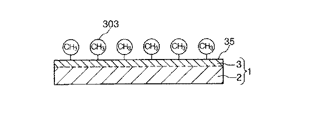
なお、一般式(1)中のR1およびR2のそれぞれの脂肪族炭化水素基は、飽和の脂肪族炭化水素基または不飽和の脂肪族炭化水素基が挙げられる。
飽和の脂肪族炭化水素基としては、アルキル基が挙げられる。例えば、アルキル基として、ブチル基、ヘキシル基、オクチル基、デシル基、ドデシル基、ヘキサデシル基、ノナデシル基などの直鎖アルキル基、イソブチル基、1−メチルヘキシル基、1−メチルオクチル基、1−メチルデシル基、1−メチルドデシル基、1−エチルドデシル基、1−メチルヘキサデシル基、1−メチルノナデシル基、tert−ブチル基、1,1−ジメチルヘキシル基、1,1−ジメチルオクチル基、1,1−ジメチルデシル基、1,1−ジメチルドデシル基、1,1−ジメチルヘキサデシル基、1,1−ジメチルノナデシル基などの分岐アルキル基が挙げられる。
In addition, as for each aliphatic hydrocarbon group of R < 1 > and R < 2 > in General formula (1), a saturated aliphatic hydrocarbon group or an unsaturated aliphatic hydrocarbon group is mentioned.
Examples of the saturated aliphatic hydrocarbon group include an alkyl group. For example, as an alkyl group, a butyl group, a hexyl group, an octyl group, a decyl group, a dodecyl group, a hexadecyl group, a nonadecyl group or the like linear alkyl group, an isobutyl group, a 1-methylhexyl group, a 1-methyloctyl group, 1- Methyldecyl group, 1-methyldodecyl group, 1-ethyldodecyl group, 1-methylhexadecyl group, 1-methylnonadecyl group, tert-butyl group, 1,1-dimethylhexyl group, 1,1-dimethyloctyl group, 1, Examples thereof include branched alkyl groups such as 1-dimethyldecyl group, 1,1-dimethyldodecyl group, 1,1-dimethylhexadecyl group and 1,1-dimethylnonadecyl group.
不飽和の脂肪族炭化水素基としては、アルケニル基またはアルキニル基が挙げられる。 例えば、アルケニル基として、1−ブテニル基、1−ヘキセニル基、1−オクテニル基、1−デセニル基、1−ドデセニル基、1−ヘキサデセニル基、1−ノナデセニル基などの直鎖アルケニル基、イソブテニル基、1−メチル−1−ヘキセニル基、1−メチル−1−オクテニル基、1−メチル−1−デセニル基、1−メチル−1−ドデセニル基、1−メチル−1−ヘキサデセニル基、sec−ブテニル基、1,1−ジメチル−2−ヘキセニル基、1,1−ジメチル−3−オクテニル基、1,1−ジメチル−4−デセニル基、1,1−ジメチル−5−ドデセニル基、1,1−ジメチル−6−ヘキサデセニル基などの分岐アルケニル基が挙げられる。 Examples of the unsaturated aliphatic hydrocarbon group include an alkenyl group and an alkynyl group. For example, as an alkenyl group, a linear alkenyl group such as 1-butenyl group, 1-hexenyl group, 1-octenyl group, 1-decenyl group, 1-dodecenyl group, 1-hexadecenyl group, 1-nonadecenyl group, isobutenyl group, 1-methyl-1-hexenyl group, 1-methyl-1-octenyl group, 1-methyl-1-decenyl group, 1-methyl-1-dodecenyl group, 1-methyl-1-hexadecenyl group, sec-butenyl group, 1,1-dimethyl-2-hexenyl group, 1,1-dimethyl-3-octenyl group, 1,1-dimethyl-4-decenyl group, 1,1-dimethyl-5-dodecenyl group, 1,1-dimethyl- Examples include branched alkenyl groups such as 6-hexadecenyl group.
例えば、アルキニル基として、2−ブチニル基、2−ヘキシニル基、2−オクチニル基、2−デシニル基、2−ドデシニル基、2−ヘキサデシニル基、2−ノナデシニル基などの直鎖アルキニル基、イソブチニル基、1−メチル−2−ヘキシニル基、1−メチル−2−オクチニル基、1−メチル−2−デシニル基、1−メチル−2−ドデシニル基、1−メチル−2−ヘキサデシニル基、1,1−ジメチル−2−ヘキシニル基、1,1−ジメチル−3−オクチニル基、1,1−ジメチル−4−デシニル基、1,1−ジメチル−5−ドデシニル基、1,1−ジメチル−6−ヘキサデシニル基などの分岐アルキニル基などが挙げられる。 For example, as the alkynyl group, a linear alkynyl group such as a 2-butynyl group, a 2-hexynyl group, a 2-octynyl group, a 2-decynyl group, a 2-dodecynyl group, a 2-hexadecynyl group, a 2-nonadecynyl group, an isobutynyl group, 1-methyl-2-hexynyl group, 1-methyl-2-octynyl group, 1-methyl-2-decynyl group, 1-methyl-2-dodecynyl group, 1-methyl-2-hexadecynyl group, 1,1-dimethyl 2-hexynyl group, 1,1-dimethyl-3-octynyl group, 1,1-dimethyl-4-decynyl group, 1,1-dimethyl-5-dodecynyl group, 1,1-dimethyl-6-hexadecynyl group, etc. And a branched alkynyl group.
上記のような金属錯体を用いることにより、次工程[3]において、乾燥被膜を焼成して接合膜3を形成する際に、金属錯体中に含まれる有機物を、その一部を接合膜3中に残存させつつ、金属錯体中から除去する(脱離させる)ことができる。
また、液状材料を乾燥させる際の温度は、金属錯体の種類、および、液状材料に含まれる溶媒または分散剤の種類によっても若干異なるが、25〜100℃程度であるのが好ましく、25〜75℃程度であるのがより好ましい。
By using the metal complex as described above, when forming the
In addition, the temperature at which the liquid material is dried slightly varies depending on the type of the metal complex and the type of the solvent or dispersant contained in the liquid material, but is preferably about 25 to 100 ° C. It is more preferable that the temperature is about ° C.
液状材料を乾燥させる時間は、0.5〜48時間程度であるのが好ましく、15〜30時間程度であるのがより好ましい。
さらに、液状材料を乾燥させる際の雰囲気の圧力は、大気圧下であってもよいが、減圧下であるのがより好ましい。減圧雰囲気下とする場合、減圧の程度は、1×10⁻⁷〜1×10⁻⁴Torr程度であるのが好ましく、1×10⁻⁶〜1×10⁻⁵Torr程度であるのがより好ましい。
液状材料を乾燥させる際の条件を上記のように設定することにより、液状材料中から溶媒または分散媒を除去して、主として金属錯体で構成される乾燥被膜を基板2上に確実に形成することができる。
The time for drying the liquid material is preferably about 0.5 to 48 hours, more preferably about 15 to 30 hours.
Furthermore, the pressure of the atmosphere when drying the liquid material may be under atmospheric pressure, but more preferably under reduced pressure. In the case of a reduced pressure atmosphere, the degree of pressure reduction is preferably about 1 × 10 −7 to 1 × 10 −4 Torr, and more preferably about 1 × 10 −6 to 1 × 10 −5 Torr. .
By setting the conditions for drying the liquid material as described above, the solvent or dispersion medium is removed from the liquid material, and a dry film mainly composed of a metal complex is reliably formed on the
[3]次に、基板2上に設けられた乾燥被膜を焼成する。
これにより、乾燥被膜中の金属錯体に含まれる有機物が、その一部を残存させた状態で、金属錯体中から除去される。その結果、基板2上に、金属原子と、有機成分で構成される脱離基とを含む接合膜3が形成される。
このように金属錯体を含む乾燥被膜を焼成して接合膜3を得る方法では、乾燥被膜を焼成した際に、接合膜3中で残存している前記有機物の一部が脱離基303として機能する。このように、本発明では、接合膜3を成膜する際に膜中に残存する有機物の一部(残存物)を脱離基303として用いる構成となっているので、形成した金属膜等に脱離基を導入する必要がなく、金属錯体を含有する液状材料を乾燥・焼成するという比較的簡単な工程で接合膜3を成膜することができる。
[3] Next, the dry film provided on the
Thereby, the organic substance contained in the metal complex in the dry film is removed from the metal complex in a state in which a part thereof remains. As a result, the
Thus, in the method of obtaining the
なお、金属錯体を用いて形成された接合膜3に残存する前記有機物の一部は、その全てが脱離基303として機能するものであってもよいし、その一部が脱離基303として機能するものであってもよい。
また、乾燥被膜を焼成する際の温度は、金属錯体の種類によっても若干異なるが、70〜300℃程度であるのが好ましく、100〜150℃程度であるのがより好ましい。
Note that part of the organic substance remaining in the
Moreover, although the temperature at the time of baking a dry film changes a little also with the kind of metal complex, it is preferable that it is about 70-300 degreeC, and it is more preferable that it is about 100-150 degreeC.
乾燥被膜を焼成する時間は、0.5〜48時間程度であるのが好ましく、15〜30時間程度であるのがより好ましい。
かかる条件で乾燥被膜を焼成することにより、金属錯体に含まれる有機物が、その一部を残存させた状態で、金属錯体中から確実に除去されるため、その表面にエネルギーを付与することにより接着性が好適に発現する接合膜3を確実に形成することができる。
The time for firing the dry film is preferably about 0.5 to 48 hours, more preferably about 15 to 30 hours.
By firing the dry film under such conditions, the organic matter contained in the metal complex is reliably removed from the metal complex in a state in which a portion of the organic substance remains, so that adhesion is achieved by applying energy to the surface. It is possible to reliably form the
さらに、乾燥被膜を焼成する際の雰囲気の圧力は、大気圧下であってもよいが、減圧下であるのがより好ましい。減圧雰囲気下とする場合、減圧の程度は、1×10⁻⁷〜1×10⁻⁴Torr程度であるのが好ましく、1×10⁻⁶〜1×10⁻⁵Torr程度であるのがより好ましい。これにより、接合膜3の膜密度が緻密化して、接合膜3をより優れた膜強度を有するものとすることができる。
Furthermore, the pressure of the atmosphere when firing the dry film may be under atmospheric pressure, but is more preferably under reduced pressure. In the case of a reduced pressure atmosphere, the degree of pressure reduction is preferably about 1 × 10 −7 to 1 × 10 −4 Torr, and more preferably about 1 × 10 −6 to 1 × 10 −5 Torr. . Thereby, the film density of the
また、乾燥被膜を焼成する際の雰囲気は、特に限定されないが、窒素、アルゴン、ヘリウムのような不活性ガス雰囲気であるのが好ましい。これにより、金属錯体中に含まれる有機物のほぼ全てが除去されることなく、すなわち、基板2上に純粋な金属膜が形成されることなく、金属錯体中に含まれる有機物の一部を残存させた状態で接合膜3を形成することができる。その結果、接合膜および金属膜としての双方の特性に優れた接合膜3を形成することができる。
Moreover, the atmosphere at the time of baking a dry film is although it does not specifically limit, It is preferable that it is inert gas atmosphere like nitrogen, argon, and helium. As a result, almost all of the organic matter contained in the metal complex is not removed, that is, a pure metal film is not formed on the
なお、金属錯体として、2,4−ペンタジオネート−銅(II)や[Cu(hfac)(VTMS)]等のように分子構造中に酸素原子を含有するものを用いる場合には、雰囲気中に、水素ガスを添加するのが好ましい。これにより、酸素原子に対する還元性を向上させることができ、接合膜3に過度の酸素原子が残存することなく、接合膜3を成膜することができる。その結果、この接合膜3は、膜中における金属酸化物の存在率が低いものとなり、優れた導電性を発揮することとなる。
When a metal complex containing an oxygen atom in its molecular structure such as 2,4-pentadionate-copper (II) or [Cu (hfac) (VTMS)] is used in the atmosphere It is preferable to add hydrogen gas. Thereby, the reducibility with respect to oxygen atoms can be improved, and the
また、乾燥被膜中の金属錯体に含まれる有機物がその一部を残存させた状態で形成される接合膜3は、有機物を残存することに起因して、比較的柔軟性に富むものとなる。そのため、図2(d)に示すような接合膜3を介して基板2と対向基板4とが接合された接合体5を得る際に、例えば、基板2と対向基板4との各構成材料が互いに異なるものを用いる場合であったとしても、各基板間2、4に生じる熱膨張に伴う応力を確実に緩和することができる。これにより、最終的に得られる接合体5において、剥離が生じるのを確実に防止することができる。
In addition, the
さらに、金属錯体は、比較的耐薬品性に優れる材料であるため、かかる構成の接合膜3を、薬品類等に長期にわたって曝されるような部材の接合に際して効果的に用いることができる。具体的には、例えば、樹脂材料を浸食し易い有機系インクが用いられる工業用インクジェットプリンタの液滴吐出ヘッドを製造する際に、本発明の接合膜3を適用すれば、その耐久性を確実に向上させることができる。また、金属錯体は、耐熱性にも優れていることから、高温下に曝されるような部材の接合に際しても効果的に用いることができる。
以上のようにして、接合膜3が基板2上に成膜された接合膜付き基材1を得ることができる。
Furthermore, since the metal complex is a material having relatively excellent chemical resistance, the
As described above, the
なお、本実施形態の接合膜付き基材の形成方法では、液滴吐出法としてインクジェット法を用いる場合について説明したが、これに限定されず、電気熱変換素子による材料の熱膨張を利用してインクを吐出するバブルジェット法(「バブルジェット」は登録商標)を液滴吐出法として用いるようにしてもよい。バブルジェット法によっても前述したのと同様の効果が得られる。 In the method for forming a substrate with a bonding film according to the present embodiment, the case where an ink jet method is used as a droplet discharge method has been described. A bubble jet method (“Bubble Jet” is a registered trademark) that discharges ink may be used as the droplet discharge method. The same effect as described above can also be obtained by the bubble jet method.
<第2実施形態>
次に、本発明の接合膜付き基材、この接合膜付き基材と対向基板とを接合する接合方法(本発明の接合方法)、および本発明の接合膜付き基材を備える接合体の各第2実施形態について説明する。
図5は、本発明の接合膜付き基材を用いて、接合膜付き基材と対向基板とを接合する接合方法の第2実施形態を説明するための図(縦断面図)である。なお、以下の説明では、図5中の上側を「上」、下側を「下」と言う。
以下、第2実施形態にかかる接合方法について説明するが、前記第1実施形態との相違点を中心に説明し、同様の事項については、その説明を省略する。
本実施形態にかかる接合方法は、接合膜付き基材1と対向基板4とを重ね合わせた後に、接合膜3にエネルギーを付与するようにした以外は、前記第1実施形態と同様である。
Second Embodiment
Next, each of the base material with the bonding film of the present invention, the bonding method for bonding the base material with the bonding film and the counter substrate (the bonding method of the present invention), and the bonded body including the base material with the bonding film of the present invention A second embodiment will be described.
FIG. 5 is a view (longitudinal sectional view) for explaining a second embodiment of a bonding method for bonding a substrate with a bonding film and a counter substrate using the substrate with a bonding film of the present invention. In the following description, the upper side in FIG. 5 is referred to as “upper” and the lower side is referred to as “lower”.
Hereinafter, the bonding method according to the second embodiment will be described, but the description will focus on differences from the first embodiment, and description of similar matters will be omitted.
The bonding method according to the present embodiment is the same as that of the first embodiment except that energy is applied to the
すなわち、本実施形態にかかる接合方法は、本発明の接合膜付き基材1を用意する工程と、対向基板(他の被着体)4を用意し、接合膜付き基材1が備える接合膜3と対向基板4とが密着するように、これらを重ね合わせる工程と、重ね合わせてなる積層体中の接合膜3に対してエネルギーを付与して、接合膜3を活性化させ、これにより、接合膜付き基材1と対向基板4とを接合してなる接合体5を得る工程とを有する。
以下、本実施形態にかかる接合方法の各工程について順次説明する。
That is, in the bonding method according to the present embodiment, the step of preparing the
Hereinafter, each process of the joining method concerning this embodiment is demonstrated one by one.
[1]まず、前記第1実施形態と同様にして、接合膜付き基材1を用意する(図5(a)参照)。
[2]次に、図5(b)に示すように、対向基板4を用意し、接合膜3の表面35と対向基板4とが密着するように、接合膜付き基材1と対向基板4とを重ね合わせ、積層体を得る。なお、この積層体の状態では、接合膜付き基材1と対向基板4との間は接合されていないので、接合膜付き基材1の対向基板4に対する相対位置を調整することができる。これにより、接合膜付き基材1と対向基板4とを重ね合わせた後、これらの位置を容易に微調整することができる。その結果、接合膜3の表面35方向における位置精度を高めることができる。
[1] First, a
[2] Next, as shown in FIG. 5B, the counter substrate 4 is prepared, and the
[3]次に、図5(c)に示すように、積層体中の接合膜3に対してエネルギーを付与する。接合膜3にエネルギーが付与されると、接合膜3に、対向基板4との接着性が発現する。これにより、接合膜付き基材1と対向基板4とが接合され、図5(d)に示すように、接合体5が得られる。
ここで、接合膜3に付与するエネルギーは、いかなる方法で付与されてもよいが、例えば、前記第1実施形態で挙げたような方法で付与される。
[3] Next, as shown in FIG. 5C, energy is applied to the
Here, the energy applied to the
また、本実施形態では、接合膜3にエネルギーを付与する方法としては、特に、接合膜3にエネルギー線を照射する方法、接合膜3を加熱する方法、および接合膜3に圧縮力(物理的エネルギー)を付与する方法のうちの少なくとも1つの方法を用いるのが好ましい。これらの方法は、接合膜3に対して比較的簡単に効率よくエネルギーを付与することができるので、エネルギー付与方法として好適である。
In this embodiment, as a method for applying energy to the
このうち、接合膜3にエネルギー線を照射する方法としては、前記第1実施形態と同様の方法を用いることができる。
なお、この場合、エネルギー線は、基板2または対向基板4を透過して接合膜3に照射されることとなる。したがって、基板2または対向基板4のうちエネルギー線を照射する側の基板は、透光性を有するもので構成される。
Among these, as a method of irradiating the
In this case, the energy rays are transmitted to the
一方、接合膜3を加熱することにより、接合膜3に対してエネルギーを付与する場合には、加熱温度を25〜200℃程度に設定するのが好ましく、50〜100℃程度に設定するのがより好ましい。かかる範囲の温度で加熱すれば、基板2および対向基板4が熱によって変質・劣化するのを確実に防止しつつ、接合膜3を確実に活性化させることができる。
また、加熱時間は、接合膜3の脱離基303を脱離し得る程度の時間とすればよく、具体的には、加熱温度が前記範囲内であれば、1〜30分程度であるのが好ましい。
また、接合膜3は、いかなる方法で加熱されてもよいが、例えば、ヒータを用いる方法、赤外線を照射する方法、火炎に接触させる方法等の各種方法で加熱することができる。
On the other hand, when energy is applied to the
Further, the heating time may be a time that allows the leaving
The
なお、赤外線を照射する方法を用いる場合には、基板2または対向基板4は、光吸収性を有する材料で構成されているのが好ましい。これにより、赤外線を照射された基板2または対向基板4は、効率よく発熱する。その結果、接合膜3を効率よく加熱することができる。
また、ヒータを用いる方法または火炎に接触させる方法を用いる場合には、基板2または対向基板4のうちヒータまたは火炎を接触させる側の基板は、熱伝導性に優れた材料で構成されているのが好ましい。これにより、基板2または対向基板4を介して、接合膜3に対して効率よく熱を伝えることができ、接合膜3を効率よく加熱することができる。
In addition, when using the method of irradiating infrared rays, it is preferable that the board |
In addition, when using a method using a heater or a method of contacting a flame, the substrate on the side of the
また、接合膜3に圧縮力を付与することにより、接合膜3に対してエネルギーを付与する場合には、接合膜付き基材1と対向基板4とが互いに近づく方向に、0.2〜10MPa程度の圧力で圧縮するのが好ましく、1〜5MPa程度の圧力で圧縮するのがより好ましい。これにより、単に圧縮するのみで、接合膜3に対して適度なエネルギーを簡単に付与することができ、接合膜3に、対向基板4との十分な接着性が発現する。なお、この圧力が前記上限値を上回っても構わないが、基板2と対向基板4の各構成材料によっては、基板2および対向基板4に損傷等が生じるおそれがある。
Further, when energy is applied to the
また、圧縮力を付与する時間は、特に限定されないが、10秒〜30分程度であるのが好ましい。なお、圧縮力を付与する時間は、圧縮力の大きさに応じて適宜変更すればよい。具体的には、圧縮力の大きさが大きいほど、圧縮力を付与する時間を短くすることができる。
以上のようにして接合体5を得ることができる。
The time for applying the compressive force is not particularly limited, but is preferably about 10 seconds to 30 minutes. In addition, what is necessary is just to change suitably the time which provides compression force according to the magnitude | size of compression force. Specifically, the time for applying the compressive force can be shortened as the compressive force increases.
The bonded body 5 can be obtained as described above.
<第3実施形態>
次に、本発明の接合膜付き基材、この接合膜付き基材と対向基板とを接合する接合方法(本発明の接合方法)、および本発明の接合膜付き基材を備える接合体の各第3実施形態について説明する。
図6および図7は、本発明の接合膜付き基材を用いて、接合膜付き基材と対向基板とを接合する接合方法の第3実施形態を説明するための図(縦断面図)である。なお、以下の説明では、図6および図7中の上側を「上」、下側を「下」と言う。
<Third Embodiment>
Next, each of the base material with the bonding film of the present invention, the bonding method for bonding the base material with the bonding film and the counter substrate (the bonding method of the present invention), and the bonded body including the base material with the bonding film of the present invention A third embodiment will be described.
6 and 7 are views (longitudinal sectional views) for explaining a third embodiment of a bonding method for bonding a substrate with a bonding film and a counter substrate using the substrate with a bonding film of the present invention. is there. In the following description, the upper side in FIGS. 6 and 7 is referred to as “upper” and the lower side is referred to as “lower”.
以下、第3実施形態にかかる接合方法について説明するが、前記第1実施形態および前記第2実施形態との相違点を中心に説明し、同様の事項については、その説明を省略する。
本実施形態にかかる接合方法は、2枚の接合膜付き基材1同士を接合するようにした以外は、前記第1実施形態と同様である。
Hereinafter, the bonding method according to the third embodiment will be described, but the description will focus on differences from the first embodiment and the second embodiment, and description of similar matters will be omitted.
The bonding method according to the present embodiment is the same as that of the first embodiment except that the two substrates with a
すなわち、本実施形態にかかる接合方法は、本発明の接合膜付き基材1を2枚用意する工程と、それぞれの接合膜付き基材1の各接合膜31、32に対してそれぞれエネルギーを付与して、各接合膜31、32を活性化させる工程と、各接合膜31、32同士が密着するように、2枚の接合膜付き基材1同士を貼り合わせ、接合体5aを得る工程とを有する。
以下、本実施形態にかかる接合方法の各工程について順次説明する。
That is, in the bonding method according to the present embodiment, energy is applied to each of the
Hereinafter, each process of the joining method concerning this embodiment is demonstrated one by one.
[1]まず、前記第1実施形態と同様にして、2枚の接合膜付き基材1を用意する(図6(a)参照)。なお、本実施形態では、この2枚の接合膜付き基材1として、図6(a)に示すように、基板21とこの基板21上に設けられた接合膜31とを有する接合膜付き基材1と、基板22とこの基板22上に設けられた接合膜32とを有する接合膜付き基材1とを用いるものとする。
[1] First, in the same manner as in the first embodiment, two
[2]次に、図6(b)に示すように、2枚の接合膜付き基材1の各接合膜31、32に対して、それぞれエネルギーを付与する。各接合膜31、32にエネルギーが付与されると、各接合膜31、32では、図3に示す脱離基303が接合膜3から脱離する。そして、脱離基303が脱離した後には、図4に示すように、各接合膜31、32の表面35付近に活性手304が生じ、各接合膜31、32が活性化される。これにより、各接合膜31、32にそれぞれ接着性が発現する。
[2] Next, as shown in FIG. 6B, energy is applied to each of the
このような状態の2枚の接合膜付き基材1は、それぞれ互いに接着可能なものとなる。
なお、エネルギー付与方法としては、前記第1実施形態と同様の方法を用いることができる。
ここで、接合膜3が「活性化された」状態とは、前記第1実施形態で説明したように、接合膜3の表面35および内部の脱離基303が脱離して、接合膜3の構成原子が終端化していない結合手(以下、「未結合手」または「ダングリングボンド」とも言う。)が生じた状態の他、この未結合手が水酸基(OH基)によって終端化された状態、さらに、これらの状態が混在した状態を含めて、接合膜3が「活性化された」状態と言うこととする。
したがって、本明細書中では、活性手304とは、図4に示すように、未結合手(ダングリングボンド)、または未結合手が水酸基によって終端化されたもののことを言う。
The two
In addition, as an energy provision method, the method similar to the said 1st Embodiment can be used.
Here, the state in which the
Therefore, in this specification, the
[3]次に、図6(c)に示すように、接着性が発現した各接合膜3同士が密着するように、2枚の接合膜付き基材1同士を貼り合わせ、接合体5aを得る。
ここで、本工程において、2枚の接合膜付き基材1同士を接合するが、この接合は、以下のような2つのメカニズム(i)、(ii)の双方または一方に基づくものであると推察される。
[3] Next, as shown in FIG. 6 (c), the two
Here, in this step, the two
(i) 例えば、各接合膜31、32の表面351、352に水酸基が露出している場合を例に説明すると、本工程において、各接合膜31、32同士が密着するように、2枚の接合膜付き基材1同士を貼り合わせたとき、各接合膜付き基材1の接合膜31、32の表面351、352に存在する水酸基同士が、水素結合によって互いに引き合い、水酸基同士の間に引力が発生する。この引力によって、2枚の接合膜付き基材1同士が接合されると推察される。
また、この水素結合によって互いに引き合う水酸基同士は、温度条件等によって、脱水縮合を伴って表面から切断される。その結果、2枚の接合膜付き基材1同士の間では、水酸基が結合していた結合手同士が結合する。これにより、2枚の接合膜付き基材1同士がより強固に接合されると推察される。
(I) For example, the case where hydroxyl groups are exposed on the
Further, the hydroxyl groups attracting each other by the hydrogen bond are cleaved from the surface with dehydration condensation depending on the temperature condition or the like. As a result, between the two
(ii) 2枚の接合膜付き基材1同士を貼り合わせると、各接合膜31、32の表面351、352付近に生じた終端化されていない結合手(未結合手)同士が再結合する。この再結合は、互いに重なり合う(絡み合う)ように複雑に生じることから、接合界面にネットワーク状の結合が形成される。これにより、各接合膜31、32を構成する金属原子および酸素原子いずれか一方同士が互いに直接接合することにより、各接合膜31、32同士が一体化する。
以上のような(i)または(ii)のメカニズムにより、図6(d)に示すような接合体5aが得られる。
(Ii) When two
By the mechanism (i) or (ii) as described above, a joined
なお、接合体5aを得た後、この接合体5aに対して、必要に応じ、前記第1実施形態の工程[4A]、[4B]および[4C]のうちの少なくとも1つの工程を行うようにしてもよい。
例えば、図7(e)に示すように、接合体5aを加圧しつつ、加熱することにより、接合体5aの各基板21、22同士がより近接する。これにより、各接合膜31、32の界面における水酸基の脱水縮合や未結合手同士の再結合が促進される。そして、各接合膜31、32同士の一体化がより進行する。その結果、図7(f)に示すように、ほぼ完全に一体化された接合膜30を有する接合体5a’が得られる。
After obtaining the joined
For example, as shown in FIG. 7E, the
<第4実施形態>
次に、本発明の接合膜付き基材、この接合膜付き基材と対向基板とを接合する接合方法(本発明の接合方法)、および本発明の接合膜付き基材を備える接合体の各第4実施形態について説明する。
図8は、本発明の接合膜付き基材を用いて、接合膜付き基材と対向基板とを接合する接合方法の第4実施形態を説明するための図(縦断面図)である。なお、以下の説明では、図8中の上側を「上」、下側を「下」と言う。
<Fourth embodiment>
Next, each of the base material with the bonding film of the present invention, the bonding method for bonding the base material with the bonding film and the counter substrate (the bonding method of the present invention), and the bonded body including the base material with the bonding film of the present invention A fourth embodiment will be described.
FIG. 8 is a view (longitudinal sectional view) for explaining a fourth embodiment of a bonding method for bonding a substrate with a bonding film and a counter substrate using the substrate with a bonding film of the present invention. In the following description, the upper side in FIG. 8 is referred to as “upper” and the lower side is referred to as “lower”.
以下、第4実施形態にかかる接合方法について説明するが、前記第1実施形態ないし前記第3実施形態との相違点を中心に説明し、同様の事項については、その説明を省略する。
本実施形態にかかる接合方法は、接合膜3の一部の所定領域350のみを選択的に活性化させることにより、接合膜付き基材1と対向基板4とを、前記所定領域350において部分的に接合するようにした以外は、前記第1実施形態と同様である。
Hereinafter, the bonding method according to the fourth embodiment will be described, but the description will focus on differences from the first embodiment to the third embodiment, and description of similar matters will be omitted.
In the bonding method according to the present embodiment, only the
すなわち、本実施形態にかかる接合方法は、本発明の接合膜付き基材1を用意する工程と、接合膜付き基材1の接合膜3に対して、一部の所定領域350に対して選択的にエネルギーを付与して、前記所定領域350を選択的に活性化させる工程と、対向基板(他の被着体)4を用意し、接合膜付き基材1が備える接合膜3と対向基板4とが密着するように、これらを貼り合わせ、接合膜付き基材1と対向基板4とが前記所定領域350において部分的に接合されてなる接合体5bを得る工程とを有する。
以下、本実施形態にかかる接合方法の各工程について順次説明する。
That is, the bonding method according to the present embodiment is selected for a part of the
Hereinafter, each process of the joining method concerning this embodiment is demonstrated one by one.
[1]まず、前記第1実施形態と同様にして、接合膜付き基材1(本発明の接合膜付き基材)を用意する(図8(a)参照)。
[2]次に、図8(b)に示すように、接合膜付き基材1の接合膜3の表面35のうち、一部の所定領域350に対して選択的にエネルギーを付与する。
エネルギーが付与されると、接合膜3では、所定領域350において、図3に示す脱離基303が接合膜3から脱離する。そして、脱離基303が脱離した後には、所定領域350において、図4に示すように、接合膜3の表面35付近に活性手304が生じ、接合膜3が活性化される。これにより、接合膜3の所定領域350に、対向基板4との接着性が発現し、一方、接合膜3の所定領域350以外の領域には、該接着性は全く発現しないか、発現したとしてもほとんど発現しない。
[1] First, a
[2] Next, as shown in FIG. 8B, energy is selectively applied to a part of the
When energy is applied, the leaving
このような状態の接合膜付き基材1は、所定領域350において、対向基板4と部分的に接着可能なものとなる。
ここで、接合膜3に付与するエネルギーは、いかなる方法で付与されてもよいが、例えば、前記第1実施形態で挙げたような方法で付与される。
また、本実施形態では、接合膜3にエネルギーを付与する方法として、特に、接合膜3にエネルギー線を照射する方法を用いるのが好ましい。この方法は、接合膜3に対して比較的簡単に効率よくエネルギーを付与することができるので、エネルギー付与方法として好適である。
The
Here, the energy applied to the
In the present embodiment, it is particularly preferable to use a method of irradiating the
また、本実施形態では、エネルギー線として、特に、レーザ光、電子線のような指向性の高いエネルギー線を用いるのが好ましい。かかるエネルギー線であれば、目的の方向に向けて照射することにより、所定領域に対してエネルギー線を選択的にかつ簡単に照射することができる。
また、指向性の低いエネルギー線であっても、接合膜3の表面35のうち、エネルギー線を照射すべき所定領域350以外の領域を覆うように(隠すように)して照射すれば、所定領域350に対してエネルギー線を選択的に照射することができる。
具体的には、図8(b)に示すように、接合膜3の表面35の上方に、エネルギー線を照射すべき所定領域350の形状に対応する形状をなす窓部61を有するマスク6を設け、このマスク6を介してエネルギー線を照射すればよい。このようにすれば、所定領域350に対して、エネルギー線を選択的に照射することが容易に行える。
In this embodiment, it is particularly preferable to use energy beams with high directivity such as laser light and electron beams as the energy beams. With such an energy beam, the energy beam can be selectively and easily irradiated to a predetermined region by irradiating the energy beam toward a target direction.
Further, even if the energy beam has low directivity, if the
Specifically, as shown in FIG. 8B, a
[3]次に、図8(c)に示すように、対向基板(他の被着体)4を用意する。そして、所定領域350を選択的に活性化させた接合膜3と対向基板4とが密着するように、接合膜付き基材1と対向基板4とを貼り合わせる。これにより、図8(d)に示す接合体5bを得る。
このようにして得られた接合体5bは、基板2と対向基板4の対向面全体を接合するのではなく、一部の領域(所定領域350)のみを部分的に接合してなるものである。そして、この接合の際、接合膜3に対してエネルギーを付与する領域を制御することのみで、接合される領域を簡単に選択することができる。これにより、例えば、接合膜付き基材1の接合膜3を活性化させる領域(本実施形態では、所定領域350)の面積を制御することにより、接合体5bの接合強度を容易に調整することができる。その結果、例えば、接合した箇所を容易に分離することができる接合体5bが得られる。
[3] Next, as shown in FIG. 8C, a counter substrate (another adherend) 4 is prepared. Then, the
The bonded
また、図8(d)に示す接合膜付き基材1と対向基板4との接合部(所定領域350)の面積や形状を適宜制御することにより、接合部に生じる応力の局所集中を緩和することができる。これにより、例えば、基板2と対向基板4との間で熱膨張率の差が大きい場合でも、接合膜付き基材1と対向基板4とを確実に接合することができる。
さらに、接合体5bでは、接合膜付き基材1と対向基板4との間隙のうち、接合している所定領域350以外の領域では、わずかな間隙が生じている(残存している)。したがって、この所定領域350の形状を適宜調整することにより、接合膜付き基材1と対向基板4との間に、閉空間や流路等を容易に形成することができる。
Further, by appropriately controlling the area and shape of the bonded portion (predetermined region 350) between the
Further, in the joined
なお、前述したように、接合膜付き基材1と対向基板4との接合部(所定領域350)の面積を制御することにより、接合体5bの接合強度を調整可能であると同時に、接合体5bを分離する際の強度(割裂強度)を調整可能である。
かかる観点から、容易に分離可能な接合体5bを作製する場合には、接合体5bの接合強度は、人の手で容易に分離可能な程度の大きさであるのが好ましい。これにより、接合体5bを分離する際、装置等を用いることなく、簡単に行うことができる。
以上のようにして接合体5bを得ることができる。
As described above, the bonding strength of the bonded
From this point of view, when the joined
The bonded
なお、接合体5bを得た後、この接合体5bに対して、必要に応じ、前記第1実施形態の工程[4A]、[4B]および[4C]のうちの少なくとも1つの工程を行うようにしてもよい。
このとき、接合体5bの接合膜3と対向基板4との界面のうち、所定領域350以外の領域(非接合領域)では、わずかな間隙が生じている(残存している)。したがって、接合体5bを加圧しつつ、加熱する際には、この所定領域350以外の領域において、接合膜3と対向基板4とが接合されないような条件で行うようにするのが好ましい。
また、上記のことを考慮して、前記第1実施形態の工程[4A]、[4B]および[4C]のうちの少なくとも1つの工程を行う場合、これらの工程を、所定領域350に対して選択的に行うのが好ましい。これにより、所定領域350以外の領域において、接合膜3と対向基板4とが接合されるのを防止することができる。
After obtaining the joined
At this time, a slight gap is generated (remains) in a region (non-bonded region) other than the
In consideration of the above, when performing at least one of the steps [4A], [4B] and [4C] of the first embodiment, these steps are performed on the
<第5実施形態>
次に、本発明の接合膜付き基材、この接合膜付き基材と対向基板とを接合する接合方法(本発明の接合方法)、および本発明の接合膜付き基材を備える接合体の各第5実施形態について説明する。
図9は、本発明の接合膜付き基材を用いて、接合膜付き基材と対向基板とを接合する接合方法の第5実施形態を説明するための図(縦断面図)である。なお、以下の説明では、図9中の上側を「上」、下側を「下」と言う。
<Fifth Embodiment>
Next, each of the base material with the bonding film of the present invention, the bonding method for bonding the base material with the bonding film and the counter substrate (the bonding method of the present invention), and the bonded body including the base material with the bonding film of the present invention A fifth embodiment will be described.
FIG. 9 is a view (longitudinal sectional view) for explaining a fifth embodiment of a bonding method for bonding a substrate with a bonding film and a counter substrate using the substrate with a bonding film of the present invention. In the following description, the upper side in FIG. 9 is referred to as “upper” and the lower side is referred to as “lower”.
以下、第5実施形態にかかる接合方法について説明するが、前記第1実施形態ないし前記第4実施形態との相違点を中心に説明し、同様の事項については、その説明を省略する。
本実施形態にかかる接合方法は、基板2の上面25のうち、一部の所定領域350のみに選択的に接合膜3aを形成することにより、接合膜付き基材1と対向基板4とを、前記所定領域350において部分的に接合するようにした以外は、前記第1実施形態と同様である。
Hereinafter, the bonding method according to the fifth embodiment will be described. The description will focus on differences from the first to fourth embodiments, and the description of the same matters will be omitted.
In the bonding method according to the present embodiment, the
すなわち、本実施形態にかかる接合方法は、基板2と、基板2上の一部の所定領域350のみに形成された接合膜3aとを有する接合膜付き基材1を用意する工程と、接合膜付き基材1の接合膜3aに対してエネルギーを付与して、接合膜3aを活性化させる工程と、対向基板(他の被着体)4を用意し、接合膜付き基材1が備える接合膜3aと対向基板4とが密着するように、これらを貼り合わせ、接合膜付き基材1と対向基板4とが接合膜3aを介して接合されてなる接合体5cを得る工程とを有する。
以下、本実施形態にかかる接合方法の各工程について順次説明する。
That is, the bonding method according to the present embodiment includes a step of preparing the
Hereinafter, each process of the joining method concerning this embodiment is demonstrated one by one.
[1]まず、図9(a)に示すように、基板2の上面25の一部の所定領域350に選択的に接合膜3aが形成された接合膜付き基材1を用意する。
かかる構成の接合膜付き基材1は、例えば、上面25の所定領域350に、前記第1実施形態で説明した液状材料を選択的に供給した後、この液状材料を乾燥・焼成することにより得ることができる。また、かかる方法の他、前記第1実施形態と同様にして、上面25のほぼ全面に接合膜3を形成した後、この接合膜3上に、フォトリソグラフィー法を用いて、所定領域350の形状に対応したマスクを形成し、このマスクを用いて、マスクが形成されていない領域に位置する接合膜3をエッチング法により選択的に除去することによっても得ることができる。
[1] First, as shown in FIG. 9A, a
The
[2]次に、図9(b)に示すように、接合膜3aにエネルギーを付与する。これにより、接合膜付き基材1では、接合膜3aに、対向基板4との接着性が発現する。
なお、本工程でエネルギーを付与する際には、接合膜3aに選択的にエネルギーを付与してもよいが、接合膜3aを含む基板2の上面25全体にエネルギーを付与するようにしてもよい。
また、接合膜3aに付与するエネルギーは、いかなる方法で付与されてもよいが、例えば、前記第1実施形態で挙げたような方法で付与される。
[2] Next, as shown in FIG. 9B, energy is applied to the
In addition, when energy is applied in this step, energy may be selectively applied to the
Further, the energy applied to the
[3]次に、図9(c)に示すように、対向基板(他の被着体)4を用意する。そして、接合膜3aと対向基板4とを密着するように、接合膜付き基材1と対向基板4とを貼り合わせる。これにより、図9(d)に示す接合体5cを得る。
このようにして得られた接合体5cは、基板2と対向基板4の対向面全体を接合するのではなく、一部の領域(所定領域350)のみを部分的に接合してなるものである。そして、接合膜3aを形成する際、形成領域を制御することのみで、接合される領域を簡単に選択することができる。これにより、例えば、接合膜3aを形成する領域(所定領域350)の面積を制御することにより、接合体5cの接合強度を容易に調整することができる。その結果、例えば、接合した箇所を容易に分離することができる接合体5cが得られる。
[3] Next, as shown in FIG. 9C, a counter substrate (another adherend) 4 is prepared. And the
The joined body 5c obtained in this way is obtained by joining only a part of the region (predetermined region 350) instead of joining the entire opposing surfaces of the
また、図9(d)に示す接合膜付き基材1と対向基板4との接合部(所定領域350)の面積や形状を適宜制御することにより、接合部に生じる応力の局所集中を緩和することができる。これにより、例えば、基板2と対向基板4との間で熱膨張率差が大きい場合でも、接合膜付き基材1と対向基板4とを確実に接合することができる。
さらに、接合体5cの基板2と対向基板4との間には、所定領域350以外の領域に、接合膜3aの厚さに相当する離間距離の間隙3cが形成されている(図9(d)参照)。したがって、所定領域350の形状や接合膜3aの厚さを適宜調整することにより、基板2と対向基板4との間に、所望の形状の閉空間や流路等を容易に形成することができる。
以上のようにして接合体5cを得ることができる。
なお、接合体5cを得た後、この接合体5cに対して、必要に応じ、前記第1実施形態の工程[4A]、[4B]および[4C]のうちの少なくとも1つの工程を行うようにしてもよい。
Further, by appropriately controlling the area and shape of the joint portion (predetermined region 350) between the
Further, a
The bonded body 5c can be obtained as described above.
After obtaining the joined body 5c, if necessary, at least one of the steps [4A], [4B] and [4C] of the first embodiment is performed on the joined body 5c. It may be.
<第6実施形態>
次に、本発明の接合膜付き基材、この接合膜付き基材と対向基板とを接合する接合方法(本発明の接合方法)、および本発明の接合膜付き基材を備える接合体の各第6実施形態について説明する。
図10は、本発明の接合膜付き基材を用いて、接合膜付き基材と対向基板とを接合する接合方法の第6実施形態を説明するための図(縦断面図)である。なお、以下の説明では、図10中の上側を「上」、下側を「下」と言う。
以下、第6実施形態にかかる接合方法について説明するが、前記第1実施形態ないし前記第5実施形態との相違点を中心に説明し、同様の事項については、その説明を省略する。
<Sixth Embodiment>
Next, each of the base material with the bonding film of the present invention, the bonding method for bonding the base material with the bonding film and the counter substrate (the bonding method of the present invention), and the bonded body including the base material with the bonding film of the present invention A sixth embodiment will be described.
FIG. 10 is a view (longitudinal sectional view) for explaining a sixth embodiment of a bonding method for bonding a substrate with a bonding film and a counter substrate using the substrate with a bonding film of the present invention. In the following description, the upper side in FIG. 10 is referred to as “upper” and the lower side is referred to as “lower”.
Hereinafter, the bonding method according to the sixth embodiment will be described. The description will focus on the differences from the first to fifth embodiments, and the description of the same matters will be omitted.
本実施形態にかかる接合方法は、2枚の接合膜付き基材1を用意し、そのうち一方の接合膜付き基材1において、接合膜3の一部の所定領域350のみを選択的に活性化させた後、2枚の接合膜付き基材1の各接合膜31、32同士が接触するように、これらを重ね合わせることにより、2枚の接合膜付き基材1同士を前記所定領域350において接合するようにした以外は、前記第1実施形態と同様である。
In the bonding method according to the present embodiment, two
すなわち、本実施形態にかかる接合方法は、本発明の接合膜付き基材1を2枚用意する工程と、それぞれの接合膜付き基材1の接合膜31、32に対して、それぞれ異なる領域にエネルギーを付与して、その領域を活性化させる工程と、2枚の接合膜付き基材1同士を貼り合わせ、2枚の接合膜付き基材1同士が、前記所定領域350において部分的に接合されてなる接合体5dを得る工程とを有する。
以下、本実施形態にかかる接合方法の各工程について順次説明する。
That is, in the bonding method according to the present embodiment, the step of preparing two
Hereinafter, each process of the joining method concerning this embodiment is demonstrated one by one.
[1]まず、前記第1実施形態と同様にして、2枚の接合膜付き基材1を用意する(図10(a)参照)。なお、本実施形態では、この2枚の接合膜付き基材1として、図10(a)に示すように、基板21とこの基板21上に設けられた接合膜31とを有する接合膜付き基材1と、基板22とこの基板22上に設けられた接合膜32とを有する接合膜付き基材1とを用いるものとする。
[1] First, in the same manner as in the first embodiment, two sheets of the
[2]次に、図10(b)に示すように、2枚の接合膜付き基材1のうち、一方の接合膜付き基材1の接合膜31の表面351には、全面にエネルギーを付与する。これにより、接合膜31の表面351の全面に接着性が発現する。
一方、2枚の接合膜付き基材1のうち、他方の接合膜付き基材1の接合膜32の表面352には、一部の所定領域350に対して選択的にエネルギーを付与する。所定領域350に対して選択的にエネルギーを付与する方法としては、例えば、前記第4実施形態と同様の方法を用いることができる。
[2] Next, as shown in FIG. 10 (b), energy is applied to the
On the other hand, of the two
各接合膜31、32にそれぞれエネルギーが付与されると、図3に示す脱離基303が各接合膜31、32から脱離する。そして、脱離基303が脱離した後には、図4に示すように、各接合膜31、32の表面35付近に活性手304が生じ、各接合膜31、32が活性化される。これにより、接合膜31の表面351の全面と、接合膜32の表面352の所定領域350とに、それぞれ接着性が発現する。また、その一方、接合膜32の所定領域350以外の領域には、該接着性はほとんど発現しない。
このような状態の2枚の接合膜付き基材1は、所定領域350において部分的に接着可能なものとなる。
When energy is applied to each
The two
[3]次に、図10(c)に示すように、接着性が発現した各接合膜31、32同士が密着するように、2枚の接合膜付き基材1同士を貼り合わせる。これにより、図10(d)に示す接合体5dを得る。
このようにして得られた接合体5dは、2枚の接合膜付き基材1同士を対向面全体で接合するのではなく、一部の領域(所定領域350)のみを部分的に接合してなるものである。そして、この接合の際、接合膜32に対してエネルギーを付与する領域を制御することのみで、接合される領域を簡単に選択することができる。これにより、例えば、接合体5dの接合強度を容易に調整することができる。
以上のようにして接合体5dを得ることができる。
[3] Next, as shown in FIG. 10C, the two
The bonded
The bonded
なお、接合体5cを得た後、この接合体5cに対して、必要に応じ、前記第1実施形態の工程[4A]、[4B]および[4C]のうちの少なくとも1つの工程を行うようにしてもよい。
例えば、接合体5cを加圧しつつ、加熱することにより、接合体5cの各基板21、22同士がより近接する。これにより、各接合膜31、32の界面における水酸基の脱水縮合や未結合手同士の再結合が促進される。そして、所定領域350に形成された接合部において、一体化がより進行し、最終的には、ほぼ完全に一体化される。
After obtaining the joined body 5c, if necessary, at least one of the steps [4A], [4B] and [4C] of the first embodiment is performed on the joined body 5c. It may be.
For example, the
なお、このとき、接合膜31の表面351と接合膜32の表面352との界面のうち、所定領域350以外の領域(非接合領域)では、各表面351、352間にわずかな間隙が生じている(残存している)。したがって、接合体5cを加圧しつつ、加熱する際には、この所定領域350以外の領域において、各接合膜31、32が接合されないような条件で行うようにするのが好ましい。
また、上記のことを考慮して、前記第1実施形態の工程[4A]、[4B]および[4C]のうちの少なくとも1つの工程を行う場合、これらの工程を、所定領域350に対して選択的に行うのが好ましい。これにより、所定領域350以外の領域において、各接合膜31、32が接合されるのを防止することができる。
At this time, in the interface between the
In consideration of the above, when performing at least one of the steps [4A], [4B] and [4C] of the first embodiment, these steps are performed on the
<第7実施形態>
次に、本発明の接合膜付き基材、この接合膜付き基材と対向基板とを接合する接合方法(本発明の接合方法)、および本発明の接合膜付き基材を備える接合体の各第7実施形態について説明する。
図11は、本発明の接合膜付き基材を用いて、接合膜付き基材と対向基板とを接合する接合方法の第7実施形態を説明するための図(縦断面図)である。なお、以下の説明では、図11中の上側を「上」、下側を「下」と言う。
以下、第7実施形態にかかる接合方法について説明するが、前記第1実施形態ないし前記第6実施形態との相違点を中心に説明し、同様の事項については、その説明を省略する。
<Seventh embodiment>
Next, each of the base material with the bonding film of the present invention, the bonding method for bonding the base material with the bonding film and the counter substrate (the bonding method of the present invention), and the bonded body including the base material with the bonding film of the present invention A seventh embodiment will be described.
FIG. 11 is a view (longitudinal sectional view) for explaining a seventh embodiment of a bonding method for bonding a substrate with a bonding film and a counter substrate using the substrate with a bonding film of the present invention. In the following description, the upper side in FIG. 11 is referred to as “upper” and the lower side is referred to as “lower”.
Hereinafter, the bonding method according to the seventh embodiment will be described, but the description will focus on differences from the first embodiment to the sixth embodiment, and description of similar matters will be omitted.
本実施形態にかかる接合方法は、各基板21、22の上面251、252のうち、それぞれ一部の所定領域350にのみに選択的に接合膜3aを形成することにより、2枚の接合膜付き基材1を用意し、これらを各接合膜3aを介して部分的に接合するようにした以外は、前記第1実施形態と同様である。
すなわち、本実施形態にかかる接合方法は、各基板21、22と、この基板21、22の各所定領域350にそれぞれ接合膜3a、3bとを有する2枚の接合膜付き基材1を用意する工程と、各接合膜付き基材1の各接合膜3a、3bに対してエネルギーを付与して、各接合膜3a、3bを活性化させる工程と、2枚の接合膜付き基材1同士を貼り合わせ、2枚の接合膜付き基材1同士が、前記所定領域350において部分的に接合されてなる接合体5eを得る工程とを有する。
以下、本実施形態にかかる接合方法の各工程について順次説明する。
In the bonding method according to the present embodiment, two bonding films are attached by selectively forming the
That is, the bonding method according to the present embodiment prepares two
Hereinafter, each process of the joining method concerning this embodiment is demonstrated one by one.
[1]まず、図11(a)に示すように、各基板21、22の上面251、252の一部の所定領域350に、それぞれ、選択的に接合膜3aが形成された接合膜付き基材1を用意する。
かかる構成の接合膜付き基材1は、前記第5実施形態で説明したのと同様の方法を用いて得ることができる。
[1] First, as shown in FIG. 11A, a base with a bonding film in which a
The
[2]次に、図11(b)に示すように、各接合膜3a、3bにエネルギーを付与する。これにより、各接合膜付き基材1では、接合膜3a、3bに接着性が発現する。
なお、本工程でエネルギーを付与する際には、各接合膜3a、3bに選択的にエネルギーを付与してもよいが、各接合膜3a、3bを含む基板21、22の上面251、252の全体に、それぞれエネルギーを付与するようにしてもよい。
また、各接合膜3a、3bに付与するエネルギーは、いかなる方法で付与されてもよいが、例えば、前記第1実施形態で挙げたような方法で付与される。
[2] Next, as shown in FIG. 11B, energy is applied to each of the
When energy is applied in this step, energy may be selectively applied to the
The energy applied to each
[3]次に、図11(c)に示すように、接着性が発現した各接合膜3a、3b同士が密着するように、2枚の接合膜付き基材1同士を貼り合わせる。これにより、図11(d)に示す接合体5eを得る。
このようにして得られた接合体5eは、2枚の接合膜付き基材1同士を対向面全体で接合するのではなく、一部の領域(所定領域350)のみを部分的に接合してなるものである。そして、この接合の際、接合膜32に対してエネルギーを付与する領域を制御することのみで、接合される領域を簡単に選択することができる。これにより、例えば、接合体5eの接合強度を容易に調整することができる。
[3] Next, as shown in FIG. 11 (c), the two
The joined body 5e thus obtained is obtained by partially joining only a part of the regions (predetermined regions 350), rather than joining the two
また、接合体5eの各基板21、22間には、所定領域350以外の領域に、接合膜3aの厚さに相当する離間距離の間隙3cが形成されている(図11(d)参照)。したがって、所定領域350の形状や各接合膜3a、3bの厚さを適宜調整することにより、各基板21、22間に、所望の形状の閉空間や流路等を容易に形成することができる。
以上のようにして接合体5eを得ることができる。
Further, a
The bonded body 5e can be obtained as described above.
なお、接合体5eを得た後、この接合体5eに対して、必要に応じ、前記第1実施形態の工程[4A]、[4B]および[4C]のうちの少なくとも1つの工程を行うようにしてもよい。
例えば、接合体5eを加圧しつつ、加熱することにより、接合体5eの各基板21、22同士がより近接する。これにより、各接合膜31、32の界面における水酸基の脱水縮合や未結合手同士の再結合が促進される。そして、所定領域350に形成された接合部において、一体化がより進行し、最終的には、ほぼ完全に一体化される。
以上のような前記各実施形態にかかる接合方法は、種々の複数の部材同士を接合するのに用いることができる。
After obtaining the joined body 5e, at least one of the steps [4A], [4B] and [4C] of the first embodiment is performed on the joined body 5e as necessary. It may be.
For example, the
The joining method according to each of the embodiments as described above can be used to join various members.
このような接合に供される部材としては、例えば、トランジスタ、ダイオード、メモリのような半導体素子、水晶発振子のような圧電素子、反射鏡、光学レンズ、回折格子、光学フィルターのような光学素子、太陽電池のような光電変換素子、半導体基板とそれに搭載される半導体素子、絶縁性基板と配線または電極、インクジェット式記録ヘッド、マイクロリアクタ、マイクロミラーのようなMEMS(Micro Electro Mechanical Systems)部品、圧力センサ、加速度センサのようなセンサ部品、半導体素子や電子部品のパッケージ部品、磁気記録媒体、光磁気記録媒体、光記録媒体のような記録媒体、液晶表示素子、有機EL素子、電気泳動表示素子のような表示素子用部品、燃料電池用部品等が挙げられる。 Examples of members used for such bonding include semiconductor elements such as transistors, diodes, and memories, piezoelectric elements such as crystal oscillators, optical elements such as reflectors, optical lenses, diffraction gratings, and optical filters. , Photoelectric conversion elements such as solar cells, semiconductor substrates and semiconductor elements mounted thereon, insulating substrates and wiring or electrodes, inkjet recording heads, microreactors, microelectromechanical system (MEMS) components such as micromirrors, pressure Sensor parts such as sensors, acceleration sensors, package parts for semiconductor elements and electronic parts, magnetic recording media, magneto-optical recording media, recording media such as optical recording media, liquid crystal display elements, organic EL elements, electrophoretic display elements Such display element parts, fuel cell parts, and the like.
<液滴吐出ヘッド>
ここでは、本発明の接合体をインクジェット式記録ヘッドに適用した場合の実施形態について説明する。
図12は、本発明の接合体を適用して得られたインクジェット式記録ヘッド(液滴吐出ヘッド)を示す分解斜視図、図13は、図12に示すインクジェット式記録ヘッドの主要部の構成を示す断面図、図14は、図12に示すインクジェット式記録ヘッドを備えるインクジェットプリンタの実施形態を示す概略図である。なお、図12は、通常使用される状態とは、上下逆に示されている。
<Droplet ejection head>
Here, an embodiment in which the joined body of the present invention is applied to an ink jet recording head will be described.
FIG. 12 is an exploded perspective view showing an ink jet recording head (droplet discharge head) obtained by applying the joined body of the present invention, and FIG. 13 shows the configuration of the main part of the ink jet recording head shown in FIG. FIG. 14 is a schematic view showing an embodiment of an ink jet printer including the ink jet recording head shown in FIG. In addition, FIG. 12 is shown upside down from the state normally used.
図12に示すインクジェット式記録ヘッド10は、図14に示すようなインクジェットプリンタ9に搭載されている。
図14に示すインクジェットプリンタ9は、装置本体92を備えており、上部後方に記録用紙Pを設置するトレイ921と、下部前方に記録用紙Pを排出する排紙口922と、上部面に操作パネル97とが設けられている。
An ink
The
操作パネル97は、例えば、液晶ディスプレイ、有機ELディスプレイ、LEDランプ等で構成され、エラーメッセージ等を表示する表示部(図示せず)と、各種スイッチ等で構成される操作部(図示せず)とを備えている。
また、装置本体92の内部には、主に、往復動するヘッドユニット93を備える印刷装置(印刷手段)94と、記録用紙Pを1枚ずつ印刷装置94に送り込む給紙装置(給紙手段)95と、印刷装置94および給紙装置95を制御する制御部(制御手段)96とを有している。
The
Further, inside the apparatus
制御部96の制御により、給紙装置95は、記録用紙Pを一枚ずつ間欠送りする。この記録用紙Pは、ヘッドユニット93の下部近傍を通過する。このとき、ヘッドユニット93が記録用紙Pの送り方向とほぼ直交する方向に往復移動して、記録用紙Pへの印刷が行なわれる。すなわち、ヘッドユニット93の往復動と記録用紙Pの間欠送りとが、印刷における主走査および副走査となって、インクジェット方式の印刷が行なわれる。
Under the control of the
印刷装置94は、ヘッドユニット93と、ヘッドユニット93の駆動源となるキャリッジモータ941と、キャリッジモータ941の回転を受けて、ヘッドユニット93を往復動させる往復動機構942とを備えている。
ヘッドユニット93は、その下部に、多数のノズル孔111を備えるインクジェット式記録ヘッド10(以下、単に「ヘッド10」と言う。)と、ヘッド10にインクを供給するインクカートリッジ931と、ヘッド10およびインクカートリッジ931を搭載したキャリッジ932とを有している。
The
The
なお、インクカートリッジ931として、イエロー、シアン、マゼンタ、ブラック(黒)の4色のインクを充填したものを用いることにより、フルカラー印刷が可能となる。
往復動機構942は、その両端をフレーム(図示せず)に支持されたキャリッジガイド軸943と、キャリッジガイド軸943と平行に延在するタイミングベルト944とを有している。
キャリッジ932は、キャリッジガイド軸943に往復動自在に支持されるとともに、タイミングベルト944の一部に固定されている。
The
The
キャリッジモータ941の作動により、プーリを介してタイミングベルト944を正逆走行させると、キャリッジガイド軸943に案内されて、ヘッドユニット93が往復動する。そして、この往復動の際に、ヘッド10から適宜インクが吐出され、記録用紙Pへの印刷が行われる。
給紙装置95は、その駆動源となる給紙モータ951と、給紙モータ951の作動により回転する給紙ローラ952とを有している。
When the
The
給紙ローラ952は、記録用紙Pの送り経路(記録用紙P)を挟んで上下に対向する従動ローラ952aと駆動ローラ952bとで構成され、駆動ローラ952bは給紙モータ951に連結されている。これにより、給紙ローラ952は、トレイ921に設置した多数枚の記録用紙Pを、印刷装置94に向かって1枚ずつ送り込めるようになっている。なお、トレイ921に代えて、記録用紙Pを収容する給紙カセットを着脱自在に装着し得るような構成であってもよい。
The
制御部96は、例えばパーソナルコンピュータやディジタルカメラ等のホストコンピュータから入力された印刷データに基づいて、印刷装置94や給紙装置95等を制御することにより印刷を行うものである。
制御部96は、いずれも図示しないが、主に、各部を制御する制御プログラム等を記憶するメモリ、圧電素子(振動源)14を駆動して、インクの吐出タイミングを制御する圧電素子駆動回路、印刷装置94(キャリッジモータ941)を駆動する駆動回路、給紙装置95(給紙モータ951)を駆動する駆動回路、および、ホストコンピュータからの印刷データを入手する通信回路と、これらに電気的に接続され、各部での各種制御を行うCPUとを備えている。
The
Although not shown, the
また、CPUには、例えば、インクカートリッジ931のインク残量、ヘッドユニット93の位置等を検出可能な各種センサ等が、それぞれ電気的に接続されている。
制御部96は、通信回路を介して、印刷データを入手してメモリに格納する。CPUは、この印刷データを処理して、この処理データおよび各種センサからの入力データに基づいて、各駆動回路に駆動信号を出力する。この駆動信号により圧電素子14、印刷装置94および給紙装置95は、それぞれ作動する。これにより、記録用紙Pに印刷が行われる。
Further, for example, various sensors that can detect the remaining ink amount of the
The
以下、ヘッド10について、図12および図13を参照しつつ詳述する。
ヘッド10は、ノズル板11と、インク室基板12と、振動板13と、振動板13に接合された圧電素子(振動源)14とを備えるヘッド本体17と、このヘッド本体17を収納する基体16とを有している。なお、このヘッド10は、オンデマンド形のピエゾジェット式ヘッドを構成する。
Hereinafter, the
The
ノズル板11は、例えば、SiO2、SiN、石英ガラスのようなシリコン系材料、Al、Fe、Ni、Cuまたはこれらを含む合金のような金属系材料、アルミナ、酸化鉄のような酸化物系材料、カーボンブラック、グラファイトのような炭素系材料等で構成されている。
このノズル板11には、インク滴を吐出するための多数のノズル孔111が形成されている。これらのノズル孔111間のピッチは、印刷精度に応じて適宜設定される。
The
A number of nozzle holes 111 for discharging ink droplets are formed in the
ノズル板11には、インク室基板12が固着(固定)されている。
このインク室基板12は、ノズル板11、側壁(隔壁)122および後述する振動板13により、複数のインク室(キャビティ、圧力室)121と、インクカートリッジ931から供給されるインクを貯留するリザーバ室123と、リザーバ室123から各インク室121に、それぞれインクを供給する供給口124とが区画形成されている。
An
The
各インク室121は、それぞれ短冊状(直方体状)に形成され、各ノズル孔111に対応して配設されている。各インク室121は、後述する振動板13の振動により容積可変であり、この容積変化により、インクを吐出するよう構成されている。
インク室基板12を得るための母材としては、例えば、シリコン単結晶基板、各種ガラス基板、各種樹脂基板等を用いることができる。これらの基板は、いずれも汎用的な基板であるので、これらの基板を用いることにより、ヘッド10の製造コストを低減することができる。
Each
As a base material for obtaining the
一方、インク室基板12のノズル板11と反対側には、振動板13が接合され、さらに振動板13のインク室基板12と反対側には、複数の圧電素子14が設けられている。
また、振動板13の所定位置には、振動板13の厚さ方向に貫通して連通孔131が形成されている。この連通孔131を介して、前述したインクカートリッジ931からリザーバ室123に、インクが供給可能となっている。
On the other hand, a
A
各圧電素子14は、それぞれ、下部電極142と上部電極141との間に圧電体層143を介挿してなり、各インク室121のほぼ中央部に対応して配設されている。各圧電素子14は、圧電素子駆動回路に電気的に接続され、圧電素子駆動回路の信号に基づいて作動(振動、変形)するよう構成されている。
各圧電素子14は、それぞれ、振動源として機能し、振動板13は、圧電素子14の振動により振動し、インク室121の内部圧力を瞬間的に高めるよう機能する。
Each piezoelectric element 14 has a
Each piezoelectric element 14 functions as a vibration source, and the
基体16は、例えば各種樹脂材料、各種金属材料等で構成されており、この基体16にノズル板11が固定、支持されている。すなわち、基体16が備える凹部161に、ヘッド本体17を収納した状態で、凹部161の外周部に形成された段差162によりノズル板11の縁部を支持する。
以上のような、ノズル板11とインク室基板12との接合、インク室基板12と振動板13との接合、およびノズル板11と基体16とを接合する際に、少なくとも1箇所において本発明の接合方法が適用されている。
The
When the
換言すれば、ノズル板11とインク室基板12との接合体、インク室基板12と振動板13との接合体、およびノズル板11と基体16との接合体のうち、少なくとも1箇所に本発明の接合体が適用されている。
このようなヘッド10は、接合部の接合界面の接合強度および耐薬品性が高くなっており、これにより、各インク室121に貯留されたインクに対する耐久性および液密性が高くなっている。その結果、ヘッド10は、信頼性の高いものとなる。
In other words, the present invention is provided in at least one place among the joined body of the
Such a
また、非常に低温で信頼性の高い接合ができるため、線膨張係数の異なる材料でも大面積のヘッドができる点でも有利である
このようなヘッド10は、圧電素子駆動回路を介して所定の吐出信号が入力されていない状態、すなわち、圧電素子14の下部電極142と上部電極141との間に電圧が印加されていない状態では、圧電体層143に変形が生じない。このため、振動板13にも変形が生じず、インク室121には容積変化が生じない。したがって、ノズル孔111からインク滴は吐出されない。
In addition, since it is possible to perform highly reliable bonding at a very low temperature, it is advantageous in that a head having a large area can be formed even with materials having different linear expansion coefficients. Such a
一方、圧電素子駆動回路を介して所定の吐出信号が入力された状態、すなわち、圧電素子14の下部電極142と上部電極141との間に一定電圧が印加された状態では、圧電体層143に変形が生じる。これにより、振動板13が大きくたわみ、インク室121の容積変化が生じる。このとき、インク室121内の圧力が瞬間的に高まり、ノズル孔111からインク滴が吐出される。
On the other hand, in a state where a predetermined ejection signal is input via the piezoelectric element driving circuit, that is, in a state where a constant voltage is applied between the
1回のインクの吐出が終了すると、圧電素子駆動回路は、下部電極142と上部電極141との間への電圧の印加を停止する。これにより、圧電素子14は、ほぼ元の形状に戻り、インク室121の容積が増大する。なお、このとき、インクには、インクカートリッジ931からノズル孔111へ向かう圧力(正方向への圧力)が作用している。このため、空気がノズル孔111からインク室121へ入り込むことが防止され、インクの吐出量に見合った量のインクがインクカートリッジ931(リザーバ室123)からインク室121へ供給される。
When the ejection of one ink is completed, the piezoelectric element driving circuit stops applying the voltage between the
このようにして、ヘッド10において、印刷させたい位置の圧電素子14に、圧電素子駆動回路を介して吐出信号を順次入力することにより、任意の(所望の)文字や図形等を印刷することができる。
なお、ヘッド10は、圧電素子14の代わりに電気熱変換素子を有していてもよい。つまり、ヘッド10は、電気熱変換素子による材料の熱膨張を利用してインクを吐出する構成(いわゆる、「バブルジェット方式」(「バブルジェット」は登録商標))のものであってもよい。
In this manner, in the
The
かかる構成のヘッド10において、ノズル板11には、撥液性を付与することを目的に形成された被膜114が設けられている。これにより、ノズル孔111からインク滴が吐出される際に、このノズル孔111の周辺にインク滴が残存するのを確実に防止することができる。その結果、ノズル孔111から吐出されたインク滴を目的とする領域に確実に着弾させることができる。
In the
<配線基板>
さらに、本発明の接合体を配線基板に適用した場合の実施形態について説明する。
図15は、本発明の接合体を適用して得られた配線基板を示す斜視図である。
図15に示す配線基板410は、絶縁基板413と、絶縁基板413上に配設された電極412と、リード414と、リード414の一端に、電極412と対向するように設けられた電極415とを有する。
<Wiring board>
Furthermore, an embodiment when the joined body of the present invention is applied to a wiring board will be described.
FIG. 15 is a perspective view showing a wiring board obtained by applying the joined body of the present invention.
15 includes an insulating
そして、電極412の上面と、電極415の下面とには、それぞれ接合膜3が形成されている。これらの接合膜3同士は、前述の本発明の接合方法によって貼り合わせることにより接合されている。これにより、電極412、415間は、1層の接合膜3によって強固に接合されることになり、各電極412、415間の層間剥離等が確実に防止されるとともに、信頼性の高い配線基板410が得られる。
The
また、接合膜3は、接合膜3に含まれる金属酸化物として導電性を有するものを選択することにより、各電極412、415間を導通する機能をも担う。接合膜3は、非常に薄いものでも十分な接合力を発揮する。このため、各電極412、415間の間隙をより小さくすることができ、各電極412、415間の電気抵抗成分(接触抵抗)の低減を図ることができる。その結果、各電極412、415間の導電性をより高めることができる。
The
また、接合膜3は、前述したように、その厚さを高い精度で容易に制御することができる。これにより、配線基板410は、より寸法精度の高いものとなり、各電極412、415間の導電性も容易に制御することができる。
以上、本発明の接合膜付き基材、接合方法および接合体を、図示の実施形態に基づいて説明したが、本発明はこれらに限定されるものではない。
Further, as described above, the thickness of the
As mentioned above, although the base material with a joining film, joining method, and joined object of the present invention were explained based on the illustrated embodiment, the present invention is not limited to these.
例えば、本発明の接合方法は、前記各実施形態のうち、任意の1つまたは2つ以上を組み合わせたものであってもよい。
また、本発明の接合方法では、必要に応じて、1以上の任意の目的の工程を追加してもよい。
また、前記各実施形態では、基板と対向基板の2枚の基材を接合する方法について説明しているが、3枚以上の基材を接合する場合に、本発明の接合膜付き基材および本発明の接合方法を用いるようにしてもよい。
For example, the joining method of the present invention may be any one or a combination of two or more of the above embodiments.
Moreover, in the joining method of this invention, you may add the process of 1 or more arbitrary objectives as needed.
In each of the above embodiments, a method of bonding two substrates of a substrate and a counter substrate is described, but when bonding three or more substrates, the substrate with a bonding film of the present invention and You may make it use the joining method of this invention.
次に、本発明の具体的実施例について説明する。
1.接合体の製造
(実施例1)
まず、基板として、縦20mm×横20mm×平均厚さ1mmの単結晶シリコン基板を用意し、対向基板として、縦20mm×横20mm×平均厚さ1mmのガラス基板を用意した。
次に、単結晶シリコン基板の一方の面に対して、酸素プラズマによる表面処理を行った。
Next, specific examples of the present invention will be described.
1. Manufacture of joined body (Example 1)
First, a single crystal silicon substrate having a length of 20 mm × width of 20 mm × average thickness of 1 mm was prepared as a substrate, and a glass substrate of length 20 mm × width 20 mm × average thickness of 1 mm was prepared as a counter substrate.
Next, surface treatment with oxygen plasma was performed on one surface of the single crystal silicon substrate.
次に、表面処理を行った面に、Cu(SOPD)2(宇部興産社製)の1.27mol/Lジ−n−ブチルエーテル溶液を、スピンコート法により塗布した後、150℃×30分の条件で乾燥して、Cu(SOPD)2で構成される乾燥被膜を形成した。
次に、得られた乾燥被膜を焼成することにより、単結晶シリコン基板の表面処理を行った面に、平均厚さ100nmの接合膜を成膜した。なお、乾燥被膜の焼成条件は、以下に示す通りである。
Next, after applying a 1.27 mol / L di-n-butyl ether solution of Cu (SOPD) 2 (manufactured by Ube Industries) to the surface subjected to the surface treatment by a spin coating method, 150 ° C. × 30 minutes. It dried on conditions, and formed the dry film comprised from Cu (SOPD) 2 .
Next, the obtained dried film was baked to form a bonding film having an average thickness of 100 nm on the surface of the single crystal silicon substrate that had been subjected to the surface treatment. In addition, the baking conditions of a dry film are as showing below.
<焼成条件>
・焼成時の温度 :270℃
・焼成時の雰囲気 :窒素ガス
・焼成時の圧力 :1×10⁻³Torr
・焼成時間 :10分
以上のようにして成膜された接合膜は、金属原子として銅原子を含み、脱離基として、Cu(SOPD)2に含まれる有機物の一部が残存しているものである。
これにより、単結晶シリコン基板上に接合膜が形成された、本発明の接合膜付き基材を得た。
次に、得られた接合膜に以下に示す条件で紫外線を照射した。
<Baking conditions>
-Temperature during firing: 270 ° C
・ Atmosphere at firing: Nitrogen gas ・ Pressure at firing: 1 × 10 −3 Torr
Baking time: 10 minutes The bonding film formed as described above contains copper atoms as metal atoms, and a part of the organic matter contained in Cu (SOPD) 2 remains as a leaving group. It is.
Thereby, the base material with a bonding film of the present invention in which the bonding film was formed on the single crystal silicon substrate was obtained.
Next, the obtained bonding film was irradiated with ultraviolet rays under the following conditions.
<紫外線照射条件>
・雰囲気ガスの組成 :窒素ガス
・雰囲気ガスの温度 :20℃
・雰囲気ガスの圧力 :大気圧(100kPa)
・紫外線の波長 :172nm
・紫外線の照射時間 :15分
一方、ガラス基板(対向基板)の片面に対して、酸素プラズマによる表面処理を行った。
<Ultraviolet irradiation conditions>
・ Atmosphere gas composition: Nitrogen gas ・ Atmosphere gas temperature: 20 ° C.
・ Atmospheric gas pressure: Atmospheric pressure (100 kPa)
UV wavelength: 172 nm
-Irradiation time of ultraviolet rays: 15 minutes On the other hand, surface treatment with oxygen plasma was performed on one surface of a glass substrate (counter substrate).
次に、紫外線を照射してから1分後に、接合膜の紫外線を照射した面と、ガラス基板の表面処理を施した面とが接触するように、単結晶シリコン基板とガラス基板とを重ね合わせた。これにより、接合体を得た。
次に、得られた接合体を10MPaで加圧しつつ、120℃で加熱し、15分間維持した。これにより、接合体の接合強度の向上を図った。
Next, one minute after irradiating the ultraviolet light, the single crystal silicon substrate and the glass substrate are overlaid so that the surface of the bonding film irradiated with the ultraviolet light and the surface subjected to the surface treatment of the glass substrate are in contact with each other. It was. Thereby, the joined body was obtained.
Next, the resulting joined body was heated at 120 ° C. while being pressurized at 10 MPa, and maintained for 15 minutes. Thereby, the joint strength of the joined body was improved.
(実施例2)
接合体を加圧しつつ加熱する際の加熱温度120℃から25℃に変更した以外は、前記実施例1と同様にして接合体を得た。
(実施例3〜8)
基板の構成材料および対向基板の構成材料を、それぞれ表1に示す材料に変更した以外は、前記実施例1と同様にして接合体を得た。
(Example 2)
A joined body was obtained in the same manner as in Example 1 except that the heating temperature for heating the joined body was increased from 120 ° C to 25 ° C.
(Examples 3 to 8)
A joined body was obtained in the same manner as in Example 1 except that the constituent material of the substrate and the constituent material of the counter substrate were changed to the materials shown in Table 1, respectively.
(実施例9)
まず、前記実施例1と同様にして、単結晶シリコン基板とガラス基板(基板および対向基板)を用意し、それぞれに酸素プラズマによる表面処理を行った。
次に、シリコン基板の表面処理を行った面に、前記実施例1と同様にして接合膜を成膜した。これにより、接合膜付き基材を得た。
次に、接合膜付き基材の接合膜と、ガラス基板の表面処理を行った面とが接触するように、接合膜付き基材とガラス基板とを重ね合わせた。
そして、重ね合わせた各基板に対して、以下に示す条件で紫外線を照射した。
Example 9
First, in the same manner as in Example 1, a single crystal silicon substrate and a glass substrate (substrate and counter substrate) were prepared, and surface treatment with oxygen plasma was performed on each.
Next, a bonding film was formed on the surface of the silicon substrate subjected to the surface treatment in the same manner as in Example 1. This obtained the base material with a joining film.
Next, the base material with the bonding film and the glass substrate were overlapped so that the bonding film of the base material with the bonding film was in contact with the surface of the glass substrate that had been subjected to the surface treatment.
Then, the superposed substrates were irradiated with ultraviolet rays under the following conditions.
<紫外線照射条件>
・雰囲気ガスの組成 :窒素ガス
・雰囲気ガスの温度 :20℃
・雰囲気ガスの圧力 :大気圧(100kPa)
・紫外線の波長 :172nm
・紫外線の照射時間 :15分
これにより、各基板を接合し、接合体を得た。
次に、得られた接合体を10MPaで加圧しつつ、80℃で加熱し、15分間維持した。これにより、接合体の接合強度の向上を図った。
<Ultraviolet irradiation conditions>
・ Atmosphere gas composition: Nitrogen gas ・ Atmosphere gas temperature: 20 ° C.
・ Atmospheric gas pressure: Atmospheric pressure (100 kPa)
UV wavelength: 172 nm
-UV irradiation time: 15 minutes Thereby, each board | substrate was joined and the joined body was obtained.
Next, the obtained joined body was heated at 80 ° C. while being pressurized at 10 MPa, and maintained for 15 minutes. Thereby, the joint strength of the joined body was improved.
(実施例10)
まず、基板として、縦20mm×横20mm×平均厚さ1mmの単結晶シリコン基板を用意し、対向基板として、縦20mm×横20mm×平均厚さ1mmのガラス基板を用意した。
次に、双方の基板の一方の面に対して、酸素プラズマによる表面処理を行った。
(Example 10)
First, a single crystal silicon substrate having a length of 20 mm × width of 20 mm × average thickness of 1 mm was prepared as a substrate, and a glass substrate of length 20 mm × width 20 mm × average thickness of 1 mm was prepared as a counter substrate.
Next, surface treatment with oxygen plasma was performed on one surface of both substrates.
次に、各基板の表面処理を行った面に、Cu(SOPD)2(宇部興産社製)の1.27mol/Lジ−n−ブチルエーテル溶液を、スピンコート法により塗布した後、150℃×30分の条件で乾燥して、Cu(SOPD)2で構成される乾燥被膜を形成した。
次に、得られた乾燥被膜を焼成することにより、各基板の表面処理を行った面に、それぞれ、平均厚さ100nmの接合膜を成膜した。なお、乾燥被膜の焼成条件は、以下に示す通りである。
Next, a 1.27 mol / L di-n-butyl ether solution of Cu (SOPD) 2 (manufactured by Ube Industries) was applied to the surface of each substrate subjected to surface treatment by spin coating, and then 150 ° C. × It dried on the conditions for 30 minutes, and formed the dry film comprised from Cu (SOPD) 2 .
Next, the obtained dried film was baked to form a bonding film having an average thickness of 100 nm on the surface of each substrate on which the surface treatment was performed. In addition, the baking conditions of a dry film are as showing below.
<焼成条件>
・焼成時の温度 :270℃
・焼成時の雰囲気 :窒素ガス
・焼成時の圧力 :1×10⁻³Torr
・焼成時間 :10分
以上のようにして成膜された接合膜は、金属原子として銅原子を含み、脱離基として、Cu(SOPD)2に含まれる有機物の一部が残存しているものである。
次に、各基板上に得られた接合膜に以下に示す条件で紫外線を照射した。
<Baking conditions>
-Temperature during firing: 270 ° C
・ Atmosphere at firing: Nitrogen gas ・ Pressure at firing: 1 × 10 −3 Torr
Baking time: 10 minutes The bonding film formed as described above contains copper atoms as metal atoms, and a part of the organic matter contained in Cu (SOPD) 2 remains as a leaving group. It is.
Next, the bonding film obtained on each substrate was irradiated with ultraviolet rays under the following conditions.
<紫外線照射条件>
・雰囲気ガスの組成 :窒素ガス
・雰囲気ガスの温度 :20℃
・雰囲気ガスの圧力 :大気圧(100kPa)
・紫外線の波長 :172nm
・紫外線の照射時間 :15分
次に、紫外線を照射してから1分後に、紫外線を照射した面同士が接触するように、各基板を重ね合わせた。これにより、接合体を得た。
次に、得られた接合体を10MPaで加圧しつつ、120℃で加熱し、15分間維持した。これにより、接合体の接合強度の向上を図った。
<Ultraviolet irradiation conditions>
・ Atmosphere gas composition: Nitrogen gas ・ Atmosphere gas temperature: 20 ° C.
・ Atmospheric gas pressure: Atmospheric pressure (100 kPa)
UV wavelength: 172 nm
-Irradiation time of ultraviolet rays: 15 minutes Next, one minute after the irradiation of ultraviolet rays, the respective substrates were overlapped so that the surfaces irradiated with ultraviolet rays were in contact with each other. Thereby, the joined body was obtained.
Next, the resulting joined body was heated at 120 ° C. while being pressurized at 10 MPa, and maintained for 15 minutes. Thereby, the joint strength of the joined body was improved.
(実施例11)
接合体を加圧しつつ加熱する際の加熱温度を120℃から80℃に変更した以外は、前記実施例10と同様にして接合体を得た。
(実施例12〜17)
基板の構成材料および対向基板の構成材料を、それぞれ表1に示す材料に変更した以外は、前記実施例10と同様にして接合体を得た。
(Example 11)
A joined body was obtained in the same manner as in Example 10 except that the heating temperature for heating the joined body was changed from 120 ° C to 80 ° C.
(Examples 12 to 17)
A joined body was obtained in the same manner as in Example 10 except that the constituent material of the substrate and the constituent material of the counter substrate were changed to the materials shown in Table 1, respectively.
(実施例18)
まず、前記実施例10と同様にして、単結晶シリコン基板とガラス基板(基板および対向基板)を用意し、それぞれに酸素プラズマによる表面処理を行った。
次に、シリコン基板とガラス基板の表面処理を行った面に、前記実施例10と同様にして、それぞれ接合膜を成膜した。これにより、2枚の接合膜付き基材を得た。
次に、接合膜同士が接触するように、2枚の接合膜付き基材を重ね合わせ、積層体を得た。
そして、積層体のガラス基板側から、以下に示す条件で紫外線を照射した。
(Example 18)
First, in the same manner as in Example 10, a single crystal silicon substrate and a glass substrate (substrate and counter substrate) were prepared, and surface treatment with oxygen plasma was performed on each.
Next, bonding films were formed on the surfaces of the silicon substrate and the glass substrate, respectively, in the same manner as in Example 10. As a result, two substrates with a bonding film were obtained.
Next, two substrates with a bonding film were overlapped so that the bonding films were in contact with each other to obtain a laminate.
And the ultraviolet-ray was irradiated on the conditions shown below from the glass substrate side of a laminated body.
<紫外線照射条件>
・雰囲気ガスの組成 :窒素ガス
・雰囲気ガスの温度 :20℃
・雰囲気ガスの圧力 :大気圧(100kPa)
・紫外線の波長 :172nm
・紫外線の照射時間 :15分
これにより、各基板を接合し、接合体を得た。
次に、得られた接合体を10MPaで加圧しつつ、80℃で加熱し、15分間維持した。これにより、接合体の接合強度の向上を図った。
<Ultraviolet irradiation conditions>
・ Atmosphere gas composition: Nitrogen gas ・ Atmosphere gas temperature: 20 ° C.
・ Atmospheric gas pressure: Atmospheric pressure (100 kPa)
UV wavelength: 172 nm
-UV irradiation time: 15 minutes Thereby, each board | substrate was joined and the joined body was obtained.
Next, the obtained joined body was heated at 80 ° C. while being pressurized at 10 MPa, and maintained for 15 minutes. Thereby, the joint strength of the joined body was improved.
(実施例19)
まず、基板として、縦20mm×横20mm×平均厚さ1mmの単結晶シリコン基板を用意し、対向基板として、縦20mm×横20mm×平均厚さ1mmのガラス基板を用意した。
次に、双方の基板の一方の面に対して、酸素プラズマによる表面処理を行った。
(Example 19)
First, a single crystal silicon substrate having a length of 20 mm × width of 20 mm × average thickness of 1 mm was prepared as a substrate, and a glass substrate of length 20 mm × width 20 mm × average thickness of 1 mm was prepared as a counter substrate.
Next, surface treatment with oxygen plasma was performed on one surface of both substrates.
次に、各基板の表面処理を行った面に、下記化学式(2)で表わされるギ酸銅・ドデシルアミン錯体のドデシルアミン溶液を、スピンコート法により塗布した後に乾燥して、ギ酸銅・ドデシルアミン錯体で構成される乾燥被膜を形成した。
なお、下記化学式(2)で表わされるギ酸銅・ドデシルアミン錯体は、以下のようにして合成した。
Next, a dodecylamine solution of a copper formate / dodecylamine complex represented by the following chemical formula (2) is applied to the surface of each substrate subjected to the surface treatment by a spin coating method and then dried to obtain a copper formate / dodecylamine. A dry film composed of the complex was formed.
The copper formate / dodecylamine complex represented by the following chemical formula (2) was synthesized as follows.
<ギ酸銅・ドデシルアミン錯体の合成>
ギ酸銅・四水和物とギ酸銅・二水和物との混合物(50g)を、55℃の真空恒温槽に入れ、重量変化がなくなるまで乾燥した。これにより、無水ギ酸銅を得た。一方、ドデシルアミン(20g)をサンプル瓶に入れ、50℃の恒温槽で溶かした。
次いで、得られた無水ギ酸銅(50mg)を、溶解したドデシルアミンに添加し、サンプル瓶に蓋をして、50℃の恒温槽に入れ、約2時間後、透明な青色の溶液が得られた。
<Synthesis of copper formate-dodecylamine complex>
A mixture (50 g) of copper formate tetrahydrate and copper formate dihydrate was placed in a 55 ° C. vacuum thermostat and dried until there was no change in weight. Thereby, anhydrous copper formate was obtained. On the other hand, dodecylamine (20 g) was put in a sample bottle and dissolved in a thermostatic bath at 50 ° C.
The obtained anhydrous copper formate (50 mg) was then added to the dissolved dodecylamine, the sample bottle was capped and placed in a constant temperature bath at 50 ° C., and after about 2 hours, a clear blue solution was obtained. It was.
次いで、アセトニトリル(30g)を添加して、結晶性の固体物を析出させた。再び蓋をして、再度50℃の恒温槽にサンプル瓶を入れ、約1時間後、再び青色の透明溶液が得られた。
次いで、サンプル瓶を恒温槽から取り出して、常温(20℃)までの自然冷却を行った結果、針状結晶が得られた。この針状結晶を濾過で採取し、アセトニトリルで洗浄した後、真空乾燥を行った。これにより、ギ酸銅・ドデシルアミンの錯体を得た(収率94%)。
Acetonitrile (30 g) was then added to precipitate a crystalline solid. The lid was put on again, and the sample bottle was again placed in a thermostat at 50 ° C. After about 1 hour, a blue transparent solution was obtained again.
Next, the sample bottle was taken out from the thermostatic bath and naturally cooled to room temperature (20 ° C.). As a result, acicular crystals were obtained. The needle crystals were collected by filtration, washed with acetonitrile, and then vacuum dried. Thereby, a complex of copper formate / dodecylamine was obtained (yield 94%).
<焼成条件>
・焼成時の温度 :80℃
・焼成時の雰囲気 :アルゴンガス
・焼成時の圧力 :1×10⁻⁶Torr
・焼成時間 :5分
以上のようにして成膜された接合膜は、金属原子として銅原子を含み、脱離基として、ギ酸銅・ドデシルアミン錯体に含まれる有機物の一部が残存しているものである。
次に、各基板上に得られた接合膜に、それぞれ以下に示す条件で紫外線を照射した。なお、紫外線を照射した領域は、単結晶シリコン基板に形成した接合膜の表面全体と、ガラス基板に形成した接合膜の表面のうち、周縁部の幅3mmの枠状の領域とした。
<Baking conditions>
-Temperature during firing: 80 ° C
・ Atmosphere at firing: Argon gas ・ Pressure at firing: 1 × 10 −6 Torr
Baking time: 5 minutes The bonding film formed as described above contains copper atoms as metal atoms, and some organic substances contained in the copper formate / dodecylamine complex remain as leaving groups. Is.
Next, the bonding film obtained on each substrate was irradiated with ultraviolet rays under the following conditions. Note that the region irradiated with ultraviolet rays was a frame-like region having a width of 3 mm at the peripheral edge of the entire surface of the bonding film formed on the single crystal silicon substrate and the surface of the bonding film formed on the glass substrate.
<紫外線照射条件>
・雰囲気ガスの組成 :窒素ガス
・雰囲気ガスの温度 :20℃
・雰囲気ガスの圧力 :大気圧(100kPa)
・紫外線の波長 :172nm
・紫外線の照射時間 :15分
次に、接合膜の紫外線を照射した面同士が接触するように、単結晶シリコン基板とガラス基板とを重ね合わせた。これにより、接合体を得た。
次に、得られた接合体を10MPaで加圧しつつ、120℃で加熱し、15分間維持した。これにより、接合体の接合強度の向上を図った。
<Ultraviolet irradiation conditions>
・ Atmosphere gas composition: Nitrogen gas ・ Atmosphere gas temperature: 20 ° C.
・ Atmospheric gas pressure: Atmospheric pressure (100 kPa)
UV wavelength: 172 nm
-Ultraviolet irradiation time: 15 minutes Next, the single crystal silicon substrate and the glass substrate were overlapped so that the surfaces of the bonding film irradiated with ultraviolet rays were in contact with each other. Thereby, the joined body was obtained.
Next, the resulting joined body was heated at 120 ° C. while being pressurized at 10 MPa, and maintained for 15 minutes. Thereby, the joint strength of the joined body was improved.
(実施例20)
加熱の温度を120℃から80℃に変更した以外は、前記実施例29と同様にして接合体を得た。
(実施例24、25、27)
基板の構成材料および対向基板の構成材料を、それぞれ表2に示す材料に変更した以外は、前記実施例19と同様にして接合体を得た。
(Example 20)
A joined body was obtained in the same manner as in Example 29 except that the heating temperature was changed from 120 ° C to 80 ° C.
(Examples 24, 25, 27)
A joined body was obtained in the same manner as in Example 19 except that the constituent material of the substrate and the constituent material of the counter substrate were changed to the materials shown in Table 2, respectively.
(実施例21)
まず、基板として、縦20mm×横20mm×平均厚さ1mmの単結晶シリコン基板を用意し、対向基板として、縦20mm×横20mm×平均厚さ1mmのステンレス鋼基板を用意した。
次に、単結晶シリコン基板の一方の面に対して、酸素プラズマによる表面処理を行った。
(Example 21)
First, a single crystal silicon substrate having a length of 20 mm, a width of 20 mm, and an average thickness of 1 mm was prepared as a substrate, and a stainless steel substrate having a length of 20 mm, a width of 20 mm, and an average thickness of 1 mm was prepared as a counter substrate.
Next, surface treatment with oxygen plasma was performed on one surface of the single crystal silicon substrate.
次に、単結晶シリコン基板の表面処理を行った面に、前記実施例19と同様にして、接合膜(平均厚さ100nm)を成膜した。
次に、前記実施例19と同様にして、接合膜に紫外線を照射した。なお、紫外線を照射した領域は、シリコン基板に形成した接合膜の表面のうち、周縁部の幅3mmの枠状の領域とした。
次に、ステンレス鋼基板にも、シリコン基板と同様にして、酸素プラズマによる表面処理を行った。
Next, a bonding film (average thickness: 100 nm) was formed on the surface of the single crystal silicon substrate that had been subjected to surface treatment in the same manner as in Example 19.
Next, the bonding film was irradiated with ultraviolet rays in the same manner as in Example 19. The region irradiated with ultraviolet rays was a frame-like region having a width of 3 mm at the peripheral portion of the surface of the bonding film formed on the silicon substrate.
Next, the surface treatment with oxygen plasma was performed on the stainless steel substrate in the same manner as the silicon substrate.
次に、接合膜の紫外線を照射した面と、ステンレス鋼基板の表面処理を行った面とが接触するように、シリコン基板とステンレス鋼基板とを重ね合わせた。これにより、接合体を得た。
次に、得られた接合体を10MPaで加圧しつつ、120℃で加熱し、15分間維持した。これにより、接合体の接合強度の向上を図った。
Next, the silicon substrate and the stainless steel substrate were overlaid so that the surface of the bonding film irradiated with ultraviolet rays and the surface of the stainless steel substrate that had undergone surface treatment were in contact. Thereby, the joined body was obtained.
Next, the resulting joined body was heated at 120 ° C. while being pressurized at 10 MPa, and maintained for 15 minutes. Thereby, the joint strength of the joined body was improved.
(実施例22)
加熱の温度を120℃から80℃に変更した以外は、前記実施例21と同様にして接合体を得た。
(実施例23、26、28)
基板の構成材料および対向基板の構成材料を、それぞれ表2に示す材料に変更した以外は、前記実施例21と同様にして接合体を得た。
(Example 22)
A joined body was obtained in the same manner as in Example 21 except that the heating temperature was changed from 120 ° C to 80 ° C.
(Examples 23, 26, 28)
A joined body was obtained in the same manner as in Example 21 except that the constituent material of the substrate and the constituent material of the counter substrate were changed to the materials shown in Table 2, respectively.
(比較例1〜3)
基板の構成材料および対向基板の構成材料を、それぞれ表1に示す材料とし、各基材間をエポキシ系接着剤で接着した以外は、前記実施例1と同様にして、接合体を得た。
(比較例4〜6)
基板の構成材料および対向基板の構成材料を、それぞれ表1に示す材料とし、各基材間をAgペーストで接着した以外は、前記実施例1と同様にして、接合体を得た。
(比較例7〜9)
基板の構成材料および対向基板の構成材料を、それぞれ表2に示す材料とし、各基材間を、周縁部の幅3mmの枠状の領域において、エポキシ系接着剤で部分的に接着した以外は、前記実施例1と同様にして、接合体を得た。
(Comparative Examples 1-3)
The assembly material was obtained in the same manner as in Example 1 except that the constituent material of the substrate and the constituent material of the counter substrate were the materials shown in Table 1 and each base material was bonded with an epoxy adhesive.
(Comparative Examples 4-6)
The assembly material was obtained in the same manner as in Example 1 except that the constituent material of the substrate and the constituent material of the counter substrate were the materials shown in Table 1, and the base materials were bonded with Ag paste.
(Comparative Examples 7-9)
The constituent material of the substrate and the constituent material of the counter substrate are the materials shown in Table 2, respectively, except that each base material is partially bonded with an epoxy-based adhesive in a frame-shaped region having a width of 3 mm at the periphery. In the same manner as in Example 1, a joined body was obtained.
2.接合体の評価
2.1 接合強度(割裂強度)の評価
各実施例1〜18および各比較例1〜6で得られた接合体について、それぞれ接合強度を測定した。
接合強度の測定は、各基材を引き剥がしたとき、剥がれる直前の強度を測定することにより行った。そして、接合強度を以下の基準にしたがって評価した。
2. 2. Evaluation of Bonded Body 2.1 Evaluation of Bonding Strength (Split Strength) The bonding strength of each of the bonded bodies obtained in Examples 1 to 18 and Comparative Examples 1 to 6 was measured.
The measurement of the bonding strength was performed by measuring the strength immediately before each substrate was peeled off. Then, the bonding strength was evaluated according to the following criteria.
<接合強度の評価基準>
◎:10MPa(100kgf/cm2)以上
○: 5MPa( 50kgf/cm2)以上、10MPa(100kgf/cm2)未満
△: 1MPa( 10kgf/cm2)以上、 5MPa( 50kgf/cm2)未満
×: 1MPa( 10kgf/cm2)未満
<Evaluation criteria for bonding strength>
◎: 10 MPa (100 kgf / cm 2 ) or more ○: 5 MPa (50 kgf / cm 2 ) or more, less than 10 MPa (100 kgf / cm 2 ) Δ: 1 MPa (10 kgf / cm 2 ) or more, less than 5 MPa (50 kgf / cm 2 ) ×: Less than 1 MPa (10 kgf / cm 2 )
2.2 寸法精度の評価
各実施例および各比較例で得られた接合体について、それぞれ厚さ方向の寸法精度を測定した。
寸法精度の測定は、正方形の接合体の各角部の厚さを測定し、4箇所の厚さの最大値と最小値の差を算出することにより行った。そして、この差を以下の基準にしたがって評価した。
<寸法精度の評価基準>
○:10μm未満
×:10μm以上
2.2 Evaluation of dimensional accuracy The dimensional accuracy in the thickness direction was measured for each joined body obtained in each of the examples and the comparative examples.
The measurement of the dimensional accuracy was performed by measuring the thickness of each corner of the square joined body and calculating the difference between the maximum value and the minimum value of the thicknesses at the four locations. This difference was evaluated according to the following criteria.
<Evaluation criteria for dimensional accuracy>
○: Less than 10 μm ×: 10 μm or more
2.3 耐薬品性の評価
各実施例および各比較例で得られた接合体を、80℃に維持したインクジェットプリンタ用インク(エプソン社製、「HQ4」)に、以下の条件で3週間浸漬した。その後、各基材を引き剥がし、接合界面にインクが浸入していないかを確認した。そして、その結果を以下の基準にしたがって評価した。
<耐薬品性の評価基準>
◎:全く浸入していない
○:角部にわずかに浸入している
△:縁部に沿って浸入している
×:内側に浸入している
2.3 Evaluation of chemical resistance The joined bodies obtained in each of Examples and Comparative Examples were immersed in ink for inkjet printers (manufactured by Epson, “HQ4”) maintained at 80 ° C. for 3 weeks under the following conditions. did. Thereafter, each base material was peeled off, and it was confirmed whether or not ink entered the bonding interface. The results were evaluated according to the following criteria.
<Evaluation criteria for chemical resistance>
◎: Not penetrated at all ○: Slightly penetrated into the corner △: Infiltrated along the edge ×: Intruded inside
2.4 抵抗率の評価
各実施例7、8、16、17および各比較例5、6で得られた積層体について、それぞれ接合部分の抵抗率を測定した。そして、測定した抵抗率を以下の基準にしたがって評価した。
<抵抗率の評価基準>
○:1×10⁻³Ω・cm未満
×:1×10⁻³Ω・cm以上
2.4 Evaluation of Resistivity For the laminates obtained in Examples 7, 8, 16, and 17 and Comparative Examples 5 and 6, the resistivity of the joint portion was measured. The measured resistivity was evaluated according to the following criteria.
<Evaluation criteria for resistivity>
○: Less than 1 × 10 −3 Ω · cm ×: 1 × 10 −3 Ω · cm or more
2.5 形状変化の評価
各実施例19〜28および各比較例7〜9で得られた接合体について、それぞれの接合体の接合前後における形状変化を測定した。
具体的には、接合体の反り量を、接合前後で測定し、以下の基準にしたがって評価した。
2.5 Evaluation of Shape Change Regarding the joined bodies obtained in Examples 19 to 28 and Comparative Examples 7 to 9, the shape change of each joined body before and after joining was measured.
Specifically, the warpage amount of the joined body was measured before and after joining and evaluated according to the following criteria.
<反り量の評価基準>
◎:接合前後で反り量がほとんど変化しなかった
○:接合前後で反り量がわずかに変化した
△:接合前後で反り量がやや大きく変化した
×:接合前後で反り量が大きく変化した
以上、2.1〜2.5の各評価結果を表1および表2に示す。
<Evaluation criteria for warpage>
◎: The amount of warpage hardly changed before and after joining. ○: The amount of warpage slightly changed before and after joining. △: The amount of warpage slightly changed before and after joining. Tables 1 and 2 show the evaluation results of 2.1 to 2.5.
表1、2から明らかなように、各実施例で得られた接合体は、接合強度、寸法精度、耐薬品性および抵抗率のいずれの項目においても優れた特性を示した。
また、各実施例で得られた接合体は、各比較例で得られた接合体よりも反り量の変化が小さかった。
一方、各比較例で得られた接合体は、耐薬品性が十分ではなかった。また、寸法精度は、特に低いことが認められた。さらに、抵抗率は、高いものであった。
As is clear from Tables 1 and 2, the joined bodies obtained in each Example exhibited excellent characteristics in all items of joining strength, dimensional accuracy, chemical resistance and resistivity.
Moreover, the joined body obtained in each Example had a smaller change in the amount of warpage than the joined body obtained in each Comparative Example.
On the other hand, the joined body obtained in each comparative example was not sufficient in chemical resistance. Also, it was recognized that the dimensional accuracy was particularly low. Furthermore, the resistivity was high.
1……接合膜付き基材 2、21、22……基板 25、251、252……上面 3、30、31、32、3a、3b……接合膜 303……脱離基 304……活性手 3c……間隙 35、351、352……表面 350……所定領域 4……対向基板 5、5a、5a’、5b、5c、5d、5e……接合体 6……マスク 10……インクジェット式記録ヘッド 11……ノズル板 111……ノズル孔 114……被膜 12……インク室基板 121……インク室 122……側壁 123……リザーバ室 124……供給口 13……振動板 131……連通孔 14……圧電素子 141……上部電極 142……下部電極 143……圧電体層 16……基体 161……凹部 162……段差 17……ヘッド本体 9……インクジェットプリンタ 92……装置本体 921……トレイ 922……排紙口 93……ヘッドユニット 931……インクカートリッジ 932……キャリッジ 94……印刷装置 941……キャリッジモータ 942……往復動機構 943……キャリッジガイド軸 944……タイミングベルト 95……給紙装置 951……給紙モータ 952……給紙ローラ 952a……従動ローラ 952b……駆動ローラ 96……制御部 97……操作パネル P……記録用紙 410……配線基板 412……電極 413……絶縁基板 414……リード 415……電極
DESCRIPTION OF
Claims (33)
該基材上に、金属錯体を含有する液状材料を供給し、該液状材料を乾燥・焼成することにより設けられた、金属原子と、有機成分で構成される脱離基とを含む接合膜とを有し、
前記接合膜の少なくとも一部の領域にエネルギーを付与し、前記接合膜の表面付近に存在する前記脱離基が当該接合膜から脱離することにより、前記接合膜の表面の前記領域に、他の被着体との接着性が発現するものであることを特徴とする接合膜付き基材。 A substrate;
A bonding film comprising a metal atom and a leaving group composed of an organic component, which is provided by supplying a liquid material containing a metal complex onto the substrate and drying and baking the liquid material; Have
Energy is applied to at least a part of the bonding film, and the leaving group existing in the vicinity of the surface of the bonding film is detached from the bonding film. A substrate with a bonding film characterized by exhibiting adhesiveness to the adherend.
該接合膜付き基材中の前記接合膜の少なくとも一部の領域にエネルギーを付与する工程と、
前記接合膜と前記他の被着体とを密着させるように、前記接合膜付き基材と前記他の被着体とを貼り合わせ、接合体を得る工程とを有することを特徴とする接合方法。 A step of preparing the base material with a bonding film according to any one of claims 1 to 20 and the other adherend;
Applying energy to at least a partial region of the bonding film in the substrate with the bonding film;
Bonding the base material with the bonding film and the other adherend so as to bring the bonding film and the other adherend into close contact with each other, and obtaining a bonded body. .
前記接合膜と前記他の被着体とを密着させるように、前記接合膜付き基材と前記他の被着体とを貼り合わせ、積層体を得る工程と、
該積層体中の前記接合膜の少なくとも一部の領域にエネルギーを付与することにより、前記接合膜付き基材と前記他の被着体とを接合し、接合体を得る工程とを有することを特徴とする接合方法。 A step of preparing the base material with a bonding film according to any one of claims 1 to 20 and the other adherend;
Bonding the base material with the bonding film and the other adherend so that the bonding film and the other adherend are adhered, and obtaining a laminate;
A step of bonding the base material with the bonding film and the other adherend to obtain a bonded body by applying energy to at least a part of the bonding film in the laminate. A characteristic joining method.
前記接合膜付き基材は、前記表面処理を施した表面に対して、前記接合膜が密着するようにして貼り合わされる請求項21ないし27のいずれかに記載の接合方法。 The other adherend has a surface that has been subjected to a surface treatment to improve adhesion with the bonding film in advance.
The bonding method according to any one of claims 21 to 27, wherein the substrate with a bonding film is bonded to the surface that has been subjected to the surface treatment so that the bonding film is in close contact therewith.
前記接合膜付き基材は、前記基または物質を有する表面に対して、前記接合膜が密着するようにして貼り合わされる請求項21ないし28のいずれかに記載の接合方法。 The other adherend has a surface having at least one group or substance selected from the group consisting of a functional group, a radical, a ring-opening molecule, an unsaturated bond, a halogen and a peroxide in advance.
The bonding method according to any one of claims 21 to 28, wherein the bonding film-attached substrate is bonded to the surface having the group or the substance so that the bonding film is in close contact therewith.
これらを、前記接合膜を介して接合してなることを特徴とする接合体。 A substrate with a bonding film according to any one of claims 1 to 20, and an adherend,
A joined body obtained by joining them through the joining film.
これらを、前記接合膜同士を対向させて接合してなることを特徴とする接合体。 It has two base materials with a bonding film according to any one of claims 1 to 20,
A bonded body obtained by bonding these with the bonding films facing each other.
Priority Applications (2)
| Application Number | Priority Date | Filing Date | Title |
|---|---|---|---|
| JP2008161042A JP4666011B2 (en) | 2008-06-19 | 2008-06-19 | Substrate with bonding film, bonding method and bonded body |
| US12/484,316 US20090317617A1 (en) | 2008-06-19 | 2009-06-15 | Base member with binding film, bonding method, and bonded structure |
Applications Claiming Priority (1)
| Application Number | Priority Date | Filing Date | Title |
|---|---|---|---|
| JP2008161042A JP4666011B2 (en) | 2008-06-19 | 2008-06-19 | Substrate with bonding film, bonding method and bonded body |
Publications (2)
| Publication Number | Publication Date |
|---|---|
| JP2010003853A true JP2010003853A (en) | 2010-01-07 |
| JP4666011B2 JP4666011B2 (en) | 2011-04-06 |
Family
ID=41431576
Family Applications (1)
| Application Number | Title | Priority Date | Filing Date |
|---|---|---|---|
| JP2008161042A Expired - Fee Related JP4666011B2 (en) | 2008-06-19 | 2008-06-19 | Substrate with bonding film, bonding method and bonded body |
Country Status (2)
| Country | Link |
|---|---|
| US (1) | US20090317617A1 (en) |
| JP (1) | JP4666011B2 (en) |
Cited By (5)
| Publication number | Priority date | Publication date | Assignee | Title |
|---|---|---|---|---|
| CN102193185A (en) * | 2010-03-15 | 2011-09-21 | 精工爱普生株式会社 | Method of manufacturing optical filter, analytical instrument, and optical apparatus |
| CN102193183A (en) * | 2010-03-15 | 2011-09-21 | 精工爱普生株式会社 | Optical filter, analytical instrument, optical apparatus, and method of manufacturing optical filter |
| JP2012108170A (en) * | 2010-11-15 | 2012-06-07 | Seiko Epson Corp | Optical filter and manufacturing method for optical filter |
| JPWO2018179666A1 (en) * | 2017-03-28 | 2019-11-07 | 住友電工ハードメタル株式会社 | Cutting tool manufacturing method |
| CN112638026A (en) * | 2019-09-24 | 2021-04-09 | 进营全球株式会社 | Flexible printed circuit board using PCT film as insulating layer and manufacturing method thereof |
Families Citing this family (2)
| Publication number | Priority date | Publication date | Assignee | Title |
|---|---|---|---|---|
| JP2014039016A (en) * | 2012-07-06 | 2014-02-27 | Hitachi Chemical Co Ltd | Semiconductor device manufacturing method and semiconductor device |
| JPWO2014077261A1 (en) * | 2012-11-14 | 2017-01-05 | コニカミノルタ株式会社 | Inkjet head manufacturing method and inkjet head |
Citations (7)
| Publication number | Priority date | Publication date | Assignee | Title |
|---|---|---|---|---|
| JPH0766549A (en) * | 1993-08-23 | 1995-03-10 | Matsushita Electric Works Ltd | Joining method for metal and organic substance, and manufacture of wiring board |
| JP2001127354A (en) * | 1999-10-22 | 2001-05-11 | Seiko Instruments Inc | Piezoelectric device and its manufacturing method |
| JP2003501813A (en) * | 1999-05-31 | 2003-01-14 | アルファチミシ エス.ピー.エイ. | Method for promoting adhesion between inorganic substrate and organic polymer |
| JP2004325158A (en) * | 2003-04-23 | 2004-11-18 | Ushio Inc | Joining method |
| JP2005246707A (en) * | 2004-03-02 | 2005-09-15 | Seiko Epson Corp | Film forming method and film |
| JP2007091966A (en) * | 2005-09-30 | 2007-04-12 | Aica Kogyo Co Ltd | Adhesive composition |
| JP2007161912A (en) * | 2005-12-15 | 2007-06-28 | Kagawa Univ | Adhesion method and biochemical chip produced by the method and optical part |
-
2008
- 2008-06-19 JP JP2008161042A patent/JP4666011B2/en not_active Expired - Fee Related
-
2009
- 2009-06-15 US US12/484,316 patent/US20090317617A1/en not_active Abandoned
Patent Citations (7)
| Publication number | Priority date | Publication date | Assignee | Title |
|---|---|---|---|---|
| JPH0766549A (en) * | 1993-08-23 | 1995-03-10 | Matsushita Electric Works Ltd | Joining method for metal and organic substance, and manufacture of wiring board |
| JP2003501813A (en) * | 1999-05-31 | 2003-01-14 | アルファチミシ エス.ピー.エイ. | Method for promoting adhesion between inorganic substrate and organic polymer |
| JP2001127354A (en) * | 1999-10-22 | 2001-05-11 | Seiko Instruments Inc | Piezoelectric device and its manufacturing method |
| JP2004325158A (en) * | 2003-04-23 | 2004-11-18 | Ushio Inc | Joining method |
| JP2005246707A (en) * | 2004-03-02 | 2005-09-15 | Seiko Epson Corp | Film forming method and film |
| JP2007091966A (en) * | 2005-09-30 | 2007-04-12 | Aica Kogyo Co Ltd | Adhesive composition |
| JP2007161912A (en) * | 2005-12-15 | 2007-06-28 | Kagawa Univ | Adhesion method and biochemical chip produced by the method and optical part |
Cited By (9)
| Publication number | Priority date | Publication date | Assignee | Title |
|---|---|---|---|---|
| CN102193185A (en) * | 2010-03-15 | 2011-09-21 | 精工爱普生株式会社 | Method of manufacturing optical filter, analytical instrument, and optical apparatus |
| CN102193183A (en) * | 2010-03-15 | 2011-09-21 | 精工爱普生株式会社 | Optical filter, analytical instrument, optical apparatus, and method of manufacturing optical filter |
| JP2011191493A (en) * | 2010-03-15 | 2011-09-29 | Seiko Epson Corp | Optical filter, method of manufacturing the same, analytical instrument and optical apparatus |
| JP2011191555A (en) * | 2010-03-15 | 2011-09-29 | Seiko Epson Corp | Method of manufacturing optical filter, analytical instrument and optical apparatus |
| JP2012108170A (en) * | 2010-11-15 | 2012-06-07 | Seiko Epson Corp | Optical filter and manufacturing method for optical filter |
| US8848292B2 (en) | 2010-11-15 | 2014-09-30 | Seiko Epson Corporation | Optical filter and method for manufacturing optical filter |
| JPWO2018179666A1 (en) * | 2017-03-28 | 2019-11-07 | 住友電工ハードメタル株式会社 | Cutting tool manufacturing method |
| US11541464B2 (en) | 2017-03-28 | 2023-01-03 | Sumitomo Electric Hardmetal Corp. | Method for manufacturing diamond single crystal cutting tool using laser pulses |
| CN112638026A (en) * | 2019-09-24 | 2021-04-09 | 进营全球株式会社 | Flexible printed circuit board using PCT film as insulating layer and manufacturing method thereof |
Also Published As
| Publication number | Publication date |
|---|---|
| JP4666011B2 (en) | 2011-04-06 |
| US20090317617A1 (en) | 2009-12-24 |
Similar Documents
| Publication | Publication Date | Title |
|---|---|---|
| JP4462313B2 (en) | Substrate with bonding film, bonding method and bonded body | |
| JP4710897B2 (en) | Separation method of joined body | |
| JP4337935B2 (en) | Bonded body and bonding method | |
| JP4471003B2 (en) | Method for forming joined body | |
| JP4666011B2 (en) | Substrate with bonding film, bonding method and bonded body | |
| JP4471004B2 (en) | Method for forming joined body | |
| JP4674619B2 (en) | Nozzle plate, nozzle plate manufacturing method, droplet discharge head, and droplet discharge apparatus | |
| JP4497218B2 (en) | Joining method and joined body | |
| JP2010095595A (en) | Bonding method and bonded body | |
| JP2009132749A (en) | Bonding method and bonded body | |
| JP2010106079A (en) | Joining method and joined body | |
| JP2010275421A (en) | Bonding method and bonded body | |
| JP2010029870A (en) | Joining method and joined body | |
| JP2010275422A (en) | Bonding method and bonded body | |
| JP2010034098A (en) | Bonding method and bonded body | |
| JP2010089514A (en) | Base material having bonding film, bonding method, and bonded body | |
| JP2009143992A (en) | Joining method and joined body | |
| JP2010095594A (en) | Bonding method and bonded body | |
| JP2010001372A (en) | Coating liquid, formation method of joining film, joining method and joined item | |
| JP2010001373A (en) | Discharging liquid, formation method of joining film, joining method and joined item | |
| JP2009292917A (en) | Bonding method and bonded material | |
| JP2010029869A (en) | Joining method and joined body | |
| JP2009046541A (en) | Base material with joining membrane, method for manufacturing base material with joining membrane, joining method and joined article | |
| JP2009248368A (en) | Joined article and method for peeling joined article | |
| JP5434772B2 (en) | Joining method |
Legal Events
| Date | Code | Title | Description |
|---|---|---|---|
| A977 | Report on retrieval |
Free format text: JAPANESE INTERMEDIATE CODE: A971007 Effective date: 20100930 |
|
| A131 | Notification of reasons for refusal |
Free format text: JAPANESE INTERMEDIATE CODE: A131 Effective date: 20101005 |
|
| A521 | Request for written amendment filed |
Free format text: JAPANESE INTERMEDIATE CODE: A523 Effective date: 20101118 |
|
| TRDD | Decision of grant or rejection written | ||
| A01 | Written decision to grant a patent or to grant a registration (utility model) |
Free format text: JAPANESE INTERMEDIATE CODE: A01 Effective date: 20101214 |
|
| A01 | Written decision to grant a patent or to grant a registration (utility model) |
Free format text: JAPANESE INTERMEDIATE CODE: A01 |
|
| A61 | First payment of annual fees (during grant procedure) |
Free format text: JAPANESE INTERMEDIATE CODE: A61 Effective date: 20101227 |
|
| FPAY | Renewal fee payment (event date is renewal date of database) |
Free format text: PAYMENT UNTIL: 20140121 Year of fee payment: 3 |
|
| R150 | Certificate of patent or registration of utility model |
Ref document number: 4666011 Country of ref document: JP Free format text: JAPANESE INTERMEDIATE CODE: R150 Free format text: JAPANESE INTERMEDIATE CODE: R150 |
|
| S531 | Written request for registration of change of domicile |
Free format text: JAPANESE INTERMEDIATE CODE: R313531 |
|
| R350 | Written notification of registration of transfer |
Free format text: JAPANESE INTERMEDIATE CODE: R350 |
|
| LAPS | Cancellation because of no payment of annual fees |