JP2009532905A - Nano Fin Tunneling Transistor - Google Patents
Nano Fin Tunneling Transistor Download PDFInfo
- Publication number
- JP2009532905A JP2009532905A JP2009504239A JP2009504239A JP2009532905A JP 2009532905 A JP2009532905 A JP 2009532905A JP 2009504239 A JP2009504239 A JP 2009504239A JP 2009504239 A JP2009504239 A JP 2009504239A JP 2009532905 A JP2009532905 A JP 2009532905A
- Authority
- JP
- Japan
- Prior art keywords
- forming
- source
- drain region
- fin
- crystalline
- Prior art date
- Legal status (The legal status is an assumption and is not a legal conclusion. Google has not performed a legal analysis and makes no representation as to the accuracy of the status listed.)
- Withdrawn
Links
- 230000005641 tunneling Effects 0.000 title abstract description 86
- 239000000758 substrate Substances 0.000 claims abstract description 135
- 238000000034 method Methods 0.000 claims abstract description 114
- SDGKUVSVPIIUCF-UHFFFAOYSA-N 2,6-dimethylpiperidine Chemical compound CC1CCCC(C)N1 SDGKUVSVPIIUCF-UHFFFAOYSA-N 0.000 claims abstract description 91
- 229950005630 nanofin Drugs 0.000 claims abstract description 91
- 238000001459 lithography Methods 0.000 claims abstract description 27
- 239000002070 nanowire Substances 0.000 claims abstract description 27
- 239000012212 insulator Substances 0.000 claims description 68
- 230000008569 process Effects 0.000 claims description 52
- 239000004065 semiconductor Substances 0.000 claims description 51
- 239000000463 material Substances 0.000 claims description 33
- 238000005530 etching Methods 0.000 claims description 30
- 229910052710 silicon Inorganic materials 0.000 claims description 27
- 239000010703 silicon Substances 0.000 claims description 27
- XUIMIQQOPSSXEZ-UHFFFAOYSA-N Silicon Chemical compound [Si] XUIMIQQOPSSXEZ-UHFFFAOYSA-N 0.000 claims description 26
- 229910021417 amorphous silicon Inorganic materials 0.000 claims description 20
- 229910052751 metal Inorganic materials 0.000 claims description 19
- 239000002184 metal Substances 0.000 claims description 19
- VYPSYNLAJGMNEJ-UHFFFAOYSA-N Silicium dioxide Chemical compound O=[Si]=O VYPSYNLAJGMNEJ-UHFFFAOYSA-N 0.000 claims description 15
- 229910052814 silicon oxide Inorganic materials 0.000 claims description 15
- 229910021420 polycrystalline silicon Inorganic materials 0.000 claims description 14
- 229920005591 polysilicon Polymers 0.000 claims description 14
- 238000000348 solid-phase epitaxy Methods 0.000 claims description 9
- 239000002019 doping agent Substances 0.000 claims description 8
- 239000013078 crystal Substances 0.000 claims description 7
- 229910021419 crystalline silicon Inorganic materials 0.000 claims description 6
- 108091006146 Channels Proteins 0.000 description 73
- 229910052581 Si3N4 Inorganic materials 0.000 description 14
- HQVNEWCFYHHQES-UHFFFAOYSA-N silicon nitride Chemical compound N12[Si]34N5[Si]62N3[Si]51N64 HQVNEWCFYHHQES-UHFFFAOYSA-N 0.000 description 14
- 238000010586 diagram Methods 0.000 description 13
- 230000000694 effects Effects 0.000 description 10
- 230000015572 biosynthetic process Effects 0.000 description 9
- 239000002073 nanorod Substances 0.000 description 8
- 125000006850 spacer group Chemical group 0.000 description 8
- KWYUFKZDYYNOTN-UHFFFAOYSA-M Potassium hydroxide Chemical compound [OH-].[K+] KWYUFKZDYYNOTN-UHFFFAOYSA-M 0.000 description 6
- 230000006399 behavior Effects 0.000 description 6
- 238000004891 communication Methods 0.000 description 6
- 230000009977 dual effect Effects 0.000 description 5
- 230000006870 function Effects 0.000 description 5
- 238000000151 deposition Methods 0.000 description 4
- 230000005684 electric field Effects 0.000 description 4
- 150000004767 nitrides Chemical class 0.000 description 4
- 230000003647 oxidation Effects 0.000 description 4
- 238000007254 oxidation reaction Methods 0.000 description 4
- 230000001360 synchronised effect Effects 0.000 description 4
- 238000007796 conventional method Methods 0.000 description 3
- 230000008021 deposition Effects 0.000 description 3
- 230000002093 peripheral effect Effects 0.000 description 3
- 239000011148 porous material Substances 0.000 description 3
- 230000004888 barrier function Effects 0.000 description 2
- 238000005229 chemical vapour deposition Methods 0.000 description 2
- 238000010276 construction Methods 0.000 description 2
- 238000002425 crystallisation Methods 0.000 description 2
- 230000008025 crystallization Effects 0.000 description 2
- 230000007423 decrease Effects 0.000 description 2
- 238000005516 engineering process Methods 0.000 description 2
- 230000010365 information processing Effects 0.000 description 2
- 238000004519 manufacturing process Methods 0.000 description 2
- 230000000873 masking effect Effects 0.000 description 2
- 230000001590 oxidative effect Effects 0.000 description 2
- 238000005498 polishing Methods 0.000 description 2
- 239000000126 substance Substances 0.000 description 2
- 102000004129 N-Type Calcium Channels Human genes 0.000 description 1
- 108090000699 N-Type Calcium Channels Proteins 0.000 description 1
- 238000000137 annealing Methods 0.000 description 1
- 238000013459 approach Methods 0.000 description 1
- 230000008901 benefit Effects 0.000 description 1
- 230000005540 biological transmission Effects 0.000 description 1
- 239000003990 capacitor Substances 0.000 description 1
- 230000009194 climbing Effects 0.000 description 1
- 239000003989 dielectric material Substances 0.000 description 1
- 238000009792 diffusion process Methods 0.000 description 1
- 230000005611 electricity Effects 0.000 description 1
- 230000001747 exhibiting effect Effects 0.000 description 1
- 238000010438 heat treatment Methods 0.000 description 1
- 238000002513 implantation Methods 0.000 description 1
- 230000006872 improvement Effects 0.000 description 1
- 239000011810 insulating material Substances 0.000 description 1
- 150000002500 ions Chemical class 0.000 description 1
- 230000014759 maintenance of location Effects 0.000 description 1
- 229910044991 metal oxide Inorganic materials 0.000 description 1
- 150000004706 metal oxides Chemical class 0.000 description 1
- 229910021421 monocrystalline silicon Inorganic materials 0.000 description 1
- 239000013307 optical fiber Substances 0.000 description 1
- 230000003068 static effect Effects 0.000 description 1
- 238000003860 storage Methods 0.000 description 1
Images


Classifications
-
- H—ELECTRICITY
- H10—SEMICONDUCTOR DEVICES; ELECTRIC SOLID-STATE DEVICES NOT OTHERWISE PROVIDED FOR
- H10D—INORGANIC ELECTRIC SEMICONDUCTOR DEVICES
- H10D84/00—Integrated devices formed in or on semiconductor substrates that comprise only semiconducting layers, e.g. on Si wafers or on GaAs-on-Si wafers
- H10D84/80—Integrated devices formed in or on semiconductor substrates that comprise only semiconducting layers, e.g. on Si wafers or on GaAs-on-Si wafers characterised by the integration of at least one component covered by groups H10D12/00 or H10D30/00, e.g. integration of IGFETs
-
- H—ELECTRICITY
- H10—SEMICONDUCTOR DEVICES; ELECTRIC SOLID-STATE DEVICES NOT OTHERWISE PROVIDED FOR
- H10B—ELECTRONIC MEMORY DEVICES
- H10B99/00—Subject matter not provided for in other groups of this subclass
-
- H—ELECTRICITY
- H10—SEMICONDUCTOR DEVICES; ELECTRIC SOLID-STATE DEVICES NOT OTHERWISE PROVIDED FOR
- H10D—INORGANIC ELECTRIC SEMICONDUCTOR DEVICES
- H10D10/00—Bipolar junction transistors [BJT]
- H10D10/231—Tunnel BJTs
-
- H—ELECTRICITY
- H10—SEMICONDUCTOR DEVICES; ELECTRIC SOLID-STATE DEVICES NOT OTHERWISE PROVIDED FOR
- H10D—INORGANIC ELECTRIC SEMICONDUCTOR DEVICES
- H10D30/00—Field-effect transistors [FET]
- H10D30/01—Manufacture or treatment
- H10D30/021—Manufacture or treatment of FETs having insulated gates [IGFET]
- H10D30/025—Manufacture or treatment of FETs having insulated gates [IGFET] of vertical IGFETs
-
- H—ELECTRICITY
- H10—SEMICONDUCTOR DEVICES; ELECTRIC SOLID-STATE DEVICES NOT OTHERWISE PROVIDED FOR
- H10D—INORGANIC ELECTRIC SEMICONDUCTOR DEVICES
- H10D30/00—Field-effect transistors [FET]
- H10D30/01—Manufacture or treatment
- H10D30/021—Manufacture or treatment of FETs having insulated gates [IGFET]
- H10D30/031—Manufacture or treatment of FETs having insulated gates [IGFET] of thin-film transistors [TFT]
-
- H—ELECTRICITY
- H10—SEMICONDUCTOR DEVICES; ELECTRIC SOLID-STATE DEVICES NOT OTHERWISE PROVIDED FOR
- H10D—INORGANIC ELECTRIC SEMICONDUCTOR DEVICES
- H10D30/00—Field-effect transistors [FET]
- H10D30/60—Insulated-gate field-effect transistors [IGFET]
- H10D30/63—Vertical IGFETs
-
- H—ELECTRICITY
- H10—SEMICONDUCTOR DEVICES; ELECTRIC SOLID-STATE DEVICES NOT OTHERWISE PROVIDED FOR
- H10D—INORGANIC ELECTRIC SEMICONDUCTOR DEVICES
- H10D30/00—Field-effect transistors [FET]
- H10D30/60—Insulated-gate field-effect transistors [IGFET]
- H10D30/67—Thin-film transistors [TFT]
- H10D30/6728—Vertical TFTs
-
- H—ELECTRICITY
- H10—SEMICONDUCTOR DEVICES; ELECTRIC SOLID-STATE DEVICES NOT OTHERWISE PROVIDED FOR
- H10D—INORGANIC ELECTRIC SEMICONDUCTOR DEVICES
- H10D30/00—Field-effect transistors [FET]
- H10D30/60—Insulated-gate field-effect transistors [IGFET]
- H10D30/67—Thin-film transistors [TFT]
- H10D30/6729—Thin-film transistors [TFT] characterised by the electrodes
- H10D30/673—Thin-film transistors [TFT] characterised by the electrodes characterised by the shapes, relative sizes or dispositions of the gate electrodes
- H10D30/6735—Thin-film transistors [TFT] characterised by the electrodes characterised by the shapes, relative sizes or dispositions of the gate electrodes having gates fully surrounding the channels, e.g. gate-all-around
-
- H—ELECTRICITY
- H10—SEMICONDUCTOR DEVICES; ELECTRIC SOLID-STATE DEVICES NOT OTHERWISE PROVIDED FOR
- H10D—INORGANIC ELECTRIC SEMICONDUCTOR DEVICES
- H10D62/00—Semiconductor bodies, or regions thereof, of devices having potential barriers
- H10D62/10—Shapes, relative sizes or dispositions of the regions of the semiconductor bodies; Shapes of the semiconductor bodies
- H10D62/117—Shapes of semiconductor bodies
- H10D62/118—Nanostructure semiconductor bodies
- H10D62/119—Nanowire, nanosheet or nanotube semiconductor bodies
- H10D62/121—Nanowire, nanosheet or nanotube semiconductor bodies oriented parallel to substrates
-
- B—PERFORMING OPERATIONS; TRANSPORTING
- B82—NANOTECHNOLOGY
- B82Y—SPECIFIC USES OR APPLICATIONS OF NANOSTRUCTURES; MEASUREMENT OR ANALYSIS OF NANOSTRUCTURES; MANUFACTURE OR TREATMENT OF NANOSTRUCTURES
- B82Y10/00—Nanotechnology for information processing, storage or transmission, e.g. quantum computing or single electron logic
-
- H—ELECTRICITY
- H10—SEMICONDUCTOR DEVICES; ELECTRIC SOLID-STATE DEVICES NOT OTHERWISE PROVIDED FOR
- H10B—ELECTRONIC MEMORY DEVICES
- H10B12/00—Dynamic random access memory [DRAM] devices
- H10B12/01—Manufacture or treatment
- H10B12/02—Manufacture or treatment for one transistor one-capacitor [1T-1C] memory cells
- H10B12/05—Making the transistor
- H10B12/053—Making the transistor the transistor being at least partially in a trench in the substrate
-
- H—ELECTRICITY
- H10—SEMICONDUCTOR DEVICES; ELECTRIC SOLID-STATE DEVICES NOT OTHERWISE PROVIDED FOR
- H10D—INORGANIC ELECTRIC SEMICONDUCTOR DEVICES
- H10D30/00—Field-effect transistors [FET]
- H10D30/01—Manufacture or treatment
- H10D30/021—Manufacture or treatment of FETs having insulated gates [IGFET]
- H10D30/0411—Manufacture or treatment of FETs having insulated gates [IGFET] of FETs having floating gates
Landscapes
- Engineering & Computer Science (AREA)
- Chemical & Material Sciences (AREA)
- Nanotechnology (AREA)
- Theoretical Computer Science (AREA)
- Physics & Mathematics (AREA)
- Crystallography & Structural Chemistry (AREA)
- Mathematical Physics (AREA)
- Thin Film Transistor (AREA)
- Insulated Gate Type Field-Effect Transistor (AREA)
- Semiconductor Memories (AREA)
- Metal-Oxide And Bipolar Metal-Oxide Semiconductor Integrated Circuits (AREA)
- Recrystallisation Techniques (AREA)
- Non-Volatile Memory (AREA)
- Electrodes Of Semiconductors (AREA)
Abstract
本明細書では、フォトリソグラフィ基準寸法未満の巾を持つトランジスタボディを囲うゲートを具えた、垂直トンネリング・トランジスタを開示する。こうしたサラウンディングゲートを具えた薄型トンネリング・トランジスタを使って、閾値下漏洩を少なくできる。種々の実施形態群では、基板上に形成した非晶質構造体から結晶質ナノFinを成長させるか、結晶質基板をエッチングして結晶質基板から結晶質ナノFinを劃定するようにするか、あるいは、基板上に形成した非晶質構造体から結晶質ナノワイヤを成長させるか、のいずれかの手法により、リソグラフィ基準寸法以下の基板を得る。他の態様群および実施形態群についても本明細書に開示してある。Disclosed herein is a vertical tunneling transistor with a gate surrounding a transistor body having a width less than the photolithographic reference dimension. Subthreshold leakage can be reduced by using a thin tunneling transistor with such a surrounding gate. In various embodiments, whether to grow crystalline nanofin from an amorphous structure formed on the substrate, or to etch the crystalline substrate to determine crystalline nanofin from the crystalline substrate. Alternatively, a substrate having a lithography reference dimension or less is obtained by any method of growing crystalline nanowires from an amorphous structure formed on the substrate. Other aspects and embodiments are also disclosed herein.
Description
〔関連出願へのクロスリファレンス〕
"Nanowire Transistor With Surrounding Gate" U.S.Application Serial No. 11/397,527(2006年04月04日出願)、 "Grown Nanofin Transistors" U.S.Application Serial No. 11/397,430(2006年04月04日出願)、 "Etched Nanofin Transistors" U.S.Application Serial No. 11/397,358(2006年04月04日出願)、 "DRAM With Nanofin Transistors" U.S.Application Serial No. 11/397,413(2006年04月04日出願)の優先日の利益を、ここに請求する。これらの出願はこの参照により本開示に含まれる。
[Cross-reference to related applications]
"Nanowire Transistor With Surrounding Gate" USApplication Serial No. 11 / 397,527 (filed 04/04/2006), "Grown Nanofin Transistors" USApplication Serial No. 11 / 397,430 (filed 04/04/2006), "Etched Nanofin Transistors "USApplication Serial No. 11 / 397,358 (filed 04/04/2006)," DRAM With Nanofin Transistors "USApplication Serial No. 11 / 397,413 (filed 04/04/2006) Priority Date Benefit Requested Here To do. These applications are included in this disclosure by this reference.
本出願はまた、以下に挙げる本発明の譲受人に譲渡された米国特許出願にも関係しており、これらの出願の全体はここでの参照により本開示に含まれる。 "Vertical Tunneling
Nano-Wire Transistor" U.S. Application Serial No. 11/210,374(2004年08月25日出願)、 "Ultra-Thin Body Vertical Tunneling Transistor" U.S.Application Serial No. 11/215,468(2005年08月29日出願)、および "DRAM Tunneling Access Transistor" U.S.Application Serial No. 11/219,085(2005年08月29日出願)。
This application also relates to the following US patent applications assigned to the assignee of the present invention, which are hereby incorporated by reference in their entirety: "Vertical Tunneling
Nano-Wire Transistor "US Application Serial No. 11 / 210,374 (filed Aug. 25, 2004)," Ultra-Thin Body Vertical Tunneling Transistor "US Application Serial No. 11 / 215,468 (filed Aug. 29, 2005), and "DRAM Tunneling Access Transistor" USApplication Serial No. 11 / 219,085 (filed Aug. 29, 2005).
〔技術分野〕
本開示は、半導体装置に全般的に関し、特にリソグラフィ基準寸法以下(sublithographic)であるチャネルを具えたトンネリング・トランジスタに関する。
〔Technical field〕
The present disclosure relates generally to semiconductor devices, and more particularly to tunneling transistors with channels that are sublithographic.
半導体産業市場は、トランジスタなどの装置の大きさを縮め、基板上の素子密度を高める要請に駆られている。製品の目標としては、消費電力の低減、性能の向上、小型化などがある。トランジスタをオフにしたときに電流が通せるようにしつつ、トランジスタの長さを縮めてゆくと、蓄電量が奪われて性能に影響が出てしまう。金属酸化膜半導体(MOS)トランジスタのゲート-ソース電圧が電圧閾値を下回ると、閾値下領域に入ってしまう。ゲート-ソース電圧に対するドレイン電流が指数関数的に変化することがその特徴である。技法が拡縮してゆくにつれ、閾値下漏洩電流が指数関数的に増加し、全電力消散量のうちの大部分を占めるようになってしまう。こうしたことは、携帯型装置では電池寿命が重要である携帯型(ハンドヘルド型)装置の設計者にとって大きな問題である。そして充分な性能を発揮させつつ電力消散量を最小限に抑えるという課題がますます重要視されるようになっている。またDRAMにおいても、漏洩電流はキャパシタセルでの電荷保持時間を減少させてしまうため、やはり深刻な問題である。 The semiconductor industry market is driven by a demand for reducing the size of devices such as transistors and increasing the element density on the substrate. Product goals include reducing power consumption, improving performance, and reducing size. If the length of the transistor is reduced while allowing a current to flow when the transistor is turned off, the amount of stored electricity is deprived and the performance is affected. When the gate-source voltage of a metal oxide semiconductor (MOS) transistor falls below a voltage threshold, the subthreshold region is entered. Its feature is that the drain current with respect to the gate-source voltage changes exponentially. As the technique scales, the subthreshold leakage current increases exponentially and accounts for the majority of the total power dissipation. This is a major problem for designers of portable (handheld) devices where battery life is important in portable devices. The issue of minimizing the amount of power dissipated while exhibiting sufficient performance is becoming increasingly important. Also in DRAM, leakage current is a serious problem because it reduces the charge retention time in the capacitor cell.
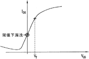
図1は、装置の種々のパラメータを、係数 k で拡縮するおおまかな傾向と相関を示したものである。一例として、旧来のトランジスタ構造体では、接合深さはチャネル長未満である必要がある。すると、図1に示したトランジスタ 100 では、チャネル長 102 の適切な長さが1000Åであることを考慮すると、接合深さ 101 は数百オングストロームの桁になるべきである。そうした浅い接合は、旧来の注入・拡散法ではつくることが難しい。また、チャネルへと超高濃度のドーピングを行うと、短チャネル効果をどうしても抑制してしまうことになる。こうした短チャネル効果には、ドレイン誘起障壁低下、閾値電圧のroll off(ロールオフ)、および閾値下伝達などがある。このような超高濃度ドープを行うと、漏洩が増してキャリア移動度が減少してしまう。閾値電圧が低いので、充分な増速駆動(overdrive)と妥当なスイッチング速度は実現できる。しかし図2に示したように、閾値が小さいと、閾値下漏洩電流がかなり大きくなってしまう。ゆえに、短かめのチャネルから得ようとしていた性能向上が、高濃度ドープに因るキャリア移動度の低さと漏洩の大きさに打ち消されてしまうのである。
FIG. 1 shows the general tendency and correlation of various parameters of the apparatus with a factor k. As an example, in a conventional transistor structure, the junction depth needs to be less than the channel length. Then, in the
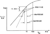
図3には、旧来の平面型CMOSトランジスタについての理想的な60mV/decadeの閾値下勾配と、短チャネル効果を受けた旧来の平面型CMOSトランジスタ構造体についての120mV/decadeから80mV/decadeの桁の閾値下勾配との、比較を描いてある。この図を見れば、旧来のナノスケール平面型CMOSトランジスタ技法において、閾値下漏洩電流を制御して減らすということがいかに難しいかがわかる。この問題は、ナノスケールCMOS回路に使われている低電力供給電圧によってさらに亢進してしまう──そうした低電力供給電圧は今や2.5Vの桁に乗っており、いずれはさらに低く、1.2Vの範囲にまで向かっていくことになる。良好なIon/Ioff比を得るには、トランジスタをオンにした際に、閾値下漏洩電流が、トランジスタ電流量の八倍以上(8 decades)低くなるべきである。そうではあるのだが、旧来の平面型装置で大電流と低閾値下漏洩の双方を実現するために必要な電圧振幅が、1.2V電源では充分には得られないのである。トランジスタをオンにするには、閾値電圧 VT を超えるような充分な電圧の増速駆動(overdrive)が要る。そしてトランジスタの閾値下漏洩を切るには、閾値電圧勾配の数倍(図3に約100mV/decadeとして示した)もが必要になるのである。 Figure 3 shows the ideal sub-threshold slope of 60mV / decade for a conventional planar CMOS transistor and 120mV / decade to 80mV / decade digits for a conventional planar CMOS transistor structure subjected to short channel effects. A comparison with the subthreshold slope is depicted. This figure shows how difficult it is to control and reduce the subthreshold leakage current in traditional nanoscale planar CMOS transistor technology. This problem is further exacerbated by the low power supply voltages used in nanoscale CMOS circuits--these low power supply voltages are now on the order of 2.5V, eventually lower, in the 1.2V range. It will go to. To obtain a good Ion / Ioff ratio, when the transistor is turned on, the subthreshold leakage current should be at least eight times lower than the amount of transistor current (8 decades). That being said, the voltage amplitude needed to achieve both high current and low threshold leakage in traditional planar devices is not sufficient with a 1.2V supply. To turn on the transistor, an overdrive with a sufficient voltage exceeding the threshold voltage VT is required. Then, several times the threshold voltage gradient (shown as about 100 mV / decade in FIG. 3) is required to cut off the sub-threshold leakage of the transistor.
こうした問題を狙って提案されたいくつかの設計では、超薄型基板(ultra-thin bodies)を持つトランジスタか、もしくは、トランジスタの他の寸法が縮小したのと同様にして表面空間電荷領域の寸法もとったようなトランジスタか、を用いている。また、デュアルゲート式もしくはダブルゲート式のトランジスタ構造体も、トランジスタの縮小のために提案されたものである。当該産業では通常、「デュアル(dual)ゲート」とは、別々の独立した電圧で駆動可能な前面ゲートと背面ゲートを具えたトランジスタのことを指す。そして「ダブル(double)ゲート」とは、両方のゲートが同じ電位で駆動されるような構造体のことを指す。ゲート基板を接続したトランジスタでは、動的な変動する閾値電圧が得られるので、トランジスタがオンのときには閾値が低く、トランジスタがオフのときには閾値が低くなるようにできる。ダブルゲート装置構造体の例としてはFinFETがある。「Triゲート」構造体およびサラウンディング(surrounding)ゲート構造体も提案されている。「Triゲート」構造体では、ゲートが、チャネルの三方の側に存在する。サラウンディングゲート構造体では、ゲートが、トランジスタチャネルをとりかこんでいる(囲繞している)。サラウンディングゲート構造体では、トランジスタチャネル全体に亙って望ましい制御ができるが、そうした構造体を実際につくるのはこれまでは難しかった。 Some designs proposed to address these issues include transistors with ultra-thin bodies or surface space charge region dimensions in the same way as other transistor dimensions have been reduced. It uses the transistor as it was. A dual-gate or double-gate transistor structure has also been proposed to reduce the size of the transistor. Typically in the industry, a “dual gate” refers to a transistor with a front gate and a back gate that can be driven by separate and independent voltages. “Double gate” refers to a structure in which both gates are driven at the same potential. In a transistor to which a gate substrate is connected, a dynamically varying threshold voltage can be obtained, so that the threshold value is low when the transistor is on and the threshold value is low when the transistor is off. An example of a double gate device structure is FinFET. "Tri-gate" structures and surrounding gate structures have also been proposed. In the “Tri Gate” structure, the gate is on three sides of the channel. In the surrounding gate structure, the gate surrounds (surrounds) the transistor channel. Surrounding gate structures provide desirable control over the entire transistor channel, but it has been difficult to actually make such structures.
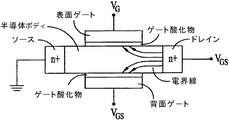
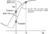
図4には、ドレインと、ソースと、ゲート絶縁体で半導体基板から隔てられた前面ゲートおよび背面ゲートとを具えた、デュアルゲート式MOSFETを示してある。さらに図3には、ドレインから発生する電界も示してある。デュアルゲート式MOSFETおよび/もしくはダブルゲート式MOSFETの持つ特性群は、旧来のバルク珪素MOSFETよりは優れたものである。これは、単一ゲートに較べれば、二つのゲートが、ドレイン電極のチャネルのソース側端から発生する電界を能く遮蔽するからである。サラウンディングゲートは、ドレイン電極のソース側から発生する電界をもっと能く遮蔽できる。図5には、デュアルゲート式MOSFET、ダブルゲート式MOSFET、もしくはサラウンディングゲート式MOSFETの向上した閾値下特性を、旧来のバルク珪素MOSFETの閾値下特性と比較するかたちでおおまかに示してある。デュアルゲート式および/もしくはダブルゲート式のMOSFETがオフになる際には、閾値下電流はより高速に減少する。 FIG. 4 shows a dual gate MOSFET having a drain, a source, and a front gate and a back gate separated from the semiconductor substrate by a gate insulator. Further, FIG. 3 also shows an electric field generated from the drain. The characteristics of dual-gate and / or double-gate MOSFETs are superior to conventional bulk silicon MOSFETs. This is because, compared to a single gate, the two gates effectively shield the electric field generated from the source side end of the channel of the drain electrode. The surrounding gate can more effectively shield the electric field generated from the source side of the drain electrode. FIG. 5 roughly shows the improved sub-threshold characteristics of a dual gate MOSFET, double gate MOSFET, or surrounding gate MOSFET compared to the sub-threshold characteristics of a conventional bulk silicon MOSFET. When the dual-gate and / or double-gate MOSFET is turned off, the subthreshold current decreases faster.
リソグラフィ基準寸法以下のチャネル寸法を持つMOSFET(FinFETなど)では、閾値下勾配が60mV/decadeになるようにでき、これは大型且つ旧来の平面型MOSFETに関連する閾値下勾配よりも小さい。しかしながら、閾値下漏洩をさらに減らせるような新規な装置構造体の需要が依然存在している。 For MOSFETs with channel dimensions below the lithography reference dimension (such as FinFET), the subthreshold slope can be 60 mV / decade, which is less than the subthreshold slope associated with large and traditional planar MOSFETs. However, there remains a need for new device structures that can further reduce subthreshold leakage.
トンネリング・トランジスタの閾値下勾配は、ゼロ近傍にできる。本明細書では、フォトリソグラフィー基準寸法(photolithographic dimension)未満の巾を持つトランジスタボディを囲うゲートを具えた、垂直トンネリング・トランジスタを開示する。こうしたサラウンディングゲートを具えた薄型トンネリング・トランジスタを使って、CMOS回路での閾値下漏洩を少なくできる。種々の実施形態群では、基板上に形成した非晶質構造体から結晶質ナノFinを成長させるか、結晶質基板をエッチングして結晶質基板から結晶質ナノFinを劃定するようにするか、あるいは、基板上に形成した非晶質構造体から結晶質ナノワイヤを成長させるか、のいずれかの手法により、リソグラフィ基準寸法以下の基板を得る。種々の実施形態群では、側壁スペーサー法を使って、リソグラフィ基準寸法以下を実現する。 The subthreshold slope of the tunneling transistor can be near zero. Disclosed herein is a vertical tunneling transistor with a gate surrounding a transistor body having a width less than the photolithographic dimension. By using a thin tunneling transistor with such a surrounding gate, subthreshold leakage in a CMOS circuit can be reduced. In various embodiments, whether to grow crystalline nanofin from an amorphous structure formed on the substrate, or to etch the crystalline substrate to determine crystalline nanofin from the crystalline substrate. Alternatively, a substrate having a lithography reference dimension or less is obtained by any method of growing crystalline nanowires from an amorphous structure formed on the substrate. In various embodiments, the sidewall spacer method is used to achieve sub-lithographic dimensions.
種々の態様群はトランジスタに関する。トランジスタに関する種々の実施形態群には、第一の方向についてリソグラフィ基準寸法以下である断面巾を有し且つ第一の方向に直交する第二の方向について最小フィーチャ寸法(minimum feature size)に対応する断面巾を有するようなナノFinと、そのナノFinの周りに在るサラウンディングゲート絶縁体と、ナノFinの周りにそのサラウンディングゲート絶縁体を間に挟んで在るサラウンディングゲートと、が含まれる。ナノFinの底端に在る第一の導電型を有する第一のソース/ドレイン領域、および、ナノFinの頂端に在る第二の導電型を有する第二のソース/ドレイン領域によって、その第一のソース/ドレイン領域と第二のソース/ドレイン領域との間を垂直方向に走るチャネル領域が劃定されている。種々のトランジスタにかかる実施形態には、基板表面上に形成され且つ少なくとも一方向についてリソグラフィ基準寸法以下である断面寸法を有するような結晶質柱と、その結晶質柱の周りに在るサラウンディングゲート絶縁体と、結晶質柱の周りにそのサラウンディングゲート絶縁体を間に挟んで在るサラウンディングゲートと、が含まれる。この結晶質柱を用いることで、第一の導電型を有する第一のソース/ドレイン領域と、第二の導電型を有する第二のソース/ドレイン領域との間を、垂直方向に走るチャネル領域が得られる。 Various embodiments relate to transistors. Various embodiments of the transistor include a cross-sectional width that is less than or equal to the lithography reference dimension in the first direction and corresponds to a minimum feature size in a second direction orthogonal to the first direction. Includes a nano-fin having a cross-sectional width, a surrounding gate insulator around the nano-fin, and a surrounding gate sandwiching the surrounding gate insulator around the nano-fin It is. The first source / drain region having the first conductivity type at the bottom end of the nano-Fin and the second source / drain region having the second conductivity type at the top end of the nano-Fin have its first A channel region is defined that runs vertically between one source / drain region and a second source / drain region. Embodiments of various transistors include a crystalline pillar formed on a substrate surface and having a cross-sectional dimension that is less than or equal to a lithography reference dimension in at least one direction, and a surrounding gate surrounding the crystalline pillar. An insulator, and a surrounding gate sandwiched around the crystalline pillar with the surrounding gate insulator interposed therebetween. By using this crystalline column, a channel region that runs vertically between the first source / drain region having the first conductivity type and the second source / drain region having the second conductivity type. Is obtained.
種々の態様群は、トランジスタの形成方法に関する。この方法の種々の実施形態群では、第一の方向についてリソグラフィ基準寸法以下である断面巾を有し、且つ第一の方向に直交する第二の方向について最小フィーチャ寸法に対応する断面巾を有するようなナノFinを形成する。また、サラウンディングゲート絶縁体をそのナノFinの周りにつくり、そしてサラウンディングゲートをナノFinの周りにそのサラウンディングゲート絶縁体を間に挟むようにして形成する。このナノFinを用いることで、第一の導電型を有する第一のソース/ドレイン領域と、第二の導電型を有する第二のソース/ドレイン領域との間を、垂直方向に走るチャネル領域が得られる。種々の実施形態群では、非晶質半導体柱を基板上に形成してから再結晶することで、ナノFinを形成する。種々の実施形態群では、結晶質基板に複数の溝をエッチングすることで、その基板からナノFinを形成する。 Various aspects relate to a method for forming a transistor. Various embodiments of the method have a cross-sectional width that is less than or equal to the lithography reference dimension for a first direction and a cross-sectional width that corresponds to a minimum feature dimension for a second direction orthogonal to the first direction. Form nano fins like this. In addition, a surrounding gate insulator is formed around the nano fin, and a surrounding gate is formed around the nano fin with the surrounding gate insulator interposed therebetween. By using this nano-fin, a channel region that runs vertically between the first source / drain region having the first conductivity type and the second source / drain region having the second conductivity type can be obtained. can get. In various embodiments, nanofins are formed by forming an amorphous semiconductor pillar on a substrate and then recrystallizing. In various embodiments, nanofins are formed from a crystalline substrate by etching a plurality of grooves.
本方法にかかる種々の実施形態群では、少なくとも一方向についてリソグラフィ基準寸法以下である断面寸法を有するような結晶質柱を形成する。この形成には、非晶質半導体柱を基板につくってから再結晶することでそうした結晶質柱を形成すること、が含まれる。サラウンディングゲート絶縁体をその結晶質柱の周りに形成してから、サラウンディングゲートを結晶質柱の周りにそのサラウンディングゲート絶縁体を間に挟むようにして形成する。こういった結晶質柱を用いることで、第一の導電型を有する第一のソース/ドレイン領域と、第二の導電型を有する第二のソース/ドレイン領域との間を、垂直方向に走るチャネル領域が得られる。 In various embodiments of the method, crystalline columns are formed having a cross-sectional dimension that is less than or equal to a lithography reference dimension in at least one direction. This formation includes forming an amorphous semiconductor pillar on the substrate and then recrystallizing it to form such a crystalline pillar. A surrounding gate insulator is formed around the crystalline column and then a surrounding gate is formed around the crystalline column with the surrounding gate insulator sandwiched therebetween. By using such a crystalline column, it runs vertically between the first source / drain region having the first conductivity type and the second source / drain region having the second conductivity type. A channel region is obtained.
これらその他の態様、実施形態、効果、および特徴は、本主題についての以降の記載および参照図面から明らかとなってくるであろう。 These other aspects, embodiments, effects, and features will become apparent from the following description of the subject matter and the referenced drawings.
以降の詳細な記載では、本主題を実施可能な特定の態様群および実施形態群を一例として示してある付随図面を参照している。これらの実施形態群は、当業者が本主題を実施できる程度に充分に詳細に記載してある。本主題の種々の実施形態同士が排他的である必然性はなく、或る実施形態の態様を別の実施形態の態様と組み合わせてもかまわない。他の実施形態を利用してもよく、また、構造的・論理的・電気的な変更を本主題の範囲から逸脱することなく加えることも可能である。以降の記載では、「ウェハ」("wafer")という語と「基板」("substrate")という語は同義であって、集積回路を作成可能な任意の構造体を一般に指し、集積回路製造中の種々の段階でのそうした構造体のことも指す。どちらの語にも、ドープ半導体および非ドープ半導体、支持半導体上もしくは絶縁材料上の半導体のエピタキシャル層、が含まれ、ひいては当該技術分野にて公知である他の構造体も包摂されている。「水平方向の」("horizontal")という語は本出願では、ウェハまたは基板の在来型の平面もしくは表面に対して平行な平面のことであると定義され、そのウェハもしくは基板の向きには依らない。「垂直方向の」("vertical")という語は、上記で定めた「水平方向」に直交する方向のことを指す。"on"(「上の」、「に付いた」)、"side"(「横の」)、"higher"(「高い」)、"lower"(「低い」)、"over"(「上の」、「被った」)、および"under"(「下の」、「下方の」)といった前置詞は、ウェハまたは基板の上面に位置する在来型の平面もしくは表面に対して定義されるものであって、そのウェハもしくは基板の向きには依らない。ゆえに以降の詳細な記載は、限定的な意味にとるべきものではない。そして本発明の範囲は、付随する請求項とその請求項が体現する均等な特徴の全範囲によってのみ定められる。 In the following detailed description, reference is made to the accompanying drawings, which show by way of illustration specific groups of embodiments and embodiments in which the present subject matter may be practiced. These embodiments are described in sufficient detail to enable those skilled in the art to practice the present subject matter. The various embodiments of the present subject matter are not necessarily mutually exclusive, and aspects of one embodiment may be combined with aspects of another embodiment. Other embodiments may be utilized and structural, logical, and electrical changes may be made without departing from the scope of the present subject matter. In the following description, the terms “wafer” and “substrate” are synonymous and generally refer to any structure capable of creating an integrated circuit, during integrated circuit manufacturing. It also refers to such a structure at various stages. Both terms include doped and undoped semiconductors, epitaxial layers of semiconductors on support semiconductors or insulating materials, and thus encompass other structures known in the art. The term “horizontal” is defined in this application as a plane parallel to the conventional plane or surface of a wafer or substrate, and the orientation of the wafer or substrate is It does not depend. The term “vertical” refers to a direction orthogonal to the “horizontal direction” defined above. "on" ("up", "attached to"), "side" ("horizontal"), "higher" ("high"), "lower" ("low"), "over" ("up" Prepositions such as "", "covered"), and "under" are defined relative to a conventional plane or surface located on the top surface of the wafer or substrate. However, it does not depend on the orientation of the wafer or substrate. The following detailed description is therefore not to be taken in a limiting sense. And the scope of the present invention is defined only by the appended claims and the full scope of equivalent features that they embody.
本主題は、サラウンディングゲートおよびリソグラフィ基準寸法以下であるチャネルを具えた、トンネリング・トランジスタに関する。トンネリング・トランジスタ構造体およびそれらの形成方法にかかる種々の実施形態群を、以下に述べてゆく。このような構造体としては、成長型ナノワイヤトンネリング・トランジスタ、成長型ナノFinトンネリング・トランジスタ、エッチング型ナノFinトランジスタ、がある。また以下では、ナノFinアレイのレイアウト、CMOS論理回路の例、ならびに高レベルの装置およびシステムについても述べる。 The present subject matter relates to a tunneling transistor with a surrounding gate and a channel that is less than or equal to a lithography reference dimension. Various embodiments related to tunneling transistor structures and methods of forming them are described below. Examples of such structures include a growth type nanowire tunneling transistor, a growth type nanofin tunneling transistor, and an etching type nanofin transistor. The following also describes the layout of the nanofin array, examples of CMOS logic circuits, and high-level devices and systems.
〔トンネリング・トランジスタ〕
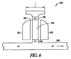
図6にはトランジスタ構造体603 を描いてある。トランジスタ構造体 603 は、垂直式であり且つリソグラフィ基準寸法以下であるようなチャネル 604 と、サラウンディングゲート 605 と、同じ導電型であるソース/ドレイン領域 606 およびソース/ドレイン領域 607 と、を具えている。こうしたトランジスタとしては、U.S. Application Nos. 11/397,430(2006年04月04日出願)および11/397,358(2006年04月04日出願)に記載されたものなどのナノFinトランジスタを用いてもよい。あるいはこうしたトランジスタとして、U.S. Application No. 11/397,527(2006年04月04日出願)に記載されたものなどのナノワイヤ・トランジスタを用いてもかまわない。サラウンディングゲート 605 は、基板もしくはチャネル 604 の周りにサラウンディングゲート絶縁体 608 を間に挟むようにして在る。この基板にドープを施すことで、底部のソース/ドレイン領域 606 と導電的に接続する導電線 609 を基板につくることができる。
[Tunneling transistor]
In FIG. 6, a transistor structure 603 is depicted. The transistor structure 603 comprises a
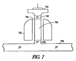
図7には、本主題の種々実施形態群にかかる、垂直式であり且つリソグラフィ基準寸法以下であるようなチャネルと、サラウンディングゲートと、異なる導電型である複数のソース/ドレイン領域と、を具えたトランジスタ構造体を描いてある。示した実施形態は、珪素基板内もしくはN+ウェル内に形成してある。別の実施形態では、他の導電型ドープを基板に施してもかまわない。 FIG. 7 illustrates a channel that is vertical and below the lithographic reference dimension, a surrounding gate, and a plurality of source / drain regions of different conductivity types, according to various embodiments of the present subject matter. The provided transistor structure is depicted. The illustrated embodiment is formed in a silicon substrate or N + well. In other embodiments, other conductivity type dopes may be applied to the substrate.
図6に示したトランジスタのように旧来は基板にN+ソース領域を形成していたが、そう
する代わりに、本主題の第一のソース/ドレイン領域 706 には、P+ドープを施す。さらには、その第一のソース/ドレイン領域 706 を回路内の他の素子に接続するソース配線 709 にも、P+ドープが施される。
Traditionally, N + source regions have been formed in the substrate as in the transistor shown in FIG. 6, but instead the first source / drain region 706 of the present subject matter is P + doped. Further, P + doping is also applied to the
少なめにドープされた薄型p型基板 704 が、第一のソース/ドレイン領域 706 の上に形成される。或る実施形態では、この形成を行うに際して0.1ミクロン技法を用い、それによってトランジスタの高さが約100nm、厚さが25nmから50nmの範囲になるようにする。別の実施形態群では、他の高さおよび/もしくは他の厚さ範囲を用いてもかまわない。
A lightly doped thin p-
N+ドープをされた第二のソース/ドレイン領域 707 を、珪素基板 704 の頂部に形成する。第二のソース/ドレイン領域 707 に接点 710 を形成することにより、トランジスタの第二のソース/ドレイン領域が、電子回路の他の素子に接続できるようになっている。この接続をする部位は、金属であってもよいし何か他の材料であってもよい。
An N + doped second source /
ゲート絶縁体層 708 を、薄型基板 709 の周りに形成する。この絶縁体としては、酸化物を用いてもよいし何か他の種類の誘電材料を用いてもかまわない。いくつかの実施形態群では、半導体基板の酸化によってこうした絶縁体をつくる。例えば或る実施形態では、珪素柱を熱酸化する工程によって、その柱の周りに酸化珪素のゲート絶縁体を設ける。
A gate insulator layer 708 is formed around the
制御ゲート 705 は、絶縁体層 708 の周りに形成する。当該技術分野で周知のように、制御ゲートに適切なバイアスをかけることで、第一のソース/ドレイン領域 706 と第二のソース/ドレイン領域との間のチャネル領域内にNチャネルを形成できる。
A
P+型である第一のソース/ドレイン領域を実施することも可能である。P+をドープする量は、N+よりもつねに少なくなるので、柱の頂部にはマスクをかける必要はなく、柱はN+のままになるであろう。得られる柱の側壁下にはP+領域が在り、頂部にはP+領域が在る。柱は薄いので、P+領域は柱の下で拡散し融合することになる。或る実施形態では、トランジスタ構造体が、成長式もしくは堆積式のゲート絶縁体と、側壁エッチング法でつくられたサラウンディングゲートと、を有する。 It is also possible to implement a first source / drain region that is P + type. Since the amount of P + doping is always less than N + , there is no need to mask the top of the pillar, and the pillar will remain N + . The lower wall of the resulting column has P + region, the top there is a P + region. Since the pillar is thin, the P + region will diffuse and merge under the pillar. In some embodiments, the transistor structure includes a growth or deposition gate insulator and a surrounding gate made by sidewall etching.
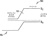
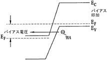
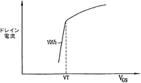
図8および図9には、図6のトランジスタの挙動についてのエネルギー帯(エネルギーバンド)図を描いてある。各図の上側の線は伝導帯のエネルギーを、下側の線は価電子帯のエネルギーを、それぞれ示している。図8は、本主題の種々の実施形態群にかかる、トランジスタゲートにバイアスをかけていないときの図7のトンネリング・トランジスタの電気的な挙動を、エネルギー帯図で示したものである。この図には、チャネルおよびN+である第二のソース/ドレイン領域811 、ならびにP+である第一のソース/ドレイン領域 812 が示されている。非導電性条件では、ソース/ドレイン領域間に大きな障壁 813 が存在する。図9は、本主題の種々の実施形態群にかかる、トランジスタゲートにバイアスをかけるときの図7のトンネリング・トランジスタの電気的な挙動を、エネルギー帯図で示したものである。トランジスタの電気的な挙動は、MOSでゲートされたpinダイオードに基づいたものである。ゲートにバイアスをかけることで、電子濃度がいったん減少すると、電子チャネルの形成が誘導されるような導電条件をつくりだせる。トンネル接合 914 を、このチャネルのP+側に形成する。ドレインにバイアスをかけることで、帯を曲げて、N型領域導電帯がソース領域の価電子帯のきわよりも下にくるようにできる。すると電子が、ソース価電子帯から、誘導されたn型チャネル領域へとトンネル移動し、そうしてドレイン電流が得られることになる。チャネルの導電帯のきわが、ソースの価電子帯の下へと引き下げられるまでは、トンネリングは起こりえない。このため、turn-on特性は非常に鋭く、図10に示すように、閾値下勾配が、トンネリング・トランジスタとしての理想値すなわち0mV/decadeに近づくことになる。
FIGS. 8 and 9 are energy band diagrams for the behavior of the transistor of FIG. The upper line in each figure shows the energy of the conduction band, and the lower line shows the energy of the valence band. FIG. 8 is an energy band diagram illustrating the electrical behavior of the tunneling transistor of FIG. 7 when the transistor gate is not biased, according to various embodiments of the present subject matter. This figure shows a channel and a second source /
図10は、本主題の種々の実施形態群にかかる、図7のトンネリング・トランジスタについてのドレイン電流vs.トンネリング・トランジスタゲート-ソース電圧をプロットしたものであり、閾値下漏洩電流を示してある。このプロットでは、閾値下電流1015 が非常にきつい勾配 "S" を示しており、これはトンネリング・トランジスタの実施形態群でのバイアスかけに起因するものである。図10の縦軸のドレイン電流はlog scaleであり、横軸のVGSはlinearである。 FIG. 10 is a plot of drain current vs. tunneling transistor gate-source voltage for the tunneling transistor of FIG. 7 according to various embodiments of the present subject matter, illustrating subthreshold leakage current. In this plot, the subthreshold current 1015 shows a very tight slope “S” due to biasing in the tunneling transistor embodiments. The drain current on the vertical axis in FIG. 10 is log scale, and VGS on the horizontal axis is linear.
〔垂直式であり且つリソグラフィ基準寸法以下であるチャネルを形成する方法〕
以下の記述では、珪素トランジスタの実施形態群を参照する。当業者は、本開示を通読し把握した上で、本明細書に教示したところをどのように用いれば、リソグラフィ基準寸法以下であるチャネルを具えたトンネリング・トランジスタを他の半導体を使って形成できるかについてを理解できるであろう。
[Method of forming a channel that is vertical and is equal to or smaller than the lithography reference dimension]
In the following description, reference is made to embodiments of silicon transistors. Those skilled in the art, after reading and understanding the present disclosure, can use other semiconductors to form tunneling transistors with channels that are less than or equal to the lithography reference dimensions, using the teachings herein. You will understand that.
〔ナノワイヤ基板の成長方法〕
図11Aから図11Hには、本主題の種々の実施形態群にかかる、トンネリング・トランジスタのための垂直式チャネルを得るための、ナノワイヤ基板の成長工程を描いてある。示した工程では、サラウンディングゲートを具えた結晶質ナノロッドを形成する。示した工程については、 "Nanowire Transistor With Surrounding Gate" U.S. Application No. 11/397,527(2006年04月04日出願、この参照により本開示に含まれる)に記載されている。
[Growth method of nanowire substrate]
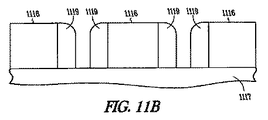
11A-11H depict a nanowire substrate growth process to obtain a vertical channel for a tunneling transistor according to various embodiments of the present subject matter. In the process shown, crystalline nanorods with surrounding gates are formed. The steps shown are described in “Nanowire Transistor With Surrounding Gate” US Application No. 11 / 397,527 (filed Apr. 4, 2006, incorporated herein by reference).
図11Aには、基板 1117 上の第一の層 1116 を示してある。第一の層 1116 には複数の孔 1118 がつくられている。この層に孔を劃定するにあたっては、第一の層をエッチングすることで行える。種々の実施形態群では、複数の孔 1118 を珪素基板 1117 上の窒化珪素層 1116 に穿つときに、それらの孔が窒化珪素層を貫通して珪素基板に届くようにする。示した実施形態では、それらの孔の寸法が、最小フィーチャ寸法に対応するようにつくる。各孔の中心は、ナノワイヤ・トランジスタの所望の位置に対応する。ナノワイヤ・トランジスタのアレイの、行と列についての中心間間隔を、2Fに設定できる。
FIG. 11A shows the
孔を第一の層にエッチングして穿った後に、酸化物の層をその第一の層の上に設ける。種々の実施形態群では、窒化珪素層の上に酸化珪素を形成する。いくつかの実施形態群では、化学気相蒸着(CVD)工程により酸化珪素の堆積を行う。 After the holes have been etched into the first layer, an oxide layer is provided over the first layer. In various embodiments, silicon oxide is formed on the silicon nitride layer. In some embodiments, silicon oxide is deposited by a chemical vapor deposition (CVD) process.
図11Bには、酸化物を異方性エッチングして、孔の側部に付いた酸化物側壁 1119 を残すようにしたその後の、構造体を示してある。この酸化物側壁 1119 には、得られる孔の寸法を縮めるという効果がある。得られた構造体を平坦化する。100nm技法では例えば、酸化物側壁によって、孔の寸法を約30nmまで縮める。この例では、トランジスタの基板領域の厚さが、フィーチャ寸法の三分の一の値のorderになると考えられる。いくつかの実施形態群では、化学的・機械的研磨(CMP)工程を使って構造体を平坦化する。
FIG. 11B shows the structure after the oxide has been anisotropically etched to leave
図11Cには、得られた構造体の上に、非晶質半導体材料 1120 の厚い層を被せたさまを示してある。この非晶質材料が、側壁 1119 で劃定した孔を埋めている。種々の実施形態群では、非晶質材料として非晶質珪素を用いて堆積する。図11Dには、得られる構造体を(CMPなどで)平坦化したその後に、孔の中だけに非晶質半導体材料が残るようすを描いている。
FIG. 11C shows the resulting structure overlaid with a thick layer of
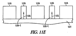
図11Eには、側壁(酸化珪素でできた側壁など)を除去した後に得られる構造体を示してある。この構造体を加熱処理し、固相エピタキシー(SPE)などの公知の手法を使って、非晶質半導体 1120 (非晶質珪素など)を結晶化して結晶質ナノロッド( 1120-C を振って示した)をつくる。非晶質半導体柱 1120 は、半導体ウェハ(珪素ウェハなど)と
接続しており、したがって非晶質半導体柱 1120 の結晶成長は、そのウェハ中の結晶を種としたものとなる。SPE工程による結晶形成を、図11Eに矢印 1121 で示した。
FIG. 11E shows the structure obtained after removing the sidewall (such as a sidewall made of silicon oxide). This structure is heat treated, and amorphous semiconductor 1120 (such as amorphous silicon) is crystallized using a known method such as solid phase epitaxy (SPE) to show crystalline nanorods (1120-C). A). The
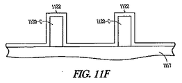
図11Fには、第一の層(窒化珪素など)を除去した後の構造体を描いており、ここでは結晶質ナノロッド 1120-C が基板表面からのびあがるようにして残っている。そしてその後にゲート絶縁体 1122 を得られる構造体に被せている。或る実施形態では、ゲート絶縁体の形成に熱酸化工程を使う。つまり、ウェハが珪素ウェハであって且つナノロッドが結晶質珪素ナノロッドであるような実施形態の場合には、ゲート絶縁体は酸化珪素となる。High K絶縁体などの他のゲート絶縁体を使ってもかまわない。
FIG. 11F depicts the structure after removal of the first layer (such as silicon nitride), where the crystalline nanorods 1120-C remain so as to lift from the substrate surface. After that, a
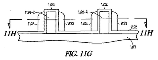
ゲート材料 1123 を結晶質ナノロッド 1120-C の側壁に付けてつくった後の構造体について、図11Gに側面図を、図11Hに図11Gの線11H-11H で切った断面図を、それぞれ示した。或る実施形態では、ゲート材料を堆積してから、得られる構造体をエッチングして、ナノロッドの側壁に付いた分だけしかゲート材料を残さないようにする。種々の実施形態群では、ポリシリコンをゲート材料として使う。柱の高さによってトランジスタのチャネル長が定まることになり、この柱の高さを最小リソグラフィ基準寸法(minimum lithographic dimensions)よりも小さくできる。種々の実施形態群では、チャネル長を約100nmのオーダー(order)にする。こうした巻きつき式(wraparound)ゲートを具えたナノロッドを用いて、surrounding式(巻きつき式)のゲートを具えたナノワイヤ・トランジスタを作成できる。単体のトランジスタもしくはトランジスタアレイを形成するには、 "Nanowire Transistor With Surrounding Gate" U.S. Application No. 11/397,527(2006年04月04日出願)に記載の手法に従えばよい。
FIG. 11G shows a side view and FIG. 11H shows a cross-sectional view taken along
〔ナノFin基板の成長方法〕
図12Aから図12Lには、本主題の種々の実施形態群にかかる、トンネリング・トランジスタのための垂直式チャネルを得るための、ナノFin基板の成長工程を描いてある。示した工程については、 "Grown Nanofin Transistors" U.S. Application No. 11/397,430(2006年04月04日出願、この参照により本開示に含まれる)に記載されている。
[Growth method of nano fin substrate]
12A-12L depict a nano-Fin substrate growth process to obtain a vertical channel for a tunneling transistor according to various embodiments of the present subject matter. The steps shown are described in “Grown Nanofin Transistors” US Application No. 11 / 397,430 (filed Apr. 4, 2006, incorporated herein by reference).
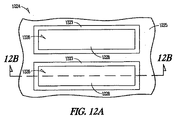
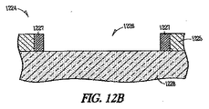
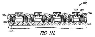
ここにて開示するのは、ナノFinトランジスタ、および、垂直方向の非晶質珪素ナノFinを基板上で再結晶させて単結晶珪素ナノFinトランジスタを作成するような構築法、である。本主題の態様群では、垂直チャネルを具えたナノFinトランジスタを提供し、こうしたトランジスタは、Finの底部に在る第一のソース/ドレイン領域と、Finの頂部に在る第二のソース/ドレイン領域とを有する。 Disclosed here is a nano-Fin transistor and a construction method in which a single-crystal silicon nano-Fin transistor is produced by recrystallizing vertical amorphous silicon nano-Fin on a substrate. Embodiments of the present subject matter provide nano-Fin transistors with vertical channels, such transistors having a first source / drain region at the bottom of the Fin and a second source / drain at the top of the Fin. And having a region.
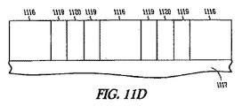
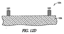
半導体構造体 1224 の上面図を図12Aに、線 12B-12B に沿った断面図を図12Bに、それぞれ示してある。半導体構造体 1224 は、窒化珪素層 1225 と、窒化珪素層 122 に在る孔 1226 と、孔の壁に沿った非晶質珪素でできた側壁スペーサー 1227 と、を有する。孔を、窒化珪素層にエッチングして穿ってから、非晶質珪素を堆積させて異方性エッチングして側壁に付いたところだけに残す。孔 1226 をエッチングするときには、窒化珪素層 1225 を貫通して、珪素ウェハもしくは基板 1228 に届くようにする。
A top view of the
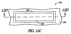
窒化珪素層を除去した後の構造体1224 の上面図を図12Cに、線 12D-12D に沿った断面図を図12Dに、それぞれ示してある。示しているように、窒化珪素層を除去した後に、側壁 1227 が、非晶質珪素の自立した細い領域として残ることになる。こうして得られる自立した珪素からなるパターンは、おおまかには細長い矩形なので、「競技路」("racetrack")パターンとも呼ばれている。線巾は、保護(マスキング)工程・リソグラフィ工程に依ってではなく、非晶質珪素の厚さに依って決まってくる。種々の実施形態群では例えば、非晶質珪素の厚さは、約20nmから50nmである。固相エピタキシャル(SPE)成長工程を使って、こうした非晶質珪素の自立した細い領域を再結晶させられる。SPE成長工
程には、アニーリング(加熱処理)が含まれ、これによって構造体中の非晶質珪素の結晶化を、珪素基板 1228 との界面から発動させる。この界面は結晶成長の種として機能し、珪素の自立した細い領域の残りの部分を這いのぼって結晶化が進行してゆくことになる。
A top view of
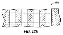
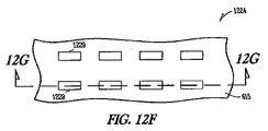
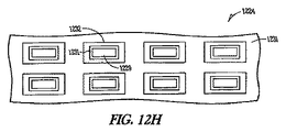
図12Eには、マスク層を塗布した後の構造体 1224 の上面図を描いてある。網かけしてあるところはエッチングされた部分であって、結晶質珪素からできた自立型Finが残っている。自立型Fin 1229 のなすパターンについて、図12Fに上面図を、図12Gに線 12G-12G に沿った断面図を、それぞれ示した。埋め込み式のドープ領域 1230 は、第一のソース/ドレイン領域として機能する。種々の実施形態群では、こうした埋め込み式のドープ領域をパターン化して、Finのアレイの行方向か列方向かに沿わせた導電線を作成可能である。
FIG. 12E depicts a top view of
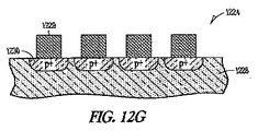
図12Hには構造体の上面図を示してあり、ここではFinがゲート絶縁体 1231 とゲート 1232 に囲まれている。このゲート絶縁体は、堆積してつくってもよいし、何らかの別の手法でつくってもかまわない。例えば酸化珪素を、珪素Finの上に熱酸化工程を用いて形成することもできる。ゲートとしては任意のゲート材料を使用でき、例えばポリシリコンもしくは金属を使用できる。ゲート材料を堆積して異方性エッチングすることで、ゲート材料を、ゲート絶縁体を具えたFin構造の側壁上にのみ残す。配線の向きは、「x方向」か「y方向」かのいずれかにできる。
FIG. 12H shows a top view of the structure, where Fin is surrounded by a
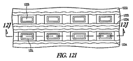
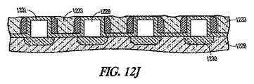
図12Hの構造体
を絶縁体 1233 で埋め戻し、ゲート配線 1234 を「x方向」(Finの長手側に沿った方向)につくった状態に関して、図12Iに上面図を、図12Jに線 12J-12J に沿った断面図を、それぞれ示した。種々の実施形態群では、構造体を酸化珪素で埋め戻す。埋め戻した絶縁体に、Finの側部に沿って走らせるようにして溝をつくる。そしてゲート線をその溝の中につくる。種々の実施形態群では、ひとつのゲート線がFinの一方の側に沿って走っており、Fin構造体のサラウンディングゲートと接続している。いくつかの実施形態群では、第一のゲート線をFinの第一の側に、第二のゲート線をFinの第二の側に、それぞれつくる。ゲート配線材料(ポリシリコンもしくは金属など)を堆積して異方性エッチングし、側壁上にのみ残すようにできる。ゲート配線材料は、Finのサラウンディングゲートと接続しているのが好ましい。種々の実施形態群では、ゲート材料およびゲート配線材料をエッチングして、ゲートおよびゲート配線がFinの頂部の下にくるように凹ませる。構造体の全体を絶縁体(酸化珪素など)で埋め戻してから、平坦化して表面に酸化物だけが残るようにできる。こうした柱もしくはFinの頂部は、エッチングを使って露出させられる。旧来の技法を用いて、第二のソース/ドレイン領域を、Finの頂部に注入してつくり、また、ドレイン領域への金属接点を作成できる。例えば、金属配線を「x方向」に走らせ、埋め込み式ソース配線を図の紙面に垂直な方向に走らせるようにできる。
The structure of FIG. 12H is backfilled with an
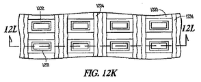
構造体を絶縁体で埋め戻して、ゲート配線を「y方向」(Finの短手側に沿った方向)につくった状態に関して、図12Kに上面図を、図12Lに線12L-12L に沿った断面図を、それぞれ示した。溝はFinの側部を「y方向に」沿って拓けている。ゲート配線材料 1234 (ポリシリコンもしくは金属など)を堆積して異方性エッチングし、側壁上にのみ残すようにしてFin上のゲートに接続させるようにできる。種々の実施形態群では、ゲート材料およびゲート配線材料をエッチングして、ゲートおよびゲート配線がFinの頂部の下にくるように凹ませる。構造体の全体を絶縁体 1233 (酸化珪素など)で埋め戻してから、平坦化して表面に埋め戻し絶縁体だけが残るようにできる。その後に、柱の頂部ならびに旧来の技法を用いてそこに注入されたドレイン領域1235およびドレイン領域への金属接点1236へと、接点開口部およびドレインドープ領域をエッチングしてつくることも可能である。例えば、金属配線を図の紙面に垂直な方向に走らせ、埋め込み式ソース配線 1230 を「x方向」に走らせるようにできる。非晶質珪素の堆積に先立って、埋め込み式ソース/ドレインをパターン化して注入する。図12Lには、仕上がったFin構造体のうちのひとつを提示しており、この構造体は、ドレイン/ソース領域と、凹んだゲートと、ソース/ドレイン領域配線と、を有している。こうしたナノFinFETでは、W/L比を大きくできるため、ナノワイヤFETに比して多量の電流を通すことが可能である。
FIG. 12K shows a top view and FIG. 12L shows a
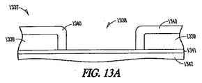
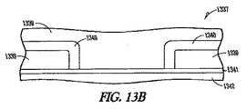
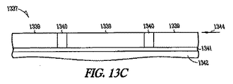
〔ナノFin基板のエッチング方法〕
ここにて開示するのは、ナノFinトランジスタ、ならびに、基板もしくはウェハをエッチングしてナノFinを得てそのナノFinを使い単結晶ナノFinトランジスタを作成するような構築法、である。以降の詳細な説明では、付随する図面を参照して、本主題を実施可能な特定の態様群および実施形態群をあくまで例示として示す。当業者には、本開示を読んで理解した上で、他の半導体を用いてナノFinを作成する手法がわかるであろう。本主題の態様群では、垂直チャネルを具えたナノFinトランジスタを提供し、こうしたトランジスタは、Finの底部に在る第一のソース/ドレイン領域と、Finの頂部に在る第二のソース/ドレイン領域とを有する。
[Nano Fin substrate etching method]
Disclosed here is a nano-Fin transistor and a construction method in which a nano-fin is obtained by etching a substrate or wafer and a single-crystal nano-Fin transistor is created using the nano-fin. In the following detailed description, reference is made to the accompanying drawings that show, by way of illustration, specific aspects and embodiments in which the present subject matter may be implemented. Those of ordinary skill in the art will understand how to make nanofins using other semiconductors upon reading and understanding the present disclosure. Embodiments of the present subject matter provide nano-Fin transistors with vertical channels, such transistors having a first source / drain region at the bottom of the Fin and a second source / drain at the top of the Fin. And having a region.
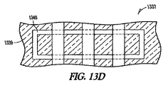
或る実施形態では、窒化珪素を珪素ウェハ上に堆積してから、この窒化珪素を非晶質珪素(a-silicon)の層で蔽う。図13Aには、孔1338 を非晶質珪素 1339 内に劃定して、側壁スペーサー 1340 を形成した後の、構造体 1337 の側面図を示してある。孔 1338 は窒化珪素層 1341 内に展延していて、窒化珪素層 1341 は基板 1342 (珪素ウェハなど)の上に位置している。種々の実施形態群では、非晶質珪素を酸化することで側壁スペーサーをつくる。図13Bには、非晶質珪素の厚い層 1339 で覆った後の、構造体 1337 の側面図を示してある。図13Cには、矢印 1344 に示したところで平坦化した後の構造体 1337 を示してある。こうした平坦化は、非晶質珪素の上部に載った酸化物を除去できる高さにまで、少なくとも行う。構造体の平坦化にあたっては、例えば化学的・機械的研磨(CMP)工程を使用できる。こうして、表面に露出した酸化物 1340 でできた細長い矩形のパターンか残る。このパターンのことを「競技路」("racetrack")パターンとも呼ぶ。このパターンの線巾は、保護(マスキング)工程・リソグラフィ工程に依ってではなく、酸化物の厚さに依って決まってくる。種々の実施形態群では例えば、酸化物の厚さは、約20nmから50nmである。
In some embodiments, silicon nitride is deposited on a silicon wafer and then the silicon nitride is covered with a layer of amorphous silicon (a-silicon). FIG. 13A shows a side view of
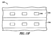
図13Dには、競技路パターンに被せたマスクを描いてあり、このマスクは酸化物の部分を選択的に蔽い、酸化物のその他の部分が露出するようにする。酸化物のこの露出した部分には斜線をかけてあり、ここが除去されることになる。エッチング工程(水酸化カリウム KOH エッチングなど)を施して、非晶質珪素を除去する。図13Dに示した、保護工程とエッチング工程の後に残る酸化物もしくは酸化物の一部が、エッチング工程中に窒化物を保護することになる。非晶質珪素を除去した後に窒化物 1341 をエッチングして、珪素異方性エッチングを使って、ウェハ 1342 を窒化物層下の所定の深さまでエッチングできる。窒化物パターンによって珪素の局部をエッチングから保護することで、珪素でできた珪素Fin 1343 を、珪素ウェハの今や低くなった表面から突き出したようなかたちで得ることができる(図13E参照)。Finの頂部とFinの底部に在る溝とにドーパントを注入した後の、構造体の上面図を図13Fに、側面図を図13Gに、それぞれ示した。図13Fに示したように、溝に注入したドーパントによって、導電線 1344 (ソース線など)ができている。また、Finの底もしくは底部に注入したドーパントによって、ソース/ドレイン領域ができている。Finは極薄なので、溝へのドープをするとFinの下部に完全に拡散させられる。こうした細片は行方向に並べてもよいし列方向に並べてもよい。
FIG. 13D depicts a mask over the track pattern that selectively covers the oxide portion and exposes other portions of the oxide. This exposed portion of oxide is shaded and will be removed. An amorphous silicon is removed by performing an etching process (potassium hydroxide KOH etching or the like). The oxide or part of oxide remaining after the protection and etching steps shown in FIG. 13D will protect the nitride during the etching step. After removing the amorphous silicon, the
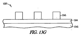
図13Hには、ゲート絶縁体1345 をFin 1343 の周りに形成して、ゲート材料 1346 をFin 1343 の周りにそのゲート絶縁体 1345 を間に挟んで形成した後の、構造体1337 を描いてある。或る実施形態では例えば、熱酸化工程を用いて珪素Finを酸化する。種々の実施形態群では、ゲート材料 1346 として、ポリシリコンもしくは金属を使用できる。
FIG. 13H depicts
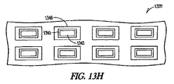
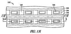
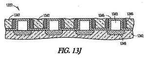
アレイの第一の実施形態に関して、図13Iに上面図を、図13Jに線 13J-13J に沿った断面図を、それぞれ示した。構造体 1337 を絶縁体 1347 (酸化物など)で埋め戻してから、溝をFinの脇につくる。ゲート配線材料 1348 (ポリシリコンもしくは金属など)を堆積して異方性エッチングし、側壁に付いたところだけに残して、Finのサラウンディングゲート1346 に接続するようにできる。ゲート材料およびゲート配線材料をエッチングして、Finの頂部の下にくるように凹ませることが可能である。構造体の全体を酸化物で埋め戻してから、平坦化して表面に酸化物だけが残るようにできる。その後に、柱の頂部ならびに旧来の技法を用いてそこに注入されたドレイン領域およびドレイン領域への金属接点へと、接点開口部およびドレインドープ領域をエッチングしてつくることも可能である。この場合、金属配線を「x方向」に走らせ、埋め込み式ソース配線 1349 を図の紙面に垂直な方向に走らせるようにできる。
Regarding the first embodiment of the array, FIG. 13I shows a top view and FIG. 13J shows a cross-sectional view along line 13J-13J. After the
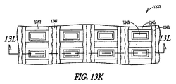
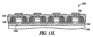
アレイの第二の実施形態に関して、図13Kに上面図を、図13Lに線 13L-13L に沿った断面図を、それぞれ示した。構造体 1337 は絶縁体 1347 (酸化物など)で埋め戻されており、溝がFin 1343 の脇の「y方向」に沿ってつくられている。ゲート配線材料 1348 (ポリシリコンもしくは金属など)を堆積して異方性エッチングし、側壁に付いたところだけに残して、Fin上のゲートに接続するようにできる。ゲート材料およびゲート配線材料をエッチングして、Finの頂部の下にくるように凹ませることが可能である。構造体の全体を絶縁体(酸化物など)で埋め戻してから、平坦化して表面に酸化物だけが残るようにできる。その後に、柱の頂部ならびに旧来の技法を用いてそこに注入されたドレイン領域およびドレイン領域への金属接点へと、接点開口部およびドレインドープ領域をエッチングしてつくることも可能である。この場合、金属配線を図の紙面に垂直な方向に走らせ、埋め込み式ソース配線を「x方向」に走らせるようにできる。
Regarding the second embodiment of the array, FIG. 13K shows a top view and FIG. 13L shows a cross-sectional view along
アレイの第一の実施形態でも第二の実施形態でも、サラウンディングゲート絶縁体およびサラウンディングゲートの形成に先立って、埋め込み式ソース/ドレインをパターン化して注入できる。図13Lには、仕上がったFin構造体のうちのひとつを提示しており、この構造体は、ドレイン/ソース領域 1350 およびドレイン/ソース領域1351 と、凹んだゲート 1346 と、ソース/ドレイン領域配線 1349 と、を有している。こうしたナノFinFETでは、W/L比を大きくできるため、ナノワイヤFETに比して多量の電流を通すことが可能である。
In both the first and second embodiments of the array, the buried source / drain can be patterned and implanted prior to forming the surrounding gate insulator and the surrounding gate. FIG. 13L presents one of the finished Fin structures, which includes a drain /
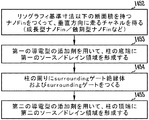
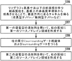
図11Aから図11H、図12Aから図12L、および図13Aから図13Lに示した工程は、フロー図を以っておおまかに表すこともでき、その例が図14と図15である。図14には、本主題の種々の実施形態群にかかる、トンネリング・ナノFinトランジスタを形成する方法を示してある。示した実施形態では、 1452 にて、ナノFinの断面積がリソグラフィ基準寸法以下となるようにして形成する。垂直方向に走るチャネルが、ナノFin内に劃定されることになる。このナノFinの形成にあたっては、図12Aから図12Lに示したようにして結晶質ナノFinを成長させることで行うことができるし、あるいは、図13Aから図13Lに示したようにして結晶質基板をエッチングしてナノFinを劃定することで行ってもよい。1453 では、第一のソース/ドレイン領域を柱の底端に作成する。この第一のソース/ドレイン領域は第一の導電型を有し、例えばP+領域を有する。第一のソース/ドレイン領域の形成は、ナノFinの形成に先立って行うことが可能である。また、ナノFinの形成後に第一のソース/ドレイン領域をつくることもできる。その理由は、ナノFinが非常に薄いので、注入されたドーパントがナノFinの下方に完全に拡散できるからである。 1454 では、サラウンディングゲート絶縁体をナノFinの周りにつくってから、サラウンディングゲートをナノFinの周りにそのサラウンディングゲート絶縁体を間に挟むようにしてつくる。 1455 では、第二のソース/ドレイン領域をナノFinの頂端に形成する。この第二のソース/ドレイン領域は、第一の導電型とは異なる第二の導電型(例えばN+)を有する。なお、第一のソース/ドレイン領域が第二の導電型(N+)を有し、第二のソース/ドレイン領域が第一の導電型(P+)を有してもよい、ということに留意されたい。 The steps shown in FIGS. 11A to 11H, FIGS. 12A to 12L, and FIGS. 13A to 13L can be roughly represented by flow diagrams, and examples thereof are FIGS. 14 and 15. FIG. 14 illustrates a method of forming a tunneling nano-Fin transistor according to various embodiments of the present subject matter. In the illustrated embodiment, at 1452, the nanofin cross-sectional area is formed to be less than or equal to the lithography reference dimension. A channel running in the vertical direction will be determined in the nanofin. The nano-fin can be formed by growing the crystalline nano-fin as shown in FIGS. 12A to 12L, or the crystalline substrate as shown in FIGS. 13A to 13L. Etching may be performed to determine nano-Fin. In 1453, a first source / drain region is created at the bottom end of the column. The first source / drain region has a first conductivity type, for example, a P + region. The formation of the first source / drain region can be performed prior to the formation of the nano fins. In addition, the first source / drain region can be formed after the nanofin is formed. The reason is that the nanofin is so thin that the implanted dopant can completely diffuse below the nanofin. In 1454, a surrounding gate insulator is made around the nanofin, and then a surrounding gate is made around the nanofin with the surrounding gate insulator in between. In 1455, a second source / drain region is formed at the top of the nanofin. The second source / drain region has a second conductivity type (for example, N + ) different from the first conductivity type. The first source / drain region may have the second conductivity type (N + ), and the second source / drain region may have the first conductivity type (P + ). Please keep in mind.
図15には、本主題の種々の実施形態群にかかる、トンネリング・トランジスタのためのリソグラフィ基準寸法以下のトランジスタボディの成長方法を示してある。 1556 では、基板上の非晶質半導体から、結晶質柱を、その断面積がリソグラフィ基準寸法以下となるようにして成長させる。垂直方向に走るチャネルが、結晶質柱内に劃定されることになる。この柱は、図11Aから図11Hに示したようなナノワイヤであってもよいし、あるいは、図12Aから図12Lに示したようなナノFinであってもかまわない。 1557 では、第一のソース/ドレイン領域を、柱の底端に作成する。この第一のソース/ドレイン領域は第一の導電型を有し、例えばP+領域を有する。第一のソース/ドレイン領域の形成は、結晶質柱の形成に先立って行うことが可能である。また、結晶質柱の形成後に第一のソース/ドレイン領域をつくることもできる。その理由は、柱が非常に薄いので、注入されたドーパントが柱の下方に完全に拡散できるからである。 1558 では、サラウンディングゲート絶縁体を柱の周りにつくってから、サラウンディングゲートを柱の周りにそのサラウンディングゲート絶縁体を間に挟むようにしてつくる。 1559 では、第二のソース/ドレイン領域を柱の頂端に形成する。この第二のソース/ドレイン領域は、第一の導電型とは異なる第二の導電型(例えばN+)を有する。なお、第一のソース/ドレイン領域が第二の導電型(N+)を有し、第二のソース/ドレイン領域が第一の導電型(P+)を有してもよい、ということに留意されたい。単体のトランジスタ又はトランジスタアレイが形成される。 FIG. 15 illustrates a method for growing a transistor body below a lithographic reference dimension for a tunneling transistor according to various embodiments of the present subject matter. In 1556, a crystalline column is grown from an amorphous semiconductor on a substrate so that its cross-sectional area is less than or equal to a lithography reference dimension. A channel running in the vertical direction will be defined in the crystalline column. The pillars may be nanowires as shown in FIGS. 11A to 11H, or nanofins as shown in FIGS. 12A to 12L. In 1557, a first source / drain region is created at the bottom end of the column. The first source / drain region has a first conductivity type, for example, a P + region. The formation of the first source / drain region can be performed prior to the formation of the crystalline column. In addition, the first source / drain region can be formed after the formation of the crystalline column. The reason is that the column is so thin that the implanted dopant can completely diffuse below the column. In 1558, a surrounding gate insulator is made around a pillar and then a surrounding gate is made around the pillar with the surrounding gate insulator in between. In 1559, a second source / drain region is formed at the top end of the column. The second source / drain region has a second conductivity type (for example, N + ) different from the first conductivity type. The first source / drain region may have the second conductivity type (N + ), and the second source / drain region may have the first conductivity type (P + ). Please keep in mind. A single transistor or transistor array is formed.
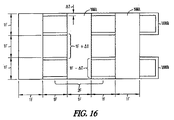
〔ナノFinアレイ〕
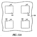
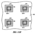
図16は、種々の実施形態群にかかる、トンネリング・ナノFinトランジスタのアレイのための、ナノFinの上面からみたレイアウトである。この図では、側壁スペーサー 1660
でできた二つの「競技路」を示しており、エッチングで側壁スペーサーの一部を取り除いたさまも描いてある。孔を使って、側壁スペーサー競技路が最小フィーチャ寸法(1F)となるようにつくってある。マスク片 1661 の巾は最小フィーチャ寸法(1F)であり、またマスク片 1661 同士の間隔も最小フィーチャ寸法(1F)になっている。示したレイアウトでは、ナノFinの列の中心間距離がほぼ2Fになっていて、またナノFinの行の中心間距離がほぼ1Fとなっている。また図16に示してあるように、ナノFinは、孔の壁に付いた側壁スペーサーからつくってあるので、第一の行と第二の行との中心間距離が、長さ1FからナノFinの厚みに応じた量だけ若干縮んだ長さ(1F-ΔT)となっている。そして、第二の行と第三の行との中心間距離が、長さ1FにナノFinの厚みに応じた量だけ若干足した長さ(1F+ΔT)となっている。一般に、第一の行と第二の行との中心間距離は、最小フィーチャ間隔(NF)からナノFinの厚みに応じた量だけ若干縮んだ長さ(NF-ΔT)となり、且つ、第二の行と第三の行との中心間距離が、最小フィーチャ間隔(NF)にナノFinの厚みに応じた量だけ若干足した長さ(NF+ΔT)となる。
[Nano Fin array]
FIG. 16 is a top view layout of nanofins for an array of tunneling nanofin transistors according to various embodiments. In this figure, the
It shows two “tracks” made of, and also shows the side wall spacers removed by etching. Using the holes, the side wall spacer raceway is made to have the minimum feature size (1F). The width of the mask pieces 1661 is the minimum feature size (1F), and the distance between the mask pieces 1661 is also the minimum feature size (1F). In the layout shown, the distance between the centers of the nanofin columns is approximately 2F, and the distance between the centers of the nanofin rows is approximately 1F. Also, as shown in FIG. 16, since the nano fin is made of a side wall spacer attached to the hole wall, the distance between the centers of the first row and the second row is from 1F to nano fin. The length (1F-ΔT) is slightly shrunk by an amount corresponding to the thickness. The center-to-center distance between the second row and the third row is a length (1F + ΔT) obtained by slightly adding an amount corresponding to the thickness of the nanofin to the
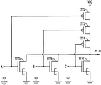
〔論理回路〕
図17は、本主題の種々の実施形態群にかかる、トンネリング・トランジスタを有するNORゲート論理回路を描いてある。入力A, B, C から、示したCMOS論理回路へと論理レベルを導入する。これらのうちのいずれかの入力からの論理low入力信号によって、PMOSトランジスタ 1772-1774 の対応するいずれかがONになり、トンネリング・トランジスタ 1775-1777 の対応するいずれかがOFFになる。論理high入力信号は逆の作用をする。トンネリング・トランジスタ 1775-1777 のいずれかがONになると、出力をground(すなわち論理0)にもってゆく作用が得られる。PMOSトランジスタ 1772-1774 のすべてがONになると、出力をVDD(すなわち論理1)につなぐ作用が得られる。
[Logic circuit]
FIG. 17 depicts a NOR gate logic circuit with tunneling transistors, according to various embodiments of the present subject matter. Introduce logic levels from inputs A, B, and C to the CMOS logic circuit shown. A logic low input signal from any of these inputs turns on one of the corresponding PMOS transistors 1772-1774 and turns off one of the corresponding tunneling transistors 1775-1777. A logic high input signal has the opposite effect. If any of the tunneling transistors 1775-1777 is turned on, the effect is to bring the output to ground (ie logic 0). When all of the PMOS transistors 1772-1774 are turned on, the effect of connecting the output to VDD (ie, logic 1) is obtained.
図18は、本主題の種々の実施形態群にかかる、トンネリング・トランジスタを有するNANDゲート論理回路を描いてある。本出願では、トンネリング・トランジスタをNANDゲートCMOS論理回路内に組み込み、NMOSトランジスタがVssに最近接するようにしている。三つの入力 A, B, C のうちのいずれかからの論理low入力信号によって、PMOS装置 1878-1880 の対応するいずれかがONになり、そして出力を論理highへと押しやる。すべての入力で論理highになると、NMOSトランジスタ 1881-1882 のそれぞれがONになり、そしてトンネリング・トランジスタ 1883 もONになって出力を論理lowに押しやる。
FIG. 18 depicts a NAND gate logic circuit with tunneling transistors, according to various embodiments of the present subject matter. In this application, a tunneling transistor is incorporated into a NAND gate CMOS logic circuit so that the NMOS transistor is closest to Vss. A logic low input signal from any of the three inputs A, B, C turns on the corresponding one of the PMOS devices 1878-1880 and pushes the output to a logic high. When all inputs have a logic high, each of NMOS transistors 1881-1882 is turned on, and
本主題にかかるトンネリング・トランジスタによって、閾値下漏洩電流を実質的に減らすことが可能となり、ひいてはCMOS回路(図17に示したNORゲート論理回路および図18に示したNANDゲート論理回路など)の動作電力も低減できる。本主題にかかるトンネリング・トランジスタは任意のトランジスタ回路に使用できるので、これらの実施形態群は説明のみを目的としたものである。 The tunneling transistor according to the present subject makes it possible to substantially reduce the subthreshold leakage current, and thus the operation of the CMOS circuit (such as the NOR gate logic circuit shown in FIG. 17 and the NAND gate logic circuit shown in FIG. 18). Electric power can also be reduced. Since the tunneling transistor according to the present subject matter can be used in any transistor circuit, these embodiments are for illustrative purposes only.
〔高レベル装置/システム〕
図19は、本主題の種々の実施形態に係るメモリ装置の種々の実施形態を高度に組織化した、単純化したブロック図である。示したメモリ装置 1984 には、メモリアレイ 1985 、および、そのメモリアレイ上での動作を(ひとつもしくは複数の)通信線もしくはチャネル1987 を介して行うための読み込み/書き込み制御回路1986 、が含まれている。示したメモリ装置 1954 としては、メモリカードまたはメモリモジュールを用いることができ、例えばSIMM(single inline memory module)やDIMM(dual inline memory module)などを用いることができる。当業者には、本開示を読んで理解した上で、メモリアレイ内および/もしくは制御回路内の半導体部品を、上述したようなトンネリング・トランジスタを使って組み立てられる、ということがわかるであろう。構造体とこれらの装置の製造方法については上記してある。
[High-level equipment / system]
FIG. 19 is a highly organized, simplified block diagram of various embodiments of memory devices according to various embodiments of the present subject matter. The illustrated
メモリアレイ 1985 は、多数のメモリセル 1988 を有する。アレイになったメモリセルは、行と列をなすように配置される。種々の実施形態群では、ワード線 1989 を行に並んだメモリセルに接続し、またビット線 1990 を列に並んだメモリセルに接続する。読み込み/書き込み制御回路 1986 には、所望の行を選択する機能を持つワード線選択回路 1991 と、所望の列を選択する機能を持つビット線選択回路 1992 と、メモリアレイ 1985 中の選択したメモリセルについてのメモリ状態を検出する機能を持つ読み出し回路 1993 と、が含まれる。
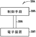
図20には、種々の実施形態群にかかる、(一個もしくは複数個の)トンネリング・トランジスタを持つ電子システムの概要図を示してある。電子システム 2094 には、制御手段 2095 、バス 2096 、および電子装置 2097 が含まれており、このバス2096 が制御手段 2095 と電子装置 2097 との通信回線になっている。種々の実施形態群では、制御手段および/もしくは電子装置に、前述したようなトンネリング・トランジスタが含まれる。示した電子システム 2094 としては、情報処理装置、無線装置、遠隔通信装置、光ファイバー系、電気-光学系、およびコンピュータなどがあるが、これらに限定はされない。
FIG. 20 shows a schematic diagram of an electronic system with tunneling transistor (s) according to various embodiments. The
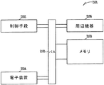
図21は、制御手段 2102 とメモリ 2103 を有するシステム 2101 の或る実施形態の概要図である。この制御手段 2102 および/もしくはメモリ 2103 が、種々の実施形態群にかかるトンネリング・トランジスタを有してもよい。示したシステム 2101 にはまた、電子装置 2104 、ならびに、制御手段と電子装置との間および制御手段とメモリとの間の(ひとつもしくは複数の)通信回線となるバス 2105 、も含まれる。このようなバスとしては、それぞれが独立に構成された、アドレス、データバス、および制御バスを使用する。あるいは、アドレス、データ、かつ/または制御を提供する共通通信回線を使用してもよい。そして、その使用は制御手段によって制御される。或る実施形態では、電子装置 2104 が、メモリ 2103 と同様に構成された付加的なメモリであってもよい。或る実施形態では、バス 2105 に接続した(一個もしくは複数個の)周辺機器 2106 を含んでもよい。そうした周辺機器としては、ディスプレイ、付加的な記憶メモリ、または、制御手段および/もしくはメモリと協働できる他の制御機器、などがある。或る実施形態では、制御手段としてプロセッサを用いる。制御手段 2102 、メモリ 2103 、電子装置 2104 、および周辺機器 2106 のうちのどれでもが、種々の実施形態群に応じて形成されたトンネリング・トランジスタを含んでよい。こうしたシステム 2101 としては、情報処理装置、遠隔通信システム、およびコンピュータがあるが、これらに限定はされない。本開示に記載したトンネリング・トランジスタに関する用途としては、メモリモジュール、装置ドライバ、電力モジュール、通信モデム、プロセッサモジュール、および特定用途モジュールに使うための電子システムが含まれ、ひいては複数レイヤの、複数チップを含むモジュールを含んでもよい。こうした回路が、時計、テレビジョン、携帯電話、PC、自動車、産業用制御システム、飛行機、などのさまざまな電子システムの従属部品であってもよい。
FIG. 21 is a schematic diagram of an embodiment of a
こうしたメモリは、種々の実施形態群にかかる、トンネリング・トランジスタを内包するメモリ装置として実現可能である。実施形態群によって、任意の大きさと種類のメモリ回路と同等の効果が得られ、特定の種類のメモリ装置に限定することは企図していない。メモリの種類としては、DRAM、SRAM(Static Random Access Memory)、もしくはフラッシュメモリがある。さらに云えば、DRAMとして、シンクロナスDRAMを使ってもよいと考えられる。そうしたシンクロナスDRAMのことを、SGRAM(Synchronous Graphics Random Access Memory)、SDRAM(Synchronous Dynamic Random Access Memory)、SDRAM II、およびDDR SDRAM(Double Data Rate SDRAM)とも呼ぶ。さまざまな新興のメモリ技術で、トンネリング・トランジスタを具えたトランジスタを使うこともできる。 Such a memory can be realized as a memory device including a tunneling transistor according to various embodiments. According to the embodiments, an effect equivalent to that of a memory circuit of an arbitrary size and type can be obtained, and it is not intended to limit to a specific type of memory device. Memory types include DRAM, SRAM (Static Random Access Memory), or flash memory. Furthermore, it is considered that a synchronous DRAM may be used as the DRAM. Such synchronous DRAM is also called SGRAM (Synchronous Graphics Random Access Memory), SDRAM (Synchronous Dynamic Random Access Memory), SDRAM II, and DDR SDRAM (Double Data Rate SDRAM). Transistors with tunneling transistors can be used in various emerging memory technologies.
本開示には、いろいろな工程、回路図、およびセル構造体が入っている。本主題は、特定の工程順序もしくは論理配置に限定はされない。特定の実施形態群について本明細書にて図解したが、当業者には、同じ目的を達成するために考案された任意の配置を、示した特定の実施形態に代えて使用できる、ということが正しく理解できるだろう。本出願は、本主題の応用例もしくは変形例を包括せむとするものである。上述の記載は例示を目的としたものであって、限定をしようとするものではないことを理解されたい。上述した実施形態群を組み合わせたものや、その他の実施形態群についても、当業者には上述の記載を通読すれば自明のものとなる。付随する請求項を、その請求項が体現する均等な特徴の全範囲と併せて参照することによって、本主題の範囲を定めるべきである。 The present disclosure includes various processes, circuit diagrams, and cell structures. The present subject matter is not limited to a particular process sequence or logical arrangement. Although illustrated herein for particular embodiments, those skilled in the art will recognize that any arrangement devised to accomplish the same purpose can be used in place of the particular embodiments shown. You will understand correctly. This application is intended to cover applications and variations of the present subject matter. It should be understood that the above description is intended to be illustrative and not restrictive. Those who combine the above-described embodiments and other embodiments will be obvious to those skilled in the art after reading the above description. The scope of the present subject matter should be determined by reference to the appended claims, along with the full scope of equivalent features that they claim.
Claims (71)
前記ナノFinの周りに在る、サラウンディングゲート絶縁体と、
前記ナノFinの周りに前記サラウンディングゲート絶縁体を間に挟んで在る、サラウンディングゲートと、
前記ナノFinの底端に在る第一の導電型を持つ第一のソース/ドレイン領域、および、前記ナノFinの頂端に在る第二の導電型を持つ第二のソース/ドレイン領域と
を含み、ここで、
前記第一のソース/ドレイン領域および前記第二のソース/ドレイン領域が、前記第一のソース/ドレイン領域と前記第二のソース/ドレイン領域との間を垂直方向に走るチャネル領域を劃定する
ことを特徴とする、トランジスタ。 Nano-Fin having a cross-sectional width that is less than or equal to the lithography reference dimension in the first direction and having a cross-sectional width that corresponds to a minimum feature dimension in a second direction perpendicular to the first direction;
Surrounding gate insulator around the nano-Fin,
Surrounding gates sandwiching the surrounding gate insulator around the nano fins, and
A first source / drain region having a first conductivity type at the bottom end of the nano-fin and a second source / drain region having a second conductivity type at the top end of the nano-fin. Including, where
The first source / drain region and the second source / drain region define a channel region that runs vertically between the first source / drain region and the second source / drain region. A transistor characterized by that.
複数の溝が前記結晶質基板にエッチングされて前記ナノFinを劃定する
ことを特徴とする、請求項1記載のトランジスタ。 The nano-fin is formed from a crystalline substrate, and
2. The transistor according to claim 1, wherein a plurality of grooves are etched in the crystalline substrate to determine the nanofin.
前記第二のソース/ドレイン領域が、N+導電型を有する
ことを特徴とする、請求項1記載のトランジスタ。 The first source / drain region has P + conductivity type, and
2. The transistor of claim 1, wherein the second source / drain region has N + conductivity type.
をさらに含む、請求項4記載のトランジスタ。 5. The transistor of claim 4, further comprising a P + conductive line in the crystalline substrate and connected to the first source / drain region.
前記ナノFinの周りにサラウンディングゲート絶縁体を形成するステップと、
前記ナノFinの周りに前記サラウンディングゲート絶縁体を間に挟んでサラウンディングゲート絶縁体を形成するステップと
を含む、トランジスタの形成方法であって、ここで、
前記ナノFinを用いることによって、第一の導電型を持つ第一のソース/ドレイン領域と、第二の導電型を持つ第二のソース/ドレイン領域との間を垂直方向に走るチャネルが得られる
ことを特徴とする、方法。 Forming a nano-Fin having a cross-sectional width that is less than or equal to a lithography reference dimension in a first direction and having a cross-sectional width that corresponds to a minimum feature dimension in a second direction perpendicular to the first direction;
Forming a surrounding gate insulator around the nanofin;
Forming a surrounding gate insulator around the nano-Fin with the surrounding gate insulator interposed therebetween, wherein:
By using the nano-fin, a channel that runs vertically between the first source / drain region having the first conductivity type and the second source / drain region having the second conductivity type is obtained. A method characterized by that.
基板上に非晶質の半導体柱を形成し、前記半導体柱を再結晶して前記ナノFinを形成するステップ
を含む、請求項6記載の方法。 The step of forming nano-fins
7. The method of claim 6, comprising forming amorphous semiconductor pillars on a substrate and recrystallizing the semiconductor pillars to form the nanofins.
結晶質基板に複数の溝をエッチングすることで、前記結晶質基板から前記ナノFinを形成するステップ
を含む、請求項6記載の方法。 The step of forming nano-fins
7. The method of claim 6, comprising forming the nano-Fin from the crystalline substrate by etching a plurality of grooves in the crystalline substrate.
前記第二のソース/ドレイン領域が、N+導電型を有する
ことを特徴とする、請求項6記載の方法。 The first source / drain region has P + conductivity type, and
7. The method of claim 6, wherein the second source / drain region has N + conductivity type.
をさらに含む、請求項9記載の方法。 10. The method of claim 9, further comprising forming a P + conductive line on the substrate and connecting to the first source / drain region.
前記結晶質柱の周りに在る、サラウンディングゲート絶縁体と、
前記結晶質柱の周りに前記サラウンディングゲート絶縁体を間に挟んで在る、サラウンディングゲートと
を含み、ここで、
第一の導電型を持つ第一のソース/ドレイン領域と、第二の導電型を持つ第二のソース/ドレイン領域との間を垂直方向に走るチャネルを得るために、前記結晶質柱が用いられる
ことを特徴とする、トランジスタ。 A crystalline column formed on at least one of the substrate surfaces and having a cross-sectional dimension that is equal to or smaller than a lithography reference dimension,
A surrounding gate insulator around the crystalline pillar; and
A surrounding gate sandwiched around the crystalline pillar with the surrounding gate insulator interposed therebetween, wherein
The crystalline column is used to obtain a channel that runs vertically between a first source / drain region having a first conductivity type and a second source / drain region having a second conductivity type. A transistor, characterized in that
前記第二のソース/ドレイン領域が、N+導電型を有する
ことを特徴とする、請求項11記載のトランジスタ。 The first source / drain region has P + conductivity type, and
12. The transistor according to claim 11, wherein the second source / drain region has N + conductivity type.
をさらに含む、請求項12記載のトランジスタ。 13. The transistor of claim 12, further comprising a P + conductive line in the substrate and connected to the first source / drain region.
基板上に非晶質半導体柱を形成してから、前記非晶質半導体柱を再結晶することで、前記結晶質柱を形成するステップ
を含んだステップと、
サラウンディングゲート絶縁体を、前記結晶質柱の周りに形成するステップと、
サラウンディングゲートを、前記結晶質柱の周りに前記サラウンディングゲート絶縁体を間に挟んで形成するステップと
を含み、ここで、
第一の導電型を有する第一のソース/ドレイン領域と第二の導電型を有する第二のソース/ドレイン領域との間を垂直方向に走るチャネル領域が、前記結晶質柱を用いて得られる
ことを特徴とする、トランジスタの形成方法。 Forming a crystalline column having a cross-sectional dimension that is less than or equal to a lithography reference dimension in at least one direction, comprising:
Forming an amorphous semiconductor pillar on a substrate and then recrystallizing the amorphous semiconductor pillar to form the crystalline pillar; and
Forming a surrounding gate insulator around the crystalline pillar;
Forming a surrounding gate around the crystalline pillar with the surrounding gate insulator interposed therebetween, wherein
A channel region running vertically between a first source / drain region having a first conductivity type and a second source / drain region having a second conductivity type is obtained using the crystalline pillar. A method for forming a transistor.
を形成するステップが、
第一の方向についてリソグラフィ基準寸法以下である断面巾を有し、且つ前記第一の方向に直交する第二の方向について最小フィーチャ寸法に対応する断面巾を有するような、結晶質ナノFinを形成するステップ
を含む、請求項16記載の方法。 Forming a crystalline column having a cross-sectional dimension that is less than or equal to a lithography reference dimension in at least one direction;
Forming crystalline nano-fins having a cross-sectional width that is less than or equal to the lithography reference dimension in the first direction and a cross-sectional width that corresponds to a minimum feature dimension in a second direction orthogonal to the first direction 17. The method of claim 16, comprising the step of:
第一の方向についてリソグラフィ基準寸法以下である断面巾を有し、且つ前記第一の方向に直交する第二の方向について最小フィーチャ寸法に対応する断面巾を有するような、結晶質ナノワイヤを形成するステップ
を含む、請求項16記載の方法。 Forming a crystalline column having a cross-sectional dimension that is less than or equal to a lithography reference dimension in at least one direction;
Forming a crystalline nanowire having a cross-sectional width that is less than or equal to a lithography reference dimension in a first direction and a cross-sectional width that corresponds to a minimum feature dimension in a second direction orthogonal to the first direction; The method of claim 16, comprising steps.
前記第二のソース/ドレイン領域が、N+導電型を有する
ことを特徴とする、請求項16記載の方法。 The first source / drain region has P + conductivity type;
The method of claim 16, wherein the second source / drain region has N + conductivity type.
非晶質半導体材料でできており且つ厚さがリソグラフィ基準寸法以下である柱を、結晶質基板上に形成するステップと、
固相エピタキシー(SPE)工程を使って、前記結晶質基板を種とした結晶成長によって、前記非晶質半導体材料を結晶化するステップと
を含み、ここで前記トランジスタボディは、結晶化した半導体柱の第一の導電型を有する第一のソース/ドレイン領域と第二の導電型を有する第二のソース/ドレイン領域との間につくられる
というステップと、
サラウンディングゲート絶縁体を、前記半導体柱の周りに形成するステップと、
サラウンディングゲートを、前記半導体柱の周りに前記サラウンディングゲート絶縁体を間に挟んで形成するステップと
を含む、トランジスタの形成方法。 Forming a transistor body comprising:
Forming a column made of an amorphous semiconductor material and having a thickness equal to or less than a lithography reference dimension on a crystalline substrate;
Crystallizing the amorphous semiconductor material by crystal growth using the crystalline substrate as a seed using a solid phase epitaxy (SPE) process, wherein the transistor body comprises a crystallized semiconductor pillar A first source / drain region having a first conductivity type and a second source / drain region having a second conductivity type; and
Forming a surrounding gate insulator around the semiconductor pillar;
Forming a surrounding gate around the semiconductor pillar with the surrounding gate insulator interposed therebetween.
非晶質珪素でできている柱を結晶質珪素基板上に形成するステップ
を含む、請求項21記載の方法。 Forming a column made of an amorphous semiconductor material on a crystalline substrate;
23. The method of claim 21, comprising forming a column made of amorphous silicon on a crystalline silicon substrate.
酸化珪素を形成するステップ
を含む、請求項21記載の方法。 Forming the surrounding gate insulator comprises:
The method of claim 21, comprising forming silicon oxide.
ポリシリコンゲートを形成するステップ
を含む、請求項21記載の方法。 The step of forming the surrounding gate is
24. The method of claim 21, comprising forming a polysilicon gate.
金属ゲートを形成するステップ
を含む、請求項21記載の方法。 The step of forming the surrounding gate is
The method of claim 21, comprising forming a metal gate.
をさらに含む、請求項21記載の方法。 24. The method of claim 21, further comprising the step of recessing the surrounding gate such that the height of the surrounding gate is less than the height of the column.
をさらに含む、請求項21記載の方法。 23. The method of claim 21, further comprising forming the first source / drain region in the crystalline substrate and forming the second source / drain region on top of the pillar.
前記結晶質基板中に形成された、第一の導電型を有する第一のソース/ドレイン領域と、
前記結晶質基板上に、前記第一のソース/ドレイン領域と接続するようにして形成され、且つ断面寸法が最小フィーチャ寸法未満である、結晶質半導体柱と、
前記柱の頂部に形成された、第二の導電型を有する第二のソース/ドレイン領域と、
前記柱の周りに形成された、ゲート絶縁体と、
前記柱の周りに前記ゲート絶縁体を間に挟んで形成された、サラウンディングゲートと
を含む、トランジスタ。 A crystalline substrate;
A first source / drain region having a first conductivity type formed in the crystalline substrate;
A crystalline semiconductor pillar formed on the crystalline substrate to connect to the first source / drain region and having a cross-sectional dimension less than a minimum feature dimension;
A second source / drain region having a second conductivity type formed at the top of the column;
A gate insulator formed around the pillar;
And a surrounding gate formed around the pillar with the gate insulator interposed therebetween.
非晶質半導体材料でできており且つ断面厚さが最小フィーチャ寸法未満であるFinを、結晶質基板上に形成するステップと、
固相エピタキシー(SPE)工程を使って、前記結晶質基板を種とした結晶成長によって、前記非晶質半導体材料を結晶化するステップと
を含み、ここで前記トランジスタボディは、結晶化した半導体柱の第一の導電型を有する第一のソース/ドレイン領域と第二の導電型を有する第二のソース/ドレイン領域との間につくられる
というステップと、
サラウンディングゲート絶縁体を、前記半導体柱の周りに形成するステップと、
サラウンディングゲートを、前記半導体柱の周りに前記サラウンディングゲート絶縁体を間に挟んで形成するステップと
を含む、トランジスタの形成方法。 Forming a transistor body comprising:
Forming a Fin made of an amorphous semiconductor material and having a cross-sectional thickness less than a minimum feature size on a crystalline substrate;
Crystallizing the amorphous semiconductor material by crystal growth using the crystalline substrate as a seed using a solid phase epitaxy (SPE) process, wherein the transistor body comprises a crystallized semiconductor pillar A first source / drain region having a first conductivity type and a second source / drain region having a second conductivity type; and
Forming a surrounding gate insulator around the semiconductor pillar;
Forming a surrounding gate around the semiconductor pillar with the surrounding gate insulator interposed therebetween.
前記Finの前記第一の方向に直交する第二の方向についての断面厚さが、前記最小フィーチャ長未満である
ことを特徴とする、請求項34記載の方法。 The cross-sectional thickness in the first direction of the Fin corresponds to a minimum feature length, and
35. The method of claim 34, wherein a cross-sectional thickness of the Fin in a second direction orthogonal to the first direction is less than the minimum feature length.
結晶質珪素基板上に非晶質珪素の柱を形成するステップ
を含む、請求項34記載の方法。 Forming a Fin made of an amorphous semiconductor material on a crystalline substrate;
35. The method of claim 34, comprising forming amorphous silicon pillars on the crystalline silicon substrate.
酸化珪素を形成するステップ
を含む、請求項34記載の方法。 Forming the surrounding gate insulator comprises:
35. The method of claim 34, comprising forming silicon oxide.
ポリシリコンゲートを形成するステップ
を含む、請求項34記載の方法。 The step of forming the surrounding gate is
35. The method of claim 34, comprising forming a polysilicon gate.
をさらに含む、請求項34記載の方法。 35. The method of claim 34, further comprising indenting the surrounding gate such that the height of the surrounding gate is less than the height of the Fin.
をさらに含む、請求項34記載の方法。 Forming the first source / drain region with a P + region at the first end of the Fin and forming the second source / drain region with an N + region at the second end of the Fin. 35. The method of claim 34, further comprising:
チャネル領域が前記第一のソース/ドレイン領域と前記第二のソース/ドレイン領域との間を垂直方向に走っている
ことを特徴とする、請求項40記載の方法。 The first source / drain region is below the second source / drain region;
41. The method of claim 40, wherein a channel region runs vertically between the first source / drain region and the second source / drain region.
前記結晶質基板上に在り、且つ断面寸法が最小フィーチャ寸法未満であり、且つ第一の導電型を有する下部ソース/ドレイン領域と第二の導電型を有する上部ソース/ドレイン領域との間を垂直に走るチャネルを与える、結晶質半導体Finと、
前記結晶質半導体Finの周りに形成された、ゲート絶縁体と、
前記結晶質半導体Finの周りに前記ゲート絶縁体を間に挟んで形成された、サラウンディングゲートと
を含む、トランジスタ。 A crystalline substrate;
A vertical cross-section between a lower source / drain region having a first conductivity type and an upper source / drain region having a second conductivity type on the crystalline substrate and having a cross-sectional dimension less than a minimum feature dimension. A crystalline semiconductor Fin that gives the channel to run,
A gate insulator formed around the crystalline semiconductor Fin;
A transistor comprising a surrounding gate formed around the crystalline semiconductor Fin with the gate insulator interposed therebetween.
前記上部ソース/ドレイン領域が、N+導電型を有する
ことを特徴とする、請求項42記載のトランジスタ。 The lower source / drain region has P + conductivity type;
43. The transistor of claim 42, wherein the upper source / drain region has N + conductivity type.
をさらに含む、請求項47記載のトランジスタ。 48. The transistor of claim 47, further comprising a P + conductive line formed in the crystalline substrate and connected to the lower source / drain region.
第一の導電型を有する第一のソース/ドレイン領域を、前記結晶質基板内の前記Finの下方に形成するステップと、
サラウンディングゲート絶縁体を、前記Finの周りに形成するステップと、
サラウンディングゲートを、前記Finの周りに前記サラウンディングゲート絶縁体を間に挟んで形成するステップと、
第二の導電型を有する第二のソース/ドレイン領域を、前記Finの頂部に形成するステップと
を含む、トランジスタの形成方法。 Forming Fin from a crystalline substrate;
Forming a first source / drain region having a first conductivity type below the Fin in the crystalline substrate;
Forming a surrounding gate insulator around the Fin;
Forming a surrounding gate around the Fin with the surrounding gate insulator interposed therebetween;
Forming a second source / drain region having a second conductivity type on the top of the Fin.
前記第二のソース/ドレイン領域が、N+導電型を有する
ことを特徴とする、請求項49記載の方法。 The first source / drain region has P + conductivity type;
50. The method of claim 49, wherein the second source / drain region has N + conductivity type.
をさらに含む、請求項50記載の方法。 51. The method of claim 50, further comprising a P + conductive line formed in the crystalline substrate and connected to the first source / drain region.
前記Finの前記第一の方向に直交する第二の方向についての断面厚さが、前記最小フィーチャ長未満である
ことを特徴とする、請求項49記載の方法。 The cross-sectional thickness in the first direction of the Fin corresponds to a minimum feature length, and
50. The method of claim 49, wherein a cross-sectional thickness of the Fin in a second direction orthogonal to the first direction is less than the minimum feature length.
結晶質珪素基板からFinを形成するステップ
を含む、請求項49記載の方法。 Forming Fin from the crystalline substrate comprises:
50. The method of claim 49, comprising forming Fin from a crystalline silicon substrate.
前記結晶質基板をエッチングすることでFinを形成するステップ
を含む、請求項49記載の方法。 Forming Fin from the crystalline substrate comprises:
50. The method of claim 49, comprising etching the crystalline substrate to form a Fin.
前記結晶質基板に隣接する溝へドーパントを注入し、前記ドーパントを前記Finの下部に拡散させるステップ
を含む、請求項49記載の方法。 Forming a first source / drain region below the Fin in the crystalline substrate;
50. The method of claim 49, comprising implanting a dopant into a trench adjacent to the crystalline substrate and diffusing the dopant below the Fin.
前記ドーパントを前記Finの底部へと拡散させるステップ
を含む、請求項55記載の方法。 The spreading step is
56. The method of claim 55, comprising diffusing the dopant into the bottom of the Fin.
酸化珪素を形成するステップ
を含む、請求項49記載の方法。 Forming the surrounding gate insulator comprises:
50. The method of claim 49, comprising forming silicon oxide.
ポリシリコンゲートを形成するステップ
を含む、請求項49記載の方法。 The step of forming the surrounding gate is
50. The method of claim 49, comprising forming a polysilicon gate.
をさらに含む、請求項49記載の方法。 50. The method of claim 49, further comprising indenting the surrounding gate such that the height of the surrounding gate is less than the height of the Fin.
をさらに含む、請求項49記載の方法。 50. The method of claim 49, further comprising forming a gate contact to connect adjacent to the surrounding gate.
をさらに含む、請求項49記載の方法。 50. The method of claim 49, further comprising forming at least one gate line to connect adjacent to the surrounding gate.
第一のゲート線を前記サラウンディングゲートの第一の側に隣接して接続するように形成し、第二のゲート線を前記サラウンディングゲートの第二の側に隣接して接続するように形成し、ここで前記第一の側と前記第二の側が、前記Finの対向する側部にそれぞれ位置しているステップ
を含む、請求項61記載の方法。 Forming at least one gate line adjacent to the surrounding gate;
A first gate line is formed adjacent to the first side of the surrounding gate, and a second gate line is formed adjacent to the second side of the surrounding gate. 62. The method of claim 61, further comprising the step of wherein the first side and the second side are respectively located on opposite sides of the Fin.
少なくともひとつのゲート線を前記サラウンディングゲートに隣接して接続するように形成するステップが、
前記長辺上で前記サラウンディングゲートに接続するようにゲート線を形成するステップ
を含む
ことを特徴とする、請求項61記載の方法。 The occupied area of the Fin is a rectangle having a short side and a long side, and
Forming at least one gate line adjacent to the surrounding gate;
62. The method of claim 61, comprising forming a gate line to connect to the surrounding gate on the long side.
少なくともひとつのゲート線を前記サラウンディングゲートに隣接して接続するように形成するステップが、
前記短辺上で前記サラウンディングゲートに接続するようにゲート線を形成するステップ
を含む
ことを特徴とする、請求項61記載の方法。 The occupied area of the Fin is a rectangle having a short side and a long side, and
Forming at least one gate line adjacent to the surrounding gate;
62. The method of claim 61, comprising forming a gate line to connect to the surrounding gate on the short side.
ポリシリコンサラウンディングゲートを形成するステップ
を含む、請求項49記載の方法。 The step of forming the surrounding gate is
50. The method of claim 49, comprising forming a polysilicon surrounding gate.
前記結晶質基板内の前記結晶質半導体Finの底部に形成された第一の導電型を有する第一のソース/ドレイン領域、および、前記結晶質半導体Finの頂部に形成された第二の導電型を有する第二のソース/ドレイン領域と、
前記結晶質半導体Finの周りに形成された、ゲート絶縁体と、
前記結晶質半導体Finの周りに前記ゲート絶縁体を間に挟んで形成された、サラウンディングゲートと
を含み、ここで、
前記第一のソース/ドレイン領域および前記第二のソース/ドレイン領域が、前記結晶質半導体Fin内の前記第一のソース/ドレイン領域と前記第二のソース/ドレイン領域との間に垂直方向に走るチャネル領域を劃定する
ことを特徴とする、トランジスタ。 A crystalline substrate in which a crystalline semiconductor Fin having a cross-sectional dimension that is less than a minimum feature dimension is produced by etching a groove; and
A first source / drain region having a first conductivity type formed at the bottom of the crystalline semiconductor Fin in the crystalline substrate; and a second conductivity type formed at the top of the crystalline semiconductor Fin. A second source / drain region having
A gate insulator formed around the crystalline semiconductor Fin;
A surrounding gate formed around the crystalline semiconductor Fin with the gate insulator interposed therebetween, wherein
The first source / drain region and the second source / drain region are perpendicular to each other between the first source / drain region and the second source / drain region in the crystalline semiconductor Fin. A transistor characterized by determining a channel region in which it runs.
Applications Claiming Priority (6)
| Application Number | Priority Date | Filing Date | Title |
|---|---|---|---|
| US11/397,406 US20070228491A1 (en) | 2006-04-04 | 2006-04-04 | Tunneling transistor with sublithographic channel |
| US11/397,413 US7491995B2 (en) | 2006-04-04 | 2006-04-04 | DRAM with nanofin transistors |
| US11/397,527 US7425491B2 (en) | 2006-04-04 | 2006-04-04 | Nanowire transistor with surrounding gate |
| US11/397,430 US8734583B2 (en) | 2006-04-04 | 2006-04-04 | Grown nanofin transistors |
| US11/397,358 US8354311B2 (en) | 2006-04-04 | 2006-04-04 | Method for forming nanofin transistors |
| PCT/US2007/008124 WO2007120493A1 (en) | 2006-04-04 | 2007-04-03 | Nanofin tunneling transistors |
Publications (1)
| Publication Number | Publication Date |
|---|---|
| JP2009532905A true JP2009532905A (en) | 2009-09-10 |
Family
ID=38325217
Family Applications (4)
| Application Number | Title | Priority Date | Filing Date |
|---|---|---|---|
| JP2009504239A Withdrawn JP2009532905A (en) | 2006-04-04 | 2007-04-03 | Nano Fin Tunneling Transistor |
| JP2009504280A Active JP5234439B2 (en) | 2006-04-04 | 2007-04-03 | Nano Fin transistor made by etching |
| JP2009504232A Active JP5229587B2 (en) | 2006-04-04 | 2007-04-03 | Growth type nano fin transistor |
| JP2009504238A Active JP5229635B2 (en) | 2006-04-04 | 2007-04-03 | Nanowire transistor with surrounding gate |
Family Applications After (3)
| Application Number | Title | Priority Date | Filing Date |
|---|---|---|---|
| JP2009504280A Active JP5234439B2 (en) | 2006-04-04 | 2007-04-03 | Nano Fin transistor made by etching |
| JP2009504232A Active JP5229587B2 (en) | 2006-04-04 | 2007-04-03 | Growth type nano fin transistor |
| JP2009504238A Active JP5229635B2 (en) | 2006-04-04 | 2007-04-03 | Nanowire transistor with surrounding gate |
Country Status (5)
| Country | Link |
|---|---|
| EP (4) | EP2002470B1 (en) |
| JP (4) | JP2009532905A (en) |
| KR (5) | KR20090006169A (en) |
| SG (2) | SG170827A1 (en) |
| WO (4) | WO2007136461A2 (en) |
Cited By (6)
| Publication number | Priority date | Publication date | Assignee | Title |
|---|---|---|---|---|
| JP2014013893A (en) * | 2012-06-15 | 2014-01-23 | Imec | Tunnel field effect transistor device and method for making said device |
| JP2014120777A (en) * | 2012-12-17 | 2014-06-30 | Kyungpook National Univ Industry-Academic Cooperation Foundation | Tunneling field effect transistor and method of manufacturing tunneling field effect transistor |
| JP2015050196A (en) * | 2013-08-29 | 2015-03-16 | 株式会社東芝 | Semiconductor device |
| JP2016534572A (en) * | 2013-09-09 | 2016-11-04 | クアルコム,インコーポレイテッド | Vertical tunnel field effect transistor |
| JP2020519019A (en) * | 2017-05-01 | 2020-06-25 | アドバンスト・マイクロ・ディバイシズ・インコーポレイテッドAdvanced Micro Devices Incorporated | Vertical Gate All Around Library Architecture |
| JP2021507519A (en) * | 2017-12-21 | 2021-02-22 | インターナショナル・ビジネス・マシーンズ・コーポレーションInternational Business Machines Corporation | How to Form Semiconductor Devices and Semiconductor Devices |
Families Citing this family (22)
| Publication number | Priority date | Publication date | Assignee | Title |
|---|---|---|---|---|
| KR100790863B1 (en) * | 2005-12-28 | 2008-01-03 | 삼성전자주식회사 | Nano wire manufacturing method |
| US8734583B2 (en) | 2006-04-04 | 2014-05-27 | Micron Technology, Inc. | Grown nanofin transistors |
| US8354311B2 (en) | 2006-04-04 | 2013-01-15 | Micron Technology, Inc. | Method for forming nanofin transistors |
| US7491995B2 (en) | 2006-04-04 | 2009-02-17 | Micron Technology, Inc. | DRAM with nanofin transistors |
| US7425491B2 (en) | 2006-04-04 | 2008-09-16 | Micron Technology, Inc. | Nanowire transistor with surrounding gate |
| US8643087B2 (en) | 2006-09-20 | 2014-02-04 | Micron Technology, Inc. | Reduced leakage memory cells |
| KR100945511B1 (en) * | 2008-04-10 | 2010-03-09 | 주식회사 하이닉스반도체 | Semiconductor device and manufacturing method thereof |
| US7897494B2 (en) * | 2008-06-24 | 2011-03-01 | Imec | Formation of single crystal semiconductor nanowires |
| DE102009024311A1 (en) * | 2009-06-05 | 2011-01-05 | Fraunhofer-Gesellschaft zur Förderung der angewandten Forschung e.V. | Semiconductor component and method for its production |
| KR101656970B1 (en) | 2011-12-20 | 2016-09-12 | 인텔 코포레이션 | Semiconductor device with isolated body portion |
| KR20130131708A (en) | 2012-05-24 | 2013-12-04 | 에스케이하이닉스 주식회사 | Memory cell array and variable resistive memory device |
| US9006810B2 (en) * | 2012-06-07 | 2015-04-14 | International Business Machines Corporation | DRAM with a nanowire access transistor |
| JP5595619B2 (en) * | 2012-08-08 | 2014-09-24 | ユニサンティス エレクトロニクス シンガポール プライベート リミテッド | Semiconductor device manufacturing method and semiconductor device |
| KR20140040543A (en) * | 2012-09-26 | 2014-04-03 | 삼성전자주식회사 | Fin sturctured field effect transistor, memory device including the same and semiconductor device thereof |
| CN106170867B (en) | 2014-03-28 | 2020-02-14 | 英特尔公司 | Selectively regrown top contact for vertical type semiconductor devices |
| US9941394B2 (en) | 2014-04-30 | 2018-04-10 | Taiwan Semiconductor Manufacturing Co., Ltd. | Tunnel field-effect transistor |
| US9673209B2 (en) | 2014-05-16 | 2017-06-06 | Taiwan Semiconductor Manufacturing Company, Ltd. | Memory device and method for fabricating the same |
| EP3155643B1 (en) * | 2014-06-13 | 2020-10-21 | Intel Corporation | Vertical channel transistors fabrication process by selective subtraction of a regular grid |
| US9818877B2 (en) | 2014-09-18 | 2017-11-14 | International Business Machines Corporation | Embedded source/drain structure for tall finFET and method of formation |
| US10559690B2 (en) | 2014-09-18 | 2020-02-11 | International Business Machines Corporation | Embedded source/drain structure for tall FinFET and method of formation |
| US9634084B1 (en) | 2016-02-10 | 2017-04-25 | Globalfoundries Inc. | Conformal buffer layer in source and drain regions of fin-type transistors |
| KR102593708B1 (en) * | 2018-08-14 | 2023-10-26 | 삼성전자주식회사 | Semiconductor devices and manufacturing methods of the same |
Family Cites Families (33)
| Publication number | Priority date | Publication date | Assignee | Title |
|---|---|---|---|---|
| US4941026A (en) * | 1986-12-05 | 1990-07-10 | General Electric Company | Semiconductor devices exhibiting minimum on-resistance |
| JPH07112067B2 (en) * | 1990-01-24 | 1995-11-29 | 株式会社東芝 | Semiconductor device |
| US5013680A (en) * | 1990-07-18 | 1991-05-07 | Micron Technology, Inc. | Process for fabricating a DRAM array having feature widths that transcend the resolution limit of available photolithography |
| JP3202223B2 (en) * | 1990-11-27 | 2001-08-27 | 日本電気株式会社 | Method for manufacturing transistor |
| JP3219307B2 (en) * | 1991-08-28 | 2001-10-15 | シャープ株式会社 | Semiconductor device structure and manufacturing method |
| JPH05160408A (en) * | 1991-12-04 | 1993-06-25 | Toshiba Corp | Field effect transistor and dynamic semiconductor storage device using same |
| JP3321788B2 (en) * | 1994-05-06 | 2002-09-09 | ソニー株式会社 | MIS type semiconductor device and method of manufacturing the same |
| JP3246196B2 (en) * | 1994-07-13 | 2002-01-15 | ソニー株式会社 | Method of forming quantum wire device |
| JP4047098B2 (en) * | 1994-09-13 | 2008-02-13 | 株式会社東芝 | Semiconductor device and manufacturing method thereof |
| US5990509A (en) * | 1997-01-22 | 1999-11-23 | International Business Machines Corporation | 2F-square memory cell for gigabit memory applications |
| US6063688A (en) * | 1997-09-29 | 2000-05-16 | Intel Corporation | Fabrication of deep submicron structures and quantum wire transistors using hard-mask transistor width definition |
| US6747313B1 (en) * | 1997-12-17 | 2004-06-08 | Hyundai Electronics Industries Co., Ltd. | Thin film transistor |
| DE19943390A1 (en) * | 1999-09-10 | 2001-05-03 | Walter Hansch | Semiconductor component comprises vertical stack comprising source, drain and intermediate layer, gate comprising insulating and conducting layer connecting source and drain and tunnel current flowing in section of gate |
| US6967140B2 (en) * | 2000-03-01 | 2005-11-22 | Intel Corporation | Quantum wire gate device and method of making same |
| US6413802B1 (en) * | 2000-10-23 | 2002-07-02 | The Regents Of The University Of California | Finfet transistor structures having a double gate channel extending vertically from a substrate and methods of manufacture |
| US6664143B2 (en) * | 2000-11-22 | 2003-12-16 | North Carolina State University | Methods of fabricating vertical field effect transistors by conformal channel layer deposition on sidewalls |
| US6531727B2 (en) * | 2001-02-09 | 2003-03-11 | Micron Technology, Inc. | Open bit line DRAM with ultra thin body transistors |
| FR2823009B1 (en) * | 2001-04-02 | 2004-07-09 | St Microelectronics Sa | METHOD FOR MANUFACTURING A VERTICAL TRANSISTOR WITH INSULATED GRID WITH LOW COVERAGE OF THE GRID ON THE SOURCE AND ON THE DRAIN, AND INTEGRATED CIRCUIT COMPRISING SUCH A TRANSISTOR |
| US20030008515A1 (en) * | 2001-07-03 | 2003-01-09 | Tai-Ju Chen | Method of fabricating a vertical MOS transistor |
| US6815750B1 (en) * | 2002-05-22 | 2004-11-09 | Hewlett-Packard Development Company, L.P. | Field effect transistor with channel extending through layers on a substrate |
| US6821834B2 (en) * | 2002-12-04 | 2004-11-23 | Yoshiyuki Ando | Ion implantation methods and transistor cell layout for fin type transistors |
| US6794718B2 (en) * | 2002-12-19 | 2004-09-21 | International Business Machines Corporation | High mobility crystalline planes in double-gate CMOS technology |
| JP4108537B2 (en) * | 2003-05-28 | 2008-06-25 | 富士雄 舛岡 | Semiconductor device |
| US6855582B1 (en) * | 2003-06-12 | 2005-02-15 | Advanced Micro Devices, Inc. | FinFET gate formation using reverse trim and oxide polish |
| JP2005116969A (en) * | 2003-10-10 | 2005-04-28 | Toshiba Corp | Semiconductor device and manufacturing method thereof |
| US7348243B2 (en) * | 2003-12-27 | 2008-03-25 | Dongbu Electronics Co., Ltd. | Semiconductor device and method for fabricating the same |
| US7683428B2 (en) * | 2004-01-22 | 2010-03-23 | International Business Machines Corporation | Vertical Fin-FET MOS devices |
| US7122425B2 (en) * | 2004-08-24 | 2006-10-17 | Micron Technology, Inc. | Methods of forming semiconductor constructions |
| US7242057B2 (en) * | 2004-08-26 | 2007-07-10 | Micron Technology, Inc. | Vertical transistor structures having vertical-surrounding-gates with self-aligned features |
| US7241655B2 (en) * | 2004-08-30 | 2007-07-10 | Micron Technology, Inc. | Method of fabricating a vertical wrap-around-gate field-effect-transistor for high density, low voltage logic and memory array |
| US7910288B2 (en) * | 2004-09-01 | 2011-03-22 | Micron Technology, Inc. | Mask material conversion |
| JP3764161B2 (en) * | 2004-09-17 | 2006-04-05 | 株式会社半導体エネルギー研究所 | Semiconductor device and manufacturing method thereof |
| DE102005045078B4 (en) * | 2004-09-25 | 2009-01-22 | Samsung Electronics Co., Ltd., Suwon | Field effect transistor with a strained channel layer on sidewalls of a structure on a semiconductor substrate |
-
2007
- 2007-04-03 SG SG201102381-9A patent/SG170827A1/en unknown
- 2007-04-03 JP JP2009504239A patent/JP2009532905A/en not_active Withdrawn
- 2007-04-03 JP JP2009504280A patent/JP5234439B2/en active Active
- 2007-04-03 KR KR1020087027075A patent/KR20090006169A/en not_active Ceased
- 2007-04-03 WO PCT/US2007/008084 patent/WO2007136461A2/en not_active Ceased
- 2007-04-03 WO PCT/US2007/008124 patent/WO2007120493A1/en not_active Ceased
- 2007-04-03 SG SG2011038726A patent/SG172643A1/en unknown
- 2007-04-03 EP EP07809002.4A patent/EP2002470B1/en active Active
- 2007-04-03 EP EP07754850A patent/EP2008309A1/en not_active Ceased
- 2007-04-03 WO PCT/US2007/008400 patent/WO2007114927A1/en not_active Ceased
- 2007-04-03 KR KR1020087026970A patent/KR20090007393A/en not_active Withdrawn
- 2007-04-03 WO PCT/US2007/008123 patent/WO2007120492A1/en not_active Ceased
- 2007-04-03 EP EP07754622A patent/EP2002469A1/en not_active Withdrawn
- 2007-04-03 JP JP2009504232A patent/JP5229587B2/en active Active
- 2007-04-03 KR KR1020147009477A patent/KR20140051463A/en not_active Ceased
- 2007-04-03 JP JP2009504238A patent/JP5229635B2/en active Active
- 2007-04-03 EP EP07754621.6A patent/EP2002468B1/en not_active Not-in-force
-
2008
- 2008-11-03 KR KR1020087026973A patent/KR101474028B1/en active Active
- 2008-11-04 KR KR1020087027077A patent/KR101378256B1/en active Active
Cited By (10)
| Publication number | Priority date | Publication date | Assignee | Title |
|---|---|---|---|---|
| JP2014013893A (en) * | 2012-06-15 | 2014-01-23 | Imec | Tunnel field effect transistor device and method for making said device |
| JP2014120777A (en) * | 2012-12-17 | 2014-06-30 | Kyungpook National Univ Industry-Academic Cooperation Foundation | Tunneling field effect transistor and method of manufacturing tunneling field effect transistor |
| JP2015050196A (en) * | 2013-08-29 | 2015-03-16 | 株式会社東芝 | Semiconductor device |
| JP2016534572A (en) * | 2013-09-09 | 2016-11-04 | クアルコム,インコーポレイテッド | Vertical tunnel field effect transistor |
| JP2020519019A (en) * | 2017-05-01 | 2020-06-25 | アドバンスト・マイクロ・ディバイシズ・インコーポレイテッドAdvanced Micro Devices Incorporated | Vertical Gate All Around Library Architecture |
| JP7343395B2 (en) | 2017-05-01 | 2023-09-12 | アドバンスト・マイクロ・ディバイシズ・インコーポレイテッド | Vertical gate all-around library architecture |
| JP2021507519A (en) * | 2017-12-21 | 2021-02-22 | インターナショナル・ビジネス・マシーンズ・コーポレーションInternational Business Machines Corporation | How to Form Semiconductor Devices and Semiconductor Devices |
| JP7355393B2 (en) | 2017-12-21 | 2023-10-03 | インターナショナル・ビジネス・マシーンズ・コーポレーション | Methods of forming semiconductor devices and semiconductor devices |
| US11855149B2 (en) | 2017-12-21 | 2023-12-26 | International Business Machines Corporation | Field effect transistor with controllable resistance |
| US12015056B2 (en) | 2017-12-21 | 2024-06-18 | International Business Machines Corporation | Field effect transistor with controllable resistance |
Also Published As
| Publication number | Publication date |
|---|---|
| WO2007114927A1 (en) | 2007-10-11 |
| KR20090006169A (en) | 2009-01-14 |
| JP5229635B2 (en) | 2013-07-03 |
| KR101474028B1 (en) | 2014-12-17 |
| KR20140051463A (en) | 2014-04-30 |
| EP2002468B1 (en) | 2013-07-24 |
| KR20090005149A (en) | 2009-01-12 |
| JP2009532903A (en) | 2009-09-10 |
| EP2008309A1 (en) | 2008-12-31 |
| WO2007136461A3 (en) | 2008-01-17 |
| JP5234439B2 (en) | 2013-07-10 |
| EP2002468A1 (en) | 2008-12-17 |
| WO2007120493A1 (en) | 2007-10-25 |
| SG170827A1 (en) | 2011-05-30 |
| EP2002470A2 (en) | 2008-12-17 |
| KR20090007393A (en) | 2009-01-16 |
| JP2009532907A (en) | 2009-09-10 |
| KR101378256B1 (en) | 2014-03-25 |
| WO2007136461A2 (en) | 2007-11-29 |
| JP2009532904A (en) | 2009-09-10 |
| EP2002470B1 (en) | 2016-03-09 |
| SG172643A1 (en) | 2011-07-28 |
| EP2002469A1 (en) | 2008-12-17 |
| KR20090007397A (en) | 2009-01-16 |
| JP5229587B2 (en) | 2013-07-03 |
| WO2007120492A1 (en) | 2007-10-25 |
Similar Documents
| Publication | Publication Date | Title |
|---|---|---|
| JP2009532905A (en) | Nano Fin Tunneling Transistor | |
| CN101416317B (en) | Etched nanofin transistors | |
| US9893072B2 (en) | DRAM with nanofin transistors | |
| US20070228491A1 (en) | Tunneling transistor with sublithographic channel | |
| US8823006B2 (en) | Nanofin transistors with crystalline semiconductor fins |
Legal Events
| Date | Code | Title | Description |
|---|---|---|---|
| A300 | Application deemed to be withdrawn because no request for examination was validly filed |
Free format text: JAPANESE INTERMEDIATE CODE: A300 Effective date: 20100706 |