JP2009531710A - Sensor array control circuit and associated method - Google Patents
Sensor array control circuit and associated method Download PDFInfo
- Publication number
- JP2009531710A JP2009531710A JP2009502804A JP2009502804A JP2009531710A JP 2009531710 A JP2009531710 A JP 2009531710A JP 2009502804 A JP2009502804 A JP 2009502804A JP 2009502804 A JP2009502804 A JP 2009502804A JP 2009531710 A JP2009531710 A JP 2009531710A
- Authority
- JP
- Japan
- Prior art keywords
- pressure
- force
- array
- sensor
- sensor element
- Prior art date
- Legal status (The legal status is an assumption and is not a legal conclusion. Google has not performed a legal analysis and makes no representation as to the accuracy of the status listed.)
- Pending
Links
Images


Classifications
-
- G—PHYSICS
- G01—MEASURING; TESTING
- G01L—MEASURING FORCE, STRESS, TORQUE, WORK, MECHANICAL POWER, MECHANICAL EFFICIENCY, OR FLUID PRESSURE
- G01L1/00—Measuring force or stress, in general
- G01L1/20—Measuring force or stress, in general by measuring variations in ohmic resistance of solid materials or of electrically-conductive fluids; by making use of electrokinetic cells, i.e. liquid-containing cells wherein an electrical potential is produced or varied upon the application of stress
- G01L1/205—Measuring force or stress, in general by measuring variations in ohmic resistance of solid materials or of electrically-conductive fluids; by making use of electrokinetic cells, i.e. liquid-containing cells wherein an electrical potential is produced or varied upon the application of stress using distributed sensing elements
Landscapes
- Physics & Mathematics (AREA)
- General Physics & Mathematics (AREA)
- Force Measurement Appropriate To Specific Purposes (AREA)
Abstract
圧力又は力応答センサアレイを走査する制御回路が開示される。圧力又は力応答センサ素子のアレイで形成される圧力センサ又は力センサを使用して、負荷印加に応答して圧力測定又は力測定を得ることができる。制御回路は、センサ素子からの信号をサンプリングして、センサアレイの1つ又は複数のセンサ素子での圧力又は力を検出することができる。本明細書における回路は、比較的より高速の走査速度を提供することができる。ユーザは、センサアレイのセンサ素子の走査対象となる1つ又は複数のサブセットを定義することができる。センサ特性を調整する様々な方法及び関連回路も開示される。 A control circuit for scanning the pressure or force responsive sensor array is disclosed. A pressure sensor or force sensor formed by an array of pressure or force response sensor elements can be used to obtain a pressure measurement or force measurement in response to a load application. The control circuit can sample the signal from the sensor element to detect pressure or force at one or more sensor elements of the sensor array. The circuitry herein can provide a relatively faster scan rate. The user can define one or more subsets to be scanned for sensor elements of the sensor array. Various methods and associated circuitry for adjusting sensor characteristics are also disclosed.
Description
本発明の態様は、圧力又は力応答センサ素子のアレイから形成される圧力センサ又は力センサに関し、特に、このようなアレイを走査する回路に関する。 Aspects of the invention relate to pressure or force sensors formed from arrays of pressure or force responsive sensor elements, and more particularly to circuitry for scanning such arrays.
圧力又は力応答センサ素子アレイで形成される圧力センサ又は力センサは、印加された負荷に応答して圧力測定又は力測定を得るために使用することができる。このようなアレイは、例えば、歯科咬合用の接触センサとして、靴の中の足の圧力を検出するため、ガスケット上の圧力分布又は力分布を検出するために、及び領域上の圧力又は力の分布についての情報が望まれる他の多くの用途で使用することができる。このようなアレイは通常、平行する1組の電極がそれぞれ形成される2つの層を利用し、1組の電極のうちの少なくとも一方の電極が、可変抵抗圧力又は力感応材料(例えば、インク)或いは他の圧力又は力感応材料(例えば、可変容量材料)で覆われる。こういったアレイは、一方の層の電極が他方の層の電極と交差した状態で共に固定することができ、それにより、センサ素子が形成される。各センサ素子を通過する電流を感知することにより、素子での圧力又は力を測定することができる。 A pressure sensor or force sensor formed with an array of pressure or force response sensor elements can be used to obtain a pressure measurement or force measurement in response to an applied load. Such an array can be used, for example, as a contact sensor for dental occlusion, for detecting foot pressure in a shoe, for detecting pressure distribution or force distribution on a gasket, and for pressure or force on an area. It can be used in many other applications where information about the distribution is desired. Such arrays typically utilize two layers, each of which is formed with a parallel set of electrodes, at least one of which is a variable resistance pressure or force sensitive material (eg, ink). Alternatively, it is covered with other pressure or force sensitive materials (eg, variable volume materials). Such arrays can be secured together with one layer of electrodes intersecting the other layer of electrodes, thereby forming a sensor element. By sensing the current passing through each sensor element, the pressure or force at the element can be measured.
各種実施形態では、圧力又は力応答センサ素子アレイを走査する回路及び関連する方法であって、圧力又は力応答センサ素子アレイの走査に使用される従来の回路と比較して、より高い精度及び/又はより高速の走査速度を提供することができる回路及び関連する方法が提供される。いくつかの実施形態では、より高い精度は、圧力又は力応答センサ素子アレイの走査に使用される従来の回路を使用して得られる測定と比較して、圧力又は力応答センサ素子に印加される圧力又は力のより正確な値を測定することを含む。 In various embodiments, circuitry and associated methods for scanning a pressure or force responsive sensor element array, with higher accuracy and / or relative to conventional circuitry used to scan a pressure or force responsive sensor element array. Alternatively, circuits and associated methods are provided that can provide faster scanning speeds. In some embodiments, higher accuracy is applied to the pressure or force responsive sensor elements as compared to measurements obtained using conventional circuitry used to scan the pressure or force responsive sensor element arrays. Including measuring more accurate values of pressure or force.
例示的な一実施形態では、圧力又は力応答センサ素子アレイを走査するための回路が提供される。回路は、圧力又は力応答センサ素子の走査を制御する制御回路を備え、制御回路は、並列に動作するように構成される複数のモジュールであって、それにより、圧力又は力応答センサ素子の走査から得られる信号をより高速に処理する複数のモジュールを備える。 In one exemplary embodiment, a circuit for scanning a pressure or force responsive sensor element array is provided. The circuit includes a control circuit that controls scanning of the pressure or force responsive sensor element, the control circuit being a plurality of modules configured to operate in parallel, thereby scanning the pressure or force responsive sensor element. Are provided with a plurality of modules that process signals obtained from
別の例示的な実施形態では、圧力又は力応答センサ素子アレイを走査するための回路が提供される。回路は、圧力又は力応答センサ素子の走査を制御する制御回路を備え、制御回路は、圧力又は力応答センサ素子アレイのユーザ定義可能な1つ又は複数のサブセットを走査するように構成される。 In another exemplary embodiment, a circuit for scanning a pressure or force responsive sensor element array is provided. The circuit includes a control circuit that controls scanning of the pressure or force responsive sensor elements, the control circuit configured to scan one or more user-definable subsets of the pressure or force responsive sensor element array.
さらに別の例示的な実施形態では、圧力又は力応答センサ素子アレイを走査する方法が提供される。方法は、圧力又は力応答センサ素子アレイのユーザ定義可能な1つ又は複数のサブセットに基づいて、1つ又は複数の圧力又は力応答素子を選択することと、圧力又は力応答センサ素子アレイのユーザ定義可能な1つ又は複数のサブセットに基づいて、選択された1つ又は複数の圧力又は力応素子に印加された圧力又は力を示す信号を得ることとを含む。 In yet another exemplary embodiment, a method for scanning a pressure or force responsive sensor element array is provided. The method includes selecting one or more pressure or force responsive elements based on one or more user-definable subsets of the pressure or force responsive sensor element array and a user of the pressure or force responsive sensor element array. Obtaining a signal indicative of the pressure or force applied to the selected one or more pressure or force responsive elements based on one or more definable subsets.
さらに別の例示的な実施形態では、圧力又は力応答センサ素子のセンサアレイを較正する方法が提供される。各センサ素子は、1つ又は複数の第1の電極のうちの1つ及び1つ又は複数の第2の電極のうちの1つによって接続される。センサ素子を通して信号が生成され、前記信号は、センサアレイに印加される圧力又は力の特徴である。方法は、センサアレイのセンサ素子のうちの1つを選択することと、選択されたセンサ素子を駆動させるように第1の電極に駆動電圧を提供することと、少なくとも、選択されたセンサ素子に接続する第1の電極及び第2の電極の抵抗を含む、選択されたセンサ素子に関連するパス抵抗を求めることとを含む。 In yet another exemplary embodiment, a method for calibrating a sensor array of pressure or force responsive sensor elements is provided. Each sensor element is connected by one of the one or more first electrodes and one of the one or more second electrodes. A signal is generated through the sensor element, which is a characteristic of the pressure or force applied to the sensor array. The method includes selecting one of the sensor elements of the sensor array, providing a drive voltage to the first electrode to drive the selected sensor element, and at least for the selected sensor element Determining a path resistance associated with the selected sensor element, including the resistance of the connecting first and second electrodes.
さらに別の例示的な実施形態では、圧力又は力応答センサ素子のセンサアレイを走査する方法が提供される。各センサ素子は、1つ又は複数の第1の電極のうちの1つ及び1つ又は複数の第2の電極のうちの1つによって接続される。方法は、少なくとも、選択されたセンサ素子に接続する第1及び第2の電極の抵抗を含む、選択されたセンサ素子のパス抵抗を得ることと、選択されたセンサ素子に関連するパス抵抗を通って流れる電流を得ることと、少なくとも部分的に、得られるパス抵抗及び得られる電流に基づいて、選択されたセンサ素子のパス抵抗による電圧降下を求めることと、少なくとも部分的に得られた電圧降下に基づいて、選択されたセンサ素子に接続する第1の電極に印加される駆動電圧を変更することとを含む。 In yet another exemplary embodiment, a method for scanning a sensor array of pressure or force responsive sensor elements is provided. Each sensor element is connected by one of the one or more first electrodes and one of the one or more second electrodes. The method includes obtaining a path resistance of a selected sensor element, including at least the resistances of first and second electrodes connected to the selected sensor element, and passing the path resistance associated with the selected sensor element. Obtaining a current flowing through, and at least in part, determining a voltage drop due to the path resistance of the selected sensor element based on the resulting path resistance and the resulting current, and at least partially obtaining the voltage drop. And changing the drive voltage applied to the first electrode connected to the selected sensor element.
さらなる例示的な実施形態では、圧力又は力応答センサ素子アレイを走査する際に利得を自動的に調整する方法が提供される。方法は、走査中の1つ又は複数のセンサ素子に対応する受信信号を検出することと、少なくとも部分的に、走査中の1つ又は複数のセンサ素子に対応する受信信号のうちの少なくともいくつかに基づいて、信号強度値を求めることと、少なくとも部分的に信号強度値に基づいて、受信信号のうちの少なくともいくつかに適用される利得を調整することとを含む。 In a further exemplary embodiment, a method for automatically adjusting gain when scanning a pressure or force responsive sensor element array is provided. The method detects at least some of the received signals corresponding to the one or more sensor elements being scanned and at least some of the received signals corresponding to the one or more sensor elements being scanned. And determining a signal strength value and adjusting a gain applied to at least some of the received signals based at least in part on the signal strength value.
さらに別の例示的な実施形態では、圧力又は力応答センサ素子のセンサアレイの感度を較正する方法が提供される。各センサ素子は、1つ又は複数の第1の電極のうちの1つ及び1つ又は複数の第2の電極のうちの1つによって接続される。センサ素子を通して信号が生成され、信号は、センサアレイに印加される圧力又は力の特徴である。1つ又は複数の第2の電極は、センサ素子に関連する受信信号を有し、受信信号は利得値によって変更される。方法は、センサ素子のうちの少なくともいくつかに関連する受信信号を得ることと、センサ素子のうちの少なくともいくつかに関連する受信信号のうちの少なくともいくつかが所望の範囲内にあるように、センサ素子のうちの少なくともいくつかに関連する受信信号を変更する利得値を求めることとを含む。 In yet another exemplary embodiment, a method for calibrating the sensitivity of a sensor array of pressure or force responsive sensor elements is provided. Each sensor element is connected by one of the one or more first electrodes and one of the one or more second electrodes. A signal is generated through the sensor element, which is a characteristic of the pressure or force applied to the sensor array. The one or more second electrodes have a received signal associated with the sensor element, the received signal being modified by the gain value. The method obtains a received signal associated with at least some of the sensor elements and such that at least some of the received signals associated with at least some of the sensor elements are within a desired range. Determining a gain value that changes a received signal associated with at least some of the sensor elements.
さらなる例示的な実施形態では、圧力又は力応答センサ素子アレイの感度を調整する方法が提供される。各センサ素子は、1つ又は複数の第1の電極のうちの1つ及び1つ又は複数の第2の電極のうちの1つによって接続される。センサ素子を通して信号が生成され、信号は、センサアレイに印加される圧力又は力の特徴である。1つ又は複数の第2の電極は、センサ素子に関連する受信信号を有する。方法は、センサ素子の所望の感度に関連する利得値を得ることと、少なくとも部分的に、所望の感度に関連する利得値に基づいて受信信号を変更することとを含む。 In a further exemplary embodiment, a method for adjusting the sensitivity of a pressure or force responsive sensor element array is provided. Each sensor element is connected by one of the one or more first electrodes and one of the one or more second electrodes. A signal is generated through the sensor element, which is a characteristic of the pressure or force applied to the sensor array. The one or more second electrodes have a received signal associated with the sensor element. The method includes obtaining a gain value associated with the desired sensitivity of the sensor element and altering the received signal based at least in part on the gain value associated with the desired sensitivity.
本発明の各種実施形態は特定の利点を提供する。本発明のすべての実施形態が同じ利点を共有するわけではなく、同じ利点を共有する実施形態は、すべての状況下で同じ利点を共有するわけではない。 Various embodiments of the present invention provide certain advantages. Not all embodiments of the present invention share the same advantages, and embodiments that share the same advantages do not share the same advantages under all circumstances.
本発明のさらなる特徴及び利点、並びに本発明の各種実施形態の構造について、添付図面を参照して以下に詳細に説明する。 Further features and advantages of the present invention, as well as the structure of various embodiments of the present invention, are described in detail below with reference to the accompanying drawings.
添付図面は一定の縮尺での描画を意図されない。図面中、各図に示される同一又は略同一の各構成要素は、同様の番号で表される。簡潔にするために、あらゆる構成要素があらゆる図面に記されるわけではない。 The accompanying drawings are not intended to be drawn to scale. In the drawings, each identical or substantially identical component shown in each drawing is represented by the same number. Not all components are shown in every drawing for the sake of brevity.
センサシステムは、インタフェース可能であり、センサアレイからデータを集められるようにする各種構成要素を含むことができる。いくつかのセンサシステムでは、センサアレイが潜在的に異なる形状、サイズ、センサ素子数、及び/又はセンサ種類を有し得る種々の異なる利用可能なセンサアレイから選択され得る。センサアレイは、センサ素子の走査及び力データ又は圧力データの収集を制御する回路を含むことができる、ハンドル又はハンドルインタフェースとも呼ばれるインタフェースに挿入することができる。ハンドルは計算装置に結合することができ、計算装置は、収集されたデータの表示、記憶、及び/又は解析を可能にすることができる。本明細書において提示する各種実施形態では、ハンドルインタフェース内の制御回路であって、従来の制御回路と比較して高速の速度でデータを通信リンクに転送し、ユーザ定義可能な1つ又は複数のサブセットの利用を可能にし、センサ素子間のばらつきを補償し、且つ/又はセンサアレイの感度を調整することができる1つ又は複数の方法を実施することができる制御回路が提供される。 The sensor system can include various components that can be interfaced and allow data to be collected from the sensor array. In some sensor systems, the sensor array may be selected from a variety of different available sensor arrays that may have potentially different shapes, sizes, sensor element numbers, and / or sensor types. The sensor array can be inserted into an interface, also referred to as a handle or handle interface, which can include circuitry to control the scanning of the sensor elements and the collection of force or pressure data. The handle can be coupled to a computing device, which can allow the collected data to be displayed, stored, and / or analyzed. In various embodiments presented herein, a control circuit in a handle interface that transfers data to a communication link at a higher rate compared to a conventional control circuit, and includes one or more user-definable ones. A control circuit is provided that can implement one or more methods that allow the use of subsets, compensate for variations between sensor elements, and / or adjust the sensitivity of the sensor array.
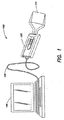
図1は、センサアレイ110、ハンドルインタフェース120、計算装置140、及び計算装置とハンドルインタフェースとの間の通信リンク130を含むセンサシステム100の一実施形態を示す。典型的なセンサアレイ110は、圧力又は力の変化に応答して抵抗を変化させる抵抗素子を含むことができるが、容量センサを含むがこれに制限されない他の種類のセンサも可能である。センサアレイは行/列フォーマットに構成することができるが、他の構成も可能であり、本発明はこの点で制限されない。例えば、典型的なセンサは、52個の駆動電極及び44個の受信電極のアレイで形成することができ、駆動電極と受信電極との各交点がセンサ素子に対応することができる。本明細書において使用するセンサ素子は、任意の適したサイズ及び/又は形状を有することができ、本発明はこの点で制限されない。一実施形態では、センサ素子は、駆動電極と受信電極との交点によって形成することができるセンサ点であることができる。
FIG. 1 illustrates one embodiment of a
ハンドルインタフェース120は、センサアレイ110に結合することができる回路であって、センサ素子の走査、センサ素子ばらつきの補償、及び/又は感度調整を制御することができる回路を含むことができる。ハンドルインタフェース120と計算装置140との間の通信リンク130は、有線又は無線通信リンクを含めた任意の適した種類の通信パスを含むことができる。有線通信リンクのいくつかの種類としては、パラレルインタフェース、USBインタフェース、及びPCIインタフェースを挙げることができるがこれらに制限されない。無線通信リンクのいくつかの種類としては、ブルートゥース(Bluetooth)及び802.11無線インタフェースを挙げることができるがこれらに制限されない。計算装置140は、ユーザが走査されたセンサ素子に対応する圧力データ又は力データを見られるようにし、且つ/又はハンドルインタフェース120の動作を制御できるようにする装置を含むことができるがこれらに制限されない。計算装置140は、パーソナルコンピュータ、個人情報端末、及び/又はサーバを含むことができるがこれらに制限されない。計算装置140は、収集されたセンサデータの表示、解析、及び/又は記憶並びに/或いはハンドルインタフェース120の制御を可能にするソフトウェアを含むことができる。
The
ハンドルインタフェースは、走査制御及び計算装置へのインタフェースとして機能することができるため、ハンドルインタフェースの性能は、センサシステムの全体性能、ロバスト性、及び柔軟性を決める際の要因であり得る。従来のインタフェースは、センサ素子毎に約50μsのレートでセンサデータを取得するデータ取得電子回路を含むことができる。典型的なアレイは約52×44=2288個のセンサ素子で形成することができるため、センサ素子サンプリングレートが50μsの場合、100msを越える合計アレイ(又はフレーム)データ取得時間になり、ひいては毎秒で合計約10フレームが取得されることになる。これは、2288個の各センサ素子が毎秒約10回取得され、すなわち毎秒で合計約2288×8=18304回のセンサ素子取得を暗示する。取得された各センサ素子電圧は、アナログ/デジタル変換を受けることができ、したがって、取得レートは毎秒で取得されるデジタルビット数(又はバイト数)で表すことができる。8ビットアナログ/デジタル変換器(ADC)の場合、従来のインタフェースの取得データレートは、約18304×8ビット/s=18.3キロバイト/s、すなわち約0.15メガビット/sで与えることができる。 Since the handle interface can function as an interface to the scan control and computing device, the performance of the handle interface can be a factor in determining the overall performance, robustness, and flexibility of the sensor system. A conventional interface can include data acquisition electronics that acquire sensor data at a rate of about 50 μs per sensor element. Since a typical array can be formed with about 52 × 44 = 2288 sensor elements, a sensor element sampling rate of 50 μs results in a total array (or frame) data acquisition time of over 100 ms, and hence every second A total of about 10 frames will be acquired. This implies that 2288 sensor elements are acquired approximately 10 times per second, ie a total of approximately 2288 × 8 = 18304 sensor element acquisitions per second. Each acquired sensor element voltage can be subjected to analog / digital conversion, and thus the acquisition rate can be expressed in digital bits (or bytes) acquired per second. For an 8-bit analog to digital converter (ADC), the acquisition data rate of the conventional interface can be provided at about 18304 × 8 bits / s = 18.3 kilobytes / s, ie about 0.15 megabits / s. .
このような従来のシステムでは、センサデータを計算装置インタフェースに転送する前、圧力情報又は力情報を測定するメカニズム、データをデジタルフォーマットに変換するメカニズム、及びデジタルデータを通信インタフェースに転送するメカニズムが制限要因であり得る。例えば、USB1.1通信リンクは、データを通信装置に最大レート12メガビット/sで転送することができるが、実際には、典型的なレートは、オーバーヘッド制限により約9メガビット/sである。したがって、データがハンドルインタフェースによって提供される場合、データを計算装置に約9Mビット/sのレートで転送することができる。しかし、ハンドルインタフェースがデータを転送に提供するレートは、上述した従来の0.15メガビット/データ取得レートで示したように、通信リンクの達成可能なデータ転送速度よりもかなり低いことがある。 Such conventional systems have limited mechanisms for measuring pressure or force information, converting data to digital format, and transferring digital data to the communication interface before transferring sensor data to the computing device interface. It can be a factor. For example, a USB 1.1 communication link can transfer data to a communication device at a maximum rate of 12 megabit / s, but in practice a typical rate is about 9 megabit / s due to overhead limitations. Thus, if the data is provided by the handle interface, the data can be transferred to the computing device at a rate of about 9 Mbit / s. However, the rate at which the handle interface provides data for transfer may be significantly lower than the achievable data transfer rate of the communication link, as indicated by the conventional 0.15 megabit / data acquisition rate described above.
本明細書に提示されるいくつかの実施形態では、センサアレイを計算装置に結合し、従来のハンドルインタフェースと比較して高速のレートでデータを通信リンクバッファに転送するハンドルインタフェースが提供される。ハンドルインタフェースは、従来のハンドルインタフェースのデータ転送レートよりも約1桁(例えば、約2桁)大きなレートでデータを出力することができる。一実施形態では、ハンドルインタフェースは、データを取得し、約3メガビット/sのレートで通信リンクバッファ(例えば、USBバッファ)に送信することができる。いくつかの実施形態では、このようなレートは、パラレルモジュールを含む制御回路を実施することによって達成することができる。一実施形態では、制御回路はフィールドプログラマブルゲートアレイ(FPGA)を含む。FPGAアーキテクチャの並列性は、可変レジスタ長を構成する能力及びより高速なクロックレートと共に、データ取得レートをUSB最大転送レートに近づけられるようにすることができる。FPGA制御回路は、ハンドル内の高速ADC及び高帯域幅演算増幅器を制御して、データ取得レートをさらに増大させることができる。いくつかの実施形態では、ハンドルインタフェースは、リアルタイムでの圧力又は力のマッピングを可能にするような大型センサアレイのデータ取得レート及び転送レートを可能にすることができる。一実施形態では、ハンドルインタフェースは、約2288個のセンサ素子が毎秒約100回サンプリングできるようにし、一実施形態では、最大で毎秒約500回サンプリングできるようにする。 In some embodiments presented herein, a handle interface is provided that couples a sensor array to a computing device and transfers data to a communication link buffer at a higher rate compared to a conventional handle interface. The handle interface can output data at a rate approximately one digit (eg, approximately two digits) greater than the data transfer rate of the conventional handle interface. In one embodiment, the handle interface can acquire and send data to a communication link buffer (eg, USB buffer) at a rate of about 3 megabits / s. In some embodiments, such a rate can be achieved by implementing a control circuit that includes a parallel module. In one embodiment, the control circuit includes a field programmable gate array (FPGA). The parallelism of the FPGA architecture can allow the data acquisition rate to approach the USB maximum transfer rate, along with the ability to configure variable register lengths and faster clock rates. The FPGA control circuit can control the high speed ADC and high bandwidth operational amplifier in the handle to further increase the data acquisition rate. In some embodiments, the handle interface may allow for data acquisition and transfer rates for large sensor arrays that allow real-time pressure or force mapping. In one embodiment, the handle interface allows about 2288 sensor elements to sample about 100 times per second, and in one embodiment allows up to about 500 times per second to sample.
本明細書に提示される各種実施形態では、センサアレイを計算装置に結合するハンドルインタフェースであって、センサアレイ全体の1つ又は複数のサブセットに属するユーザ定義可能なセンサ素子の走査を可能にするハンドルインタフェースが提供される。いくつかのこのような実施形態では、ユーザは、センサアレイ全体のセンサ素子の1つ又は複数のサブセット、例えば1個のセンサ素子、いくつかのセンサ素子、いくつかの行、いくつかの列、及び/又は行及び列のうちのいくつかを定義することができる。いくつかの実施形態では、ユーザは、計算装置に表示されるセンサアレイの視覚表現において1つ又は複数の形状を指定することにより、センサ素子の1つ又は複数のサブセットを定義することができる。センサアレイ全体の1つ又は複数のサブセットが定義されると、ハンドルインタフェースが収集して転送する必要があるのは、定義された1つ又は複数のサブセットに属するセンサ素子からのデータのみであり、それにより、フレームサンプリングレートを高速化することが可能である。したがって、本明細書に提示されるいくつかのハンドルインタフェースは、ユーザが、より大きな圧力マップ又は力マップの定義可能な1つ又は複数のサブセットにフォーカスでき、オプションとして、定義可能な1つ又は複数のサブセットのデータをより高速のフレームサンプリングレートで収集できるようにすることができる。 In various embodiments presented herein, a handle interface that couples a sensor array to a computing device that allows scanning of user-definable sensor elements that belong to one or more subsets of the entire sensor array A handle interface is provided. In some such embodiments, the user can use one or more subsets of sensor elements of the entire sensor array, such as one sensor element, several sensor elements, several rows, several columns, And / or some of the rows and columns can be defined. In some embodiments, the user can define one or more subsets of sensor elements by specifying one or more shapes in the visual representation of the sensor array displayed on the computing device. When one or more subsets of the entire sensor array are defined, the handle interface only needs to collect and transfer data from sensor elements belonging to the defined one or more subsets, As a result, the frame sampling rate can be increased. Accordingly, some handle interfaces presented herein allow the user to focus on one or more definable subsets of a larger pressure map or force map, and optionally one or more definable ones. Can be collected at a faster frame sampling rate.
本明細書に提示される各種実施形態では、センサ素子のばらつきによる収集データの相違を考慮することができるセンサアレイ較正方法が提供される。本明細書に提示されるいくつかの実施形態では、利得調整方法も提供される。 In various embodiments presented herein, a sensor array calibration method is provided that can account for differences in collected data due to variations in sensor elements. In some embodiments presented herein, a gain adjustment method is also provided.
図2は、センサアレイが、ハンドルインタフェース内に存在することができる回路に結合される一実施形態を示す。センサ行列アレイ10は、複数の第1の又は入力(すなわち、駆動)電極12−1〜12−4及び複数の第2の又は出力(すなわち、感知又は受信)電極14−1〜14−4から形成される。これら電極は、Mylar又は別の基板材料等のプラスチック材料の薄い基板上に形成することができ、基板は、圧力又は力感応インク或いは他の圧力又は力感応材料の層によって隔てられる。圧力又は力感応材料(例えば、インク)は、圧力又は力感応可変抵抗材料及び/又は可変容量材料を含むことができる。
FIG. 2 illustrates one embodiment in which the sensor array is coupled to circuitry that can be present in the handle interface. The
第1の各電極と第2の各電極との交点が、センサ素子P1〜P16を形成する。各センサ素子は、センサ素子に印加される圧力又は力に伴って変化する抵抗R1〜R16であって、圧力又は力が素子に印加されていないときにはメガオームのオーダで非常に大きく、圧力又は力が素子に印加されているときにはわずか1000オームである抵抗R1〜R16を有する。特に回路内に設計されないが、各センサ素子にはトレースコンデンサC1〜C16もあってよく、静電容量は3〜8ピコファラデーのオーダであり得る。コンデンサは、間に誘電体として機能する薄い可変抵抗層を有する電極をプレートとして形成される。16個のセンサ素子のみが図1の実施形態に示されるが、任意の数のセンサ素子を利用してよく、本発明はこの点に制限されないことを理解されたい。 Intersections between the first electrodes and the second electrodes form sensor elements P1 to P16. Each sensor element is a resistor R1-R16 that varies with the pressure or force applied to the sensor element, and is very large on the order of mega ohms when no pressure or force is applied to the element. It has resistors R1-R16 that are only 1000 ohms when applied to the device. Although not specifically designed in the circuit, each sensor element may also have trace capacitors C1-C16, and the capacitance may be on the order of 3-8 picofaraday. The capacitor is formed as an electrode having a thin variable resistance layer functioning as a dielectric in between. Although only 16 sensor elements are shown in the embodiment of FIG. 1, it should be understood that any number of sensor elements may be utilized and the invention is not limited in this respect.
線18上の駆動信号又は電圧Vdriveが、第1のマルチプレクサ又はスイッチ16を通して第1の各電極12に印加される。各電極12−1〜12−4は、図2中で、駆動電圧が通る一塊の抵抗R23、R24、R25、及びR26で示される固有トレース抵抗を有する。接地へのパラレルパスも、ブリードオフ(bleed-off)抵抗R27、R28、R29、及びR30のそれぞれを通して各入力電極12に提供することができ、これらブリードオフ抵抗を通して、センサ素子のトレース静電容量を素早く放電することができ、それにより、センサ素子の走査の合間での回路の整定時間がわずか1μ秒に短縮される。これら各抵抗の値は比較的低くてよく、例えば、2〜10kΩの範囲内であることができる。
A drive signal or voltage Vdrive on
一実施形態では、駆動電圧(Vdrive)は、マルチプレクサ16の各スイッチS1〜S4に印加され、各スイッチは対応する固有の抵抗を有し、図中、これは一塊の抵抗R36、R37、R38、及びR39としてそれぞれ示される。これら抵抗は通常、50〜100Ωの範囲内である。Vdrive線18上の信号は、抵抗R31を通して演算増幅器20から得られる。R31の増幅器20に隣接する側の電圧は、抵抗R32を通して演算増幅器22の負入力に接続されるとともに、抵抗R34を通してA/D変換器24の電圧入力にも接続される。抵抗R31の他方の側の電圧は、R21を通してフィードバックとして演算増幅器20に印加され、抵抗R21を通る信号は、抵抗R22を通って接地にも接続される。さらに、抵抗R31の他方の側の信号は、抵抗R33を通って演算増幅器22の正入力に印加されるとともに、抵抗R35を通して接地に接続される。
In one embodiment, a drive voltage (Vdrive) is applied to each switch S1-S4 of
図2に示す実施形態では、Vdrive線18上の抵抗R31を通過する負荷電流を示す演算増幅器22からの出力は、A/D変換器24のVin入力に接続される。変換器24への他方の入力は、変換器電圧基準入力であり、線28を介して固定電圧源26から得られる。線28上の信号は、D/A変換器30及び32の基準入力にも印加される。変換器30及び32へのデジタル入力は、制御回路34から線35上で得られる。
In the embodiment shown in FIG. 2, the output from the
いくつかの実施形態では、制御回路34は、フィールドプログラマブルゲートアレイ(FPGA)を含むことができ、FPGAは、本明細書において述べる各種機能のうちの1つ又は複数を実行することができるプログラマブル論理構成要素及びプログラマブル相互接続を含む。他の実施形態では、制御回路34は、各種機能を実行するようにプログラムされる標準マイクロプロセッサ又は他のプロセッサを含むことができる。いくつかの実施形態では、制御回路34は、これら機能を実行する専用ハードウェア、機能自体のうちのいくつかを実行し、その他の機能を実行する他の処理回路とのインタフェースとして機能する何らかの種類のハイブリッド回路、又は他の適した制御回路であってよい。各種実施形態での制御回路34の特徴をさらに以下において述べる。
In some embodiments, the
変換器30は、線36上に基準電圧を生成し、この基準電圧は出力A/D変換器38の基準入力に印加され、D/A変換器32への入力は駆動電圧を示す。D/A変換器32から出力される駆動電圧は、線40を通して演算増幅器20の正入力に印加される。線40上の電圧は、増幅器20を通過せずにそのままVdriveとして使用することができるが、R31による電圧降下を補償するための増幅器20及び関連回路を含むことが好ましいであろう。A/D変換器38のVin入力は、出力マルチプレクサ44から線42に出力される。
出力マルチプレクサ44は、受信マルチプレクサとも呼ばれ、演算増幅器46−1〜46−4の出力から各入力を受け取る。各演算増幅器は、対応する電極14−1〜14−4の信号を負入力で受け取る。抵抗R40、R41、R42、R43は、対応する出力電極のトレース抵抗を表す。各演算増幅器の出力は、対応する抵抗R18、R19、R20、及びR21を通してそれぞれフィードバックもされる。各演算増幅器46への正入力は接地に接続される。各演算増幅器46のフィードバック信号の効果は、対応する電極の出力端を実質的に接地電位に保つことである。増幅器46の出力は、電極14の信号/電流を反映する。
The
マルチプレクサ44からの出力線42は、比較器48の正入力にも接続される。比較器48への負入力は、線50上の閾値電圧である。したがって、比較器48は、アレイ10で検出される信号がある所定の閾値を超える場合のみ回路34を制御する出力を線52上に生成する。変換器38からのデジタル出力は制御回路34に接続され、制御回路34は、変換器38から受信した出力を処理し、出力信号をデジタル出力線54上に生成する。
The
デジタル出力線54上の出力は、USBインタフェース等の有線インタフェース又はブルートゥース(Bluetooth)若しくは802.11インタフェース等の無線インタフェースを含むがこれらに制限されない任意の適したインタフェースを介して計算装置(図示せず)に結合することができる。計算装置(図示せず)から制御回路34への通信は、デジタル出力線54について説明したインタフェース等の任意の適したインタフェースを介してデジタル入力線55を経由して達成することができる。
The output on the
図2の回路は、本願と同一の譲受人に譲渡された米国特許第5,505,072号明細書(第‘072号明細書)及び米国特許第4,856,993号明細書(第‘993号明細書)に提示される回路と同様であり、これら両特許を参照により本明細書に援用する。動作に際して、図2の回路は、第‘072号明細書及び第‘993号明細書に提示される走査動作と同様にしてセンサアレイの走査を実行することができ、第‘072号明細書及び/又は第‘993号明細書の回路の特徴のうちのいくつかを組み込むことができる。さらに、又はあるいは、図2の回路及び本明細書に提示される他の実施形態は、以下においてさらに述べる制御回路特徴を組み込むことができる。 The circuit of FIG. 2 is shown in U.S. Pat. No. 5,505,072 ('072) and U.S. Pat. No. 4,856,993 (No.') assigned to the same assignee as the present application. 993)), both of which are incorporated herein by reference. In operation, the circuit of FIG. 2 can perform a scan of the sensor array in a manner similar to the scanning operations presented in the '072 and' 993 specifications. Some of the features of the '993 circuit may be incorporated. Additionally or alternatively, the circuit of FIG. 2 and other embodiments presented herein may incorporate control circuit features that are further described below.
本明細書に提示される制御回路特徴が、センサアレイの走査を制御し、且つ/又はセンサアレイからデータを収集する他の回路構成に組み込むことも可能であり、本発明が本明細書に提示される実施形態に制限されないことを理解されたい。例えば、制御回路に結合されたセンサアレイを含むセンサシステムの代替の実施形態が、本願と同一の譲受人に譲渡された米国特許第5,905,209号明細書(第‘209号明細書)に提示されており、これを参照により本明細書に援用する。 The control circuit features presented herein can be incorporated into other circuitry that controls scanning of the sensor array and / or collects data from the sensor array, and the present invention is presented herein. It should be understood that the present invention is not limited to the embodiments described. For example, an alternative embodiment of a sensor system including a sensor array coupled to a control circuit is disclosed in US Pat. No. 5,905,209 ('209) assigned to the same assignee as the present application. Which is hereby incorporated by reference.
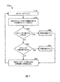
上述したように、いくつかの実施形態では、ユーザは、センサアレイのセンサ素子の1つ又は複数のサブセットを定義することができる。センサアレイの走査中、センサ素子の1つ又は複数のサブセットを走査する必要がある。図3aは、流れ図300aで示される、センサアレイのセンサ素子の1つ又は複数のサブセットを定義できるようにする方法の実施形態である。ステップ310において、ユーザがセンサアレイの1つ又は複数のサブセットを定義することができるようなユーザインタフェースを提供することができる。ユーザインタフェースは、図1のセンサシステムに示すように、センサアレイのハンドルインタフェースに結合される計算装置に提示することができる。ユーザインタフェースは、センサアレイの視覚表現を含むことができ、ユーザが、個々のセンサ素子を選択することにより且つ/又は他の任意の手段により、図4に示すようなセンサアレイ表現内の1つ又は複数の所望の形状及び/又は境界を定義することで、センサ素子の1つ又は複数のサブセットを定義できるようにすることができ、本発明はこの点で制限されない。
As described above, in some embodiments, a user can define one or more subsets of sensor elements of a sensor array. During scanning of the sensor array, one or more subsets of sensor elements need to be scanned. FIG. 3a is an embodiment of a method that allows one or more subsets of sensor elements of a sensor array to be defined as shown in
表現400において、センサアレイ410のセンサ素子は、駆動電極412と受信電極414との交点にある。説明のために、矩形センサアレイ410が提示されるが、他の任意のセンサアレイ構成も可能なことを理解されたい。表現400において、ユーザは、データを収集すべきセンサ素子の1つ又は複数のサブセットを囲む境界を定義するように、矩形440、円又は楕円430、及び/又は不規則形450を含む各種形状及び/又は境界を定義する(例えば、ポインタを使用して描画することを介して)ことができる。さらに、又はあるいは、センサ素子460及び470に示すように1つ又は複数のセンサ素子を選択することにより、1つ又は複数の行を選択することにより(図示せず)、且つ/又は1つ又は複数の列を選択することにより(図示せず)センサ素子の1つ又は複数のサブセットを定義することを含むがこれらに制限されない、走査データを収集すべきセンサ素子のサブセットを定義する他の方法を使用してもよい。
In
さらに、又はあるいは、センサ素子の1つ又は複数のサブセットは、センサアレイ表現に重ねられるパターンによって定義してもよい。例えば、センサアレイ表現に重ねられた矩形チェッカーボードパターンにより、パターンが塗りつぶされた領域(例えば、チェッカーボードパターンの塗りつぶされた矩形)内のセンサ素子の1つ又は複数のサブセットを定義することができる。このようなパターンは、パターンの塗りつぶされた領域のサイズに基づいて、走査されるセンサ素子の空間分解能を指定できるようにする。例えば、特定の空間分解能を有する圧力データ又は力データが望まれ、センサアレイが所望の空間分解能よりも高いセンサ素子を含む場合、パターン(例えば、チェッカーボードパターン)を使用して、走査するセンサ素子のサブセットを定義することができる。このようにすれば、収集する必要があるのは、所望の分解能をもたらし、且つ/又はセンサアレイの所望の領域にフォーカスされたセンサ素子のデータのみである。さらに、センサ素子の1つ又は複数のサブセットの定義は必ずしもグラフィックス的に実行される必要はなく、1つ又は複数のサブセットの座標入力等の他の方法を使用してもよいことを理解されたい。 Additionally or alternatively, one or more subsets of sensor elements may be defined by a pattern superimposed on the sensor array representation. For example, a rectangular checkerboard pattern overlaid on the sensor array representation can define one or more subsets of sensor elements within the area where the pattern is filled (eg, a filled rectangle of the checkerboard pattern). . Such a pattern allows the spatial resolution of the scanned sensor elements to be specified based on the size of the filled area of the pattern. For example, if pressure or force data having a particular spatial resolution is desired and the sensor array includes sensor elements that are higher than the desired spatial resolution, the sensor elements that are scanned using a pattern (eg, a checkerboard pattern) A subset of can be defined. In this way, it is only necessary to collect data for sensor elements that provide the desired resolution and / or are focused on the desired area of the sensor array. Further, it will be appreciated that the definition of one or more subsets of sensor elements need not necessarily be performed graphically, but other methods such as coordinate input of one or more subsets may be used. I want.
ステップ320において、ユーザインタフェースを提示している計算装置は、センサ素子の定義された1つ又は複数のサブセットを受け取ることができる。ステップ330において、センサ素子の定義された1つ又は複数のサブセットを使用して、センサアレイのセンサ素子の1つ又は複数のサブセット内にあるセンサ素子を示す走査テーブルを生成することができる。走査テーブルは、定義された1つ又は複数のサブセット内の任意の適したセンサ素子表現を含むことができる。いくつかの実施形態では、センサ素子は、各駆動線の1つ又は複数の駆動線及び1つ又は複数の受信線を参照することによって特定することができ、それにより、センサ素子の1つ又は複数のサブセットの二次元座標表現を提供することができる。
In
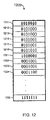
例えば、図12に示すように、走査テーブル1200は、7ビット値のリストを含むことができ、各値の最初のビットは、新しい駆動線を示すために使用することができる。走査テーブル1200内で、最初のビット「1」は新しい駆動線を示し、その他の6ビットは、参照される特定の駆動線を定義する。逆に、最初のビット値「0」は、最も新しく参照された駆動線上の特定のセンサ素子を示し、その他の6ビットは、参照されている特定の受信線を特定する。例えば、テーブル内の値1211は最初のビット「1」を有し、新しい駆動線がこの値によって特定されることを暗示し、駆動線は続く6ビット「010010」によって定義される。次の値1212は、値1211によって定義される最も新しく参照された駆動線上の特定のセンサ素子を示す。同様に、値1213〜1216はすべて、最初のビット「0」を有し、値1211によって与えられる最も新しく参照された駆動線と交わる受信線の特定を介して特定のセンサ素子を示す。値1221は、最初のビット「1」を有し、新しい駆動線が値の続く6ビットによって特定されることを示す。値1222〜1224は、値1221によって与えられる最も新しく参照された駆動線と交わる受信線の特定を介して特定のセンサ素子を定義する。
For example, as shown in FIG. 12, scan table 1200 can include a list of 7-bit values, and the first bit of each value can be used to indicate a new drive line. Within scan table 1200, the first bit “1” indicates a new drive line, and the other 6 bits define the particular drive line referenced. Conversely, the first bit value “0” indicates the specific sensor element on the most recently referenced drive line, and the other 6 bits specify the specific receive line being referenced. For example, the
走査テーブル1200は、センサアレイ全体の1つ又は複数のサブセット内の各センサ素子の駆動線及び対応する受信線を特定する任意の数のこのような7ビット値を有することができる。走査テーブル1200内で、7ビット値「1111111」(値1720)はテーブルの終わりを示すが、テーブルの終わりを示すために他の任意の値を使用してよいことを理解されたい。これは走査テーブルの単なる一例にすぎず、値の変更が可能なことを理解されたい。例えば、一変更は、テーブルの値に任意の所望の数のビット(例えば、6ビット、7ビット、8ビット、9ビット等)を使用することを含むことができ、テーブルの値は必ずしも上述した例示的な7ビット実施形態に制限されない。走査テーブルの値の所望のビット数は、センサアレイのセンサ素子を一意に識別するように、センサアレイの駆動線数及び受信線数に基づいて選択することができる。 The scan table 1200 may have any number of such 7-bit values that identify the drive line and corresponding receive line for each sensor element in one or more subsets of the entire sensor array. Within scan table 1200, the 7-bit value “1111111” (value 1720) indicates the end of the table, but it should be understood that any other value may be used to indicate the end of the table. It should be understood that this is just one example of a scan table and that values can be changed. For example, one change can include using any desired number of bits (eg, 6 bits, 7 bits, 8 bits, 9 bits, etc.) in the table values, and the table values are not necessarily described above. It is not limited to the exemplary 7-bit embodiment. The desired number of bits of the scan table value can be selected based on the number of drive lines and the number of receive lines of the sensor array so as to uniquely identify the sensor elements of the sensor array.
図3aに戻り、走査テーブル330が生成されると、定義された走査エリアに対応する走査テーブルを走査に使用することができ、且つ/又はステップ340に示すように、(例えば、計算装置の)記憶装置に保存することができる。将来に使用するために、ユーザが望む任意の数のこのような走査テーブルを保存することができる。 Returning to FIG. 3a, once the scan table 330 has been generated, the scan table corresponding to the defined scan area can be used for the scan and / or as shown in step 340 (eg, of the computing device). It can be stored in a storage device. Any number of such scan tables desired by the user can be stored for future use.
図3bは、流れ図300bで示される、所望の走査テーブルを使用してセンサアレイを走査する方法の一実施形態である。ステップ350において、センサアレイの定義された1つ又は複数のサブセットに対応する所望の走査テーブルが、通信リンクを介して計算装置からハンドルインタフェースに転送される。ハンドルインタフェースは、通信リンクを介して走査テーブルを受信することができ(ステップ360)、走査テーブルをハンドルの走査テーブルメモリに記憶することができる(ステップ370)。いくつかの実施形態では、ステップ360及び370は、ハンドルインタフェース内の制御回路によって実行することができ、走査テーブルメモリは制御回路内に備えることができる。例示的な実施形態では、走査テーブルメモリは、FPGA制御回路内のレジスタを含むことができる。センサアレイの走査中、ハンドルインタフェースは、走査テーブルメモリ内の走査テーブルを使用して、データを収集して計算装置に転送すべきセンサ素子を選択することができる。
FIG. 3b is one embodiment of a method for scanning a sensor array using a desired scan table, shown in
いくつかの実施形態では、センサアレイのセンサ素子は、センサアレイのセンサ素子間のパス抵抗のばらつきを考慮するように較正することができる。センサ素子間のパス抵抗のばらつきは、(例えば、異なるセンサ素子の異なる電極長による)センサ素子間の駆動電極及び受信電極のトレース抵抗のばらつき、(例えば、交わる電極の間隔及び/又は電極間の材料の抵抗のばらつきによる)センサ素子抵抗のばらつき、及び/又はセンサ素子間の他の任意の抵抗ばらつきにより得る。図5は、流れ図500によって示される、センサアレイのセンサ素子の較正を可能にする方法の実施形態である。 In some embodiments, the sensor elements of the sensor array can be calibrated to account for variations in path resistance between the sensor elements of the sensor array. Variations in path resistance between sensor elements may include variations in trace resistance of drive and receiver electrodes between sensor elements (eg, due to different electrode lengths of different sensor elements), eg, spacing between intersecting electrodes and / or between electrodes Obtained by variations in sensor element resistance (due to variations in material resistance) and / or any other resistance variation between sensor elements. FIG. 5 is an embodiment of a method that allows calibration of sensor elements of a sensor array, illustrated by flow diagram 500.
このような較正は、センサアレイのセンサ素子間のパス抵抗のあらゆるばらつきの補償に使用することができる。このような較正は、大型センサアレイの場合に特に有用であることができ、大型センサアレイでは、長い電極の大きな電圧降下により、センサ素子間のパス抵抗のばらつきを補償するように各センサ素子に印加される駆動電圧を変更することが非常に有益であり得る。走査中、このような補償は、ハンドル内の回路により、例えば所与のセンサ素子が走査に選択されたときに駆動電流を測定し、それに従って駆動電圧(又は基準電圧)を補償することによって実行することができる。駆動電圧は、選択されたセンサ素子の駆動電流にパス抵抗を乗算したものに基づいて補償することができ、選択されたセンサ素子のパス抵抗は、前のセンサアレイ較正手順中に求めることができる。 Such calibration can be used to compensate for any variation in path resistance between the sensor elements of the sensor array. Such calibration can be particularly useful in the case of large sensor arrays, where the large voltage drop across the long electrodes causes each sensor element to compensate for variations in path resistance between sensor elements. It can be very beneficial to change the applied drive voltage. During scanning, such compensation is performed by circuitry within the handle, for example by measuring the drive current when a given sensor element is selected for scanning and compensating the drive voltage (or reference voltage) accordingly. can do. The drive voltage can be compensated based on the drive current of the selected sensor element multiplied by the path resistance, and the path resistance of the selected sensor element can be determined during a previous sensor array calibration procedure. .
一実施形態では、センサアレイ較正プロセス500は、センサアレイがハンドルに結合されるときに実行することができる。センサアレイ較正手順は、ハンドル内の制御回路によって実行することができる。センサアレイ較正は、センサアレイ内のセンサ素子に圧力又は力を印加して、センサアレイのすべてのセンサ素子にわたる受信線A/D変換器の平均所望出力を得ること(ステップ510)を含むことができる。印加される圧力又は力は、センサアレイ全体にわたって実質的に均等な圧力又は力であることができる。例えば、センサアレイをブラダー内に配置し、センサ素子毎の平均所望受信線A/D出力を生成するのに十分な圧力又は力を印加することができる。例えば、平均所望受信線A/D出力は、8ビットA/D変換器の場合、最大読み取り値255のうち、センサ素子毎に約190であることができる。センサ素子にわたる受信線A/D変換器の所望の出力を得ることが、他の適した手法を使用して達成することもでき、必ずしも圧力又は力をセンサ素子に印加することを介して達成する必要がないことも理解されたい。
In one embodiment, the sensor
各センサ素子について(ステップ520)、ハンドルの駆動電圧をデフォルト値に設定することができる(ステップ530)。例えば、デフォルト値は約0.3Vにすることができる。選択されたセンサ素子の仮定パス抵抗もデフォルト値に設定することができる(ステップ540)。例えば、大型センサアレイの場合、デフォルト値は128Ωにすることができる。 For each sensor element (step 520), the handle drive voltage can be set to a default value (step 530). For example, the default value can be about 0.3V. The assumed path resistance of the selected sensor element can also be set to a default value (step 540). For example, for a large sensor array, the default value can be 128Ω.
選択されたセンサ素子の受信線A/D変換器出力が所望のレベル、例えば、上述したように190の読み取り値であるか否かがを判断することができる(ステップ550)。これが当てはまる場合、方法はステップ590に進み、選択されたセンサ素子の仮定パス抵抗が記憶される。これが当てはまらない場合、方法は受信線A/Dからの出力が所望のレベルに達するまで、駆動電圧を変化させることに進むことができる。方法500では、このようなプロセスは、駆動電流を読み取ること(ステップ560)、例えば仮定パス抵抗を増分的に増大させ、且つ/又は低減することによって仮定パス抵抗を変化させること(ステップ570)、及び駆動電流に仮定パス抵抗とデフォルトパス抵抗との差を乗算したものを加算することによって駆動電圧を変更すること(ステップ580)を含むことができる。プロセスはステップ550に続き、受信線A/Dが選択されたセンサ素子について所望のレベルを達成したか否かが再び判断される。
It can be determined whether the receive line A / D converter output of the selected sensor element is at a desired level, eg, 190 readings as described above (step 550). If this is the case, the method proceeds to step 590 where the assumed path resistance of the selected sensor element is stored. If this is not the case, the method can proceed to changing the drive voltage until the output from the receive line A / D reaches the desired level. In
プロセスは、ステップ550におけるテストにより、所望のレベルに達したと判断されるまで繰り返され、次に、ステップ530〜590がセンサアレイの各センサ素子について繰り返される。プロセス500が完了すると、センサアレイの各センサ素子についてのパス抵抗を含むことができるセンサアレイ較正ファイルを生成することができる。同じ種類の特定のセンサアレイがセンサアレイ間の許容差のばらつきによりわずかに異なる較正ファイルを有し得ることを理解されたい。センサアレイ較正ファイルは、ハンドルから結合された計算装置に転送し、特定のセンサアレイに対応する識別番号と共に記憶することができる。図示のプロセスを介して生成されるパス抵抗が、必ずしも各センサ素子の実際のパス抵抗に対応する必要はなく、むしろパス抵抗間の相対差を示すことも理解されたい。したがって、本明細書において使用されるセンサ素子のパス抵抗は、パス抵抗間の相対差を示す値の包含も意味する。
The process is repeated until the test in
図6は、流れ図600で示される、対応するセンサアレイの走査動作中にセンサアレイ較正データ(図5の方法によって生成される較正データ等)を使用する方法の実施形態である。このようなプロセスは、ハンドル内の制御回路(例えば、制御回路34)によって実行することができる。走査中、選択された各センサ要素について(ステップ610)、駆動電流がハンドル内で読み取られる(ステップ620)。例えば、駆動電流は、図2のA/D変換器24の出力に基づいて測定することができる。次に、選択されたセンサ素子の記憶されているパス抵抗較正データを検索して、センサアレイのセンサ素子間のばらつきを考慮した駆動電圧補償を可能にすることができる。特に、選択されたセンサ素子のパス抵抗を検索することができる(例えば、制御回路34内のレジスタ内から)(ステップ630)。選択されたセンサ素子のパス抵抗及び駆動電流読み取り値に基づいて、選択されたセンサ素子のパス抵抗による電圧降下の計算を、例えば、オームの法則を使用して、すなわち電流をパス抵抗で乗算することによって実行することができる(ステップ640)。駆動電圧は、計算された電圧降下を駆動電圧に加算することによって補償することができる(ステップ650)。このようなプロセスは、選択された各センサ素子に対して実行することができ、それにより、センサアレイのセンサ素子間のパス抵抗ばらつきを補償することができる。上述したように、このような補償プロセスは、長い電極を有する大型センサアレイの場合に非常に有利であり得る。
FIG. 6 is an embodiment of a method for using sensor array calibration data (such as calibration data generated by the method of FIG. 5) during the scanning operation of the corresponding sensor array shown in
各種実施形態では、センサアレイのセンサ素子からの受信信号に適用される利得は、自動的に補償することができる。いくつかの実施形態では、利得の調整は、収集されたセンサデータの各フレームに対して実行することができる。図7は、流れ図700で示される、ハンドル内で実行することができる自動利得補償方法の実施形態である。一実施形態では、ハンドル内の制御回路は、前のフレームからの受信値に基づいてあらゆるフレームの受信線A/D変換器の利得を調整することができる。各フレームについて(710)、閾値を超える受信線A/D変換器出力の数のカウントを求めることができる(ステップ720)。8ビットA/D変換器の場合、閾値の一例は220であることができる。カウントは、フレーム全体の信号強度を示すものとして機能することができる。走査されるすべてのセンサ素子の総合信号値又は平均信号値を含むがこれに制限されない他の種類の信号強度値を使用してもよいことを理解されたい。カウント、より一般には走査フレームにわたる信号強度を測るために使用される任意の信号強度値は、制御回路内のレジスタ内に記憶することができる。
In various embodiments, the gain applied to the received signal from the sensor elements of the sensor array can be automatically compensated. In some embodiments, gain adjustment may be performed for each frame of collected sensor data. FIG. 7 is an embodiment of an automatic gain compensation method shown in
フレームの終わりに、カウントが上限よりも大きいか否かを判断することができる(ステップ730)。例えば、上限値は、走査されるセンサ素子総数の10%であることができる。カウントが上限よりも大きい場合、受信線A/D変換器の利得を低減することができる(ステップ740)。受信線A/D変換器の利得は、基準電圧及び/又は駆動電圧を変化させることによって低減することができる。カウントが上限以下である場合、カウントが下限未満であるか否かを判断することができる(ステップ750)。下限未満の場合、受信線A/D変換器の利得を増大することができる(ステップ760)。下限未満ではない場合、プロセスは、受信線A/D変換器の利得を変化させることなく続けられる。受信線A/D変換器の利得値は、所与のフレームに適用される利得に基づいて各フレームの受信走査データを適宜正規化できるように、走査センサデータを受け取る計算装置に送信することができる(ステップ770)。閾値、カウント上限、及び/又はカウント下限が、ユーザにより設定されてもよく、デフォルト値をとってもよく、且つ/又は他の任意の適した手段を介して設定されてもよいことを理解されたい。 At the end of the frame, it can be determined whether the count is greater than the upper limit (step 730). For example, the upper limit value can be 10% of the total number of scanned sensor elements. If the count is greater than the upper limit, the gain of the receive line A / D converter can be reduced (step 740). The gain of the reception line A / D converter can be reduced by changing the reference voltage and / or the driving voltage. If the count is less than or equal to the upper limit, it can be determined whether the count is less than the lower limit (step 750). If it is less than the lower limit, the gain of the receiving line A / D converter can be increased (step 760). If not, the process continues without changing the gain of the receive line A / D converter. The gain value of the receive line A / D converter may be transmitted to a computing device that receives the scan sensor data so that the received scan data of each frame can be appropriately normalized based on the gain applied to a given frame. Yes (step 770). It should be understood that the threshold, upper count limit, and / or lower count limit may be set by the user, may take a default value, and / or may be set via any other suitable means.
各種実施形態では、センサアレイの動作が望まれる典型的な圧力又は力に基づいて、センサアレイの感度を調整することができる。一実施形態では、センサアレイの感度は、センサ素子から受信される信号に適用される利得を設定することによって調整することができる。所与の動作圧力又は動作力の場合に、センサアレイの感度の調整に使用すべき利得値は、感度較正手順を使用して決定することができる。図8は、流れ図800で示される、センサアレイの感度較正を実行する方法の実施形態である。方法は、例えばセンサアレイをブラダーアセンブリ(bladder assembly)内に配置することを介して、センサアレイ内の全センサ素子に圧力を印加すること(ステップ810)を含むことができる。印加される圧力の例としては、約10psi、50psi、100psi、1000psi、及び/又は他の任意の適した圧力を挙げることができる。ステップ820において、平均受信線A/D変換器出力(センサアレイのセンサ素子にわたる平均)が所望のレベルに達している受信線A/D変換器利得が判断される。例えば、平均受信線A/D出力の所望のレベルは、印加される圧力の飽和開始条件に対応することができる。このような判断は、平均受信線A/D出力を、飽和では目標利得値よりも上の利得値にし、非飽和では目標利得値よりも低い利得値にするように、可能な受信線A/D変換器利得値にわたっての増分サーチを含むがこれらに制限されない任意の適したアルゴリズムを使用することによって行うことができる。所望のレベルを達成する平均受信線A/D変換器出力になる受信線A/D変換器利得は、特定のセンサアレイに対応するセンサアレイ感度較正ファイルに記憶することができる(ステップ830)。さらに、所望であれば、ステップ840において判断されるように、プロセスのステップ810−830をセンサアレイに印加される他の圧力又は力に対して繰り返すことができ、それにより、異なる圧力又は力が印加される状況で使用する際のセンサアレイの感度調整に使用される利得値が生成される。
In various embodiments, the sensitivity of the sensor array can be adjusted based on the typical pressure or force with which the sensor array is desired to operate. In one embodiment, the sensitivity of the sensor array can be adjusted by setting the gain applied to the signal received from the sensor elements. For a given operating pressure or force, the gain value to be used to adjust the sensitivity of the sensor array can be determined using a sensitivity calibration procedure. FIG. 8 is an embodiment of a method for performing sensitivity calibration of a sensor array, shown in
センサアレイ感度較正を使用することのいくつかの潜在的な利点としては、同じセンサアレイを使用して、公称センサアレイ圧力又は力飽和値の±20倍の範囲内の圧力又は力を測定することができる可能性を挙げることができる。範囲の向上は、生産歩留まりを向上させることができる。摩耗によるセンサアレイ感度のあらゆる変化も、センサアレイ感度再較正を介して補償することができ、これにより、センサアレイの有用寿命を延ばすことができる。 Some potential advantages of using sensor array sensitivity calibration include using the same sensor array to measure pressures or forces within ± 20 times the nominal sensor array pressure or force saturation value The possibility of being able to Increasing the range can improve production yield. Any change in sensor array sensitivity due to wear can be compensated for via sensor array sensitivity recalibration, which can extend the useful life of the sensor array.
図9は、流れ図900で示される、典型的な所望の圧力での走査動作のためにセンサアレイ感度較正データを使用する方法の実施形態である。方法は、センサアレイの走査を制御する制御回路(例えば、制御回路34)によって部分的又は全体的に実行することができる。一実施形態では、センサアレイ感度較正値は、図8に示される方法を使用して生成することができる。ステップ910において、記憶されている利得値は、前に生成されたセンサアレイ感度較正データから検索することができる。いくつかの実施形態では、検索された利得値は、センサアレイが動作する典型的な圧力に依存し得る。典型的な圧力は、特定のセンサアレイの特徴であることができ、所望の感度をもたらす利得値は、センサアレイの製造業者により供給することができる。受信線A/D変換器の利得は、検索された利得値に従って設定することができ(ステップ920)、それにより、所望の典型的な動作圧力に矛盾しないようにセンサアレイの感度が調整される。センサアレイの感度調整を、図7に関連して説明した自動利得調整プロセスを含むがこれに制限されない1つ又は複数の他の利得調整プロセスと組み合わせてもよいことを理解されたい。
FIG. 9 is an embodiment of a method of using sensor array sensitivity calibration data for a scan operation at a typical desired pressure, shown in
いくつかの実施形態では、本明細書において述べた方法のうちの1つ又は複数は、センサアレイの走査を制御する制御回路によって実施することができる。図10は、センサアレイに結合するハンドル内で使用することができる制御回路の機能ブロック図1000の例示的な実施形態である。一実施形態では、機能ブロック図1000の一部又は全部を実施する制御回路は、フィールドプログラマブルゲートアレイ(FPGA)であることができる。他の実施形態では、機能ブロック図1000の一部又は全部を実施する制御回路は、標準マイクロプロセッサ又は様々な機能を実行するようにプログラムされる他のプロセッサであることができる。いくつかの実施形態では、機能ブロック図1000を実施する制御回路は、これら機能を実行する専用ハードウェア、機能自体のいくつかを実行し、他の機能を実行する他の処理回路とのインタフェースとして機能する何らかの種類のハイブリッド回路、又は他の適した制御回路であってもよい。 In some embodiments, one or more of the methods described herein can be implemented by a control circuit that controls scanning of the sensor array. FIG. 10 is an exemplary embodiment of a functional block diagram 1000 of a control circuit that can be used in a handle coupled to a sensor array. In one embodiment, the control circuitry that implements some or all of the functional block diagram 1000 can be a field programmable gate array (FPGA). In other embodiments, the control circuitry that implements some or all of the functional block diagram 1000 can be a standard microprocessor or other processor programmed to perform various functions. In some embodiments, the control circuit that implements the functional block diagram 1000 is dedicated hardware that performs these functions, performs some of the functions themselves, and interfaces with other processing circuits that perform other functions. It may be any kind of hybrid circuit that functions or other suitable control circuit.
制御回路は、計算装置から命令を入力できるようにする通信リンク(図示せず)との入力インタフェース1010を含むことができる。入力インタフェース1010は、命令をコマンド検証・解釈器1015に送ることができ、コマンド検証・解釈器1015は入力された命令を検証し解釈することができる。解釈された命令は、センサ素子の較正データ、自動利得調整パラメータ、センサアレイ感度調整及び/又は走査光学系のための較正データを含むことができ、レジスタ1020に送られてレジスタ1020に記憶することができる。較正データは、計算装置の較正ファイルに記憶されている上記較正データのうちの1つ又は複数を含むことができる。走査オプションは、走査テーブルに表され得るユーザ定義可能な1つ又は複数の走査サブセット及び走査記録のフレームサンプリングレート等の他のオプションを含むことができる。レジスタ1020は、関連する命令及び/又は較正データを1つ又は複数の他のモジュールに転送することができる。例えば、フレームサンプリングレートをタイミングモジュール1025に転送することができ、タイミングモジュール1025は、制御回路のうちの1つ又は複数のモジュールの動作を同期させることができる異なる周期を有する様々なパルスを生成することができる。図10の機能図では、タイミングモジュール1025は、タイミングパルスを走査制御モジュール1030に送ることができる。
The control circuit can include an
走査制御モジュール1030は、レジスタ1020から走査命令を受け取ることができる。走査テーブルが、センサアレイのセンサ素子の1つ又は複数のサブセットの走査を制御するための手段として提供される場合、走査制御モジュール1030は、走査テーブルにアクセスし、且つ/又はレジスタ1020から走査テーブルを受け取ることができる。他の実施形態では、走査制御モジュールは必ずしも走査テーブルを受け取る必要はなく、例えば、センサアレイのセンサ素子に対応する行値及び列値を増分させることによってセンサアレイ上のセンサ素子のすべてを走査してもよい。各データ収集フレームについて、走査制御モジュール1030は、走査対象センサ素子を通って信号を生成することができ、この信号は、1つ又は複数のモジュールに送ることができ、選択されたセンサ素子の駆動線及び受信線を示すことができる。特に、走査制御モジュールは、センサ素子補償モジュール1040、駆動・受信線マルチプレクサ制御モジュール1035、及びA/Dインタフェースモジュール1055と通信することができる。
The
ADCインタフェースは、1つ又は複数のA/D変換器(例えば、図2のA/D変換器24及び38)からの出力を読み取れるようにする。特に、ADCインタフェースは、受信線信号(例えば、A/D変換器38の出力)及び駆動電流信号(例えば、A/D変換器24の出力)を読み取れるようにする。ADCインタフェース1055によって読み取られた駆動電流信号は、センサ素子補償モジュール1040に送ることができ、センサ素子補償モジュール1040は、方法600において上述したように、センサ素子較正データ(レジスタ1020から検索することができる)に基づいて駆動電圧補償を判断することができる。補償された駆動電圧値は、駆動線・受信線マルチプレクサ制御モジュール1035に送ることができる。
The ADC interface allows the output from one or more A / D converters (eg, A /
駆動線・受信線マルチプレクサ制御モジュール1035は、駆動線・受信線マルチプレクサインタフェース1050との通信を介して選択することができる駆動線及び受信線の選択を制御することができる。また、モジュール1035は、1つ又は複数のD/A変換器(例えば、D/A変換器32及び36)とのインタフェースを介して駆動電圧を設定することができるDACインタフェース1045を制御することができる。
The drive line / receive line
ADCインタフェース1055は、受信線A/D変換器出力値を記憶制御モジュール1065に送ることができ、記憶制御モジュール1065は、受け取ったセンサ素子信号をフレームに記憶することができる。各フレームの走査対象センサ素子が、記憶制御モジュール1065によって受け取られると、完全なデータフレーム及び他の任意の対応データ(例えば、使用される自動利得値)を転送プロトコルモジュール1070に送ることができ、転送プロトコルモジュール1070は、適したプロトコルを使用してデータを符号化することができる。符号化されたデータは転送インタフェース1075に送ることができ、転送インタフェース1075は、データを通信リンク(図示せず)に転送することができる。当業者に容易に理解されるように、簡易ブロック図がモジュール間の相互作用のいくつかのみを示すことを理解されたい。いくつかの実施形態では、制御回路のモジュールのうちの少なくともいくつかは、並列動作するように構成することが可能である。一実施形態では、走査制御モジュールは、ADCインタフェースと並列動作するように構成することが可能である。このような並列動作を使用して、データ取得及び/又は転送レートを含めたデータ処理を向上させることができる。
The
図11は、制御回路内の走査制御モジュール(例えば、走査制御モジュール1030)により実施することができる方法1100の実施形態を示す。方法1100は、走査テーブル、例えば図12に示される走査テーブル1200を使用してセンサアレイのセンサ素子の1つ又は複数のサブセットの走査の実施に使用することができる。方法は、取得開始パルスがトリガされるか否かを判断すること(ステップ1110)を含む。取得開始パルスは、複数のフレームの記録において新しいフレームが開始されることを受けて、又は単一フレームのスナップショット要求を介してトリガすることができる。駆動線番号を走査テーブルから読み取ることができる(ステップ1115)。例えば、値1211を走査テーブル1200から読み取ることができ、駆動線番号をその値から抽出することができる。駆動線が変更中であることを示すパルスが生成され、制御回路内の1つ又は複数のモジュールに送ることができる(ステップ1115)。走査テーブル内の次の値を読み取ることができ(例えば、値1212)、受信線番号をその値から抽出することができる(ステップ1120)。方法1100は、レジスタ内で特定することができる整定時間(例えば、約15μs)の間、待つこと(ステップ1125)を含むことができる。
FIG. 11 illustrates an embodiment of a
ステップ1130において、駆動線及び受信線のマルチプレクサ値を、駆動線・受信線マルチプレクサ制御モジュール(例えば、モジュール1035)とのインタフェースを介して設定することができる。これと平行して、制御回路内の他のモジュールは、センサ素子データの取得、取得されたセンサ素子データの補償及び処理を行うことができる。その間、方法1100は、走査テーブル内の新しい駆動線値が読み取られたか否かの判断(ステップ1135)及び走査テーブルの終わりに達したか否かの判断(ステップ1140)に進むことができる。最初の受信線値(例えば、値1212)に対する方法の最初の実行では、いずれの条件も当てはまらず、方法は、受信線の測定を完了するため、指定された時間にわたって待つこと(ステップ1145)を含むことができる。待ち時間が経過した後、有効データ測定が行われたことを示すパルスを生成し、制御回路内の1つ又は複数のモジュールに送ることができる(ステップ1145)。走査テーブル内の次の値(例えば、値1213)を読み取ることができる(ステップ1150)。別の待機遅延後(ステップ1155)、方法はループバックしてステップ1130に続き、駆動マルチプレクサ及び受信マルチプレクサが設定される。新しい駆動線に直面したか否かを判断することができ(ステップ1135)、直面した場合、方法はステップ1115に続く。同様に、ステップ1140において、走査テーブルの終わりに達したか否かが判断され、達した場合、方法は、取得開始パルスを待つ状態に戻る。
In
上記実施形態の様々な組み合わせを共に利用することが可能であるが、本発明のいくつかの態様はこの点で制限されないことを理解されたい。したがって、図に開示され、詳細に説明された特定の実施形態は、特徴の特定の組み合わせを利用するが、本発明がこの点で制限されず、本発明の各種態様が別個に又は異なる組み合わせで利用されてもよいことを理解されたい。したがって、詳細に説明した特定の実施形態は、例示のためにのみ提供される。 While various combinations of the above embodiments may be utilized together, it should be understood that some aspects of the invention are not limited in this respect. Thus, although the specific embodiments disclosed in the figures and described in detail utilize specific combinations of features, the invention is not limited in this respect, and various aspects of the invention can be used separately or in different combinations. It should be understood that it may be used. Accordingly, the specific embodiments described in detail are provided for purposes of illustration only.
プロセッサの分野において利用される様々な特徴を上記特徴及び実施形態と組み合わせて使用してもよいし、あるいは上記特徴及び実施形態を変更するように使用されてもよいことも理解されたい。 It should also be understood that various features utilized in the field of processors may be used in combination with the above features and embodiments, or may be used to modify the above features and embodiments.
上記明細書は、当業者が本発明を実施できるようにするのに十分であるものと考えられるべきである。本発明を実施する最良の形態を詳細に説明したが、本発明が関連する分野の当業者は、以下の特許請求の範囲によって規定される、上記実施形態を含む様々な代替の実施形態を認識するであろう。本明細書において開示される例は、本発明を制限するものとして解釈されるべきではなく、本明細書において可能になる本発明の特定の実施形態の単なる例示を目的とする。したがって、本明細書において述べたシステム及び方法と機能的に等価のシステム及び方法は、本明細書に添付される特許請求の範囲の趣旨及び範囲内にある。実際に、本明細書において図示し説明したものに加えて、本発明の様々な変更が、上記説明から当業者に明らかになるであろう。本発明の様々な変更は添付の特許請求の範囲内にある。 The above specification should be considered to be sufficient to enable one skilled in the art to practice the invention. Having described in detail the best mode of carrying out the invention, those skilled in the art to which the invention pertains will recognize various alternative embodiments, including those described above, as defined by the following claims. Will do. The examples disclosed herein are not to be construed as limiting the invention, but are merely exemplary of specific embodiments of the invention made possible herein. Accordingly, systems and methods that are functionally equivalent to the systems and methods described herein are within the spirit and scope of the claims appended hereto. Indeed, various modifications of the invention in addition to those shown and described herein will become apparent to those skilled in the art from the foregoing description. Various modifications of the invention are within the scope of the appended claims.
Claims (20)
前記圧力又は力応答センサ素子の走査を制御する制御回路を備え、
前記制御回路は、並列動作するように構成される複数のモジュールであって、それにより、前記圧力又は力応答センサ素子の走査から得られる信号をより高速に処理する複数のモジュールを備える、回路。 A circuit for scanning an array of pressure or force responsive sensor elements comprising:
A control circuit for controlling scanning of the pressure or force response sensor element;
The control circuit comprises a plurality of modules configured to operate in parallel, thereby comprising a plurality of modules that process signals obtained from scanning of the pressure or force response sensor elements at a higher speed.
前記圧力又は力応答センサ素子の走査を制御する制御回路を備え、
前記制御回路は、前記圧力又は力応答センサ素子アレイのユーザ定義可能な1つ又は複数のサブセットを走査するように構成される、回路。 A circuit for scanning an array of pressure or force responsive sensor elements comprising:
A control circuit for controlling scanning of the pressure or force response sensor element;
The circuit is configured to scan one or more user-definable subsets of the pressure or force response sensor element array.
(A)前記圧力又は力応答センサ素子のアレイのユーザ定義可能な1つ又は複数のサブセットに基づいて、1つ又は複数の圧力又は力応答素子を選択することと、
(B)前記圧力又は力応答センサ素子のアレイの前記ユーザ定義可能な1つ又は複数のサブセットに基づいて、前記選択された1つ又は複数の圧力又は力応答素子に印加される圧力又は力を示す信号を得ることと、
を含む方法。 A method of scanning an array of pressure or force responsive sensor elements comprising:
(A) selecting one or more pressure or force response elements based on one or more user definable subsets of the array of pressure or force response sensor elements;
(B) pressure or force applied to the selected one or more pressure or force responsive elements based on the user definable one or more subsets of the array of pressure or force responsive sensor elements; Getting a signal to show
Including methods.
Applications Claiming Priority (2)
| Application Number | Priority Date | Filing Date | Title |
|---|---|---|---|
| US11/392,207 US20070235231A1 (en) | 2006-03-29 | 2006-03-29 | Control circuit for sensor array and related methods |
| PCT/US2007/005120 WO2007126518A1 (en) | 2006-03-29 | 2007-02-27 | Control circuit for sensor array and related methods |
Publications (2)
| Publication Number | Publication Date |
|---|---|
| JP2009531710A true JP2009531710A (en) | 2009-09-03 |
| JP2009531710A5 JP2009531710A5 (en) | 2010-04-22 |
Family
ID=38441603
Family Applications (1)
| Application Number | Title | Priority Date | Filing Date |
|---|---|---|---|
| JP2009502804A Pending JP2009531710A (en) | 2006-03-29 | 2007-02-27 | Sensor array control circuit and associated method |
Country Status (5)
| Country | Link |
|---|---|
| US (1) | US20070235231A1 (en) |
| EP (1) | EP2002231B1 (en) |
| JP (1) | JP2009531710A (en) |
| CA (1) | CA2647296C (en) |
| WO (1) | WO2007126518A1 (en) |
Cited By (3)
| Publication number | Priority date | Publication date | Assignee | Title |
|---|---|---|---|---|
| WO2013027594A1 (en) * | 2011-08-22 | 2013-02-28 | ニッタ株式会社 | Pressure-sensitive sensor inspection device and method |
| JP2018046013A (en) * | 2016-09-16 | 2018-03-22 | ドクター エンジニール ハー ツェー エフ ポルシェ アクチエンゲゼルシャフトDr. Ing. h.c. F. Porsche Aktiengesellschaft | Traction battery and vehicle having such battery |
| JP2018510427A (en) * | 2015-06-01 | 2018-04-12 | 株式会社 ハイディープHiDeep Inc. | Method for correcting sensitivity of touch input device for detecting touch pressure and computer-readable recording medium |
Families Citing this family (51)
| Publication number | Priority date | Publication date | Assignee | Title |
|---|---|---|---|---|
| US8547114B2 (en) | 2006-11-14 | 2013-10-01 | Cypress Semiconductor Corporation | Capacitance to code converter with sigma-delta modulator |
| US8125455B2 (en) * | 2007-01-03 | 2012-02-28 | Apple Inc. | Full scale calibration measurement for multi-touch surfaces |
| WO2009006557A1 (en) * | 2007-07-03 | 2009-01-08 | Cypress Semiconductor Corporation | Method for improving scan time and sensitivity in touch sensitive user interface device |
| US8766925B2 (en) * | 2008-02-28 | 2014-07-01 | New York University | Method and apparatus for providing input to a processor, and a sensor pad |
| TWI397850B (en) * | 2008-05-14 | 2013-06-01 | Ind Tech Res Inst | Sensing apparatus and scanning actuation method thereof |
| US9342202B2 (en) * | 2009-01-23 | 2016-05-17 | Qualcomm Incorporated | Conductive multi-touch touch panel |
| US9740341B1 (en) | 2009-02-26 | 2017-08-22 | Amazon Technologies, Inc. | Capacitive sensing with interpolating force-sensitive resistor array |
| US8723827B2 (en) | 2009-07-28 | 2014-05-13 | Cypress Semiconductor Corporation | Predictive touch surface scanning |
| US8723825B2 (en) | 2009-07-28 | 2014-05-13 | Cypress Semiconductor Corporation | Predictive touch surface scanning |
| US9069405B2 (en) | 2009-07-28 | 2015-06-30 | Cypress Semiconductor Corporation | Dynamic mode switching for fast touch response |
| US9785272B1 (en) * | 2009-07-31 | 2017-10-10 | Amazon Technologies, Inc. | Touch distinction |
| US9740340B1 (en) | 2009-07-31 | 2017-08-22 | Amazon Technologies, Inc. | Visually consistent arrays including conductive mesh |
| US20110167992A1 (en) * | 2010-01-12 | 2011-07-14 | Sensitronics, LLC | Method and Apparatus for Multi-Touch Sensing |
| CN102892354A (en) | 2010-03-12 | 2013-01-23 | 茵汉斯瑟菲斯动力公司 | System and method for rapid data collection from pressure sensors in pressure sensing system |
| CA2734427C (en) * | 2010-03-19 | 2018-05-08 | Xavier Pierre-Emmanuel Saynac | Systems and methods for determining the location and pressure of a touchload applied to a touchpad |
| JP5429814B2 (en) * | 2010-03-29 | 2014-02-26 | 株式会社ワコム | Indicator detection device and detection sensor |
| EP2593765B1 (en) | 2010-07-16 | 2018-04-04 | Kulite Semiconductor Products, Inc. | Pressure scanner assemblies having replaceable sensor plates |
| WO2013008187A1 (en) | 2011-07-13 | 2013-01-17 | Enhanced Surface Dynamics, Inc. | Methods and systems for the manufacture and initiation of a pressure detection mat |
| US20130293242A1 (en) * | 2011-10-26 | 2013-11-07 | Gabriel Kohn | Circuit Integrity Detection System for Detecting The Integrity of A Sensing Wire in Electrically Heated Textiles |
| EP2614806A1 (en) * | 2012-01-12 | 2013-07-17 | Caremed Supply, Inc. | Air cushion bed with sensing mat capable of detecting the lying of a patient thereon |
| US20200367605A1 (en) | 2012-04-18 | 2020-11-26 | Frampton E. Ellis | Smartphone-controlled active configuration of footwear, including with concavely rounded soles |
| US9877523B2 (en) | 2012-04-18 | 2018-01-30 | Frampton E. Ellis | Bladders, compartments, chambers or internal sipes controlled by a computer system using big data techniques and a smartphone device |
| US11901072B2 (en) | 2012-04-18 | 2024-02-13 | Frampton E. Ellis | Big data artificial intelligence computer system used for medical care connected to millions of sensor-equipped smartphones connected to their users' configurable footwear soles with sensors and to body sensors |
| US10226082B2 (en) | 2012-04-18 | 2019-03-12 | Frampton E. Ellis | Smartphone-controlled active configuration of footwear, including with concavely rounded soles |
| US9030335B2 (en) | 2012-04-18 | 2015-05-12 | Frampton E. Ellis | Smartphones app-controlled configuration of footwear soles using sensors in the smartphone and the soles |
| US9493342B2 (en) | 2012-06-21 | 2016-11-15 | Nextinput, Inc. | Wafer level MEMS force dies |
| US9032818B2 (en) | 2012-07-05 | 2015-05-19 | Nextinput, Inc. | Microelectromechanical load sensor and methods of manufacturing the same |
| JP6396478B2 (en) | 2013-09-27 | 2018-09-26 | センセル インコーポレイテッドSensel,Inc. | Touch sensor detection system and method |
| US9001082B1 (en) * | 2013-09-27 | 2015-04-07 | Sensel, Inc. | Touch sensor detector system and method |
| US11221706B2 (en) | 2013-09-27 | 2022-01-11 | Sensel, Inc. | Tactile touch sensor system and method |
| US10013092B2 (en) * | 2013-09-27 | 2018-07-03 | Sensel, Inc. | Tactile touch sensor system and method |
| GB201317478D0 (en) * | 2013-10-02 | 2013-11-13 | Provost Fellows Foundation Scholars And The Other Members Of Board Of The | A sensor for an oral appliance |
| EP3094950B1 (en) | 2014-01-13 | 2022-12-21 | Nextinput, Inc. | Miniaturized and ruggedized wafer level mems force sensors |
| US9367193B2 (en) * | 2014-07-14 | 2016-06-14 | Uneo Inc. | Multi-touch pad |
| US11513042B2 (en) * | 2015-01-26 | 2022-11-29 | SPEX SamplePrep, LLC | Power-compensated fusion furnace |
| EP3307671B1 (en) | 2015-06-10 | 2022-06-15 | Nextinput, Inc. | Ruggedized wafer level mems force sensor with a tolerance trench |
| EP3132976B1 (en) | 2015-08-17 | 2019-04-03 | Thule Sweden AB | Roof rack comprising a load sensor |
| US11083418B2 (en) | 2016-11-04 | 2021-08-10 | Wellsense, Inc. | Patient visualization system |
| US10492734B2 (en) | 2016-11-04 | 2019-12-03 | Wellsense, Inc. | Patient visualization system |
| US11243125B2 (en) | 2017-02-09 | 2022-02-08 | Nextinput, Inc. | Integrated piezoresistive and piezoelectric fusion force sensor |
| US11255737B2 (en) | 2017-02-09 | 2022-02-22 | Nextinput, Inc. | Integrated digital force sensors and related methods of manufacture |
| EP3644898B1 (en) | 2017-06-28 | 2022-11-23 | Kube Innovation Inc | Bite force measuring system and method of calibration. |
| EP3655740A4 (en) | 2017-07-19 | 2021-07-14 | Nextinput, Inc. | Strain transfer stacking in a mems force sensor |
| US11423686B2 (en) | 2017-07-25 | 2022-08-23 | Qorvo Us, Inc. | Integrated fingerprint and force sensor |
| US11243126B2 (en) | 2017-07-27 | 2022-02-08 | Nextinput, Inc. | Wafer bonded piezoresistive and piezoelectric force sensor and related methods of manufacture |
| US11579028B2 (en) | 2017-10-17 | 2023-02-14 | Nextinput, Inc. | Temperature coefficient of offset compensation for force sensor and strain gauge |
| US11385108B2 (en) | 2017-11-02 | 2022-07-12 | Nextinput, Inc. | Sealed force sensor with etch stop layer |
| WO2019099821A1 (en) | 2017-11-16 | 2019-05-23 | Nextinput, Inc. | Force attenuator for force sensor |
| US10962427B2 (en) | 2019-01-10 | 2021-03-30 | Nextinput, Inc. | Slotted MEMS force sensor |
| EP4330057A1 (en) * | 2021-04-30 | 2024-03-06 | Tekscan, Inc. | Contact sensors |
| CN113709390B (en) * | 2021-08-25 | 2022-06-10 | 豪威芯仑传感器(上海)有限公司 | Scanner circuit and image sensor |
Citations (5)
| Publication number | Priority date | Publication date | Assignee | Title |
|---|---|---|---|---|
| US5237879A (en) * | 1991-10-11 | 1993-08-24 | At&T Bell Laboratories | Apparatus for dynamically varying the resolution of a tactile sensor array |
| JPH10508943A (en) * | 1994-11-15 | 1998-09-02 | テクスカン・インコーポレーテッド | Scanning circuit for pressure response array |
| JP2000329511A (en) * | 1999-05-19 | 2000-11-30 | Sony Corp | Data gloves and shape recognizing method using the same |
| JP2002501271A (en) * | 1998-01-26 | 2002-01-15 | ウェスターマン,ウェイン | Method and apparatus for integrating manual input |
| US6374681B1 (en) * | 1999-10-14 | 2002-04-23 | Marcel Vanuytven | Electronic scanning device to measure at high speed, physical properties of large multi-dimensional arrays |
Family Cites Families (21)
| Publication number | Priority date | Publication date | Assignee | Title |
|---|---|---|---|---|
| US4111058A (en) * | 1977-09-22 | 1978-09-05 | The United States Of America As Represented By The Administrator Of The National Aeronautics And Space Administration | Electrically scanned pressure sensor module with in situ calibration capability |
| US4856993A (en) * | 1985-03-29 | 1989-08-15 | Tekscan, Inc. | Pressure and contact sensor system for measuring dental occlusion |
| US4665440A (en) * | 1985-09-17 | 1987-05-12 | Honeywell, Inc. | Parallel processing of the output from monolithic sensor arrays |
| US5010774A (en) * | 1987-11-05 | 1991-04-30 | The Yokohama Rubber Co., Ltd. | Distribution type tactile sensor |
| US5086652A (en) * | 1991-02-25 | 1992-02-11 | Fel-Pro Incorporated | Multiple pad contact sensor and method for measuring contact forces at a plurality of separate locations |
| JPH04291887A (en) * | 1991-03-20 | 1992-10-15 | Sony Corp | Electric charge transfer device |
| US5914465A (en) * | 1992-06-08 | 1999-06-22 | Synaptics, Inc. | Object position detector |
| US5515040A (en) * | 1993-09-28 | 1996-05-07 | Sejin Electron, Incorporated | Methods of self-calibration for a key-type mouse |
| US5736656A (en) * | 1996-05-22 | 1998-04-07 | Fullen Systems, Inc. | Apparatus and method for measuring the magnitude and distribution of forces on the foot of a quadruped |
| US5756904A (en) * | 1996-08-30 | 1998-05-26 | Tekscan, Inc. | Pressure responsive sensor having controlled scanning speed |
| US5905209A (en) * | 1997-07-22 | 1999-05-18 | Tekscan, Inc. | Output circuit for pressure sensor |
| US6226271B1 (en) * | 1997-09-26 | 2001-05-01 | Ericsson Inc. | Received signal strength determination method, apparatus and computer program products |
| US7663607B2 (en) * | 2004-05-06 | 2010-02-16 | Apple Inc. | Multipoint touchscreen |
| US6825765B2 (en) * | 1998-12-30 | 2004-11-30 | Automotive Systems Laboratory, Inc. | Occupant detection system |
| US6794671B2 (en) * | 2002-07-17 | 2004-09-21 | Particle Sizing Systems, Inc. | Sensors and methods for high-sensitivity optical particle counting and sizing |
| DE10325406B4 (en) * | 2003-06-05 | 2005-04-28 | Eads Deutschland Gmbh | Damage determination on structures to be tested by means of ultrasound |
| US7030378B2 (en) * | 2003-08-05 | 2006-04-18 | Bae Systems Information And Electronic Systems Integration, Inc. | Real-time radiation sensor calibration |
| US7113179B2 (en) * | 2004-06-23 | 2006-09-26 | Interlink Electronics, Inc. | Force sensing resistor with calibration element and method of manufacturing same |
| US7171179B2 (en) * | 2004-06-28 | 2007-01-30 | Broadcom Corporation | Adjustment of a received signal strength indication module |
| US20060077182A1 (en) * | 2004-10-08 | 2006-04-13 | Studt Peter C | Methods and systems for providing user selectable touch screen functionality |
| US7331245B2 (en) * | 2005-11-22 | 2008-02-19 | Avago Technologies Ecbu Ip Pte Ltd | Pressure distribution sensor and sensing method |
-
2006
- 2006-03-29 US US11/392,207 patent/US20070235231A1/en not_active Abandoned
-
2007
- 2007-02-27 CA CA2647296A patent/CA2647296C/en not_active Expired - Fee Related
- 2007-02-27 EP EP07751853A patent/EP2002231B1/en not_active Expired - Fee Related
- 2007-02-27 JP JP2009502804A patent/JP2009531710A/en active Pending
- 2007-02-27 WO PCT/US2007/005120 patent/WO2007126518A1/en active Application Filing
Patent Citations (5)
| Publication number | Priority date | Publication date | Assignee | Title |
|---|---|---|---|---|
| US5237879A (en) * | 1991-10-11 | 1993-08-24 | At&T Bell Laboratories | Apparatus for dynamically varying the resolution of a tactile sensor array |
| JPH10508943A (en) * | 1994-11-15 | 1998-09-02 | テクスカン・インコーポレーテッド | Scanning circuit for pressure response array |
| JP2002501271A (en) * | 1998-01-26 | 2002-01-15 | ウェスターマン,ウェイン | Method and apparatus for integrating manual input |
| JP2000329511A (en) * | 1999-05-19 | 2000-11-30 | Sony Corp | Data gloves and shape recognizing method using the same |
| US6374681B1 (en) * | 1999-10-14 | 2002-04-23 | Marcel Vanuytven | Electronic scanning device to measure at high speed, physical properties of large multi-dimensional arrays |
Cited By (4)
| Publication number | Priority date | Publication date | Assignee | Title |
|---|---|---|---|---|
| WO2013027594A1 (en) * | 2011-08-22 | 2013-02-28 | ニッタ株式会社 | Pressure-sensitive sensor inspection device and method |
| JP2013044550A (en) * | 2011-08-22 | 2013-03-04 | Nitta Ind Corp | Resistance inspection device, resistance inspection method, and resistance inspection program |
| JP2018510427A (en) * | 2015-06-01 | 2018-04-12 | 株式会社 ハイディープHiDeep Inc. | Method for correcting sensitivity of touch input device for detecting touch pressure and computer-readable recording medium |
| JP2018046013A (en) * | 2016-09-16 | 2018-03-22 | ドクター エンジニール ハー ツェー エフ ポルシェ アクチエンゲゼルシャフトDr. Ing. h.c. F. Porsche Aktiengesellschaft | Traction battery and vehicle having such battery |
Also Published As
| Publication number | Publication date |
|---|---|
| CA2647296C (en) | 2013-02-26 |
| WO2007126518A1 (en) | 2007-11-08 |
| CA2647296A1 (en) | 2007-11-08 |
| US20070235231A1 (en) | 2007-10-11 |
| EP2002231B1 (en) | 2012-08-29 |
| EP2002231A1 (en) | 2008-12-17 |
Similar Documents
| Publication | Publication Date | Title |
|---|---|---|
| JP5076032B2 (en) | Methods related to pressure sensitive sensor arrays | |
| JP2009531710A (en) | Sensor array control circuit and associated method | |
| AU693980B2 (en) | Scanning circuit for pressure responsive array | |
| EP1503324A1 (en) | Capacitance detector, method of detecting capacitance, and fingerprint sensor | |
| KR20090017527A (en) | Capacitive node measurement in a capacitive matrix pressure transducer | |
| WO2017201992A1 (en) | Calibration method and device for pressure-sensing screen | |
| CN113030573B (en) | Adaptive detection method and system based on resistance type sensor array | |
| US11781930B2 (en) | Resistance measurement array | |
| WO2016195581A1 (en) | Adaptive fingerprint-based navigation | |
| CN1497250A (en) | Sensor and output characteristic switching method of sensor | |
| US11125635B2 (en) | Sensor array for consolidated force measurement | |
| CN111964814A (en) | Footprint pressure acquisition system | |
| CN106943735A (en) | A kind of device of motion sensor and collection amount of exercise | |
| CN110934568A (en) | Muscle tenderness quantitative test system and method based on data fusion technology | |
| CN116491934A (en) | Sitting posture recognition system and method based on MEMS pressure sensor | |
| CN113992908B (en) | Method and system for calculating dark current of CMOS image sensor | |
| CN114878033A (en) | Matrix type pressure distribution measuring system and method | |
| JP2004077293A (en) | Weight measuring instrument |
Legal Events
| Date | Code | Title | Description |
|---|---|---|---|
| A521 | Written amendment |
Free format text: JAPANESE INTERMEDIATE CODE: A523 Effective date: 20091008 |
|
| A521 | Written amendment |
Free format text: JAPANESE INTERMEDIATE CODE: A821 Effective date: 20091008 |
|
| A521 | Written amendment |
Free format text: JAPANESE INTERMEDIATE CODE: A523 Effective date: 20100126 |
|
| A521 | Written amendment |
Free format text: JAPANESE INTERMEDIATE CODE: A821 Effective date: 20100126 |
|
| A521 | Written amendment |
Free format text: JAPANESE INTERMEDIATE CODE: A523 Effective date: 20100222 |
|
| A621 | Written request for application examination |
Free format text: JAPANESE INTERMEDIATE CODE: A621 Effective date: 20100222 |
|
| A131 | Notification of reasons for refusal |
Free format text: JAPANESE INTERMEDIATE CODE: A131 Effective date: 20120406 |
|
| A521 | Written amendment |
Free format text: JAPANESE INTERMEDIATE CODE: A523 Effective date: 20120618 |
|
| A02 | Decision of refusal |
Free format text: JAPANESE INTERMEDIATE CODE: A02 Effective date: 20121206 |