JP2009529792A - Photocell - Google Patents
Photocell Download PDFInfo
- Publication number
- JP2009529792A JP2009529792A JP2008558548A JP2008558548A JP2009529792A JP 2009529792 A JP2009529792 A JP 2009529792A JP 2008558548 A JP2008558548 A JP 2008558548A JP 2008558548 A JP2008558548 A JP 2008558548A JP 2009529792 A JP2009529792 A JP 2009529792A
- Authority
- JP
- Japan
- Prior art keywords
- article
- layer
- electrode
- width
- conductive
- Prior art date
- Legal status (The legal status is an assumption and is not a legal conclusion. Google has not performed a legal analysis and makes no representation as to the accuracy of the status listed.)
- Withdrawn
Links
- 239000000463 material Substances 0.000 claims description 120
- 239000004065 semiconductor Substances 0.000 claims description 46
- 229920000642 polymer Polymers 0.000 claims description 44
- 230000006798 recombination Effects 0.000 claims description 30
- 238000005215 recombination Methods 0.000 claims description 30
- -1 polyphenylene Polymers 0.000 claims description 25
- 229920001577 copolymer Polymers 0.000 claims description 14
- 229910044991 metal oxide Inorganic materials 0.000 claims description 14
- 150000004706 metal oxides Chemical class 0.000 claims description 14
- 229920001609 Poly(3,4-ethylenedioxythiophene) Polymers 0.000 claims description 11
- HKNRNTYTYUWGLN-UHFFFAOYSA-N dithieno[3,2-a:2',3'-d]thiophene Chemical compound C1=CSC2=C1SC1=C2C=CS1 HKNRNTYTYUWGLN-UHFFFAOYSA-N 0.000 claims description 11
- 229920000123 polythiophene Polymers 0.000 claims description 11
- VJYJJHQEVLEOFL-UHFFFAOYSA-N thieno[3,2-b]thiophene Chemical compound S1C=CC2=C1C=CS2 VJYJJHQEVLEOFL-UHFFFAOYSA-N 0.000 claims description 11
- 239000002019 doping agent Substances 0.000 claims description 10
- 239000002105 nanoparticle Substances 0.000 claims description 10
- 229920000767 polyaniline Polymers 0.000 claims description 9
- XMWRBQBLMFGWIX-UHFFFAOYSA-N C60 fullerene Chemical compound C12=C3C(C4=C56)=C7C8=C5C5=C9C%10=C6C6=C4C1=C1C4=C6C6=C%10C%10=C9C9=C%11C5=C8C5=C8C7=C3C3=C7C2=C1C1=C2C4=C6C4=C%10C6=C9C9=C%11C5=C5C8=C3C3=C7C1=C1C2=C4C6=C2C9=C5C3=C12 XMWRBQBLMFGWIX-UHFFFAOYSA-N 0.000 claims description 8
- 229910003472 fullerene Inorganic materials 0.000 claims description 8
- 229920000265 Polyparaphenylene Polymers 0.000 claims description 7
- 125000005678 ethenylene group Chemical group [H]C([*:1])=C([H])[*:2] 0.000 claims description 7
- 229910052751 metal Inorganic materials 0.000 claims description 7
- 239000002184 metal Substances 0.000 claims description 7
- 229920003227 poly(N-vinyl carbazole) Polymers 0.000 claims description 7
- 229920000548 poly(silane) polymer Polymers 0.000 claims description 7
- FZWLAAWBMGSTSO-UHFFFAOYSA-N Thiazole Chemical compound C1=CSC=N1 FZWLAAWBMGSTSO-UHFFFAOYSA-N 0.000 claims description 6
- 229910045601 alloy Inorganic materials 0.000 claims description 6
- 239000000956 alloy Substances 0.000 claims description 6
- LWRYDHOHXNQTSK-UHFFFAOYSA-N thiophene oxide Chemical compound O=S1C=CC=C1 LWRYDHOHXNQTSK-UHFFFAOYSA-N 0.000 claims description 6
- 229910052799 carbon Inorganic materials 0.000 claims description 5
- 239000002073 nanorod Substances 0.000 claims description 5
- OKTJSMMVPCPJKN-UHFFFAOYSA-N Carbon Chemical compound [C] OKTJSMMVPCPJKN-UHFFFAOYSA-N 0.000 claims description 4
- 239000004985 Discotic Liquid Crystal Substance Substances 0.000 claims description 4
- 229920000301 poly(3-hexylthiophene-2,5-diyl) polymer Polymers 0.000 claims description 4
- MCEWYIDBDVPMES-UHFFFAOYSA-N [60]pcbm Chemical compound C123C(C4=C5C6=C7C8=C9C%10=C%11C%12=C%13C%14=C%15C%16=C%17C%18=C(C=%19C=%20C%18=C%18C%16=C%13C%13=C%11C9=C9C7=C(C=%20C9=C%13%18)C(C7=%19)=C96)C6=C%11C%17=C%15C%13=C%15C%14=C%12C%12=C%10C%10=C85)=C9C7=C6C2=C%11C%13=C2C%15=C%12C%10=C4C23C1(CCCC(=O)OC)C1=CC=CC=C1 MCEWYIDBDVPMES-UHFFFAOYSA-N 0.000 claims description 3
- 229910021393 carbon nanotube Inorganic materials 0.000 claims description 3
- 239000002041 carbon nanotube Substances 0.000 claims description 3
- 229920000172 poly(styrenesulfonic acid) Polymers 0.000 claims description 3
- 239000005964 Acibenzolar-S-methyl Substances 0.000 claims description 2
- WCPAKWJPBJAGKN-UHFFFAOYSA-N oxadiazole Chemical compound C1=CON=N1 WCPAKWJPBJAGKN-UHFFFAOYSA-N 0.000 claims 1
- 238000000034 method Methods 0.000 abstract description 10
- 239000010410 layer Substances 0.000 description 135
- 239000000758 substrate Substances 0.000 description 22
- 239000000126 substance Substances 0.000 description 20
- 125000003118 aryl group Chemical group 0.000 description 17
- 125000000217 alkyl group Chemical group 0.000 description 16
- 125000001072 heteroaryl group Chemical group 0.000 description 15
- 239000004020 conductor Substances 0.000 description 14
- 125000000592 heterocycloalkyl group Chemical group 0.000 description 14
- 125000000753 cycloalkyl group Chemical group 0.000 description 12
- 230000000903 blocking effect Effects 0.000 description 11
- GWEVSGVZZGPLCZ-UHFFFAOYSA-N Titan oxide Chemical compound O=[Ti]=O GWEVSGVZZGPLCZ-UHFFFAOYSA-N 0.000 description 10
- XLOMVQKBTHCTTD-UHFFFAOYSA-N Zinc monoxide Chemical compound [Zn]=O XLOMVQKBTHCTTD-UHFFFAOYSA-N 0.000 description 10
- 238000000576 coating method Methods 0.000 description 10
- OGIDPMRJRNCKJF-UHFFFAOYSA-N titanium oxide Inorganic materials [Ti]=O OGIDPMRJRNCKJF-UHFFFAOYSA-N 0.000 description 10
- RAXXELZNTBOGNW-UHFFFAOYSA-N imidazole Natural products C1=CNC=N1 RAXXELZNTBOGNW-UHFFFAOYSA-N 0.000 description 9
- 125000003860 C1-C20 alkoxy group Chemical group 0.000 description 8
- 125000004432 carbon atom Chemical group C* 0.000 description 8
- YTPLMLYBLZKORZ-UHFFFAOYSA-N Thiophene Chemical group C=1C=CSC=1 YTPLMLYBLZKORZ-UHFFFAOYSA-N 0.000 description 6
- 238000010521 absorption reaction Methods 0.000 description 6
- 125000003545 alkoxy group Chemical group 0.000 description 6
- 239000006185 dispersion Substances 0.000 description 6
- 239000007788 liquid Substances 0.000 description 6
- 239000000243 solution Substances 0.000 description 6
- 125000001424 substituent group Chemical group 0.000 description 6
- 239000011248 coating agent Substances 0.000 description 5
- 125000005843 halogen group Chemical group 0.000 description 5
- SNOOUWRIMMFWNE-UHFFFAOYSA-M sodium;6-[(3,4,5-trimethoxybenzoyl)amino]hexanoate Chemical compound [Na+].COC1=CC(C(=O)NCCCCCC([O-])=O)=CC(OC)=C1OC SNOOUWRIMMFWNE-UHFFFAOYSA-M 0.000 description 5
- 239000011787 zinc oxide Substances 0.000 description 5
- FNQJDLTXOVEEFB-UHFFFAOYSA-N 1,2,3-benzothiadiazole Chemical group C1=CC=C2SN=NC2=C1 FNQJDLTXOVEEFB-UHFFFAOYSA-N 0.000 description 4
- XREDBMQNKAWFGA-UHFFFAOYSA-N 2,3,3a,4-tetrahydro-1h-isoindole Chemical group C1=CCC2CNCC2=C1 XREDBMQNKAWFGA-UHFFFAOYSA-N 0.000 description 4
- 238000010586 diagram Methods 0.000 description 4
- 125000003983 fluorenyl group Chemical group C1(=CC=CC=2C3=CC=CC=C3CC12)* 0.000 description 4
- 229910052739 hydrogen Inorganic materials 0.000 description 4
- 238000004519 manufacturing process Methods 0.000 description 4
- 229920006395 saturated elastomer Polymers 0.000 description 4
- 239000002904 solvent Substances 0.000 description 4
- CSNIZNHTOVFARY-UHFFFAOYSA-N 1,2-benzothiazole Chemical group C1=CC=C2C=NSC2=C1 CSNIZNHTOVFARY-UHFFFAOYSA-N 0.000 description 3
- BQCADISMDOOEFD-UHFFFAOYSA-N Silver Chemical compound [Ag] BQCADISMDOOEFD-UHFFFAOYSA-N 0.000 description 3
- IOJUPLGTWVMSFF-UHFFFAOYSA-N benzothiazole Chemical group C1=CC=C2SC=NC2=C1 IOJUPLGTWVMSFF-UHFFFAOYSA-N 0.000 description 3
- 239000012876 carrier material Substances 0.000 description 3
- DIXJPGXAQDVTHK-UHFFFAOYSA-N cyclopenta[d]dithiazole Chemical group S1SC2=CC=CC2=N1 DIXJPGXAQDVTHK-UHFFFAOYSA-N 0.000 description 3
- 229920002313 fluoropolymer Polymers 0.000 description 3
- VNWKTOKETHGBQD-UHFFFAOYSA-N methane Chemical compound C VNWKTOKETHGBQD-UHFFFAOYSA-N 0.000 description 3
- 239000000203 mixture Substances 0.000 description 3
- 150000004866 oxadiazoles Chemical class 0.000 description 3
- 229910052760 oxygen Inorganic materials 0.000 description 3
- 229910052709 silver Inorganic materials 0.000 description 3
- 239000004332 silver Substances 0.000 description 3
- 229910052717 sulfur Inorganic materials 0.000 description 3
- 229910052719 titanium Inorganic materials 0.000 description 3
- 239000010936 titanium Substances 0.000 description 3
- 239000012780 transparent material Substances 0.000 description 3
- BCMCBBGGLRIHSE-UHFFFAOYSA-N 1,3-benzoxazole Chemical compound C1=CC=C2OC=NC2=C1 BCMCBBGGLRIHSE-UHFFFAOYSA-N 0.000 description 2
- LSNNMFCWUKXFEE-UHFFFAOYSA-M Bisulfite Chemical compound OS([O-])=O LSNNMFCWUKXFEE-UHFFFAOYSA-M 0.000 description 2
- CPELXLSAUQHCOX-UHFFFAOYSA-M Bromide Chemical compound [Br-] CPELXLSAUQHCOX-UHFFFAOYSA-M 0.000 description 2
- 0 C*(C)C(C1*)SC2=C1C(*)(*)c1c2ccc(*(C)C)c1* Chemical compound C*(C)C(C1*)SC2=C1C(*)(*)c1c2ccc(*(C)C)c1* 0.000 description 2
- VEXZGXHMUGYJMC-UHFFFAOYSA-M Chloride anion Chemical compound [Cl-] VEXZGXHMUGYJMC-UHFFFAOYSA-M 0.000 description 2
- QPLDLSVMHZLSFG-UHFFFAOYSA-N Copper oxide Chemical compound [Cu]=O QPLDLSVMHZLSFG-UHFFFAOYSA-N 0.000 description 2
- 239000005751 Copper oxide Substances 0.000 description 2
- LFQSCWFLJHTTHZ-UHFFFAOYSA-N Ethanol Chemical compound CCO LFQSCWFLJHTTHZ-UHFFFAOYSA-N 0.000 description 2
- KRHYYFGTRYWZRS-UHFFFAOYSA-M Fluoride anion Chemical compound [F-] KRHYYFGTRYWZRS-UHFFFAOYSA-M 0.000 description 2
- UFWIBTONFRDIAS-UHFFFAOYSA-N Naphthalene Chemical compound C1=CC=CC2=CC=CC=C21 UFWIBTONFRDIAS-UHFFFAOYSA-N 0.000 description 2
- PXHVJJICTQNCMI-UHFFFAOYSA-N Nickel Chemical compound [Ni] PXHVJJICTQNCMI-UHFFFAOYSA-N 0.000 description 2
- ZCQWOFVYLHDMMC-UHFFFAOYSA-N Oxazole Chemical compound C1=COC=N1 ZCQWOFVYLHDMMC-UHFFFAOYSA-N 0.000 description 2
- KDLHZDBZIXYQEI-UHFFFAOYSA-N Palladium Chemical compound [Pd] KDLHZDBZIXYQEI-UHFFFAOYSA-N 0.000 description 2
- CZPWVGJYEJSRLH-UHFFFAOYSA-N Pyrimidine Chemical compound C1=CN=CN=C1 CZPWVGJYEJSRLH-UHFFFAOYSA-N 0.000 description 2
- RTAQQCXQSZGOHL-UHFFFAOYSA-N Titanium Chemical compound [Ti] RTAQQCXQSZGOHL-UHFFFAOYSA-N 0.000 description 2
- BDEOXDSSZJCZPE-UHFFFAOYSA-N [1,3]thiazolo[4,5-d][1,3]thiazole Chemical group N1=CSC2=C1N=CS2 BDEOXDSSZJCZPE-UHFFFAOYSA-N 0.000 description 2
- PBAJOOJQFFMVGM-UHFFFAOYSA-N [Cu]=O.[Sr] Chemical compound [Cu]=O.[Sr] PBAJOOJQFFMVGM-UHFFFAOYSA-N 0.000 description 2
- 239000002253 acid Substances 0.000 description 2
- 150000007513 acids Chemical class 0.000 description 2
- TWEILHAJXWAJIW-UHFFFAOYSA-N benzo[e][1,2,3]benzothiadiazole Chemical compound C1=CC2=CC=CC=C2C2=C1SN=N2 TWEILHAJXWAJIW-UHFFFAOYSA-N 0.000 description 2
- 229910021387 carbon allotrope Inorganic materials 0.000 description 2
- 239000003054 catalyst Substances 0.000 description 2
- 239000008199 coating composition Substances 0.000 description 2
- 229920001940 conductive polymer Polymers 0.000 description 2
- 229910000431 copper oxide Inorganic materials 0.000 description 2
- 238000006880 cross-coupling reaction Methods 0.000 description 2
- 239000012777 electrically insulating material Substances 0.000 description 2
- 239000000835 fiber Substances 0.000 description 2
- YLQWCDOCJODRMT-UHFFFAOYSA-N fluoren-9-one Chemical compound C1=CC=C2C(=O)C3=CC=CC=C3C2=C1 YLQWCDOCJODRMT-UHFFFAOYSA-N 0.000 description 2
- NIHNNTQXNPWCJQ-UHFFFAOYSA-N fluorene Chemical compound C1=CC=C2CC3=CC=CC=C3C2=C1 NIHNNTQXNPWCJQ-UHFFFAOYSA-N 0.000 description 2
- 125000005842 heteroatom Chemical group 0.000 description 2
- 125000004051 hexyl group Chemical group [H]C([H])([H])C([H])([H])C([H])([H])C([H])([H])C([H])([H])C([H])([H])* 0.000 description 2
- AMGQUBHHOARCQH-UHFFFAOYSA-N indium;oxotin Chemical compound [In].[Sn]=O AMGQUBHHOARCQH-UHFFFAOYSA-N 0.000 description 2
- 150000004694 iodide salts Chemical class 0.000 description 2
- 229920003303 ion-exchange polymer Polymers 0.000 description 2
- 229910000476 molybdenum oxide Inorganic materials 0.000 description 2
- 229910052757 nitrogen Inorganic materials 0.000 description 2
- QGLKJKCYBOYXKC-UHFFFAOYSA-N nonaoxidotritungsten Chemical compound O=[W]1(=O)O[W](=O)(=O)O[W](=O)(=O)O1 QGLKJKCYBOYXKC-UHFFFAOYSA-N 0.000 description 2
- PQQKPALAQIIWST-UHFFFAOYSA-N oxomolybdenum Chemical compound [Mo]=O PQQKPALAQIIWST-UHFFFAOYSA-N 0.000 description 2
- BASFCYQUMIYNBI-UHFFFAOYSA-N platinum Chemical compound [Pt] BASFCYQUMIYNBI-UHFFFAOYSA-N 0.000 description 2
- 229920000128 polypyrrole Polymers 0.000 description 2
- MABNMNVCOAICNO-UHFFFAOYSA-N selenophene Chemical compound C=1C=C[se]C=1 MABNMNVCOAICNO-UHFFFAOYSA-N 0.000 description 2
- 238000001228 spectrum Methods 0.000 description 2
- 229910001220 stainless steel Inorganic materials 0.000 description 2
- 239000010935 stainless steel Substances 0.000 description 2
- DTDZVQXOCHUQLZ-UHFFFAOYSA-N thiadiazolo[5,4-f]quinoxaline Chemical group C1=CC2=NC=CN=C2C2=C1N=NS2 DTDZVQXOCHUQLZ-UHFFFAOYSA-N 0.000 description 2
- YJSKZIATOGOJEB-UHFFFAOYSA-N thieno[2,3-b]pyrazine Chemical compound C1=CN=C2SC=CC2=N1 YJSKZIATOGOJEB-UHFFFAOYSA-N 0.000 description 2
- 229910052723 transition metal Inorganic materials 0.000 description 2
- 150000003624 transition metals Chemical class 0.000 description 2
- PWYVVBKROXXHEB-UHFFFAOYSA-M trimethyl-[3-(1-methyl-2,3,4,5-tetraphenylsilol-1-yl)propyl]azanium;iodide Chemical compound [I-].C[N+](C)(C)CCC[Si]1(C)C(C=2C=CC=CC=2)=C(C=2C=CC=CC=2)C(C=2C=CC=CC=2)=C1C1=CC=CC=C1 PWYVVBKROXXHEB-UHFFFAOYSA-M 0.000 description 2
- 229910001930 tungsten oxide Inorganic materials 0.000 description 2
- NAWXUBYGYWOOIX-SFHVURJKSA-N (2s)-2-[[4-[2-(2,4-diaminoquinazolin-6-yl)ethyl]benzoyl]amino]-4-methylidenepentanedioic acid Chemical compound C1=CC2=NC(N)=NC(N)=C2C=C1CCC1=CC=C(C(=O)N[C@@H](CC(=C)C(O)=O)C(O)=O)C=C1 NAWXUBYGYWOOIX-SFHVURJKSA-N 0.000 description 1
- DYLIWHYUXAJDOJ-OWOJBTEDSA-N (e)-4-(6-aminopurin-9-yl)but-2-en-1-ol Chemical group NC1=NC=NC2=C1N=CN2C\C=C\CO DYLIWHYUXAJDOJ-OWOJBTEDSA-N 0.000 description 1
- HYZJCKYKOHLVJF-UHFFFAOYSA-N 1H-benzimidazole Chemical compound C1=CC=C2NC=NC2=C1 HYZJCKYKOHLVJF-UHFFFAOYSA-N 0.000 description 1
- PDQRQJVPEFGVRK-UHFFFAOYSA-N 2,1,3-benzothiadiazole Chemical group C1=CC=CC2=NSN=C21 PDQRQJVPEFGVRK-UHFFFAOYSA-N 0.000 description 1
- GKWLILHTTGWKLQ-UHFFFAOYSA-N 2,3-dihydrothieno[3,4-b][1,4]dioxine Chemical compound O1CCOC2=CSC=C21 GKWLILHTTGWKLQ-UHFFFAOYSA-N 0.000 description 1
- 229910000619 316 stainless steel Inorganic materials 0.000 description 1
- UNTNRNUQVKDIPV-UHFFFAOYSA-N 3h-dithiazole Chemical compound N1SSC=C1 UNTNRNUQVKDIPV-UHFFFAOYSA-N 0.000 description 1
- 125000004487 4-tetrahydropyranyl group Chemical group [H]C1([H])OC([H])([H])C([H])([H])C([H])(*)C1([H])[H] 0.000 description 1
- HBAQYPYDRFILMT-UHFFFAOYSA-N 8-[3-(1-cyclopropylpyrazol-4-yl)-1H-pyrazolo[4,3-d]pyrimidin-5-yl]-3-methyl-3,8-diazabicyclo[3.2.1]octan-2-one Chemical class C1(CC1)N1N=CC(=C1)C1=NNC2=C1N=C(N=C2)N1C2C(N(CC1CC2)C)=O HBAQYPYDRFILMT-UHFFFAOYSA-N 0.000 description 1
- 229910001316 Ag alloy Inorganic materials 0.000 description 1
- 229910000838 Al alloy Inorganic materials 0.000 description 1
- 229910001020 Au alloy Inorganic materials 0.000 description 1
- UGFAIRIUMAVXCW-UHFFFAOYSA-N Carbon monoxide Chemical group [O+]#[C-] UGFAIRIUMAVXCW-UHFFFAOYSA-N 0.000 description 1
- RYGMFSIKBFXOCR-UHFFFAOYSA-N Copper Chemical compound [Cu] RYGMFSIKBFXOCR-UHFFFAOYSA-N 0.000 description 1
- 229920000742 Cotton Polymers 0.000 description 1
- 229910000881 Cu alloy Inorganic materials 0.000 description 1
- 241000208202 Linaceae Species 0.000 description 1
- 235000004431 Linum usitatissimum Nutrition 0.000 description 1
- 229910000990 Ni alloy Inorganic materials 0.000 description 1
- 239000004677 Nylon Substances 0.000 description 1
- 229910001252 Pd alloy Inorganic materials 0.000 description 1
- 239000004952 Polyamide Substances 0.000 description 1
- 239000004642 Polyimide Substances 0.000 description 1
- 229910001260 Pt alloy Inorganic materials 0.000 description 1
- 125000002252 acyl group Chemical group 0.000 description 1
- 125000004423 acyloxy group Chemical group 0.000 description 1
- 125000003282 alkyl amino group Chemical group 0.000 description 1
- 125000004390 alkyl sulfonyl group Chemical group 0.000 description 1
- 125000004414 alkyl thio group Chemical group 0.000 description 1
- 229910052782 aluminium Inorganic materials 0.000 description 1
- XAGFODPZIPBFFR-UHFFFAOYSA-N aluminium Chemical compound [Al] XAGFODPZIPBFFR-UHFFFAOYSA-N 0.000 description 1
- 150000001412 amines Chemical class 0.000 description 1
- 150000001450 anions Chemical class 0.000 description 1
- 125000005428 anthryl group Chemical group [H]C1=C([H])C([H])=C2C([H])=C3C(*)=C([H])C([H])=C([H])C3=C([H])C2=C1[H] 0.000 description 1
- 125000001769 aryl amino group Chemical group 0.000 description 1
- 125000004391 aryl sulfonyl group Chemical group 0.000 description 1
- 125000005110 aryl thio group Chemical group 0.000 description 1
- 125000004104 aryloxy group Chemical group 0.000 description 1
- 230000005540 biological transmission Effects 0.000 description 1
- 125000005619 boric acid group Chemical group 0.000 description 1
- 125000003178 carboxy group Chemical group [H]OC(*)=O 0.000 description 1
- 150000001733 carboxylic acid esters Chemical class 0.000 description 1
- 229920002678 cellulose Polymers 0.000 description 1
- 239000001913 cellulose Substances 0.000 description 1
- 238000005229 chemical vapour deposition Methods 0.000 description 1
- 239000010949 copper Substances 0.000 description 1
- 229910052802 copper Inorganic materials 0.000 description 1
- 125000004093 cyano group Chemical group *C#N 0.000 description 1
- 125000000113 cyclohexyl group Chemical group [H]C1([H])C([H])([H])C([H])([H])C([H])(*)C([H])([H])C1([H])[H] 0.000 description 1
- 230000003247 decreasing effect Effects 0.000 description 1
- 125000004663 dialkyl amino group Chemical group 0.000 description 1
- 125000004986 diarylamino group Chemical group 0.000 description 1
- 238000003618 dip coating Methods 0.000 description 1
- 238000001035 drying Methods 0.000 description 1
- 230000000694 effects Effects 0.000 description 1
- 239000011888 foil Substances 0.000 description 1
- 125000002541 furyl group Chemical group 0.000 description 1
- 239000011521 glass Substances 0.000 description 1
- PCHJSUWPFVWCPO-UHFFFAOYSA-N gold Chemical compound [Au] PCHJSUWPFVWCPO-UHFFFAOYSA-N 0.000 description 1
- 229910052737 gold Inorganic materials 0.000 description 1
- 239000010931 gold Substances 0.000 description 1
- 239000003353 gold alloy Substances 0.000 description 1
- 238000007756 gravure coating Methods 0.000 description 1
- 229910052736 halogen Inorganic materials 0.000 description 1
- 150000002367 halogens Chemical class 0.000 description 1
- 125000005553 heteroaryloxy group Chemical group 0.000 description 1
- 229920001519 homopolymer Polymers 0.000 description 1
- 230000000887 hydrating effect Effects 0.000 description 1
- 229930195733 hydrocarbon Natural products 0.000 description 1
- 150000002430 hydrocarbons Chemical class 0.000 description 1
- 125000002887 hydroxy group Chemical group [H]O* 0.000 description 1
- 125000002883 imidazolyl group Chemical group 0.000 description 1
- 125000001041 indolyl group Chemical group 0.000 description 1
- 238000007641 inkjet printing Methods 0.000 description 1
- 230000001788 irregular Effects 0.000 description 1
- 125000005956 isoquinolyl group Chemical group 0.000 description 1
- 229920002521 macromolecule Polymers 0.000 description 1
- 238000001465 metallisation Methods 0.000 description 1
- 150000002739 metals Chemical class 0.000 description 1
- PPIQQNDMGXNRFA-UHFFFAOYSA-N methyl 2-phenylbutanoate Chemical compound COC(=O)C(CC)C1=CC=CC=C1 PPIQQNDMGXNRFA-UHFFFAOYSA-N 0.000 description 1
- 239000000178 monomer Substances 0.000 description 1
- 125000001624 naphthyl group Chemical group 0.000 description 1
- 125000004957 naphthylene group Chemical group 0.000 description 1
- 229910052759 nickel Inorganic materials 0.000 description 1
- 125000000449 nitro group Chemical group [O-][N+](*)=O 0.000 description 1
- 229920001778 nylon Polymers 0.000 description 1
- 230000003287 optical effect Effects 0.000 description 1
- 239000013307 optical fiber Substances 0.000 description 1
- 125000002971 oxazolyl group Chemical group 0.000 description 1
- 125000004430 oxygen atom Chemical group O* 0.000 description 1
- 229910052763 palladium Inorganic materials 0.000 description 1
- 125000005561 phenanthryl group Chemical group 0.000 description 1
- 125000001997 phenyl group Chemical group [H]C1=C([H])C([H])=C(*)C([H])=C1[H] 0.000 description 1
- 125000000843 phenylene group Chemical group C1(=C(C=CC=C1)*)* 0.000 description 1
- 238000005240 physical vapour deposition Methods 0.000 description 1
- 229910052697 platinum Inorganic materials 0.000 description 1
- 229920001643 poly(ether ketone) Polymers 0.000 description 1
- 229920003207 poly(ethylene-2,6-naphthalate) Polymers 0.000 description 1
- 229920002647 polyamide Polymers 0.000 description 1
- 229920000515 polycarbonate Polymers 0.000 description 1
- 239000004417 polycarbonate Substances 0.000 description 1
- 229920000570 polyether Polymers 0.000 description 1
- 239000011112 polyethylene naphthalate Substances 0.000 description 1
- 229920000139 polyethylene terephthalate Polymers 0.000 description 1
- 239000005020 polyethylene terephthalate Substances 0.000 description 1
- 229920001721 polyimide Polymers 0.000 description 1
- 229920005596 polymer binder Polymers 0.000 description 1
- 239000002491 polymer binding agent Substances 0.000 description 1
- 239000002243 precursor Substances 0.000 description 1
- 150000003141 primary amines Chemical class 0.000 description 1
- 125000002924 primary amino group Chemical group [H]N([H])* 0.000 description 1
- 238000007639 printing Methods 0.000 description 1
- 125000001725 pyrenyl group Chemical group 0.000 description 1
- 125000004076 pyridyl group Chemical group 0.000 description 1
- 125000000714 pyrimidinyl group Chemical group 0.000 description 1
- 125000000168 pyrrolyl group Chemical group 0.000 description 1
- 125000002294 quinazolinyl group Chemical group N1=C(N=CC2=CC=CC=C12)* 0.000 description 1
- 125000005493 quinolyl group Chemical group 0.000 description 1
- 238000007761 roller coating Methods 0.000 description 1
- 238000007650 screen-printing Methods 0.000 description 1
- 150000003335 secondary amines Chemical class 0.000 description 1
- 239000002356 single layer Substances 0.000 description 1
- 238000004528 spin coating Methods 0.000 description 1
- 238000005507 spraying Methods 0.000 description 1
- 229910052712 strontium Inorganic materials 0.000 description 1
- CIOAGBVUUVVLOB-UHFFFAOYSA-N strontium atom Chemical compound [Sr] CIOAGBVUUVVLOB-UHFFFAOYSA-N 0.000 description 1
- VEALVRVVWBQVSL-UHFFFAOYSA-N strontium titanate Chemical compound [Sr+2].[O-][Ti]([O-])=O VEALVRVVWBQVSL-UHFFFAOYSA-N 0.000 description 1
- 125000000446 sulfanediyl group Chemical group *S* 0.000 description 1
- 239000000725 suspension Substances 0.000 description 1
- 238000010345 tape casting Methods 0.000 description 1
- 150000003512 tertiary amines Chemical class 0.000 description 1
- 125000000335 thiazolyl group Chemical group 0.000 description 1
- 125000001544 thienyl group Chemical group 0.000 description 1
- 229930192474 thiophene Natural products 0.000 description 1
- UMHFSEWKWORSLP-UHFFFAOYSA-N thiophene 1,1-dioxide Chemical group O=S1(=O)C=CC=C1 UMHFSEWKWORSLP-UHFFFAOYSA-N 0.000 description 1
- XOLBLPGZBRYERU-UHFFFAOYSA-N tin dioxide Chemical compound O=[Sn]=O XOLBLPGZBRYERU-UHFFFAOYSA-N 0.000 description 1
- 229910001887 tin oxide Inorganic materials 0.000 description 1
- QHGNHLZPVBIIPX-UHFFFAOYSA-N tin(ii) oxide Chemical class [Sn]=O QHGNHLZPVBIIPX-UHFFFAOYSA-N 0.000 description 1
- 238000007740 vapor deposition Methods 0.000 description 1
- 239000012808 vapor phase Substances 0.000 description 1
- 210000002268 wool Anatomy 0.000 description 1
- 239000002759 woven fabric Substances 0.000 description 1
Images


Classifications
-
- B—PERFORMING OPERATIONS; TRANSPORTING
- B82—NANOTECHNOLOGY
- B82Y—SPECIFIC USES OR APPLICATIONS OF NANOSTRUCTURES; MEASUREMENT OR ANALYSIS OF NANOSTRUCTURES; MANUFACTURE OR TREATMENT OF NANOSTRUCTURES
- B82Y10/00—Nanotechnology for information processing, storage or transmission, e.g. quantum computing or single electron logic
-
- H—ELECTRICITY
- H01—ELECTRIC ELEMENTS
- H01L—SEMICONDUCTOR DEVICES NOT COVERED BY CLASS H10
- H01L31/00—Semiconductor devices sensitive to infrared radiation, light, electromagnetic radiation of shorter wavelength or corpuscular radiation and specially adapted either for the conversion of the energy of such radiation into electrical energy or for the control of electrical energy by such radiation; Processes or apparatus specially adapted for the manufacture or treatment thereof or of parts thereof; Details thereof
- H01L31/04—Semiconductor devices sensitive to infrared radiation, light, electromagnetic radiation of shorter wavelength or corpuscular radiation and specially adapted either for the conversion of the energy of such radiation into electrical energy or for the control of electrical energy by such radiation; Processes or apparatus specially adapted for the manufacture or treatment thereof or of parts thereof; Details thereof adapted as photovoltaic [PV] conversion devices
- H01L31/042—PV modules or arrays of single PV cells
-
- H—ELECTRICITY
- H10—SEMICONDUCTOR DEVICES; ELECTRIC SOLID-STATE DEVICES NOT OTHERWISE PROVIDED FOR
- H10K—ORGANIC ELECTRIC SOLID-STATE DEVICES
- H10K30/00—Organic devices sensitive to infrared radiation, light, electromagnetic radiation of shorter wavelength or corpuscular radiation
- H10K30/80—Constructional details
- H10K30/81—Electrodes
-
- C—CHEMISTRY; METALLURGY
- C08—ORGANIC MACROMOLECULAR COMPOUNDS; THEIR PREPARATION OR CHEMICAL WORKING-UP; COMPOSITIONS BASED THEREON
- C08G—MACROMOLECULAR COMPOUNDS OBTAINED OTHERWISE THAN BY REACTIONS ONLY INVOLVING UNSATURATED CARBON-TO-CARBON BONDS
- C08G2261/00—Macromolecular compounds obtained by reactions forming a carbon-to-carbon link in the main chain of the macromolecule
- C08G2261/30—Monomer units or repeat units incorporating structural elements in the main chain
- C08G2261/31—Monomer units or repeat units incorporating structural elements in the main chain incorporating aromatic structural elements in the main chain
- C08G2261/312—Non-condensed aromatic systems, e.g. benzene
-
- C—CHEMISTRY; METALLURGY
- C08—ORGANIC MACROMOLECULAR COMPOUNDS; THEIR PREPARATION OR CHEMICAL WORKING-UP; COMPOSITIONS BASED THEREON
- C08G—MACROMOLECULAR COMPOUNDS OBTAINED OTHERWISE THAN BY REACTIONS ONLY INVOLVING UNSATURATED CARBON-TO-CARBON BONDS
- C08G2261/00—Macromolecular compounds obtained by reactions forming a carbon-to-carbon link in the main chain of the macromolecule
- C08G2261/30—Monomer units or repeat units incorporating structural elements in the main chain
- C08G2261/32—Monomer units or repeat units incorporating structural elements in the main chain incorporating heteroaromatic structural elements in the main chain
- C08G2261/324—Monomer units or repeat units incorporating structural elements in the main chain incorporating heteroaromatic structural elements in the main chain condensed
- C08G2261/3243—Monomer units or repeat units incorporating structural elements in the main chain incorporating heteroaromatic structural elements in the main chain condensed containing one or more sulfur atoms as the only heteroatom, e.g. benzothiophene
-
- C—CHEMISTRY; METALLURGY
- C08—ORGANIC MACROMOLECULAR COMPOUNDS; THEIR PREPARATION OR CHEMICAL WORKING-UP; COMPOSITIONS BASED THEREON
- C08G—MACROMOLECULAR COMPOUNDS OBTAINED OTHERWISE THAN BY REACTIONS ONLY INVOLVING UNSATURATED CARBON-TO-CARBON BONDS
- C08G2261/00—Macromolecular compounds obtained by reactions forming a carbon-to-carbon link in the main chain of the macromolecule
- C08G2261/30—Monomer units or repeat units incorporating structural elements in the main chain
- C08G2261/33—Monomer units or repeat units incorporating structural elements in the main chain incorporating non-aromatic structural elements in the main chain
- C08G2261/334—Monomer units or repeat units incorporating structural elements in the main chain incorporating non-aromatic structural elements in the main chain containing heteroatoms
-
- C—CHEMISTRY; METALLURGY
- C08—ORGANIC MACROMOLECULAR COMPOUNDS; THEIR PREPARATION OR CHEMICAL WORKING-UP; COMPOSITIONS BASED THEREON
- C08G—MACROMOLECULAR COMPOUNDS OBTAINED OTHERWISE THAN BY REACTIONS ONLY INVOLVING UNSATURATED CARBON-TO-CARBON BONDS
- C08G2261/00—Macromolecular compounds obtained by reactions forming a carbon-to-carbon link in the main chain of the macromolecule
- C08G2261/30—Monomer units or repeat units incorporating structural elements in the main chain
- C08G2261/34—Monomer units or repeat units incorporating structural elements in the main chain incorporating partially-aromatic structural elements in the main chain
- C08G2261/342—Monomer units or repeat units incorporating structural elements in the main chain incorporating partially-aromatic structural elements in the main chain containing only carbon atoms
- C08G2261/3422—Monomer units or repeat units incorporating structural elements in the main chain incorporating partially-aromatic structural elements in the main chain containing only carbon atoms conjugated, e.g. PPV-type
-
- C—CHEMISTRY; METALLURGY
- C08—ORGANIC MACROMOLECULAR COMPOUNDS; THEIR PREPARATION OR CHEMICAL WORKING-UP; COMPOSITIONS BASED THEREON
- C08G—MACROMOLECULAR COMPOUNDS OBTAINED OTHERWISE THAN BY REACTIONS ONLY INVOLVING UNSATURATED CARBON-TO-CARBON BONDS
- C08G2261/00—Macromolecular compounds obtained by reactions forming a carbon-to-carbon link in the main chain of the macromolecule
- C08G2261/90—Applications
- C08G2261/91—Photovoltaic applications
-
- H—ELECTRICITY
- H10—SEMICONDUCTOR DEVICES; ELECTRIC SOLID-STATE DEVICES NOT OTHERWISE PROVIDED FOR
- H10K—ORGANIC ELECTRIC SOLID-STATE DEVICES
- H10K30/00—Organic devices sensitive to infrared radiation, light, electromagnetic radiation of shorter wavelength or corpuscular radiation
- H10K30/80—Constructional details
- H10K30/81—Electrodes
- H10K30/82—Transparent electrodes, e.g. indium tin oxide [ITO] electrodes
- H10K30/83—Transparent electrodes, e.g. indium tin oxide [ITO] electrodes comprising arrangements for extracting the current from the cell, e.g. metal finger grid systems to reduce the serial resistance of transparent electrodes
-
- H—ELECTRICITY
- H10—SEMICONDUCTOR DEVICES; ELECTRIC SOLID-STATE DEVICES NOT OTHERWISE PROVIDED FOR
- H10K—ORGANIC ELECTRIC SOLID-STATE DEVICES
- H10K85/00—Organic materials used in the body or electrodes of devices covered by this subclass
- H10K85/10—Organic polymers or oligomers
- H10K85/111—Organic polymers or oligomers comprising aromatic, heteroaromatic, or aryl chains, e.g. polyaniline, polyphenylene or polyphenylene vinylene
- H10K85/113—Heteroaromatic compounds comprising sulfur or selene, e.g. polythiophene
- H10K85/1135—Polyethylene dioxythiophene [PEDOT]; Derivatives thereof
-
- H—ELECTRICITY
- H10—SEMICONDUCTOR DEVICES; ELECTRIC SOLID-STATE DEVICES NOT OTHERWISE PROVIDED FOR
- H10K—ORGANIC ELECTRIC SOLID-STATE DEVICES
- H10K85/00—Organic materials used in the body or electrodes of devices covered by this subclass
- H10K85/10—Organic polymers or oligomers
- H10K85/111—Organic polymers or oligomers comprising aromatic, heteroaromatic, or aryl chains, e.g. polyaniline, polyphenylene or polyphenylene vinylene
- H10K85/114—Poly-phenylenevinylene; Derivatives thereof
-
- H—ELECTRICITY
- H10—SEMICONDUCTOR DEVICES; ELECTRIC SOLID-STATE DEVICES NOT OTHERWISE PROVIDED FOR
- H10K—ORGANIC ELECTRIC SOLID-STATE DEVICES
- H10K85/00—Organic materials used in the body or electrodes of devices covered by this subclass
- H10K85/10—Organic polymers or oligomers
- H10K85/141—Organic polymers or oligomers comprising aliphatic or olefinic chains, e.g. poly N-vinylcarbazol, PVC or PTFE
- H10K85/146—Organic polymers or oligomers comprising aliphatic or olefinic chains, e.g. poly N-vinylcarbazol, PVC or PTFE poly N-vinylcarbazol; Derivatives thereof
-
- H—ELECTRICITY
- H10—SEMICONDUCTOR DEVICES; ELECTRIC SOLID-STATE DEVICES NOT OTHERWISE PROVIDED FOR
- H10K—ORGANIC ELECTRIC SOLID-STATE DEVICES
- H10K85/00—Organic materials used in the body or electrodes of devices covered by this subclass
- H10K85/10—Organic polymers or oligomers
- H10K85/151—Copolymers
-
- H—ELECTRICITY
- H10—SEMICONDUCTOR DEVICES; ELECTRIC SOLID-STATE DEVICES NOT OTHERWISE PROVIDED FOR
- H10K—ORGANIC ELECTRIC SOLID-STATE DEVICES
- H10K85/00—Organic materials used in the body or electrodes of devices covered by this subclass
- H10K85/20—Carbon compounds, e.g. carbon nanotubes or fullerenes
- H10K85/211—Fullerenes, e.g. C60
- H10K85/215—Fullerenes, e.g. C60 comprising substituents, e.g. PCBM
-
- H—ELECTRICITY
- H10—SEMICONDUCTOR DEVICES; ELECTRIC SOLID-STATE DEVICES NOT OTHERWISE PROVIDED FOR
- H10K—ORGANIC ELECTRIC SOLID-STATE DEVICES
- H10K85/00—Organic materials used in the body or electrodes of devices covered by this subclass
- H10K85/20—Carbon compounds, e.g. carbon nanotubes or fullerenes
- H10K85/221—Carbon nanotubes
-
- H—ELECTRICITY
- H10—SEMICONDUCTOR DEVICES; ELECTRIC SOLID-STATE DEVICES NOT OTHERWISE PROVIDED FOR
- H10K—ORGANIC ELECTRIC SOLID-STATE DEVICES
- H10K85/00—Organic materials used in the body or electrodes of devices covered by this subclass
- H10K85/60—Organic compounds having low molecular weight
- H10K85/649—Aromatic compounds comprising a hetero atom
- H10K85/656—Aromatic compounds comprising a hetero atom comprising two or more different heteroatoms per ring
- H10K85/6565—Oxadiazole compounds
-
- Y—GENERAL TAGGING OF NEW TECHNOLOGICAL DEVELOPMENTS; GENERAL TAGGING OF CROSS-SECTIONAL TECHNOLOGIES SPANNING OVER SEVERAL SECTIONS OF THE IPC; TECHNICAL SUBJECTS COVERED BY FORMER USPC CROSS-REFERENCE ART COLLECTIONS [XRACs] AND DIGESTS
- Y02—TECHNOLOGIES OR APPLICATIONS FOR MITIGATION OR ADAPTATION AGAINST CLIMATE CHANGE
- Y02E—REDUCTION OF GREENHOUSE GAS [GHG] EMISSIONS, RELATED TO ENERGY GENERATION, TRANSMISSION OR DISTRIBUTION
- Y02E10/00—Energy generation through renewable energy sources
- Y02E10/50—Photovoltaic [PV] energy
- Y02E10/549—Organic PV cells
Abstract
複数の導電性線を備える光電セルや、関連するシステム、方法、モジュールおよび部品について、開示する。 Disclosed are photocells with multiple conductive lines and related systems, methods, modules and components.
Description
本発明は、複数の導電性線を備える光電セルや、関連するシステム、方法、モジュールおよび部品に関する。 The present invention relates to a photovoltaic cell comprising a plurality of conductive lines and related systems, methods, modules and components.
光電セルは、光形態のエネルギーを電気形態のエネルギーへ変換するために一般に用いられる。典型的な光電セルは、2つの電極の間に配置された光活性材料を備える。一般に、光は一方または両方の電極を通過して、光活性材料と相互作用する。その結果、一方または両方の電極が光(例えば、光活性材料によって吸収される1つ以上の波長の光)を透過させる性能によって、光電セルの全効率は制限される。多くの光電セルでは、電極を光が透過するように、電極を形成するために半導体材料(例えば、インジウムスズ酸化物)のフィルムが用いられる。半導体材料は導電性材料より低い電気伝導度を有し得るが、半導体材料は多くの導電性材料より多くの光を透過させることが可能である。 Photocells are commonly used to convert light form energy into electrical form energy. A typical photocell comprises a photoactive material disposed between two electrodes. In general, light passes through one or both electrodes and interacts with the photoactive material. As a result, the overall efficiency of the photocell is limited by the ability of one or both electrodes to transmit light (eg, one or more wavelengths of light absorbed by the photoactive material). In many photovoltaic cells, a film of semiconductor material (eg, indium tin oxide) is used to form the electrodes so that light is transmitted through the electrodes. Although a semiconductor material can have a lower electrical conductivity than a conductive material, a semiconductor material can transmit more light than many conductive materials.
本発明は、複数の導電性線を備える光電セルや、関連するシステム、方法、モジュールおよび部品に関する。 The present invention relates to a photovoltaic cell comprising a plurality of conductive lines and related systems, methods, modules and components.
一態様では、本発明は、複数の導電性線を備える第1の電極と、第2の電極と、第1の電極と第2の電極との間の光活性層と、を含む物品を特徴とする。光活性層は、電子供与性材料と電子受容性材料とを含む。この物品は、光電セルとして構成されている。 In one aspect, the invention features an article that includes a first electrode comprising a plurality of conductive wires, a second electrode, and a photoactive layer between the first electrode and the second electrode. And The photoactive layer includes an electron donating material and an electron accepting material. This article is configured as a photoelectric cell.
別の態様では、本発明は、複数の導電性線を備える第1の電極と、第2の電極と、第1の電極と第2の電極との間の光活性層と、を含む物品を特徴とする。光活性層は、電子供与性材料と電子受容性材料とを含む。導電性線は、第1の部分において第1の幅を有し、第2の部分において第1の幅と異なる第2の幅を有する。この物品は、光電セルとして構成されている。 In another aspect, the invention provides an article comprising a first electrode comprising a plurality of conductive wires, a second electrode, and a photoactive layer between the first electrode and the second electrode. Features. The photoactive layer includes an electron donating material and an electron accepting material. The conductive line has a first width in the first portion and a second width different from the first width in the second portion. This article is configured as a photoelectric cell.
別の態様では、本発明は、複数の導電性線を含む第1の電極と、第2の電極と、第1の電極と第2の電極との間の第1および第2の光活性層と、を含むシステムを特徴とする。第1の光活性層および第2の光活性層のうちの1つ以上は、電子供与性材料および電子受容性材料を含む。このシステムは、光電システムとして構成されている。 In another aspect, the present invention provides a first electrode including a plurality of conductive lines, a second electrode, and first and second photoactive layers between the first electrode and the second electrode. And a system including: One or more of the first photoactive layer and the second photoactive layer includes an electron donating material and an electron accepting material. This system is configured as a photoelectric system.
別の態様では、本発明は、複数の導電性線を含む第1の電極と、第2の電極と、第1の電極と第2の電極との間の第1および第2の光活性層と、を含むシステムを特徴とする。第1の光活性層および第2の光活性層のうちの1つ以上は、電子供与性材料および電子受容性材料を含む。導電性線は、第1の部分において第1の幅を有し、第2の部分において第1の幅と異なる第2の幅を有する。このシステムは、光電システムとして構成されている。 In another aspect, the present invention provides a first electrode including a plurality of conductive lines, a second electrode, and first and second photoactive layers between the first electrode and the second electrode. And a system including: One or more of the first photoactive layer and the second photoactive layer includes an electron donating material and an electron accepting material. The conductive line has a first width in the first portion and a second width different from the first width in the second portion. This system is configured as a photoelectric system.
実施形態には、次の特徴のうちの1つ以上が含まれてよい。
一部の実施形態では、第2の部分は第1の部分より大きい電流を伝達するように構成されており、第2の幅は第1の幅より大きい。
Embodiments may include one or more of the following features.
In some embodiments, the second portion is configured to carry a larger current than the first portion, and the second width is greater than the first width.
一部の実施形態では、第1の幅と第2の幅との差は約0.1μm以上である。
一部の実施形態では、導電性線のうちの少なくとも一部は互いにほぼ平行である。一定の実施形態では、導電性線の全部は互いにほぼ平行である。
In some embodiments, the difference between the first width and the second width is about 0.1 μm or more.
In some embodiments, at least some of the conductive lines are substantially parallel to each other. In certain embodiments, all of the conductive lines are substantially parallel to each other.
一部の実施形態では、導電性線のうちの少なくとも一部は台形状または三角形状の線を含む。
一部の実施形態では、導電性線は、金属、合金、ポリマー、またはそれらの組み合わせを含む。
In some embodiments, at least some of the conductive lines include trapezoidal or triangular lines.
In some embodiments, the conductive line comprises a metal, alloy, polymer, or combination thereof.
一部の実施形態では、この物品は、第1の電極と光活性層との間のホールキャリア層をさらに含む。ホールキャリア層は、ポリチオフェン(例えば、ポリ(3,4−エチレンジオキシチオフェン)(PEDOT)またはポリチエノチオフェン)、ポリアニリン、ポリビニルカルバゾール、ポリフェニレン、ポリフェニルビニレン、ポリシラン、ポリチエニレンビニレン、ポリイソチアナフタレン(polyisothianaphthanene)およびそれらの共重合体からなる群から選択されるポリマーを含むことが可能である。一定の実施形態では、ホールキャリア層は金属酸化物またはカーボンナノチューブを含む。一部の実施形態では、ホールキャリア層はドーパントを含む。ドーパントの例には、ポリ(スチレンスルホン酸)、スルホン酸重合体、またはフッ素化ポリマー(例えば、フッ素化イオン交換ポリマー)が含まれる。 In some embodiments, the article further includes a hole carrier layer between the first electrode and the photoactive layer. The hole carrier layer is made of polythiophene (for example, poly (3,4-ethylenedioxythiophene) (PEDOT) or polythienothiophene), polyaniline, polyvinylcarbazole, polyphenylene, polyphenylvinylene, polysilane, polythienylene vinylene, polyisothia. It is possible to include a polymer selected from the group consisting of polyphthalocyanine and copolymers thereof. In certain embodiments, the hole carrier layer comprises metal oxide or carbon nanotubes. In some embodiments, the hole carrier layer includes a dopant. Examples of dopants include poly (styrene sulfonic acid), sulfonic acid polymers, or fluorinated polymers (eg, fluorinated ion exchange polymers).
一部の実施形態では、第1の電極は、ホールキャリア層と組み合わせて測定されるとき、約50Ω/□以下の表面抵抗率を有する。
一部の実施形態では、電子供与性材料はポリマーを含む。ポリマーは、ポリチオフェン、ポリアニリン、ポリビニルカルバゾール、ポリフェニレン、ポリフェニルビニレン、ポリシラン、ポリチエニレンビニレン、ポリイソチアナフタレン、ポリシクロペンタジチオフェン、ポリシラシクロペンタジチオフェン、ポリシクロペンタジチアゾール、ポリチアゾロチアゾール、ポリチアゾール、ポリベンゾチアジアゾール、ポリ(チオフェンオキシド)、ポリ(シクロペンタジチオフェンオキシド)、ポリチアジアゾロキノキサリン、ポリベンゾイソチアゾール、ポリベンゾチアゾール、ポリチエノチオフェン、ポリ(チエノチオフェンオキシド)、ポリジチエノチオフェン、ポリ(ジチエノチオフェンオキシド)、ポリテトラヒドロイソインドールおよびそれらの共重合体からなる群から選択されることが可能である。例えば、電子供与性材料は、ポリチオフェン(例えば、ポリ(3ヘキシルチオフェン)(P3HT))、ポリシクロペンタジチオフェン(例えば、ポリ(シクロペンタジチオフェン−ベンゾチアジアゾール)共重合体およびそれらの共重合体からなる群から選択されるポリマーを含むことが可能である。
In some embodiments, the first electrode has a surface resistivity of about 50 Ω / □ or less when measured in combination with the hole carrier layer.
In some embodiments, the electron donating material comprises a polymer. The polymers are polythiophene, polyaniline, polyvinylcarbazole, polyphenylene, polyphenylvinylene, polysilane, polythienylene vinylene, polyisothiaphthalene, polycyclopentadithiophene, polysilacyclopentadithiophene, polycyclopentadithiazole, polythiazolo. Thiazole, polythiazole, polybenzothiadiazole, poly (thiophene oxide), poly (cyclopentadithiophene oxide), polythiadiazoloquinoxaline, polybenzoisothiazole, polybenzothiazole, polythienothiophene, poly (thienothiophene oxide), Selected from the group consisting of polydithienothiophene, poly (dithienothiophene oxide), polytetrahydroisoindole, and copolymers thereof. It is possible. For example, electron donating materials include polythiophene (eg, poly (3 hexylthiophene) (P3HT)), polycyclopentadithiophene (eg, poly (cyclopentadithiophene-benzothiadiazole) copolymers and copolymers thereof. It is possible to include a polymer selected from the group consisting of:
一部の実施形態では、電子受容性材料は、フラーレン、無機ナノ粒子、オキサジアゾール、ディスコティック液晶、カーボンナノロッド、無機ナノロッド、CN基含有ポリマー、CF3基含有ポリマーおよびそれらの組み合わせから選択される材料を含む。例えば、電子受容性材料は、置換フラーレン(例えば、C61フェニル酪酸メチルエステル、すなわち、PCBM)を含むことが可能である。 In some embodiments, the electron-accepting material is selected from fullerenes, inorganic nanoparticles, oxadiazoles, discotic liquid crystals, carbon nanorods, inorganic nanorods, CN group-containing polymers, CF 3 group-containing polymers, and combinations thereof. Material. For example, the electron-accepting material can include a substituted fullerene (eg, C61 phenylbutyric acid methyl ester, ie PCBM).
一部の実施形態では、第1の光活性層は第1のバンドギャップを有し、第2の光活性層は第1のバンドギャップと異なる第2のバンドギャップを有する。
一部の実施形態では、このシステムは、第1の光活性層と第2の光活性層との間の再結合層をさらに含む。再結合層は、p型半導体材料およびn型半導体材料を含むことが可能である。一定の実施形態では、p型半導体材料およびn型半導体材料は、1つの層へと混合される。一定の実施形態では、再結合層は、p型半導体材料を含む1つの層と、n型半導体材料を含む別の層との2つの層を含む。
In some embodiments, the first photoactive layer has a first band gap and the second photoactive layer has a second band gap that is different from the first band gap.
In some embodiments, the system further includes a recombination layer between the first photoactive layer and the second photoactive layer. The recombination layer can include a p-type semiconductor material and an n-type semiconductor material. In certain embodiments, the p-type semiconductor material and the n-type semiconductor material are mixed into one layer. In certain embodiments, the recombination layer includes two layers: one layer that includes a p-type semiconductor material and another layer that includes an n-type semiconductor material.
一部の実施形態では、このシステムはタンデム型の光電セルを含む
実施形態では、次の利点のうちの1つ以上が提供されることが可能である。
一部の実施形態では、導電性線は第1の部分において第1の幅を有し、第2の部分において第2の幅を有し、第2の部分は第1の部分より大きい電流を伝達するように構成されており、第2の幅は第1の幅より大きい。そのような構成によって、導電性線における電流の増大による電力損を最小化することが可能である。
In some embodiments, the system includes a tandem photovoltaic cell. In embodiments, one or more of the following advantages may be provided.
In some embodiments, the conductive line has a first width in the first portion, a second width in the second portion, and the second portion has a larger current than the first portion. The second width is greater than the first width. With such a configuration, it is possible to minimize power loss due to an increase in current in the conductive wire.
本発明の1つ以上の実施形態の詳細について、添付の図面および以下の記載により説明する。他の特徴、目的および利点は、明細書、図面および特許請求の範囲から明らかとなる。 The details of one or more embodiments of the invention are set forth in the accompanying drawings and the description below. Other features, objects, and advantages will be apparent from the description, drawings, and claims.
様々な図面において、同様の参照符号は同様の要素を示す。
図1(a)には、複数の光電セルを備えるモジュール100の平面図を示す。各セルは、特に、下部電極120および上部電極160を備える。図1(a)に示すように、電極120は、光が線の間の空間を介して通過することを可能とするように、複数の導電性線(すなわち、グリッド電極)を備える。電極160は、導電性の箔を備え、複数の光電セル用の共通の電極として機能する。1つの光電セルの電極120は、その右端において別のセルの電極160と接触している。一部の実施形態では、電極160も複数の導電性線を含むことが可能である。
Like reference symbols in the various drawings indicate like elements.
FIG. 1A shows a plan view of a
一般に、電極120,160は導電性材料から形成される。導電性材料の例には、導電性金属、導電性合金、導電性ポリマーおよび導電性の金属酸化物が含まれる。代表的な導電性金属には、金、銀、銅、アルミニウム、ニッケル、パラジウム、白金およびチタンが含まれる。代表的な導電性合金には、ステンレス鋼(例えば、332ステンレス鋼、316ステンレス鋼)、金の合金、銀の合金、銅の合金、アルミニウム合金、ニッケル合金、パラジウム合金、白金の合金、およびチタン合金が含まれる。代表的な導電性ポリマーには、ポリチオフェン(例えば、ポリ(3,4−エチレンジオキシチオフェン(PEDOT))、ポリアニリン(例えば、ドープしたポリアニリン)、ポリピロール(例えば、ドープしたポリピロール)が含まれる。導電性の金属酸化物の例には、インジウムスズ酸化物、フッ素化スズ酸化物、スズ酸化物、亜鉛酸化物、およびチタン酸化物が含まれる。一部の実施形態では、導電性材料の組み合わせが用いられる。一定の実施形態では、電極120は、完全に導電性材料から形成される(例えば、電極120は、導電性のほぼ均質な材料から形成される)。
In general, the
グリッド電極120の間(すなわち、導電性線の間)の開口面積は、所望に応じて異なってよい。一般に、開口面積は、モジュール100の電極層の全面積のうちの、約10%以上(例えば、約20%以上、約30%以上、約40%以上、約50%以上、約60%以上、約70%以上、約80%以上)、約99%以下(例えば、約95%以下、約90%以下、約85%以下)、またはその両方である。一部の実施形態では、グリッド電極120は、光電セルの動作中に用いられる波長又は波長範囲の入射光のうちの約60%以上(例えば、約70%以上、約75%以上、約80%以上、約85%以上、約90%以上、約95%以上)の透過を可能とする。
The open area between the grid electrodes 120 (ie, between the conductive lines) may vary as desired. Generally, the opening area is about 10% or more (eg, about 20% or more, about 30% or more, about 40% or more, about 50% or more, about 60% or more) of the total area of the electrode layer of the
一部の実施形態では、電極120または160自体が透明材料から形成される。本明細書では、光電セル200において用いられる厚さにて、光電セルの動作中に用いられる波長または波長範囲の入射光のうちの約60%以上(例えば、約70%以上、約75%以上、約80%以上、約85%以上、約90%以上または約95%以上)を透過させる材料を、透明材料と呼ぶ。
In some embodiments, the
一部の実施形態では、電極120は第1の材料から形成されており、第1の材料は第1
の材料と異なる第2の材料でコーティングされている(例えば、メタライゼーションまたは蒸着を用いて)。一般に、第1の材料は任意の所望の材料(例えば、電気絶縁材料または導電性材料)から形成されてよく、第2の材料は導電性材料である。第1の材料を形成可能な電気絶縁材料の例には、織布、光ファイバ材料、ポリマー性材料(例えば、ナイロン)および天然材料(例えば、亜麻、木綿、羊毛、絹)が含まれる。第1の材料を形成可能な導電性材料の例には、上述の導電性材料が含まれる。一部の実施形態では、第1の材料は繊維の形態であり、第2の材料はこの繊維上にコーティングされた導電性材料である。一定の実施形態では、第1の材料はグリッドの形態であり(上述を参照)、グリッドに形成された後、第2の材料(例えば、PEDOT)でコーティングされている。
In some embodiments, the
It is coated with a second material that is different from the material (eg, using metallization or vapor deposition). In general, the first material may be formed from any desired material (eg, an electrically insulating material or a conductive material) and the second material is a conductive material. Examples of electrically insulating materials that can form the first material include woven fabrics, optical fiber materials, polymeric materials (eg, nylon) and natural materials (eg, flax, cotton, wool, silk). Examples of the conductive material that can form the first material include the above-described conductive materials. In some embodiments, the first material is in the form of a fiber and the second material is a conductive material coated on the fiber. In certain embodiments, the first material is in the form of a grid (see above) and is formed on the grid and then coated with a second material (eg, PEDOT).
グリッド電極120は、任意の断面において任意の所望の形状(例えば、長方形、円形、半円形、三角形、菱形、楕円形、台形、不定形)を有することが可能である。例えば、図1(a)には、グリッド電極120が平面図において長方形であること(すなわち、電極120全体が同じ幅を有すること)を示す。別の例として、図1(b)には、グリッド電極120が平面図において台形状であることを示す。すなわち、電極120は、第1の部分において第1の幅を有し、第2の部分において第1の幅と異なる第2の幅を有する。一定の実施形態では、第1の幅と第2の幅との差は、約0.1μm以上(例えば、約0.5μm以上、約1μm以上、約5μm以上、約10μm以上、約100μm以上、約1,000μm以上、もしくは約0.01cm以上または約0.1cm以上)、または約1cm以下(例えば、約0.5cm以下、約0.1cm以下、約0.05cm以下、約0.1cm以下または約1,000μm以下)である。一部の実施形態では、グリッド電極120の異なる領域は異なる形状を有することが可能である。
The
図1(a)には、長方形の形状を有するように示したが、グリッド電極120間の開放領域は、一般に、任意の所望の形状(例えば、正方形、円形、半円形、三角形、菱形、楕円形、台形または不定形)とすることが可能である。一部の実施形態では、グリッド電極120間の異なる開口領域は異なる形状を有することが可能である。
Although shown in FIG. 1 (a) as having a rectangular shape, the open area between the
一部の実施形態では、グリッド電極120は、グリッド電極間の空間に充填されたホールキャリア層と組み合わせて測定されるとき、約50Ω/□以下(例えば、約25Ω/□以下、約20Ω/□以下、約10Ω/□以下、約5Ω/□以下または約1Ω/□以下)の表面抵抗率を有する。
In some embodiments, the
一般に、グリッド電極120の最大厚さ(すなわち、グリッド電極120と接触している基板の表面に対しほぼ垂直な方向へのグリッド電極120の最大の厚さ)は、その上の層の全厚さ未満である必要がある。通常、グリッド電極120の最大厚さは0.1マイクロメートル以上((例えば、約0.2マイクロメートル以上、約0.3マイクロメートル以上、約0.4マイクロメートル以上、約0.5マイクロメートル以上、約0.6マイクロメートル以上、約0.7マイクロメートル以上、約0.8マイクロメートル以上、約0.9マイクロメートル以上、約1マイクロメートル以上)、約10マイクロメートル以下(例えば、約9マイクロメートル以下、約8マイクロメートル以下、約7マイクロメートル以下、約6マイクロメートル以下、約5マイクロメートル以下、約4マイクロメートル以下、約3マイクロメートル以下、約2マイクロメートル以下)またはその両方である。
In general, the maximum thickness of grid electrode 120 (ie, the maximum thickness of
一部の実施形態では、電極120または160は可撓性(例えば、連続的なロール・ツー・ロール製造プロセスを用いて光電セル100に組込まれるのに充分に可撓性)である。一定の実施形態では、電極120または160は半剛性または不撓性である。一部の実施形態では、電極120または160において、異なる領域が可撓性、半剛性、または不撓性であることが可能である(例えば、可撓性の1つ以上の領域と半剛性の異なる1つ以上の領域、可撓性の1つ以上の領域と不撓性の異なる1つ以上の領域など)。
In some embodiments, the
一般に、光電モジュール100におけるグリッド電極120のレイアウトおよび形状は、所望に応じて異なってよい。一部の実施形態では、グリッド電極120を有する光電モジュール100は、(1)電極120間の電子の移動による電力損、(2)電極120における電子の移動による電力損、および(3)電極120の存在による吸収損に基づき設計可能である。
In general, the layout and shape of the
図1(a)を参照すると、電極120間の電子の移動による電力損(すなわちP)は、式(1)によって算定可能である:
P=I2・Rsq・d/6L (1)
ここで、Iは2つのグリッド電極間の極大電流を表し、Rsqは、2つのグリッド電極間の材料(例えば、PEDOT)の表面抵抗率を表し、dは2つのグリッド電極の間の距離を表し、Lはグリッド電極の長さを表す。
Referring to FIG. 1 (a), the power loss (ie, P) due to the movement of electrons between the
P = I 2 · R sq · d / 6L (1)
Where I represents the maximal current between the two grid electrodes, R sq represents the surface resistivity of the material (eg PEDOT) between the two grid electrodes, and d represents the distance between the two grid electrodes. L represents the length of the grid electrode.
グリッド電極120における電子の移動による電力損(すなわち、P)は、式(2)によって算定可能である:
P=I2・ρ・L/(3・α・w) (2)
ここで、Iはグリッド電極における極大電流を表し、ρは、グリッド電極を形成する材料(例えば、銀)の表面抵抗率を表し、Lはグリッド電極の長さを表し、αは電極の厚さを表し、wはグリッド電極の幅を表す。
The power loss (ie P) due to the movement of electrons in the
P = I 2 · ρ · L / (3 · α · w) (2)
Here, I represents the maximum current in the grid electrode, ρ represents the surface resistivity of the material forming the grid electrode (for example, silver), L represents the length of the grid electrode, and α represents the thickness of the electrode. W represents the width of the grid electrode.
電極120の存在による吸収損は電極層全体のうちの電極の遮光面積の割合に基づき得られ、これは電極幅の合計と電極間の距離の合計との比から与えられる。
上述の3つの因子に基づき、最小の電力/吸収損を生じるグリッド電極を有する光電モジュールを設計することが可能である。例えば、図1(a)を参照すると、グリッド電極120が既知の材料(例えば、約1.6マイクロΩ・cmの固有抵抗率を有する銀)から製造され、100マイクロメートルの固定幅を有し、グリッド電極間の空間が既知の材料(例えば、約100Ω/□の表面抵抗率を有するPEDOT)で充填されるとき、モジュールの電力/吸収損は、2つのグリッド電極間の距離およびグリッド電極の長さのに基づいて異なる。これらの変数間の関係は3次元のグラフにより表現可能であり、そのグラフから、最小の電力/吸収損を生じる2つの電極間の最適な距離および電極の長さを容易に決定することが可能である。
The absorption loss due to the presence of the
Based on the above three factors, it is possible to design a photoelectric module with a grid electrode that produces minimal power / absorption losses. For example, referring to FIG. 1 (a), the
式(2)は、グリッド電極における電流の増大および電極幅の減少に伴い、電力損が増大することを示している。一般に、光電モジュールにおいて光起電力効果によって生成される電流は、光電モジュールの内部で増大し、電流がモジュールを出る点にて最高のレベルに達する。したがって、電流の増大による電力損を低減するために、電流の増大するのと同じ方向においてグリッド電極の幅が増大されてよい。そのような構成の一例を図1(b)に示す。一部の実施形態では、グリッド電極120の幅(すなわち、図1(a)のb)は、約1μm以上(例えば、約5μm以上、約10μm以上、もしくは約50μm以上)または約1cm以下(例えば、約0.5cm以下、約0.1cm以下、もしくは約0.05cm以下)である。 Equation (2) shows that power loss increases with increasing current in the grid electrode and decreasing electrode width. In general, the current generated by the photovoltaic effect in the photovoltaic module increases inside the photovoltaic module and reaches the highest level at the point where the current exits the module. Thus, the width of the grid electrode may be increased in the same direction as the current increases to reduce power loss due to the increased current. An example of such a configuration is shown in FIG. In some embodiments, the width of the grid electrode 120 (ie, b in FIG. 1 (a)) is about 1 μm or more (eg, about 5 μm or more, about 10 μm or more, or about 50 μm or more) or about 1 cm or less (eg, , About 0.5 cm or less, about 0.1 cm or less, or about 0.05 cm or less).
一般に、グリッド電極120の長さは、上述の3つの因子に基づき設計可能である。グリッド電極120の長さは、例えば、電極120の他の寸法(例えば、幅および厚さ)、2つの電極120の間の距離、電極120を形成するために用いられる材料、および電極120間の空間を充填するホールキャリア材料に応じて異なってもよい。一部の実施形態では、グリッド電極120の長さは、約0.1cm以上(例えば、約0.5cm以上、約1cm以上、もしくは約5cm以上)または約20cm以下(例えば、約15cm以下、約10cm以下、もしくは約5cm以下)である。
In general, the length of the
また、2つのグリッド電極120の間の距離も、一般に、上述の3つの因子に基づき設計可能である。2つのグリッド電極120の間の距離は、例えば、電極120の他の寸法(例えば、幅および厚さ)、電極120を形成するために用いられる材料、および電極120間の空間を充填するホールキャリア材料に応じて異なってもよい。一部の実施形態では、2つのグリッド電極120の間の距離は、約0.01cm以上(例えば、約0.05cm以上、約0.1cm以上、もしくは約0.5cm以上)または約10cm以下(例えば、約5cm以下、約1cm以下、もしくは約0.5cm以下)である。
Also, the distance between the two
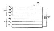
図2には、光電セル200の断面図を示す。光電セル200は、基板210、カソード220、ホールキャリア層230、光活性層240(電子受容性材料および電子供与性材料を含む)、ホールブロック層250、アノード260、および基板270を備える。
FIG. 2 shows a cross-sectional view of the
一般に、使用中、光は基板210の表面に衝突し、基板210、カソード220およびホールキャリア層230を通過する。次いで、この光は光活性層240と相互作用し、光活性層240の電子供与性材料から光活性層240の電子受容性材料へと電子を移動させる。次いで、電子受容性材料によって、電子がホールブロック層250を通じてアノード260へ伝達され、電子供与性材料によって、ホールがホールキャリア層230を通じてカソード220へ移動される。アノード260およびカソード220は、アノード260から負荷を通じてカソード220へ電子が流れるように、外部の負荷を介して電気的に接続されている。
In general, in use, light strikes the surface of the
基板210は一般に透明材料から形成される。基板210を形成可能な代表的な材料には、ポリエチレンテレフタレート、ポリイミド、ポリエチレンナフタレート、ポリマー性炭化水素、セルロースポリマー、ポリカーボネート、ポリアミド、ポリエーテルおよびポリエーテルケトンが含まれる。一定の実施形態では、ポリマーはフッ素化ポリマーであってよい。一部の実施形態では、ポリマー材料の組み合わせが用いられる。一定の実施形態では、基板210の異なる領域は、異なる材料から形成されてよい。
The
一般に、基板210は、可撓性、半剛性または剛性(例えば、ガラスなど)であってよい。一部の実施形態では、基板210の曲げ弾性率は約5,000MPa未満である。一定の実施形態では、基板210の異なる領域は、可撓性、半剛性または不撓性であってよい(例えば、1つ以上の可撓性領域と異なる1つ以上の半剛性領域、1つ以上の可撓性領域と異なる1つ以上の不撓性領域など)。
In general, the
通常、基板210の厚さは、約1μm以上(例えば、約5μm以上、約10μm以上)、約1,000μm以下(例えば、約500μm以下、約300μm以下、約200μm以下、約100μm以下、約50μm以下)、またはその両方である。
In general, the thickness of the
一般に、基板210は有色または無色であってよい。一部の実施形態では、基板210のうちの1つ以上の部分は有色であり、基板210のうちの異なる1つ以上の部分は無色である。
In general, the
基板210は、1つの平坦面(例えば、光の衝突面)を備えてもよく、2つの平坦面(例えば、光の衝突面および対向面)を備えてもよく、あるいは平坦面を備えなくてもよい。基板210の非平坦面は、例えば、湾曲面または段を有する面であってよい。一部の実施形態では、基板210の非平坦面はパターンを形成されている(例えば、フレネルレンズ、レンチキュラーレンズまたはレンチキュラープリズムを形成するようなパターンの形成された段を備える)。
The
一般に、カソード220は所望に応じて任意の適切な形状を有してよい。一部の実施形態では、カソード220は、上述のものなど、複数の導電性線(すなわち、グリッド電極)から形成されてよい。一部の実施形態では、カソード220はメッシュ電極を含んでよい。メッシュ電極の例は、共通して所有する同時継続中の米国特許出願公開第20040187911号および第20060090791号明細書に記載されている。それらの内容を引用によって本明細書に援用する。
In general, the
ホールキャリア層230は、一般に、光電セル200に用いられる厚さにて、カソード220へホールを移動させるとともに、カソード220への電子の移動をほぼ阻止する材料から形成される。ホールキャリア層230を形成可能な材料の例には、ポリチオフェン(例えば、PEDOT)、ポリアニリン、ポリビニルカルバゾール、ポリフェニレン、ポリフェニルビニレン、ポリシラン、ポリチエニレンビニレン、ポリイソチアナフタレン、およびそれらの共重合体が含まれる。一部の実施形態では、ホールキャリア層230は、半導体高分子と組み合わせて用いられるドーパントを含むことが可能である。ドーパントの例には、ポリ(スチレンスルホン酸)、スルホン酸重合体、またはフッ素化ポリマー(例えば、フッ素化イオン交換ポリマー)が含まれる。一部の実施形態では、ホールキャリア層230を形成するために用いられ得る材料には、チタン酸化物、亜鉛酸化物、タングステン酸化物、モリブデン酸化物、銅酸化物、ストロンチウム銅酸化物、またはストロンチウムチタン酸化物など、金属酸化物が含まれる。金属酸化物は、ドーピングが行われていなくても、ドーパントによるドーピングが行われていてもよい。金属酸化物のドーパントの例には、フッ化物、塩化物、臭化物および沃化物の塩または酸が含まれる。一部の実施形態では、ホールキャリア層230を形成するために用いられ得る材料には、炭素同素体(例えば、カーボンナノチューブ)が含まれる。炭素同素体はポリマーバインダーに埋め込まれてよい。一部の実施形態では、ホールキャリア層230は、上述のホールキャリア材料の組み合わせを含んでよい。一部の実施形態では、ホールキャリア材料はナノ粒子の形態であってよい。ナノ粒子は、球状、円筒状、または棹状の形状など、任意の適切な形状を有してよい。
The
一般に、ホールキャリア層230の厚さ(すなわち、光活性層240に接触しているホールキャリア層230の表面と、ホールキャリア層230に接触しているカソード220の表面との間の距離)は、所望の通りに変更されてよい。通常、ホールキャリア層230の厚さは、0.01μm以上(例えば、約0.05μm以上、約0.1μm以上、約0.2μm以上、約0.3μm以上、もしくは約0.5μm以上)、約5μm以下(例えば、約3μm以下、約2μm以下、もしくは約1μm以下)またはその両方である。一部の実施形態では、ホールキャリア層230の厚さは約0.01マイクロメートル〜約0.5マイクロメートルである。
In general, the thickness of the hole carrier layer 230 (ie, the distance between the surface of the
光活性層240は、一般に、電子受容性材料(例えば、有機電子受容性材料)および電子供与性材料(例えば、有機電子供与性材料)を含む。
電子受容性材料の例には、フラーレン、無機ナノ粒子、オキサジアゾール、ディスコティック液晶、カーボンナノロッド、無機ナノロッド、電子を受容可能な部位もしくは安定なアニオンを形成可能な部位を含むポリマー(例えば、CN基含有ポリマー、CF3基含有ポリマー)またはそれらの組み合わせが含まれる。一部の実施態様では、電子受容性材料は置換フラーレン(例えば、PCBM)である。一部の実施形態では、光活性層240において複数の電子受容性材料の組み合わせが用いられてよい。
Examples of electron-accepting materials include fullerenes, inorganic nanoparticles, oxadiazoles, discotic liquid crystals, carbon nanorods, inorganic nanorods, polymers containing sites capable of accepting electrons or forming stable anions (eg, CN group-containing polymer, CF 3 group-containing polymer) or a combination thereof. In some embodiments, the electron-accepting material is a substituted fullerene (eg, PCBM). In some embodiments, a combination of multiple electron accepting materials may be used in the
電子供与性材料の例には、ポリチオフェン、ポリアニリン、ポリビニルカルバゾール、ポリフェニレン、ポリフェニルビニレン、ポリシラン、ポリチエニレンビニレン、ポリイソチアナフタレン、ポリシクロペンタジチオフェン、ポリシラシクロペンタジチオフェン、ポリシクロペンタジチアゾール、ポリチアゾロチアゾール、ポリチアゾール、ポリベン
ゾチアジアゾール、ポリ(チオフェンオキシド)、ポリ(シクロペンタジチオフェンオキシド)、ポリチアジアゾロキノキサリン、ポリベンゾイソチアゾール、ポリベンゾチアゾール、ポリチエノチオフェン、ポリ(チエノチオフェンオキシド)、ポリジチエノチオフェン、ポリ(ジチエノチオフェンオキシド)、ポリテトラヒドロイソインドールおよびそれらの共重合体など、共役ポリマーが含まれる。一部の実施形態では、電子供与性材料は、ポリチオフェン(例えば、ポリ(3ヘキシルチオフェン))、ポリシクロペンタジチオフェン、およびそれらの共重合体であってよい。一定の実施形態では、光活性層240において複数の電子供与性材料の組み合わせが用いられてよい。
Examples of electron donating materials include polythiophene, polyaniline, polyvinylcarbazole, polyphenylene, polyphenylvinylene, polysilane, polythienylene vinylene, polyisothiaphthalene, polycyclopentadithiophene, polysilacyclopentadithiophene, polycyclopenta Dithiazole, polythiazolothiazole, polythiazole, polybenzothiadiazole, poly (thiophene oxide), poly (cyclopentadithiophene oxide), polythiadiazoloquinoxaline, polybenzoisothiazole, polybenzothiazole, polythienothiophene, poly (Thienothiophene oxide), polydithienothiophene, poly (dithienothiophene oxide), polytetrahydroisoindole and copolymers thereof Over it is included. In some embodiments, the electron donating material may be polythiophene (eg, poly (3 hexylthiophene)), polycyclopentadithiophene, and copolymers thereof. In certain embodiments, a combination of multiple electron donating materials may be used in the
一部の実施形態では、電子供与性材料または電子受容性材料は、第1のコモノマー繰返し単位と、第1のコモノマー繰返し単位とは異なる第2のコモノマー繰返し単位とを有するポリマーを含んでよい。第1のコモノマー繰返し単位は、シクロペンタジチオフェン部位、シラシクロペンタジチオフェン部位、シクロペンタジチアゾール部位、チアゾロチアゾール部位、チアゾール部位、ベンゾチアジアゾール部位、チオフェンオキシド部位、シクロペンタジチオフェンオキシド部位、ポリチアジアゾロキノキサリン部位、ベンゾイソチアゾール部位、ベンゾチアゾール部位、チエノチオフェン部位、チエノチオフェンオキシド部位、ジチエノチオフェン部位、ジチエノチオフェンオキシド部位、またはテトラヒドロイソインドール部位を含んでよい。 In some embodiments, the electron donating material or electron accepting material may comprise a polymer having a first comonomer repeat unit and a second comonomer repeat unit that is different from the first comonomer repeat unit. The first comonomer repeat unit includes a cyclopentadithiophene moiety, a silacyclopentadithiophene moiety, a cyclopentadithiazole moiety, a thiazolothiazole moiety, a thiazole moiety, a benzothiadiazole moiety, a thiophene oxide moiety, a cyclopentadithiophene oxide moiety, It may contain a polythiadiazoloquinoxaline moiety, a benzoisothiazole moiety, a benzothiazole moiety, a thienothiophene moiety, a thienothiophene oxide moiety, a dithienothiophene moiety, a dithienothiophene oxide moiety, or a tetrahydroisoindole moiety.
一部の実施形態では、第1のコモノマー繰返し単位はシクロペンタジチオフェン部位を含む。一部の実施形態では、シクロペンタジチオフェン部位は、C1〜C20のアルキル、C1〜C20のアルコキシ、C3〜C20のシクロアルキル、C1〜C20のヘテロシクロアルキル、アリール、ヘテロアリール、ハロ、CN、OR、C(O)R、C(O)OR、およびSO2Rからなる群から選択される1つ以上の置換基によって置換されている。Rは、H、C1〜C20のアルキル、C1〜C20のアルコキシ、アリール、ヘテロアリール、C3〜C20のシクロアルキル、またはC1〜C20のヘテロシクロアルキルである。例えば、シクロペンタジチオフェン部位は、ヘキシル、2−エチルヘキシル、または3,7−ジメチルオクチルによって置換されてよい。一定の実施形態では、シクロペンタジチオフェン部位は4位が置換されている。一部の実施形態では、第1のコモノマー繰返し単位は、化学式(1)のシクロペンタジチオフェン部位を含んでよい。 In some embodiments, the first comonomer repeat unit comprises a cyclopentadithiophene moiety. In some embodiments, the cyclopentadithiophene moiety is C 1 -C 20 alkyl, C 1 -C 20 alkoxy, C 3 -C 20 cycloalkyl, C 1 -C 20 heterocycloalkyl, aryl. Substituted by one or more substituents selected from the group consisting of:, heteroaryl, halo, CN, OR, C (O) R, C (O) OR, and SO 2 R. R is, H, a heterocycloalkyl C 1 -C 20 alkyl, a C 1 -C 20 alkoxy, aryl, heteroaryl, cycloalkyl C 3 -C 20 or C 1 -C 20,. For example, the cyclopentadithiophene moiety may be substituted by hexyl, 2-ethylhexyl, or 3,7-dimethyloctyl. In certain embodiments, the cyclopentadithiophene moiety is substituted at the 4-position. In some embodiments, the first comonomer repeat unit may comprise a cyclopentadithiophene moiety of formula (1).

化学式(1)において、H、C1〜C20のアルキル、C1〜C20のアルコキシ、C3〜C20のシクロアルキル、C1〜C20のヘテロシクロアルキル、アリール、ヘテロアリール、ハロ、CN、OR、C(O)R、C(O)OR、またはSO2Rの各々。Rは、H、C1〜C20のアルキル、C1〜C20のアルコキシ、アリール、ヘテロアリール、C3〜C20のシクロアルキル、またはC1〜C20のヘテロシクロアルキルである。例えば、R1,R2は各々独立に、ヘキシル、2−エチルヘキシル、または3,7−ジメチルオクチルであってよい。 In the chemical formula (1), H, C 1 ~C 20 alkyl, a C 1 -C 20 alkoxy, C 3 cycloalkyl -C 20, heterocycloalkyl C 1 -C 20, aryl, heteroaryl, halo, Each of CN, OR, C (O) R, C (O) OR, or SO 2 R. R is, H, a heterocycloalkyl C 1 -C 20 alkyl, a C 1 -C 20 alkoxy, aryl, heteroaryl, cycloalkyl C 3 -C 20 or C 1 -C 20,. For example, R 1 and R 2 may each independently be hexyl, 2-ethylhexyl, or 3,7-dimethyloctyl.
アルキルは飽和であっても不飽和であってもよく、分岐鎖であっても直鎖であってもよい。C1〜C20のアルキルは、1〜20個の炭素原子(例えば、1,2,3,4,5,
6,7,8,9,10,11,12,13,14,15,16,17,18,19,20個の炭素原子)を含む。アルキルの部位の例には、−CH3,−CH2−,−CH2=CH2−,−CH2−CH=CH2および分岐した−C3H7が含まれる。アルコキシは分岐鎖であっても直鎖であってもよく、飽和であっても不飽和であってもよい。C1〜C20のアルコキシは、酸素原子と、1〜20個の炭素原子(例えば、1,2,3,4,5,6,7,8,9,10,11,12,13,14,15,16,17,18,19,20個の炭素原子)とを含む。アルコキシ部位の例には、−OCH3および−OCH=CH−CH3が含まれる。シクロアルキルは飽和であっても不飽和であってもよい。C3〜C20のシクロアルキルは、3〜20個の炭素原子(例えば、3,4,5,6,7,8,9,10,11,12,13,14,15,16,17,18,19,20個の炭素原子)を含む。シクロアルキル部位の例には、シクロヘキシルおよびシクロヘキセン−3−イルが含まれる。また、ヘテロシクロアルキルも飽和であっても不飽和であってもよい。C3〜C20のヘテロシクロアルキルは、1つ以上の環ヘテロ原子(例えば、O,N,S)と、3〜20個の炭素原子(例えば、3,4,5,6,7,8,9,10,11,12,13,14,15,16,17,18,19,20個の炭素原子)とを含む。ヘテロシクロアルキル部位の例には、4−テトラヒドロピラニルおよび4−ピラニルが含まれる。アリールは1つ以上の芳香環を含んでよい。アリール部位の例には、フェニル、フェニレン、ナフチル、ナフチレン、ピレニル、アントリル、およびフェナントリルが含まれる。ヘテロアリールは1つ以上の芳香環を含んでよく、この環のうちの1つ以上は1つ以上の環ヘテロ原子(例えば、O,N,S)を含む。ヘテロアリール部位の例には、フリル、フリレン、フルオレニル、ピロリル、チエニル、オキサゾールイル、イミダゾールイル、チアゾールイル、ピリジル、ピリミジニル、キナゾリニル、キノリル、イソキノリル、およびインドールイルが含まれる。
Alkyl may be saturated or unsaturated and may be branched or linear. C 1 -C 20 alkyl is 1 to 20 carbon atoms (eg 1, 2, 3, 4, 5,
6, 7, 8, 9, 10, 11, 12, 13, 14, 15, 16, 17, 18, 19, 20 carbon atoms). Examples of sites alkyl, -CH 3, -CH 2 -, - CH 2 = CH 2 -, - CH 2 -CH = CH 2 and branched -C 3 H 7 are included. Alkoxy may be branched or straight chain and may be saturated or unsaturated. Alkoxy of C 1 -C 20 is an oxygen atom, 1 to 20 carbon atoms (e.g., 1,2,3,4,5,6,7,8,9,10,11,12,13,14 , 15, 16, 17, 18, 19, 20 carbon atoms). Examples of alkoxy moieties include —OCH 3 and —OCH═CH—CH 3 . Cycloalkyls can be saturated or unsaturated. C 3 -C 20 cycloalkyl has 3 to 20 carbon atoms (eg, 3, 4, 5, 6, 7, 8, 9, 10, 11, 12, 13, 14, 15, 16, 17, 18, 19, and 20 carbon atoms). Examples of cycloalkyl moieties include cyclohexyl and cyclohexen-3-yl. Heterocycloalkyl may also be saturated or unsaturated. Heterocycloalkyl C 3 -C 20 can include one or more ring heteroatoms (e.g., O, N, S) and, 3 to 20 carbon atoms (e.g., 3,4,5,6,7,8 , 9, 10, 11, 12, 13, 14, 15, 16, 17, 18, 19, 20 carbon atoms). Examples of heterocycloalkyl moieties include 4-tetrahydropyranyl and 4-pyranyl. Aryl may contain one or more aromatic rings. Examples of aryl moieties include phenyl, phenylene, naphthyl, naphthylene, pyrenyl, anthryl, and phenanthryl. A heteroaryl may contain one or more aromatic rings, one or more of the rings containing one or more ring heteroatoms (eg, O, N, S). Examples of heteroaryl moieties include furyl, furylene, fluorenyl, pyrrolyl, thienyl, oxazolyl, imidazolyl, thiazolyl, pyridyl, pyrimidinyl, quinazolinyl, quinolyl, isoquinolyl, and indolyl.
本明細書において言及されるアルキル、アルコキシ、シクロアルキル、ヘテロシクロアルキル、アリール、およびヘテロアリールには、特に指定のない場合、置換部位と無置換部位との両方が含まれる。シクロアルキル、ヘテロシクロアルキル、アリール、およびヘテロアリールに対する置換基の例には、C1〜C20のアルキル、C3〜C20のシクロアルキル、C1〜C20のアルコキシ、アリール、アリールオキシ、ヘテロアリール、ヘテロアリールオキシ、アミノ、C1〜C10のアルキルアミノ、C1〜C20のジアルキルアミノ、アリールアミノ、ジアリールアミノ、ヒドロキシル、ハロゲン、チオ、C1〜C10のアルキルチオ、アリールチオ、C1〜C10のアルキルスルホニル、アリールスルホニル、シアノ、ニトロ、アシル、アシルオキシ、カルボキシル、およびカルボン酸エステルが含まれる。アルキルに対する置換基の例には、C1〜C20のアルキルを除く上述の置換基全てが含まれる。また、シクロアルキル、ヘテロシクロアルキル、アリール、およびヘテロアリールには、縮合した基が含まれる。 Alkyl, alkoxy, cycloalkyl, heterocycloalkyl, aryl, and heteroaryl referred to herein include both substituted and unsubstituted sites unless otherwise specified. Cycloalkyl, heterocycloalkyl, aryl, and Examples of substituents for the heteroaryl, C 1 alkyl ~C 20, C 3 ~C 20 cycloalkyl, C 1 of -C 20 alkoxy, aryl, aryloxy, heteroaryl, heteroaryloxy, amino, C 1 -C 10 alkylamino, dialkylamino of C 1 -C 20, arylamino, diarylamino, hydroxyl, halogen, thio, alkylthio of C 1 -C 10, arylthio, C alkylsulfonyl of 1 -C 10, aryl sulfonyl, include cyano, nitro, acyl, acyloxy, carboxyl, and carboxylic ester. Examples of substituents for alkyl, includes all the above substituents except the alkyl C 1 -C 20 is. Cycloalkyl, heterocycloalkyl, aryl, and heteroaryl also include fused groups.
第2のコモノマー繰返し単位は、ベンゾチアジアゾール部位、チアジアゾロキノキサリン部位、シクロペンタジチオフェンオキシド部位、ベンゾイソチアゾール部位、ベンゾチアゾール部位、チオフェンオキシド部位、チエノチオフェン部位、チエノチオフェンオキシド部位、ジチエノチオフェン部位、ジチエノチオフェンオキシド部位、テトラヒドロイソインドール部位、フルオレン部位、シロール部位、シクロペンタジチオフェン部位、フルオレノン部位、チアゾール部位、セレノフェン部位、チアゾロチアゾール部位、シクロペンタジチアゾール部位、ナフトチアジアゾール部位、チエノピラジン部位、シラシクロペンタジチオフェン部位、オキサゾール部位、イミダゾール部位、ピリミジン部位、ベンゾオキサゾール部位、またはベンゾイミダゾール部位を含んでよい。一部の実施形態では、第2のコモノマー繰返し単位は、3,4−ベンゾ−1,2,5−チアジアゾール部位である。 The second comonomer repeat unit comprises a benzothiadiazole moiety, a thiadiazoloquinoxaline moiety, a cyclopentadithiophene oxide moiety, a benzisothiazole moiety, a benzothiazole moiety, a thiophene oxide moiety, a thienothiophene moiety, a thienothiophene oxide moiety, a dithienothiophene Site, dithienothiophene oxide site, tetrahydroisoindole site, fluorene site, silole site, cyclopentadithiophene site, fluorenone site, thiazole site, selenophene site, thiazolothiazole site, cyclopentadithiazole site, naphthothiadiazole site, thienopyrazine site Site, silacyclopentadithiophene site, oxazole site, imidazole site, pyrimidine site, benzoxazole site, or It may include zone imidazole site. In some embodiments, the second comonomer repeat unit is a 3,4-benzo-1,2,5-thiadiazole moiety.
一部の実施形態では、第2のコモノマー繰返し単位は、化学式(2)のベンゾチアジア
ゾール部位、化学式(3)のチアジアゾロキノキサリン部位、化学式(4)のシクロペンタジチオフェン二酸化物部位、化学式(5)のシクロペンタジチオフェン一酸化物部位、化学式(6)のベンゾイソチアゾール部位、化学式(7)のベンゾチアゾール部位、化学式(8)のチオフェンジオキサイド部位、化学式(9)のシクロペンタジチオフェンジオキサイド部位、化学式(10)のシクロペンタジチオフェンテトラオキサイド部位、化学式(11)のチエノチオフェン部位、化学式(12)のチエノチオフェンテトラオキサイド部位、化学式(13)のジチエノチオフェン部位、化学式(14)のジチエノチオフェンジオキサイド部位、化学式(15)のジチエノチオフェンテトラオキサイド部位、化学式(16)のテトラヒドロイソインドール部位、化学式(17)のチエノチオフェンジオキサイド部位、化学式(18)のジチエノチオフェンジオキサイド部位、化学式(19)のフルオレン部位、化学式(20)のシロール部位、化学式(21)のシクロペンタジチオフェン部位、化学式(22)のフルオレノン部位、化学式(23)のチアゾール部位、化学式(24)のセレノフェン部位、化学式(25)のチアゾロチアゾール部位、化学式(26)のシクロペンタジチアゾール部位、化学式(27)のナフトチアジアゾール部位、化学式(28)のチエノピラジン部位、化学式(29)のシラシクロペンタジチオフェン部位、化学式(30)のオキサゾール部位、化学式(31)のイミダゾール部位、化学式(32)のピリミジン部位、化学式(33)のベンゾオキサゾール部位、または化学式(34)のベンゾイミダゾール部位を含んでよい。
In some embodiments, the second comonomer repeat unit comprises a benzothiadiazole moiety of formula (2), a thiadiazoloquinoxaline moiety of formula (3), a cyclopentadithiophene dioxide moiety of formula (4), 5) cyclopentadithiophene monoxide moiety, benzisothiazole moiety of formula (6), benzothiazole moiety of formula (7), thiophene dioxide moiety of formula (8), cyclopentadithiophene of formula (9) Dioxide moiety, cyclopentadithiophene tetraoxide moiety of chemical formula (10), thienothiophene moiety of chemical formula (11), thienothiophene tetraoxide moiety of chemical formula (12), dithienothiophene moiety of chemical formula (13), chemical formula (14) ) Dithienothiophene dioxide moiety, chemical formula ( 5) Dithienothiophene tetraoxide moiety of Formula (16), Tetrahydroisoindole moiety of Formula (16), Thienothiophene dioxide moiety of Formula (17), Dithienothiophene dioxide moiety of Formula (18), Fluorene moiety of Formula (19) , A silole moiety of chemical formula (20), a cyclopentadithiophene moiety of chemical formula (21), a fluorenone moiety of chemical formula (22), a thiazole moiety of chemical formula (23), a selenophene moiety of chemical formula (24), and a thiazole of chemical formula (25). Zolothiazole moiety, cyclopentadithiazole moiety of chemical formula (26), naphthothiadiazole moiety of chemical formula (27), thienopyrazine moiety of chemical formula (28), silacyclopentadithiophene moiety of chemical formula (29), oxazole of chemical formula (30) Site, chemical formula (31 Imidazole sites, pyrimidine sites of the formula (32) may comprise a benzimidazole site benzoxazole site of Formula (33) or formula (34).
上述の化学式では、X,Yは各々独立に、CH2,OまたはSであり;R5,R6は各々独立に、H、C1〜C20のアルキル、C1〜C20のアルコキシ、C3〜C20のシクロアルキル、C1〜C20のヘテロシクロアルキル、アリール、ヘテロアリール、ハロ、CN、OR、C(O)R、C(O)OR、またはSO2Rであって、Rは、H、C1〜C20のアルキル、C1〜C20のアルコキシ、アリール、ヘテロアリール、C3〜C20のシクロアルキル、またはC1〜C20のヘテロシクロアルキルであり;R7,R8は各々独立に、H、C1〜C20のアルキル、C1〜C20のアルコキシ、アリール、ヘテロ
アリール、C3〜C20のシクロアルキル、またはC3〜C20のヘテロシクロアルキルである。一部の実施形態では、第2のコモノマー繰返し単位は、化学式(2)のベンゾチアジアゾール部位を含んでよく、R5,R6の各々はHである。
In the above chemical formula, X and Y are each independently CH 2 , O or S; R 5 and R 6 are each independently H, C 1 to C 20 alkyl, C 1 to C 20 alkoxy, cycloalkyl C 3 -C 20, heterocycloalkyl C 1 -C 20, aryl, heteroaryl, halo, CN, oR, C (O ) R, C (O) oR, or a SO 2 R, R is H, C 1 -C 20 alkyl, C 1 -C 20 alkoxy, aryl, heteroaryl, C 3 -C 20 cycloalkyl, or C 1 -C 20 heterocycloalkyl; R 7 , R 8 are each independently H, C 1 -C 20 alkyl, C 1 -C 20 alkoxy, aryl, heteroaryl, C 3 -C 20 cycloalkyl, or C 3 -C 20 heterocycloalkyl. It is a kill. In some embodiments, the second comonomer repeat unit may comprise a benzothiadiazole moiety of formula (2), and each of R 5 and R 6 is H.
第2のコモノマー繰返し単位は、3つ以上のチオフェン部位を含んでよい。一部の実施形態では、1つ以上のチオフェン部位は、C1〜C20のアルキル、C1〜C20のアルコキシ、アリール、ヘテロアリール、C3〜C20のシクロアルキル、およびC3〜C20のヘテロシクロアルキルから選択される1つ以上の置換基によって置換されている。一定の実施形態では、第2のコモノマー繰返し単位は5つのチオフェン部位を含む。 The second comonomer repeat unit may include more than two thiophene moieties. In some embodiments, one or more thiophene moieties are C 1 -C 20 alkyl, C 1 -C 20 alkoxy, aryl, heteroaryl, C 3 -C 20 cycloalkyl, and C 3 -C. Substituted by one or more substituents selected from 20 heterocycloalkyl. In certain embodiments, the second comonomer repeat unit comprises 5 thiophene moieties.
ポリマーは、チオフェン部位またはフルオレン部位を含む第3のコモノマー繰返し単位をさらに含んでよい。一部の実施形態では、チオフェンまたはフルオレン部位は、C1〜C20のアルキル、C1〜C20のアルコキシ、アリール、ヘテロアリール、C3〜C20のシクロアルキル、およびC3〜C20のヘテロシクロアルキルから選択される1つ以上の置換基によって置換されている。 The polymer may further comprise a third comonomer repeat unit comprising a thiophene moiety or a fluorene moiety. In some embodiments, the thiophene or fluorene moiety is a C 1 -C 20 alkyl, C 1 -C 20 alkoxy, aryl, heteroaryl, C 3 -C 20 cycloalkyl, and C 3 -C 20 Substituted by one or more substituents selected from heterocycloalkyl.
一部の実施形態では、ポリマーは、第1のコモノマー繰返し単位、第2のコモノマー繰返し単位、および第3のコモノマー繰返し単位の任意の組み合わせによって形成されてよい。一定の実施形態では、ポリマーは、第1のコモノマー繰返し単位、第2のコモノマー繰返し単位および第3のコモノマー繰返し単位のうちのいずれかを含むホモポリマーであってよい。 In some embodiments, the polymer may be formed by any combination of a first comonomer repeat unit, a second comonomer repeat unit, and a third comonomer repeat unit. In certain embodiments, the polymer may be a homopolymer comprising any of a first comonomer repeat unit, a second comonomer repeat unit, and a third comonomer repeat unit.
一部の実施形態では、ポリマーは次の化学式の通りである。 In some embodiments, the polymer is as follows:
ここで、nは1より大きい整数であってよい。
本明細書において言及したポリマーを調製するためのモノマーは、非芳香属の二重結合と、1つ以上の不斉中心とを含んでよい。したがって、それらはラセミ化合物およびラセミ混合物、単一のエナンチオマー、個々のジアステレオマー、ジアステレオマーの混合物、ならびにcis−またはtrans−異性体の形態として生成する場合がある。そのような異性体の形態は全て想定される。
Here, n may be an integer greater than 1.
Monomers for preparing the polymers mentioned herein may contain non-aromatic double bonds and one or more asymmetric centers. Thus, they may be produced as racemates and racemic mixtures, single enantiomers, individual diastereomers, mixtures of diastereomers, and cis- or trans-isomer forms. All such isomeric forms are envisioned.
上述のポリマーは、共通して所有する同時継続中の米国特許出願第11/601,374号明細書に記載されているものなど、当技術において知られている方法によって調製可能である。その内容を引用によって本明細書に援用する。例えば、共重合体は、遷移金属触媒の存在下、2つのアルキルスズ基を含む1つ以上のコモノマーと、2つのハロ基を含
む1つ以上のコモノマーとの間のクロスカップリング反応によって調製可能である。別の例として、共重合体は、遷移金属触媒の存在下、2つのホウ酸基を含む1つ以上のコモノマーと、2つのハロ基を含む1つ以上のコモノマーとの間のクロスカップリング反応によって調製可能である。コモノマーは、米国特許出願第11/486,536号明細書、コッポ(Coppo)らによる、Macromolecules,2003年、第36巻、p.2705−2711、およびカート(Kurt)らによる、J.Heterocycl.Chem.、1970年、第6巻、p.629に記載されているものなど、当技術において知られている方法によって調製可能である。その内容を引用によって本明細書に援用する。
The above-described polymers can be prepared by methods known in the art, such as those described in commonly owned co-pending US patent application Ser. No. 11 / 601,374. The contents of which are incorporated herein by reference. For example, a copolymer can be prepared by a cross-coupling reaction between one or more comonomers containing two alkyltin groups and one or more comonomers containing two halo groups in the presence of a transition metal catalyst. is there. As another example, a copolymer is a cross-coupling reaction between one or more comonomers containing two boric acid groups and one or more comonomers containing two halo groups in the presence of a transition metal catalyst. Can be prepared. Comonomers are described in US patent application Ser. No. 11 / 486,536, Coppo et al., Macromolecules, 2003, 36, p. 2705-2711, and by Kurt et al. Heterocycl. Chem. 1970, Vol. 6, p. Can be prepared by methods known in the art, such as those described in US Pat. The contents of which are incorporated herein by reference.
理論によって拘束されるものではないが、上述のポリマーの利点は、それらのポリマーの吸収波長が、他のほとんどの従来のポリマーには到達可能でない電磁スペクトルの赤色領域および近赤外領域(例えば、650〜800nm)へと偏移していることであると考えられる。そのようなポリマーが従来のポリマーと共に光電セルへ組み込まれると、セルがスペクトルのこの領域の光を吸収することが可能となり、それによってセルの電流および効率は増大する。 While not being bound by theory, the advantages of the above-described polymers are that their absorption wavelengths are not reachable by most other conventional polymers in the red and near infrared regions of the electromagnetic spectrum (e.g., 650-800 nm). When such a polymer is incorporated into a photocell with a conventional polymer, the cell can absorb light in this region of the spectrum, thereby increasing the cell current and efficiency.
一般に、光活性層240は、光活性層に衝突する光子を吸収して対応する電子およびホールを形成する際に比較的効率的であるのに充分なだけ厚く、このホールおよび電子が移動する際に比較的効率的であるのに充分なだけ薄い。一定の実施形態では、光活性層240の厚さは、0.05μm以上(例えば、約0.1μm以上、約0.2μm以上、もしくは約0.3μm以上)、約1μm以下(例えば、約0.5μm以下もしくは約0.4μm以下)、またはその両方である。一部の実施形態では、光活性層240の厚さは、約0.1μm〜約0.2μmである。
In general, the
ホールブロック層250は、一般に、光電セル200に用いる厚さにて、アノード260へ電子を移動させるとともに、アノード260へのホールの移動をほぼ阻止する材料から形成される。ホールブロック層250を形成可能な材料の例には、LiF、アミン(例えば、第1級、第2級、または第3級アミン)、および金属酸化物(例えば、亜鉛酸化物またはチタン酸化物)が含まれる。
The
通常、ホールブロック層250の厚さは、0.02μm以上(例えば、約0.03μm以上、約0.04μm以上、もしくは約0.05μm以上)、約0.5μm以下(例えば、約0.4μm以下、約0.3μm以下、約0.2μm以下、もしくは約0.1μm以下)、またはその両方である。
Usually, the thickness of the
アノード260は、一般に、上述の導電性材料のうちの1つ以上など、導電性材料から形成される。一部の実施形態では、アノード260は導電性材料の組み合わせから形成される。一定の実施形態では、アノード260はメッシュ電極から形成可能である。
The
基板270は基板210と同一であってもよく、異なっていてもよい。一部の実施形態では、基板270は、上述のものなど1つ以上の適切なポリマーから形成可能である。
図3には、2個の準セル302,304を有するタンデム型の光電セル300を示す。準セル302は、カソード320、ホールキャリア層330、第1の光活性層340および再結合層342を含む。準セル304は、再結合層342、第2の光活性層344、ホールブロック層350およびアノード360を含む。外部負荷は、カソード320およびアノード360を介して光電セル300に接続されている。生産工程および所望のデバイス構成に応じて、一定の層の電子/ホール伝導率を変更すること(例えば、ホールブロック層350をホールキャリア層に変更すること)によって、準セルの電流が逆転されてよい。そうすることによって、タンデム型セルは、タンデム型セルにおいて準セルが電気的
に直列にまたは並列に相互接続されるように、設計されることが可能である。
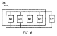
The
FIG. 3 shows a tandem
再結合層は、タンデム型セルにおいて、第1の準セルから生成した電子が第2の準セルから生成されたホールと再結合する層を表す。再結合層342は、通常、p型半導体材料およびn型半導体材料を含む。一般に、n型半導体材料は選択的に電子を移動させ、p型半導体材料は選択的にホールを移動させる。その結果、第1の準セルから生成された電子は第2の準セルから生成されたホールとn型半導体材料とp型半導体材料との界面において再結合する。
The recombination layer represents a layer in which electrons generated from the first quasi-cell recombine with holes generated from the second quasi-cell in the tandem cell.
一部の実施形態では、p型半導体材料はポリマー、金属酸化物またはその両方を含む。p型半導体ポリマーの例には、ポリチオフェン(例えば、ポリ(3,4−エチレンジオキシチオフェン)(PEDOT))、ポリアニリン、ポリビニルカルバゾール、ポリフェニレン、ポリフェニルビニレン、ポリシラン、ポリチエニレンビニレン、ポリイソチアナフタレン、ポリシクロペンタジチオフェン、ポリシラシクロペンタジチオフェン、ポリシクロペンタジチアゾール、ポリチアゾロチアゾール、ポリチアゾール、ポリベンゾチアジアゾール、ポリ(チオフェンオキシド)、ポリ(シクロペンタジチオフェンオキシド)、ポリチアジアゾロキノキサリン、ポリベンゾイソチアゾール、ポリベンゾチアゾール、ポリチエノチオフェン、ポリ(チエノチオフェンオキシド)、ポリジチエノチオフェン、ポリ(ジチエノチオフェンオキシド)、ポリテトラヒドロイソインドールおよびそれらの共重合体が含まれる。金属酸化物は、本質的なp型半導体(例えば、銅酸化物、ストロンチウム銅酸化物、もしくはストロンチウムチタン酸化物)であってもよく、またはドーパントによるドーピング後にp型半導体を形成する金属酸化物(例えば、pドープした亜鉛酸化物もしくはpドープしたチタン酸化物)であってもよい。ドーパントの例には、フッ化物、塩化物、臭化物および沃化物の塩または酸が含まれる。一部の実施形態では、金属酸化物はナノ粒子の形態で用いられてよい。 In some embodiments, the p-type semiconductor material includes a polymer, a metal oxide, or both. Examples of p-type semiconductor polymers include polythiophene (eg, poly (3,4-ethylenedioxythiophene) (PEDOT)), polyaniline, polyvinylcarbazole, polyphenylene, polyphenylvinylene, polysilane, polythienylene vinylene, polyisothia. Naphthalene, polycyclopentadithiophene, polysilacyclopentadithiophene, polycyclopentadithiazole, polythiazolothiazole, polythiazole, polybenzothiadiazole, poly (thiophene oxide), poly (cyclopentadithiophene oxide), polythi Asiazoloquinoxaline, polybenzoisothiazole, polybenzothiazole, polythienothiophene, poly (thienothiophene oxide), polydithienothiophene, poly (dithienothiopheneoxy) ), Poly tetrahydroisoindole and copolymers thereof. The metal oxide may be an intrinsic p-type semiconductor (eg, copper oxide, strontium copper oxide, or strontium titanium oxide) or a metal oxide that forms a p-type semiconductor after doping with a dopant ( For example, p-doped zinc oxide or p-doped titanium oxide) may be used. Examples of dopants include fluoride, chloride, bromide and iodide salts or acids. In some embodiments, the metal oxide may be used in the form of nanoparticles.
一部の実施形態では、n型半導体材料は、チタン酸化物、亜鉛酸化物、タングステン酸化物、モリブデン酸化物、およびそれらの組み合わせなど、金属酸化物を含む。金属酸化物はナノ粒子の形態で用いられてよい。他の実施形態では、n型半導体材料は、フラーレン、無機ナノ粒子、オキサジアゾール、ディスコティック液晶、カーボンナノロッド、無機ナノロッド、CN基含有ポリマー、CF3基含有ポリマーおよびそれらの組み合わせから選択される材料を含む。 In some embodiments, the n-type semiconductor material includes a metal oxide, such as titanium oxide, zinc oxide, tungsten oxide, molybdenum oxide, and combinations thereof. The metal oxide may be used in the form of nanoparticles. In other embodiments, the n-type semiconductor material is selected from fullerenes, inorganic nanoparticles, oxadiazoles, discotic liquid crystals, carbon nanorods, inorganic nanorods, CN group-containing polymers, CF 3 group-containing polymers, and combinations thereof. Contains materials.
一部の実施形態では、p型半導体材料およびn型半導体材料は、1つの層へと混合される。一定の実施形態では、再結合層は、p型半導体材料を含む1つの層と、n型半導体材料を含む別の層との2つの層を含む。 In some embodiments, the p-type semiconductor material and the n-type semiconductor material are mixed into one layer. In certain embodiments, the recombination layer includes two layers: one layer that includes a p-type semiconductor material and another layer that includes an n-type semiconductor material.
一部の実施形態では、再結合層342は、約30重量%以上(例えば、約40重量%以上もしくは約50重量%以上)、約70重量%以下(例えば、約60重量%以下または約50重量%以下)のp型半導体材料を含む。一部の実施形態では、再結合層342は、約30重量%以上(例えば、約40重量%以上もしくは約50重量%以上)、約70重量%以下(例えば、約60重量%以下または約50重量%以下)のn型半導体材料を含む。
In some embodiments, the
再結合層342は、一般に、再結合層342上に塗布される溶媒からその下の層が保護されるのに充分な厚さを有する。一部の実施形態では、再結合層342の厚さは、約10nm以上(例えば、約20nm以上、約50nm以上、もしくは約100nm以上)、約500nm以下(例えば、約200nm以下、約150nm以下、もしくは約100nm以下)またはその両方である。
The
一般に、再結合層342は、ほぼ透明である。例えば、タンデム型の光電セル300に
用いられる厚さにて、再結合層342は、光電セルの動作中に用いられる波長または波長範囲(例えば、約350nm〜約1,000nm)にて、入射光線の約70%以上(例えば、約75%以上、約80%以上、約85%以上、または約90%以上)を透過させることが可能である。
In general, the
再結合層342は、一般に、充分に低い抵抗率を有する。一部の実施形態では、再結合層342の抵抗率は、約1×10⁶オーム/□以下(例えば、約5×105オーム/□以下、約2×105オーム/□以下、または約1×105オーム/□以下)である。
The
理論によって拘束されるものではないが、再結合層342は、光電セル300における2つの準セル(例えば、一方は、カソード320、ホールキャリア層330、光活性層340および再結合層342を含み、他方は、再結合層342、光活性層344、ホールブロック層350およびアノード360を含む)の間の共通の電極と見なすことができると考えられる。一部の実施形態では、再結合層342は、上述のものなど、導電性メッシュ材料を含んでよい。導電性メッシュ材料は、準セルに同じ極性(p型またはn型)の選択的な接点を提供し、負荷へ電子を移動させるため、導電性が高く透明な層を提供することが可能である。
Without being bound by theory,
一部の実施形態では、再結合層342は、n型半導体材料およびp型半導体材料のブレンドを光活性層上に塗布することによって調製可能である。例えば、n型半導体およびp型半導体は、最初に分散液または溶液を形成するように溶媒へ一緒に分散または溶解され、次いで、再結合層を形成するように、その分散液または溶液が光活性層上にコーティングされる。
In some embodiments, the
一部の実施形態では、再結合層342は、タンデム型セルの機能に必要な電子的および光学的性質を有する2つ以上の層を含んでよい。例えば、再結合層342は、n型半導体材料を含む層と、p型半導体材料を含む層とを含む。そのような実施形態では、再結合層342は、2つの層の界面において混合されたn型半導体材料およびp型半導体材料の層を含んでよい。
In some embodiments, the
一部の実施形態では、2層の再結合層は、n型半導体材料の層とp型半導体材料の層とを別々に塗布することによって調製可能である。例えば、チタン酸化物ナノ粒子がn型半導体材料として用いられるとき、チタン酸化物ナノ粒子の層は、(1)溶媒(例えば、無水アルコール)中に前駆物質(例えば、チタン塩)を分散させて分散液を形成すること、(2)光活性層上に分散液をコーティングすること、(3)分散液を水和させてチタン酸化物層を形成すること、および(4)チタン酸化物層を乾燥させること、によって形成可能である。別の例として、ポリマー(例えば、PEDOT)がp型半導体として用いられるときには、ポリマー層は、最初に溶媒(例えば、無水アルコール)中にポリマーを溶解して溶液を形成し、次いで、その溶液を光活性層上にコーティングすることによって形成可能である。 In some embodiments, the two recombination layers can be prepared by applying a layer of n-type semiconductor material and a layer of p-type semiconductor material separately. For example, when titanium oxide nanoparticles are used as an n-type semiconductor material, the layer of titanium oxide nanoparticles (1) has a precursor (eg, titanium salt) dispersed in a solvent (eg, anhydrous alcohol). Forming a dispersion; (2) coating the dispersion on the photoactive layer; (3) hydrating the dispersion to form a titanium oxide layer; and (4) forming a titanium oxide layer. It can be formed by drying. As another example, when a polymer (eg, PEDOT) is used as a p-type semiconductor, the polymer layer first dissolves the polymer in a solvent (eg, anhydrous alcohol) to form a solution, then the solution is It can be formed by coating on the photoactive layer.
タンデム型セル300における他の部品は、上述の光電セル200におけるものと同一であってよい。
一部の実施形態では、タンデム型セルにおいて準セルは電気的に直列に相互接続されている。直列に接続されるとき、一般に、層は図3に示す順序であってよい。一定の実施形態では、タンデム型セルにおいて準セルは電気的に並列相互接続されている。並列に相互接続されるとき、2個の準セルを有するタンデム型セルは、次の層、すなわち、第1のカソード、第1のホールキャリア層、第1の光活性層、第1のホールブロック層(アノードとして機能することが可能である)、第2のホールブロック層(アノードとして機能することが可能である)、第2の光活性層、第2のホールキャリア層および第2のカソードを
含むことが可能である。そのような実施形態では、第1および第2のホールブロック層は、2つの別個の層であってもよく、1つの単一の層であってもよい。第1のおよび第2のホールブロック層の伝導率が充分でない場合、必要な伝導率を提供する追加の層(例えば、導電性メッシュ層)が挿入されてもよい。
Other components in the
In some embodiments, the quasi-cells are electrically interconnected in series in a tandem cell. When connected in series, generally the layers may be in the order shown in FIG. In certain embodiments, the quasi-cells are electrically interconnected in parallel in a tandem cell. When interconnected in parallel, a tandem cell having two quasi-cells has the following layers: a first cathode, a first hole carrier layer, a first photoactive layer, a first hole block A layer (which can function as an anode), a second hole blocking layer (which can function as an anode), a second photoactive layer, a second hole carrier layer and a second cathode. It is possible to include. In such an embodiment, the first and second hole blocking layers may be two separate layers or one single layer. If the conductivity of the first and second hole blocking layers is not sufficient, an additional layer (eg, a conductive mesh layer) that provides the necessary conductivity may be inserted.
一部の実施形態では、タンデム型セルは2個を超える準セル(例えば、3,4,5,6,7,8,9,10またはより多くの準セル)を含んでよい。一定の実施形態では、一部の準セルが電気的に直列に相互接続されていることが可能であり、一部の準セルが電気的に並列に相互接続されていることが可能である。 In some embodiments, a tandem cell may include more than two quasicells (eg, 3, 4, 5, 6, 7, 8, 9, 10, or more quasicells). In certain embodiments, some quasi-cells can be electrically interconnected in series, and some quasi-cells can be electrically interconnected in parallel.
一般に、図2,3に記載の光電セルの各層を調製する方法は、所望に応じて異なってよい。一部の実施形態では、層は液体ベースのコーティング処理によって調製可能である。本明細書において言及する用語「液体ベースのコーティング処理」は、液体ベースのコーティング組成物を用いる処理を表す。液体ベースのコーティング組成物の例には、溶液、分散液または懸濁液が含まれる。液体ベースのコーティング処理は、次の処理、すなわち、溶液コーティング、インクジェット印刷、スピンコーティング、ディップコーティング、ナイフコーティング、バーコーティング、スプレーコーティング、ローラコーティング、スロットコーティング、グラビアコーティング、フレキソ印刷またはスクリーン印刷のうちの1つ以上を用いることによって実行可能である。液体ベースのコーティング処理の例は、例えば、共通して所有する同時継続中の米国特許出願第60/888,704号明細書に記載されている。その内容を引用によって本明細書に援用する。一定の実施形態では、層は、化学蒸着法または物理蒸着法など、気相ベースのコーティング処理を介して調製可能である。 In general, the method of preparing each layer of the photovoltaic cell described in FIGS. 2 and 3 may vary as desired. In some embodiments, the layer can be prepared by a liquid-based coating process. The term “liquid-based coating process” referred to herein refers to a process using a liquid-based coating composition. Examples of liquid based coating compositions include solutions, dispersions or suspensions. The liquid-based coating process consists of the following processes: solution coating, ink jet printing, spin coating, dip coating, knife coating, bar coating, spray coating, roller coating, slot coating, gravure coating, flexographic printing or screen printing This can be done by using one or more of An example of a liquid-based coating process is described, for example, in commonly owned co-pending US Patent Application No. 60 / 888,704. The contents of which are incorporated herein by reference. In certain embodiments, the layer can be prepared via a vapor phase based coating process, such as chemical vapor deposition or physical vapor deposition.
一部の実施形態では、図2,3に記載の光電セルは、ロール・ツー・ロール法などの連続的製造工程により調整可能であり、これによって製造コストが有意に減少する。ロール・ツー・ロール法の例は、例えば、共通して所有する同時継続中の米国特許出願公開第2005−0263179号明細書に記載されている。その内容を引用によって本明細書に援用する。 In some embodiments, the photovoltaic cell described in FIGS. 2 and 3 can be tuned by a continuous manufacturing process such as a roll-to-roll process, which significantly reduces manufacturing costs. An example of a roll-to-roll process is described, for example, in commonly owned co-pending US Patent Application Publication No. 2005-0263179. The contents of which are incorporated herein by reference.
一定の実施形態について開示したが、他の実施形態も可能である。
一部の実施形態では、複数の光電セルを電気的に接続し、光電システムを形成することが可能である。一例として、図4には、光電セル420を含むモジュール410を備える光電システム400の概略図を示す。光電セル420は電気的に直列に接続されており、システム400は負荷430へ電気的に接続されている。別の例として、図5は、光電セル520を含むモジュール510を有する光電システム500の概略図である。光電セル520は電気的に並列に接続されており、システム500は負荷530へ電気的に接続されている。一部の実施形態では、光電システムにおける一部(例えば、全部)の光電セルが1つ以上の共通の基板を有してよい。一定の実施形態では、光電システムにおける一部の光電セルは電気的に直列に接続されており、その光電システムにおいて、一部の光電セルは電気的に並列に接続されている。
While certain embodiments have been disclosed, other embodiments are possible.
In some embodiments, multiple photovoltaic cells can be electrically connected to form a photovoltaic system. As an example, FIG. 4 shows a schematic diagram of a
特許請求の範囲には他の実施形態が存在する。 Other embodiments are within the scope of the claims.
Claims (38)
複数の導電性線を含む第1の電極と、
第2の電極と、
第1の電極と第2の電極との間にあって、電子供与性材料および電子受容性材料を含む光活性層と、を備え、
前記導電性線は第1の部分において第1の幅を有し、第2の部分において第1の幅と異なる第2の幅を有し、前記物品は光電セルとして構成されている、物品。 Goods,
A first electrode including a plurality of conductive wires;
A second electrode;
A photoactive layer between the first electrode and the second electrode and comprising an electron donating material and an electron accepting material,
The article, wherein the conductive line has a first width in a first portion and a second width different from the first width in a second portion, and the article is configured as a photocell.
複数の導電性線を含む第1の電極と、
第2の電極と、
第1の電極と第2の電極との間の第1および第2の光活性層と、を備え、第1の光活性層および第2の光活性層のうちの1つ以上は電子供与性材料および電子受容性材料を含み、
前記導電性線は第1の部分において第1の幅を有し、第2の部分において第1の幅と異なる第2の幅を有し、前記システムは光電システムとして構成されている、システム。 A system,
A first electrode including a plurality of conductive wires;
A second electrode;
First and second photoactive layers between the first electrode and the second electrode, wherein one or more of the first photoactive layer and the second photoactive layer are electron donating Including materials and electron-accepting materials,
The conductive line has a first width in a first portion and a second width different from the first width in a second portion, and the system is configured as a photoelectric system.
Applications Claiming Priority (2)
| Application Number | Priority Date | Filing Date | Title |
|---|---|---|---|
| US78056006P | 2006-03-09 | 2006-03-09 | |
| PCT/US2007/063669 WO2007104039A2 (en) | 2006-03-09 | 2007-03-09 | Photovoltaic cells |
Publications (1)
| Publication Number | Publication Date |
|---|---|
| JP2009529792A true JP2009529792A (en) | 2009-08-20 |
Family
ID=38475874
Family Applications (1)
| Application Number | Title | Priority Date | Filing Date |
|---|---|---|---|
| JP2008558548A Withdrawn JP2009529792A (en) | 2006-03-09 | 2007-03-09 | Photocell |
Country Status (4)
| Country | Link |
|---|---|
| EP (1) | EP1997219A4 (en) |
| JP (1) | JP2009529792A (en) |
| KR (1) | KR20080104181A (en) |
| WO (1) | WO2007104039A2 (en) |
Cited By (3)
| Publication number | Priority date | Publication date | Assignee | Title |
|---|---|---|---|---|
| JP2007273939A (en) * | 2005-09-06 | 2007-10-18 | Kyoto Univ | Organic thin-film photoelectric converter and method of manufacturing the same |
| JP2011514913A (en) * | 2008-02-05 | 2011-05-12 | ビーエーエスエフ ソシエタス・ヨーロピア | Semiconductor materials made from rylene- (π-acceptor) copolymers |
| JP2014504809A (en) * | 2011-02-03 | 2014-02-24 | メルク パテント ゲーエムベーハー | Photocell |
Families Citing this family (2)
| Publication number | Priority date | Publication date | Assignee | Title |
|---|---|---|---|---|
| KR100986159B1 (en) * | 2008-12-22 | 2010-10-07 | 한국기계연구원 | Organic solar cell enhancing energy conversion efficiency and method for preparing the same |
| KR101564330B1 (en) | 2009-10-15 | 2015-10-29 | 삼성전자주식회사 | Solar cell having organic nanowires |
Family Cites Families (6)
| Publication number | Priority date | Publication date | Assignee | Title |
|---|---|---|---|---|
| US7022910B2 (en) * | 2002-03-29 | 2006-04-04 | Konarka Technologies, Inc. | Photovoltaic cells utilizing mesh electrodes |
| US6706963B2 (en) * | 2002-01-25 | 2004-03-16 | Konarka Technologies, Inc. | Photovoltaic cell interconnection |
| EP1450420A1 (en) * | 2003-02-24 | 2004-08-25 | Sony International (Europe) GmbH | Discotic liquid crystal based electronic device using interdigit structure electrode |
| GB0309355D0 (en) * | 2003-04-24 | 2003-06-04 | Univ Cambridge Tech | Organic electronic devices incorporating semiconducting polymer |
| JP4232597B2 (en) * | 2003-10-10 | 2009-03-04 | 株式会社日立製作所 | Silicon solar cell and manufacturing method thereof |
| JP2005353904A (en) * | 2004-06-11 | 2005-12-22 | Sharp Corp | Electrode, method for forming the same, solar cell, and method for manufacturing the same |
-
2007
- 2007-03-09 WO PCT/US2007/063669 patent/WO2007104039A2/en active Application Filing
- 2007-03-09 KR KR1020087024622A patent/KR20080104181A/en not_active Application Discontinuation
- 2007-03-09 JP JP2008558548A patent/JP2009529792A/en not_active Withdrawn
- 2007-03-09 EP EP07758241A patent/EP1997219A4/en not_active Withdrawn
Cited By (4)
| Publication number | Priority date | Publication date | Assignee | Title |
|---|---|---|---|---|
| JP2007273939A (en) * | 2005-09-06 | 2007-10-18 | Kyoto Univ | Organic thin-film photoelectric converter and method of manufacturing the same |
| JP2011514913A (en) * | 2008-02-05 | 2011-05-12 | ビーエーエスエフ ソシエタス・ヨーロピア | Semiconductor materials made from rylene- (π-acceptor) copolymers |
| JP2014504809A (en) * | 2011-02-03 | 2014-02-24 | メルク パテント ゲーエムベーハー | Photocell |
| US9515274B2 (en) | 2011-02-03 | 2016-12-06 | Merck Patent Gmbh | Photovoltaic cells |
Also Published As
| Publication number | Publication date |
|---|---|
| EP1997219A2 (en) | 2008-12-03 |
| WO2007104039A9 (en) | 2007-12-13 |
| KR20080104181A (en) | 2008-12-01 |
| WO2007104039A3 (en) | 2008-12-24 |
| EP1997219A4 (en) | 2009-07-22 |
| WO2007104039A2 (en) | 2007-09-13 |
Similar Documents
| Publication | Publication Date | Title |
|---|---|---|
| JP5649954B2 (en) | Articles configured as photovoltaic cells | |
| US8975512B2 (en) | Tandem photovoltaic cells | |
| US20070193621A1 (en) | Photovoltaic cells | |
| JP5265380B2 (en) | Photovoltaic system and method of configuring the same | |
| JP5651606B2 (en) | Photocell having a plurality of electron donors | |
| JP5613303B2 (en) | Organic photovoltaic cell | |
| EP2261980B1 (en) | Tandem photovoltaic cells | |
| EP2321861B1 (en) | Novel photoactive co- polymers | |
| US8178779B2 (en) | Organic photovoltaic cells | |
| US20070267055A1 (en) | Tandem Photovoltaic Cells | |
| WO2010005622A2 (en) | Telescoping devices | |
| JP2009529792A (en) | Photocell | |
| WO2010083161A1 (en) | Photovoltaic module | |
| WO2010138414A1 (en) | Reflective multilayer electrode | |
| ES2352219T3 (en) | PHOTOVOLTAIC CELLS IN TANDEM. | |
| WO2009009634A1 (en) | Photovoltaic cells with a diffractive layer |
Legal Events
| Date | Code | Title | Description |
|---|---|---|---|
| A300 | Application deemed to be withdrawn because no request for examination was validly filed |
Free format text: JAPANESE INTERMEDIATE CODE: A300 Effective date: 20100511 |