JP2009524237A - Method and apparatus for improved stability in probing systems - Google Patents
Method and apparatus for improved stability in probing systems Download PDFInfo
- Publication number
- JP2009524237A JP2009524237A JP2008551251A JP2008551251A JP2009524237A JP 2009524237 A JP2009524237 A JP 2009524237A JP 2008551251 A JP2008551251 A JP 2008551251A JP 2008551251 A JP2008551251 A JP 2008551251A JP 2009524237 A JP2009524237 A JP 2009524237A
- Authority
- JP
- Japan
- Prior art keywords
- actuation force
- relative
- acceleration
- component
- sensor
- Prior art date
- Legal status (The legal status is an assumption and is not a legal conclusion. Google has not performed a legal analysis and makes no representation as to the accuracy of the status listed.)
- Pending
Links
Images


Classifications
-
- G—PHYSICS
- G01—MEASURING; TESTING
- G01R—MEASURING ELECTRIC VARIABLES; MEASURING MAGNETIC VARIABLES
- G01R31/00—Arrangements for testing electric properties; Arrangements for locating electric faults; Arrangements for electrical testing characterised by what is being tested not provided for elsewhere
- G01R31/28—Testing of electronic circuits, e.g. by signal tracer
- G01R31/2851—Testing of integrated circuits [IC]
- G01R31/2886—Features relating to contacting the IC under test, e.g. probe heads; chucks
- G01R31/2891—Features relating to contacting the IC under test, e.g. probe heads; chucks related to sensing or controlling of force, position, temperature
-
- G—PHYSICS
- G01—MEASURING; TESTING
- G01R—MEASURING ELECTRIC VARIABLES; MEASURING MAGNETIC VARIABLES
- G01R31/00—Arrangements for testing electric properties; Arrangements for locating electric faults; Arrangements for electrical testing characterised by what is being tested not provided for elsewhere
- G01R31/26—Testing of individual semiconductor devices
-
- G—PHYSICS
- G01—MEASURING; TESTING
- G01R—MEASURING ELECTRIC VARIABLES; MEASURING MAGNETIC VARIABLES
- G01R1/00—Details of instruments or arrangements of the types included in groups G01R5/00 - G01R13/00 and G01R31/00
- G01R1/02—General constructional details
- G01R1/06—Measuring leads; Measuring probes
-
- H—ELECTRICITY
- H01—ELECTRIC ELEMENTS
- H01L—SEMICONDUCTOR DEVICES NOT COVERED BY CLASS H10
- H01L22/00—Testing or measuring during manufacture or treatment; Reliability measurements, i.e. testing of parts without further processing to modify the parts as such; Structural arrangements therefor
Abstract
動き擾乱の存在下で半導体デバイスのボンディング・パッドに対して、ウエハの整列を自動的に、かつ、正確に維持するための改良された方法及び装置が提供される。本発明の一態様の一実施形態では、多数の加速度センサ及び/又は速度センサからの情報を組み入れたフィードバック制御システムを使用して、動き擾乱の存在下で所望の接触位置が維持される。 An improved method and apparatus is provided for automatically and accurately maintaining wafer alignment relative to semiconductor device bonding pads in the presence of motion disturbances. In one embodiment of one aspect of the invention, a feedback control system incorporating information from multiple acceleration and / or velocity sensors is used to maintain a desired contact position in the presence of motion disturbances.
Description
本発明は、半導体デバイスなどのターゲットと電気接触するように設計された、プローブ先端などの複数の接触点を有する、ウエハ・プローバなどのシステムをプロービングするシステムに関する。 The present invention relates to a system for probing a system, such as a wafer prober, having a plurality of contact points, such as probe tips, designed to be in electrical contact with a target, such as a semiconductor device.
集積回路は、シリコン・ウエハなどの半導体基板上に作製されることが多い。シリコン・ウエハは、通常、直径が150か、200か、又は300ミリメートルで、かつ、ほぼ2ミリメートル厚であるシリコンの円形薄板である。通常、1つウエハは、格子パターンで形成される集積回路である多数のデバイスを有する。各デバイスは、多数の回路要素の層と外部ボンディング・パッド(及び、任意選択で、試験パッド)の集合体からなる。ボンディング・パッドは、アルミニウムで普通作られ、通常3ミル平方の小さな箇所であり、最終的に、ピン・リードに対するデバイスの接続部の役をする。 Integrated circuits are often fabricated on a semiconductor substrate such as a silicon wafer. Silicon wafers are typically circular thin plates of silicon that are 150, 200, or 300 millimeters in diameter and approximately 2 millimeters thick. A single wafer typically has a number of devices that are integrated circuits formed in a lattice pattern. Each device consists of a collection of multiple circuit element layers and external bonding pads (and optionally, test pads). Bond pads are usually made of aluminum and are typically a small area of 3 mil square and ultimately serve as the device's connection to the pin leads.
プロービングは、プローブ先端とボンディング・パッド又は他のパッドとの間で電気的(抵抗)接続を行うために、ボンディング・パッドをプローブ先端に接触させることを含む。先端の下でのパッドの正確な位置決めは、パッドに対して損傷が生じることを回避すると共に、良好な電気接触を確実にする所望の接触圧力を維持するために必要である(ピンは、実際には、通常の大気条件下でパッドを覆って形成する外部酸化物層を通して「スクラビング」しなければならない)。 Probing involves bringing the bonding pad into contact with the probe tip to make an electrical (resistive) connection between the probe tip and the bonding pad or other pad. Accurate positioning of the pad under the tip is necessary to avoid damage to the pad and to maintain the desired contact pressure to ensure good electrical contact (the pin is actually Must be “scrubbed” through an outer oxide layer formed over the pad under normal atmospheric conditions).
床振動(通常、10〜30Hz)、プローブ・ユニットに対する偶然の打撃、又は、他の誘発振動の供給源などの外部擾乱は、プローブ先端とパッドの正確な位置決めを乱す可能性がある。プローブ・システム内のコンポーネント間の接合部及び接続部の固有の曲げ特性又は非剛性特定が与えられると、異なる周波数と振幅でユニットの異なる部分に振動が生じる場合がある。接続部における曲げ変形は、ウエハ表面と、通常、ピンに似ているプローブ先端との間の非補償的相対変位をもたらすであろう。 External disturbances such as floor vibrations (usually 10-30 Hz), accidental strikes on the probe unit, or other sources of induced vibrations can disturb the precise positioning of the probe tip and pad. Given the inherent bending characteristics or non-rigidity of joints and connections between components in the probe system, vibrations may occur in different parts of the unit at different frequencies and amplitudes. Bending deformation at the connection will result in uncompensated relative displacement between the wafer surface and the probe tip, which usually resembles a pin.
相対変位は、接続部の剛性を増すことによって、又は、床とユニットとの間を隔離させることによって減少する可能性がある。これらの方法は、システムの重量を増加させ、それにより、(たとえば、全ての設置における隔離特性を変更することを必要とすることによる)コストと、こうした擾乱に対する周波数領域での感度の両方を増加させるという欠点を有する。従来技術のシステムは、通常、非常に重く、深い地下土台にしっかりとボルト止めされた、いわゆる、隔離テーブルを含む。これらのテーブルは、反応相殺又は反応性隔離(たとえば、ウエハ・ステッパについて行われている)をもたらす。専用アクチュエータを有する振動補償を含む能動隔離テーブルも存在する。しかし、全てのこれらの従来技術のシステムは、総額が非常に高く(800,000〜1,000,000ドル)、プロービング・ユニットの可搬性を排除する複雑な設置手順を伴う(可搬性は、たとえば、鋳造所における、非内製生産についての大きな利点である可能性がある)。他方、既存の可搬型プロービング・システムは、軽量であり、隔離テーブルを組み込まず、本来、剛性が低い。現在、能動的な振動抑制又は補償を組み込む従来技術の可搬型プロービング・システムは存在しない。システムがウエハ上でダイからダイへ非常に迅速に進める動作を可能にすることによって、補正がスループットを改善することになるため、能動的擾乱補償を組み込む可搬型プロービング・ユニットは、非常に望ましいことになる。 Relative displacement can be reduced by increasing the stiffness of the connection or by isolating the floor from the unit. These methods increase the weight of the system, thereby increasing both cost (eg, by requiring the isolation characteristics to be changed in every installation) and frequency domain sensitivity to such disturbances. Has the disadvantage of Prior art systems typically include so-called isolation tables that are very heavy and are bolted firmly to a deep underground foundation. These tables provide reactive cancellation or reactive isolation (eg, done for wafer steppers). There are also active isolation tables that include vibration compensation with dedicated actuators. However, all these prior art systems are very expensive ($ 800,000-1,000,000) and involve complex installation procedures that eliminate the portability of the probing unit (portability is For example, it can be a great advantage for non-in-house production at foundries). On the other hand, existing portable probing systems are lightweight, do not incorporate an isolation table and are inherently less rigid. Currently, there are no prior art portable probing systems that incorporate active vibration suppression or compensation. A portable probing unit that incorporates active disturbance compensation is highly desirable because the correction will improve throughput by allowing the system to move very quickly from die to die on the wafer. become.
動き擾乱の存在下で、ウエハ・デバイス上の複数のパッドと複数の接触電極(たとえば、プローブ・カード上のピン)との間の接触位置決めを正確に維持するための、改良された方法及び装置が提供される。本発明の態様の一実施態様によれば、好ましくない動き擾乱(床振動など)を補償するために、加速度センサ及び/又は速度センサが、動きフィードバック制御システム内に統合される。 Improved method and apparatus for accurately maintaining contact positioning between pads on a wafer device and contact electrodes (eg, pins on a probe card) in the presence of motion disturbances Is provided. According to one embodiment of aspects of the present invention, acceleration and / or velocity sensors are integrated into the motion feedback control system to compensate for undesired motion disturbances (such as floor vibrations).
本発明の別の態様の別の実施態様によれば、プローバ・システムのコンポーネント間の異なる加速度又は速度に基づく補償方式が使用される。 In accordance with another embodiment of another aspect of the invention, a compensation scheme based on different accelerations or velocities between components of the prober system is used.
本発明の別の態様のさらに別の実施態様によれば、プローバ・システムのコンポーネント間の相対加速度に基づく補償方式が使用される。 According to yet another embodiment of another aspect of the invention, a compensation scheme based on relative acceleration between components of the prober system is used.
本発明のさらなる実施態様は、制御方式によって決定された補償力を加えるために、ウエハ整列機構内の既存のアクチュエータを使用することを含む。 Further embodiments of the invention include using existing actuators in the wafer alignment mechanism to apply the compensation force determined by the control scheme.
本発明の少なくともいくつかの実施態様によって提供された解決策は、制御及び検知システムによって、動き擾乱を能動的に抑制するか、又は、補償する第1可搬型ウエハ・プローバを提供する。本発明の、これらの、また、他の実施態様、特徴、態様、利点は、添付図面から、また、以下に続く詳細な説明及び添付特許請求の範囲から明らかになるであろう。 The solution provided by at least some embodiments of the present invention provides a first portable wafer prober that actively suppresses or compensates for motion disturbances by a control and sensing system. These and other embodiments, features, aspects and advantages of the present invention will become apparent from the accompanying drawings and from the detailed description and claims that follow.
本発明は、添付図面の図において、制限としてではなく、例として示される。図では、同じ参照は、同様な要素を示す。 The present invention is illustrated by way of example and not limitation in the figures of the accompanying drawings. In the figures, the same reference indicates similar elements.
試験システムにおいてプローブ先端とボンディング・パッドとの間で所望の接触位置を正確に維持するための方法及び装置が開示される。以下の説明では、説明のために、本発明の完全な理解を可能にするために、多数の特定の詳細が述べられる。しかし、本発明が、これらの特定の詳細がない状態で実施されてもよいことが当業者に明らかになるであろう。他の事例では、よく知られている構造や装置は、本発明を不必要に曖昧にすることを回避するために、ブロック図の形態で示される。 A method and apparatus for accurately maintaining a desired contact position between a probe tip and a bonding pad in a test system is disclosed. In the following description, for the purposes of explanation, numerous specific details are set forth in order to provide a thorough understanding of the present invention. However, it will be apparent to those skilled in the art that the present invention may be practiced without these specific details. In other instances, well-known structures and devices are shown in block diagram form in order to avoid unnecessarily obscuring the present invention.
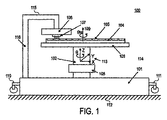
プロービングは、高圧条件下で、プローブ先端が、ボンド・パッドにわたって「スクラビングする」か、又は、摺動するように、ウエハのパッド表面をプローブ先端に接触させることを含む。本発明の考えられる一実施態様では、プローバ・システムは、2つの主要なコンポーネント又はステージ、すなわち、一方はウエハを保持するもの、他方はプローブ・カードからなる。2つのステージは、互いに対して移動し、パッドと先端との間に高圧接触を生成するように結合される。図1は、2つの主要ステージ114と115からなるプロービング・システム100の考えられる1つのこうした実施形態の略図を示す。図示するシステムの2つの主要ステージは、ウエハ・ホルダ・アセンブリ(WHA)ステージ114及びプローブカード・ホルダ・アセンブリ(PHA)ステージ115と呼ばれる。この具体的な例では、WHAステージ114は、X、Y、Z、シータg方向113に沿って移動可能であり、一方、PHAステージ115は、固定のまま保持される。さらに、ウエハ104自体は、WHAステージの保持チャック103に対してシータw方向を中心に回転する。こうして、WHAステージによって支持されるウエハ104は、PHAステージによって支持されるプローブ・カード・ピン107に対して移動することができ、その結果、ピンは、ウエハ104上の任意所与のパッド105に接触させられる。
Probing involves contacting the pad surface of the wafer with the probe tip such that, under high pressure conditions, the probe tip “scrabs” or slides across the bond pad. In one possible embodiment of the invention, the prober system consists of two major components or stages, one holding the wafer and the other a probe card. The two stages move relative to each other and are coupled to create a high pressure contact between the pad and the tip. FIG. 1 shows a schematic diagram of one possible embodiment of a
WHAステージは、いくつかのコンポーネントからなる。いくつかのコンポーネントとは、床112に置かれ、かつ、Zステージ102が、レール(この図では示さず)上で、X及びY方向113に沿って低摩擦で移動することを可能にするX及びYガントリ・システムを含むグラナイト・ベース101、及び、試験用に多数のダイ・パッド105を有するウエハ104を保持することが目的であるチャック103である。チャック103は、ガントリ・システムのZステージ102に接続され、したがって、ガントリ・システムに結合した作動システム108によって、X、Y、Z、シータ方向113に沿って移動可能である。ガントリはまた、以下に述べるセンサ情報を利用する動き制御システムを収容する。
The WHA stage consists of several components. Some components are X that are placed on the
PHAステージは、ウエハ・パッド105に接触するために、プローブ・カード・ピン107を向けることが目的であるプローブ・カード・チャック106からなる。プローブ・カード・チャックは、グラナイト・ベース101に直接接続される構造116によって支持される。この具体的な例では、PHAステージは、移動機構を持たず、固定である。
The PHA stage consists of a
プロービング・システム100は、ホイール110、111などのホイールで移動してもよい。ホイールは、グラナイト・ベースが床に(たとえば、床上に直接か、又は、伸縮自在の脚部上に)載るように引っ込めることができる1組(たとえば、4つ)のホイールであってよく、また、1組のホイールは、プロービング・システム100が、1組のホイールでころがって進むことができるように伸張することもできる。ホイール110と111は、図1で引っ込めた位置で示される。1組のホイールは、プロービング・システム100が、可搬型であることを可能にする。
Probing
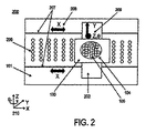
図2は、図1に示すシステムの平面図である。この具体的な例では、Zステージ102が、グラナイト・ベース101上をスムースに移動するのに役立ち、したがって、Zステージ102とグラナイト・ベース101との間の接触摩擦の一部をなくすために、Zステージ102に対して上向きに空気を吹き付ける均等に分布した一連の空気オリフィス206を持つように示されている。こうして、Zステージ102は、グラナイト・ベース101上で「浮上する」と言われる。グラナイト・ベース101上の2つのレール207は、Zステージ102の動きをX方向208に沿って伝える。ブリッジ202は、グラナイト・ベース101の上部に載り、Zステージ102とチャック103を支持し、チャック103は、次に、ウエハ104とその接触パッド105を保持する。チャック103は、2つのモータ(図示せず)によって、グラナイト・ベース101に対してX方向208に沿って(レール207上を)、また、ブリッジ202とレール207を含むガントリ・システム内に収容されるさらなる移動機構(図示せず)によって、ガントリ202に対してY、Z、シータ(θ)方向209に沿って移動する。これは、ウエハ・カード204上の接触パッド205が、考えられる3つの方向X、Y、Z(210)に沿って直線的に、また、ヨー軸(Z軸の周り又はシータ方向210)に沿って回転して効率的に移動することを可能にする。Zステージ102は、ブリッジ202に沿って左右に移動することによって、Y軸に沿って移動する。ブリッジ202は、レール207に結合され、レール207に沿ってXに移動する。
FIG. 2 is a plan view of the system shown in FIG. In this specific example, the Z stage 102 helps to move smoothly over the
典型的なプロービング・システムでは、異なるコンポーネントを接合する接続部は、柔軟性を有する。コンポーネント間の接続部は、完璧に剛性があるわけではない(極端な例として、ガントリは、図2に示す空気テーブルによって持ち上げられ、グラナイト・ベース上で浮上する)ため、システムの一部が擾乱にさらされると、システムのコンポーネント間に振動の又は曲げの相対変位が存在する。曲げ変形は、次に、ウエハ・パッドとプローブ・カード・ピンとの間の非補償的変位を引き起こす場合があり、そのため、性能が低下する。 In a typical probing system, the connection that joins the different components is flexible. The connections between the components are not perfectly rigid (as an extreme example, the gantry is lifted by the air table shown in Figure 2 and floats on the granite base), thus disturbing part of the system Exposure to vibration, there is a relative displacement of vibration or bending between the components of the system. Bending deformation can then cause an uncompensated displacement between the wafer pad and the probe card pin, thus reducing performance.
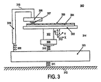
図3は、種々のコンポーネントの一部の間での曲げ接続部を備えるプロービング・システムの考えられる実施形態を示す。いくつかのコンポーネントの間の例示的な非剛性接続部のいくつかが、図3に示される。こうして、Zステージ302とグラナイト・ベース301との間の接合部310は、接合部の曲げ(及び振動)の性質を示すために、ばねシンボル310で示される。同様に、PHAステージ315とWHAステージ314のグラナイト・ベース301との接続部309、及び、グラナイト・ベース301と床312との間の接合部311も同様に、ばねシンボルで示される。実際の物理的なばねは存在しないが、接合部は、これらのばねでモデル化されるか、又は、表されてもよいことが理解されるであろう。
FIG. 3 shows a possible embodiment of a probing system with bending connections between some of the various components. Some of the exemplary non-rigid connections between several components are shown in FIG. Thus, the joint 310 between the
接続部の曲げ剛性を増すことによって、又は、床とシステムとの間に隔離を設けることによって、好ましくない相対変位が減少する可能性がある。これらの方法は、システムの重量の増加を必要とする(それにより、動き擾乱に対して周波数領域における感度が上がる)という欠点、及び、プロービング・システムの設置において隔離特性の変更を必要とするという欠点を有する。好ましくない振動の影響を低減することになる、コストがかからず、複雑さの少ない解決策は、検知・制御システムによって、能動的に、動き擾乱を抑制するか、又は、補償することである。 Undesirable relative displacement can be reduced by increasing the bending stiffness of the connection or by providing isolation between the floor and the system. These methods have the disadvantage of requiring an increase in the weight of the system (thus increasing the sensitivity in the frequency domain to motion disturbances) and the need to change the isolation characteristics in the installation of the probing system Has drawbacks. A low-cost, low-complexity solution that will reduce the effects of unwanted vibrations is to actively suppress or compensate for motion disturbances with a detection and control system. .
本発明の別の態様の考えられる実施形態では、擾乱測定器具が、プロービング・システム上のいくつかの箇所に付加される。たとえば、1つのセンサはグラナイト・ベース上に設置され、別のセンサはガントリ・システム上のXYZ移動機構上に設置され、第3のセンサはプローブ・ピン位置決めインタフェース上に設置される。擾乱振幅と位相の情報は3つの箇所全てで、かつ、異なる方向(X、Y、Z)に沿って連続して測定される。検知情報は、ローパス・フィルタを通して動きコントローラに入力されて、信号内の高周波ノイズがなくされる。コントローラは、その後、相対的な振幅と位相の情報を処理して、移動機構の既存の作動ドライブを通して、X、Y、Z、又はシータ方向において、システムに補償的補正を適用する。その結果得られる動きは、ウエハ基板とプローブ・ピンとの間に、制御されないあらゆる相対変位は存在しない。さらに、ウエハ・チャックが、1つのダイをプロービングし次のダイをプロービングする位置へ移動するときに、加速度計を使用して、反応力(内部擾乱)も相殺することになるため、補正によって、システムはウエハ上でダイからダイへ非常に迅速に進めることが可能になる。 In a possible embodiment of another aspect of the invention, a disturbance measurement instrument is added at several points on the probing system. For example, one sensor is installed on the granite base, another sensor is installed on an XYZ moving mechanism on the gantry system, and a third sensor is installed on the probe pin positioning interface. Disturbance amplitude and phase information is measured continuously at all three locations and along different directions (X, Y, Z). Detection information is input to the motion controller through a low pass filter to eliminate high frequency noise in the signal. The controller then processes the relative amplitude and phase information and applies compensatory corrections to the system in the X, Y, Z, or theta direction through the existing actuation drive of the moving mechanism. The resulting motion does not have any uncontrolled relative displacement between the wafer substrate and the probe pins. In addition, when the wafer chuck is moved to the position where one die is probed and the next die is probed, the accelerometer will also cancel out the reaction force (internal disturbance), so the correction The system can proceed very quickly from die to die on the wafer.
図4は、加速度計がシステム上の3つの異なる箇所に付加された、図3に提示した例示的なプロービング・システムの同じ側面図を示す。ボックスA1412、A2413、A3414は、それぞれ、グラナイト・ベース301、ブリッジ/チャック/ウエハ・アセンブリ402(しっかりと接続されるものと仮定され、したがって、単一振動要素として考えられることができる)、PHAステージ315の動きを測定するためにそれぞれ付加された3つの加速度計を表す。
FIG. 4 shows the same side view of the exemplary probing system presented in FIG. 3, with accelerometers added at three different locations on the system.
これらの3つのセンサの付加は、外部又は内部擾乱によって、これらの3つの箇所のそれぞれで誘発される振動加速度及び/又は速度の大きさ及び位相の定量化を可能にする。同様に、測定を使用して、測定されるコンポーネント間の相対的な、加速度、速度、大きさ、位相を導出することができる。両方のタイプの(個別の、及び、相対的な)測定が、好ましくない変位を補償するための異なる制御方式で使用される。 The addition of these three sensors allows the quantification of magnitude and phase of vibration acceleration and / or velocity induced at each of these three locations by external or internal disturbances. Similarly, measurements can be used to derive relative acceleration, velocity, magnitude, and phase between measured components. Both types of (individual and relative) measurements are used in different control schemes to compensate for undesired displacements.
本発明の同じ態様の別の実施形態では、別法として、速度センサか、速度センサと加速度センサの組合せか、又は、異なる箇所において異なる数のセンサを使用することが可能である。こうしたセンサを使用して、ウエハ・チャックとプローブ・カード・プラットフォームの一方又は両方を移動させるために(ガントリ・システムではなく)ソーヤー・モータを使用するウエハ・プロービング・システム内の動き擾乱を補償してもよいことも理解されるであろう。 In other embodiments of the same aspect of the invention, it is alternatively possible to use a speed sensor, a combination of speed and acceleration sensors, or a different number of sensors at different locations. These sensors are used to compensate for motion disturbances in a wafer probing system that uses a sawer motor (rather than a gantry system) to move one or both of the wafer chuck and probe card platform. It will be understood that it may be.
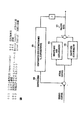
図5は、それぞれ、グラナイト・ベースとガントリとに位置する2つのセンサ501、502からの加速度情報を組み入れた制御システムの考えられる実施形態のブロック図を示す。この特定の実施形態は、本発明の別の態様、すなわち、動作中の接触位置擾乱をなくすように設計された制御方式を示すのに役立つ。図5に示す特に具体的な実施形態では、コントローラは、2つの主要なループ、すなわち、自分自身の位置コントローラ508を有する位置制御ループ513と、自分自身の振動コントローラ509を有する加速度制御ループ514からなる。
FIG. 5 shows a block diagram of a possible embodiment of a control system incorporating acceleration information from two
先に説明したように、Zステージは、ガントリ・システムのブリッジに取り付けられ、グラナイト・ベース上で浮上する。ガントリは、ここでは、図4のブリッジ/チャック/ウエハ・アセンブリ402を備えるものと仮定する。作動モータがガントリを前方へ駆動すると、同じ量の牽引力が、グラナイト・ベースに逆方向に作用することになる(ニュートンの動きの第3法則による)。これは、内部擾乱と考えることができる。同様に、(たとえば、床の揺れによって)ベースに作用する任意の外部擾乱は、ガントリとグラナイト・ベースとの間の牽引力のために、ガントリに現れる。ガントリとベースとの間が非剛性接続であるため、振動相対変位は、こうした擾乱によって誘発される。
As explained above, the Z stage is attached to the bridge of the gantry system and floats on the granite base. The gantry is now assumed to comprise the bridge / chuck /
図5に示す補償方式の設計目的は、ガントリとグラナイト・ベースが共に、同じ振幅と位相を有すること、すなわち、制御システムが、ガントリとベースとの間の相対振動を補償する(又は、なくす)ことを確実にすることである。 The design objective of the compensation scheme shown in FIG. 5 is that both the gantry and the granite base have the same amplitude and phase, ie, the control system compensates (or eliminates) the relative vibration between the gantry and the base. Is to make sure.
本発明のこの態様の特に具体的なこの実施形態のために、グラナイト・ベースと床との間に剛性接続部が存在することが仮定され、両者は、質量MEQと剛性KEQを有する単一ばね質量システムとみなされる。剛性KEQは、ベースとガントリとの間の、図4に示すばね310に相当する。
For this particular embodiment of this aspect of the invention, it is assumed that there is a rigid connection between the granite base and the floor, both of which have a mass M EQ and a stiffness K EQ. Considered a one-spring mass system. The stiffness K EQ corresponds to the
床/ベース構造は、ガントリの質量に対して移動することができ、ガントリの質量は、この具体的な例の場合、質量MGantryを持ち、かつ、それ自身の剛性を持たない線形システムであると仮定される。上記仮定に基づいて、GGantry-on-Graniteと呼ぶ、グラナイト・ベースに対するガントリの動特性(図5のコントローラが、それを抑制するように設計される、ベースとガントリとの間の相対動きを生成することになる)は、伝達関数、すなわち、 The floor / base structure can move relative to the mass of the gantry, which in this particular example is a linear system with mass M Gantry and without its own stiffness. Is assumed. Based on the above assumptions, the Gantry-on-Granite dynamic characteristics of the gantry relative to the granite base (the relative movement between the base and the gantry, which the controller of FIG. 5 is designed to suppress) Will be generated) is the transfer function, ie

ここで、
AccRelative(s)は、ベース511の加速度の読みとガントリ512の加速度の読みを減算することによって得られるベースとガントリとの間の相対加速度503であり、
FActual(s)は、補償力510と所望の制御力505の結合アクションから生じる、ベースとガントリに加えられる制御力504であり、
GGantry(s)は、ガントリの動特性の伝達関数であり、
GGranite(s)は、床/ベースの動特性の伝達関数であり、
here,
Acc Relative (s) is the
F Actual (s) is the
G Gantry (s) is the transfer function of the dynamic characteristics of the gantry,
G Granite (s) is a transfer function of floor / base dynamics,
![]()
![]()
![]()
![]()
ω1とω2の組合せである式(1)の共振(又は、分母のルートを計算することによって得られる極)が与えられると、サーボ・コントローラ(図5では、位置コントローラ508と振動コントローラ509の組合せ)が、指令された位置506の完璧な追従(すなわち、位置誤差507がゼロ)を得ることは難しい。したがって、図5において、所望の制御505信号と相対加速度503信号との間の動特性を線形化する補償510を設計することが望ましい。この場合、サーボ・コントローラは理想的な(ゼロ)誤差制御を持つ。本発明の別の態様では、制御方式の実施形態は、こうした線形化を含む。
Given the resonance of equation (1), which is a combination of ω 1 and ω 2 (or the pole obtained by calculating the denominator route), the servo controller (in FIG. 5,
図6は、ベース602とガントリ603との間の相対動特性604を線形化し、したがって、共振をなくすように設計された、HCompensationと呼ばれる(また、図5の振動コントローラ509と等価な)補償制御601の考えられる実施形態のブロック図を示す。結果として得られる補償605又はFCompensationは、以下のように設計される。
FCompensation=MGantry×AccGranite (2)
ここで、AccGraniteは、グラナイト・ベースの加速度である。
FIG. 6 linearizes the relative dynamic characteristic 604 between the base 602 and the
F Compensation = M Gantry x Acc Granite (2)
Here, Acc Granite is a granite-based acceleration.
式(2)は、所望されるように、共振周波数に感じない。ガントリとベースの相対動特性GGantry-on-Graniteを、式(2)に組み込むと、補償制御HCompensation601は、
Equation (2) does not feel at the resonant frequency as desired. When the gantry-base relative dynamic characteristic G Gantry-on-Granite is incorporated into equation (2), the
![]()
![]()
したがって、その結果得られる補償を有するシステム動特性(式(2)と(3)を式(4)に代入する)は、 Therefore, the resulting system dynamics with compensation (substituting equations (2) and (3) into equation (4)) are:
式(5)の補償を有する相対動特性 Relative dynamics with compensation of equation (5)
![]()
![]()
図7は、図6の加速度ベースの補償制御601が、図5の制御方式全体に組み入れられた(701)ときの、完全な制御ブロック図である。
FIG. 7 is a complete control block diagram when the acceleration-based
任意の方向における、かつ、動き擾乱の存在下での、プローブ・ピンに対するウエハ・パッドの正確でかつ連続した位置決めを達成するために、同じ種類か又は他の種類の複数のセンサの読みを組み込む制御システムの他の実施形態もまた、本発明によって含まれる。同様に、プロービング・システム内での動き擾乱の能動的抑制をもたらす、異なる方法でシステム内の異なるコンポーネントの個々の(非相対的な)又は相対的な加速度を補償する他の方式もまた、本発明によって包含される。 Incorporate multiple sensor readings of the same or other types to achieve accurate and continuous positioning of the wafer pad relative to the probe pins in any direction and in the presence of motion disturbances Other embodiments of the control system are also encompassed by the present invention. Similarly, other schemes that compensate for individual (non-relative) or relative accelerations of different components in the system in different ways, resulting in active suppression of motion disturbances within the probing system, are also available. Covered by the invention.
図8は、WHAステージに関する動き擾乱を補償するために、センサ及び制御システムを利用する試験システムに関わるステップの考えられる実施形態を示すフロー図である。第1操作801として、WHAステージとPHAステージは、所望の接触位置と力が達成されるまで接触させられる。所望の接触位置を維持するために、ガントリとベースとの間の任意の振動(大きさ及び位相)が、連続して測定されて(802)、床の揺れ又はガントリの作動などの動き擾乱による、所望の接触位置の変化が検出される。制御システムは、その後、センサ情報に基づいて必要とされる補正アクションを決定する(803)。補正力は、その後、WHAステージ内に組み込まれたアクチュエータによってガントリに加えられて、好ましくない位置擾乱がなくされ、所望の位置が追従される(804)。所望の位置に対するいずれの擾乱も迅速に補正されることを確実にするために、少なくともいくつかの実施形態では、操作802〜804が、連続して(たとえば、50ミリ秒ごとに)繰り返される。プロービング・プロセスにおいて、新しい組のボンディング・パッドにわたってプローブ先端を位置決めするように、ダイからダイへ進めるために、これらの操作(802〜804)はまた、WHAステージとPHAステージが、互いに対して移動するときに、繰り返し(たとえば、50ミリ秒ごとに)実施される。システムの他のパラメータ及びコンポーネントが、監視され、制御される他の実施形態も可能である。
FIG. 8 is a flow diagram illustrating a possible embodiment of the steps involved in a test system that utilizes sensors and a control system to compensate for motion disturbances related to the WHA stage. As a
本明細書で述べる方法は、ソフトウェア制御下で動作する汎用又は専用コンピュータなどのデータ処理システムによって実施されることができ、ソフトウェアは、種々の読み取り可能媒体に格納されることができる。 The methods described herein can be implemented by a data processing system such as a general purpose or special purpose computer operating under software control, and the software can be stored on a variety of readable media.
本発明の種々の実施形態は、全ウエハを保持するウエハ・チャックを有するウエハ・プローバ、又は、フィルム・フレーム(柔軟性がある)又はストリップ(剛性がある場合がある)上でダイ又はダイスをプロービングするシステムなどの他のタイプのプロービング・システム上で使用されてもよい。 Various embodiments of the present invention provide a wafer prober with a wafer chuck that holds the entire wafer, or a die or die on a film frame (which may be flexible) or a strip (which may be rigid). It may be used on other types of probing systems, such as a probing system.
こうして、擾乱の存在下で、試験システム内で正確なパッド−プローブ接触位置決めを達成し、維持する装置及び方法が提供された。本発明は、特定の例示的な実施形態を参照して述べられたが、添付特許請求の範囲に述べられる本発明のより広範な精神及び範囲から逸脱することなく、これらの実施形態に対して、種々の修正及び変更が行われてもよいことが明らかになるであろう。したがって、仕様及び図面は、制限的ではなく、例証的に考えられる。 Thus, an apparatus and method has been provided for achieving and maintaining accurate pad-probe contact positioning within a test system in the presence of disturbances. Although the invention has been described with reference to particular exemplary embodiments, it is to be understood that these embodiments may be practiced without departing from the broader spirit and scope of the invention as set forth in the appended claims. It will be apparent that various modifications and changes may be made. Accordingly, the specification and drawings are to be regarded as illustrative rather than restrictive.
Claims (18)
前記複数の電気接点を有するデバイスを保持するように構成された第1コンポーネントの少なくとも1つの箇所に結合し、3次元座標系の少なくとも1つの軸に沿って少なくとも1つのパラメータを測定するように構成された少なくとも1つのセンサと、
前記少なくとも1つのセンサから情報を受信するように構成され、かつ、前記情報に基づいて作動力を決定するように構成された、前記第1コンポーネントに結合された制御システムと
を備え、前記作動力が、システムに対する動き擾乱を補償するように前記第1コンポーネントに作用するシステム。 A test system that operates to maintain a relative position between a plurality of contact electrodes and a plurality of electrical contacts,
Coupled to at least one location of a first component configured to hold a device having a plurality of electrical contacts and configured to measure at least one parameter along at least one axis of a three-dimensional coordinate system At least one sensor,
A control system coupled to the first component configured to receive information from the at least one sensor and to determine an actuation force based on the information, the actuation force Operating on the first component to compensate for motion disturbances to the system.
前記複数の接触電極に結合されるデバイスを保持するように構成された第1コンポーネントに結合した少なくとも1つのセンサを使用して3次元座標系の少なくとも1つの軸に沿って少なくとも1つのパラメータを測定するステップと、
前記第1コンポーネントに結合された制御システムを使用して作動力を決定するステップであって、制御システムは、前記少なくとも1つのセンサから情報を受信し、前記情報に基づいて作動力を決定するように構成され、システムに対する動き擾乱を補償するように前記作動力が前記第1コンポーネントに作用する、作動力を決定するステップと
を備える方法。 A method of maintaining positioning of a plurality of contact electrodes with respect to a plurality of pads,
Measuring at least one parameter along at least one axis of a three-dimensional coordinate system using at least one sensor coupled to a first component configured to hold a device coupled to the plurality of contact electrodes And steps to
Determining an actuation force using a control system coupled to the first component, wherein the control system receives information from the at least one sensor and determines the actuation force based on the information. And determining the actuation force, wherein the actuation force acts on the first component to compensate for motion disturbances to the system.
前記複数の接触電極に結合されるデバイスを保持するように構成された第1コンポーネントに結合した少なくとも1つのセンサを使用して3次元座標系の少なくとも1つの軸に沿って少なくとも1つのパラメータを測定するステップと、
前記第1コンポーネントに結合された制御システムを使用して作動力を決定するステップであって、前記制御システムは、前記少なくとも1つのセンサから情報を受信し、前記情報に基づいて作動力を決定するように構成され、システムに対する動き擾乱を補償するように前記作動力が前記第1コンポーネントに作用する、前記作動力を決定するステップと
を含む、機械可読媒体。 A machine-readable medium providing executable computer instructions that when executed by a data processing system causes the system to perform a method of maintaining the positioning of a plurality of contact electrodes with respect to a plurality of pads, the method comprising: ,
Measuring at least one parameter along at least one axis of a three-dimensional coordinate system using at least one sensor coupled to a first component configured to hold a device coupled to the plurality of contact electrodes And steps to
Determining an actuation force using a control system coupled to the first component, the control system receiving information from the at least one sensor and determining an actuation force based on the information Determining the actuation force, wherein the actuation force acts on the first component to compensate for motion disturbances to the system.
Applications Claiming Priority (2)
| Application Number | Priority Date | Filing Date | Title |
|---|---|---|---|
| US11/335,081 US7352198B2 (en) | 2006-01-18 | 2006-01-18 | Methods and apparatuses for improved stabilization in a probing system |
| PCT/US2006/042343 WO2007084205A1 (en) | 2006-01-18 | 2006-10-30 | Methods and apparatuses for improved stabilization in a probing system |
Publications (2)
| Publication Number | Publication Date |
|---|---|
| JP2009524237A true JP2009524237A (en) | 2009-06-25 |
| JP2009524237A5 JP2009524237A5 (en) | 2010-01-14 |
Family
ID=37875700
Family Applications (1)
| Application Number | Title | Priority Date | Filing Date |
|---|---|---|---|
| JP2008551251A Pending JP2009524237A (en) | 2006-01-18 | 2006-10-30 | Method and apparatus for improved stability in probing systems |
Country Status (6)
| Country | Link |
|---|---|
| US (3) | US7352198B2 (en) |
| JP (1) | JP2009524237A (en) |
| KR (1) | KR101297262B1 (en) |
| CN (1) | CN101297205A (en) |
| TW (1) | TWI442067B (en) |
| WO (1) | WO2007084205A1 (en) |
Families Citing this family (21)
| Publication number | Priority date | Publication date | Assignee | Title |
|---|---|---|---|---|
| KR100746364B1 (en) * | 2006-07-28 | 2007-08-06 | 엠텍비젼 주식회사 | Method and apparatus for sharing memory |
| JP2008219174A (en) * | 2007-02-28 | 2008-09-18 | Matsushita Electric Ind Co Ltd | Portable terminal device |
| US20090206229A1 (en) * | 2008-02-15 | 2009-08-20 | Ivan Nesch | Dual vibration isolation apparatus |
| JP5222038B2 (en) * | 2008-06-20 | 2013-06-26 | 東京エレクトロン株式会社 | Probe device |
| DE102008038186A1 (en) * | 2008-08-19 | 2010-02-25 | Suss Microtec Test Systems Gmbh | Probe for the temporary electrical contacting of a solar cell |
| DE102008038184A1 (en) * | 2008-08-19 | 2010-02-25 | Suss Microtec Test Systems Gmbh | Method and device for the temporary electrical contacting of a solar cell |
| US8120304B2 (en) * | 2008-12-12 | 2012-02-21 | Formfactor, Inc. | Method for improving motion times of a stage |
| US8519728B2 (en) * | 2008-12-12 | 2013-08-27 | Formfactor, Inc. | Compliance control methods and apparatuses |
| US8902062B2 (en) * | 2011-01-27 | 2014-12-02 | Honeywell International Inc. | Systems and methods for detection of device displacement and tampering |
| CN102495344B (en) * | 2011-11-11 | 2014-12-17 | 深圳市矽电半导体设备有限公司 | Method and system of grain detecting |
| US9395404B2 (en) * | 2012-12-14 | 2016-07-19 | Infineon Technologies Ag | Method for testing semiconductor chips or semiconductor chip modules |
| US9478237B2 (en) | 2013-09-18 | 2016-10-25 | Seagate Technology Llc | Work piece contact pad with centering feature |
| TWI515442B (en) * | 2013-12-13 | 2016-01-01 | Mpi Corp | Electrical testing machine |
| US9459886B2 (en) | 2014-08-06 | 2016-10-04 | Texas Instruments Incorporated | Autonomous sleep mode |
| US10060475B2 (en) * | 2014-12-24 | 2018-08-28 | Teradyne, Inc. | Braking system |
| JP7069018B2 (en) * | 2016-01-30 | 2022-05-17 | エレクトロ サイエンティフィック インダストリーズ インコーポレーテッド | System isolation and optic bay sealing |
| CN109451763B (en) | 2018-05-16 | 2019-11-08 | 长江存储科技有限责任公司 | Method and system for wafer bonding alignment compensation |
| KR20220067416A (en) | 2020-11-17 | 2022-05-24 | 세메스 주식회사 | Apparatus for driving and apparatus for dispensing droplet using the same |
| EP4027150A1 (en) * | 2021-01-07 | 2022-07-13 | Afore Oy | Testing device and method for reducing vibration in a testing device |
| CN114000192B (en) * | 2021-10-29 | 2023-10-13 | 北京北方华创微电子装备有限公司 | Semiconductor process equipment and method for monitoring wafer position state |
| TWI794002B (en) * | 2022-01-28 | 2023-02-21 | 緯創資通股份有限公司 | Multimedia system and multimedia operation method |
Citations (10)
| Publication number | Priority date | Publication date | Assignee | Title |
|---|---|---|---|---|
| JPH01284793A (en) * | 1988-05-11 | 1989-11-16 | Canon Inc | Substrate support device |
| US5814733A (en) * | 1996-09-12 | 1998-09-29 | Motorola, Inc. | Method of characterizing dynamics of a workpiece handling system |
| JPH11162828A (en) * | 1997-11-21 | 1999-06-18 | Nikon Corp | Projection aligner and projection aligning method |
| JPH11190762A (en) * | 1997-12-26 | 1999-07-13 | Micronics Japan Co Ltd | Manual prober |
| JPH11251381A (en) * | 1998-03-02 | 1999-09-17 | Micronics Japan Co Ltd | Manual prober |
| JP2000216084A (en) * | 1998-11-19 | 2000-08-04 | Nikon Corp | Projection aligner |
| JP2001102279A (en) * | 1999-09-27 | 2001-04-13 | Nikon Corp | Stage device and aligner |
| JP2001110717A (en) * | 1999-10-13 | 2001-04-20 | Nikon Corp | Stage and stage contrl method, and aligner |
| JP2004152916A (en) * | 2002-10-29 | 2004-05-27 | Nec Corp | Inspecting device and inspecting method of semiconductor device |
| JP2005300381A (en) * | 2004-04-13 | 2005-10-27 | Seiko Epson Corp | Prove inspecting device and probe inspecting device body |
Family Cites Families (25)
| Publication number | Priority date | Publication date | Assignee | Title |
|---|---|---|---|---|
| JP3219844B2 (en) * | 1992-06-01 | 2001-10-15 | 東京エレクトロン株式会社 | Probe device |
| JPH07111215B2 (en) * | 1992-08-26 | 1995-11-29 | 鹿島建設株式会社 | Vibration isolation device |
| JP2963603B2 (en) * | 1993-05-31 | 1999-10-18 | 東京エレクトロン株式会社 | Probe device alignment method |
| US5473698A (en) * | 1993-11-23 | 1995-12-05 | Garnjost; Kenneth D. | Method of controlling the application of counter-vibration to a structure |
| US5644245A (en) * | 1993-11-24 | 1997-07-01 | Tokyo Electron Limited | Probe apparatus for inspecting electrical characteristics of a microelectronic element |
| US5550483A (en) * | 1994-11-18 | 1996-08-27 | International Business Machines | High speed test probe positioning system |
| DE69630509T2 (en) * | 1995-08-11 | 2004-08-12 | Ebara Corp. | Magnetic levitation damping device |
| US6040700A (en) * | 1997-09-15 | 2000-03-21 | Credence Systems Corporation | Semiconductor tester system including test head supported by wafer prober frame |
| US6111421A (en) * | 1997-10-20 | 2000-08-29 | Tokyo Electron Limited | Probe method and apparatus for inspecting an object |
| US6096567A (en) * | 1997-12-01 | 2000-08-01 | Electroglas, Inc. | Method and apparatus for direct probe sensing |
| AT408787B (en) * | 1998-05-29 | 2002-03-25 | Linzer Elek Zitaets Fernwaerme | OIL SUPPLY SYSTEM FOR A GAS TURBINE |
| US6213442B1 (en) * | 1998-10-08 | 2001-04-10 | Lord Corporation | Isolation system for isolation tables and the like |
| JP3407192B2 (en) | 1998-12-31 | 2003-05-19 | 株式会社ダイトー | Test hand control method and measurement control system |
| US6690284B2 (en) * | 1998-12-31 | 2004-02-10 | Daito Corporation | Method of controlling IC handler and control system using the same |
| US6937144B2 (en) * | 2001-07-05 | 2005-08-30 | Drakes & Christ, Llc | Remote tire pressure monitoring system |
| US6832143B2 (en) * | 2001-07-30 | 2004-12-14 | Hadley Products | Drive train vibration control system |
| EP1376995A3 (en) * | 2002-06-21 | 2004-03-17 | Samsung Electronics Co., Ltd. | Device and method for displaying data in a mobile terminal equipped with a camera |
| US7245945B2 (en) * | 2002-11-05 | 2007-07-17 | Intel Corporation | Portable computing device adapted to update display information while in a low power mode |
| JP2004265895A (en) * | 2003-01-20 | 2004-09-24 | Tokyo Electron Ltd | Probe device equipped with optical precision distance meters and method of inspecting probe |
| JP2005072143A (en) * | 2003-08-21 | 2005-03-17 | Tokyo Seimitsu Co Ltd | Probe unit |
| GB2406369B (en) * | 2003-09-24 | 2007-05-09 | Ultra Electronics Ltd | Active vibration absorber and method |
| US7446433B2 (en) * | 2004-01-23 | 2008-11-04 | American Power Conversion Corporation | Methods and apparatus for providing uninterruptible power |
| US7643731B2 (en) * | 2004-01-23 | 2010-01-05 | Osamu Kobayashi | Low power DVD playback in a portable computing system |
| KR100698140B1 (en) * | 2004-10-05 | 2007-03-26 | 엘지전자 주식회사 | Apparatus for power path on mobile terminal brodcasting receivable |
| DE102004057776B4 (en) | 2004-11-30 | 2011-08-18 | Multitest elektronische Systeme GmbH, 83026 | Position correction device for correcting the position of a component holder for electronic components |
-
2006
- 2006-01-18 US US11/335,081 patent/US7352198B2/en not_active Expired - Fee Related
- 2006-10-30 JP JP2008551251A patent/JP2009524237A/en active Pending
- 2006-10-30 WO PCT/US2006/042343 patent/WO2007084205A1/en active Application Filing
- 2006-10-30 CN CNA2006800395461A patent/CN101297205A/en active Pending
- 2006-10-30 KR KR1020087015437A patent/KR101297262B1/en not_active IP Right Cessation
- 2006-11-13 TW TW095141940A patent/TWI442067B/en not_active IP Right Cessation
-
2007
- 2007-10-18 US US11/874,837 patent/US7622939B2/en not_active Expired - Fee Related
-
2009
- 2009-12-01 US US12/628,864 patent/US7877528B2/en active Active
Patent Citations (10)
| Publication number | Priority date | Publication date | Assignee | Title |
|---|---|---|---|---|
| JPH01284793A (en) * | 1988-05-11 | 1989-11-16 | Canon Inc | Substrate support device |
| US5814733A (en) * | 1996-09-12 | 1998-09-29 | Motorola, Inc. | Method of characterizing dynamics of a workpiece handling system |
| JPH11162828A (en) * | 1997-11-21 | 1999-06-18 | Nikon Corp | Projection aligner and projection aligning method |
| JPH11190762A (en) * | 1997-12-26 | 1999-07-13 | Micronics Japan Co Ltd | Manual prober |
| JPH11251381A (en) * | 1998-03-02 | 1999-09-17 | Micronics Japan Co Ltd | Manual prober |
| JP2000216084A (en) * | 1998-11-19 | 2000-08-04 | Nikon Corp | Projection aligner |
| JP2001102279A (en) * | 1999-09-27 | 2001-04-13 | Nikon Corp | Stage device and aligner |
| JP2001110717A (en) * | 1999-10-13 | 2001-04-20 | Nikon Corp | Stage and stage contrl method, and aligner |
| JP2004152916A (en) * | 2002-10-29 | 2004-05-27 | Nec Corp | Inspecting device and inspecting method of semiconductor device |
| JP2005300381A (en) * | 2004-04-13 | 2005-10-27 | Seiko Epson Corp | Prove inspecting device and probe inspecting device body |
Also Published As
| Publication number | Publication date |
|---|---|
| WO2007084205A1 (en) | 2007-07-26 |
| TWI442067B (en) | 2014-06-21 |
| KR101297262B1 (en) | 2013-08-16 |
| US20070164760A1 (en) | 2007-07-19 |
| TW200745570A (en) | 2007-12-16 |
| US7622939B2 (en) | 2009-11-24 |
| KR20080093409A (en) | 2008-10-21 |
| US20100087147A1 (en) | 2010-04-08 |
| CN101297205A (en) | 2008-10-29 |
| US20080100321A1 (en) | 2008-05-01 |
| US7877528B2 (en) | 2011-01-25 |
| US7352198B2 (en) | 2008-04-01 |
Similar Documents
| Publication | Publication Date | Title |
|---|---|---|
| JP2009524237A (en) | Method and apparatus for improved stability in probing systems | |
| TWI418819B (en) | Methods and apparatuses for improved positioning in a probing system | |
| KR100933536B1 (en) | Computer-readable recording medium recording microstructure inspection apparatus, microstructure inspection method and microstructure inspection program | |
| JP4474443B2 (en) | Shape measuring apparatus and method | |
| US6330052B1 (en) | Exposure apparatus and its control method, stage apparatus, and device manufacturing method | |
| JP4573794B2 (en) | Probe card and microstructure inspection device | |
| TWI501058B (en) | Method, system and apparatus for improving motion times of a stage | |
| JP2006313137A (en) | Inspection device of micro structure, inspection method of micro structure and inspection program of microstructure | |
| US20100148814A1 (en) | Compliance control methods and apparatuses | |
| JP7114450B2 (en) | Stage device and charged particle beam device | |
| JP5506207B2 (en) | Stage apparatus, exposure apparatus, and device manufacturing method | |
| US11898926B2 (en) | Inspection apparatus and methods for precision vibration-isolation tabletops | |
| JP2004164029A (en) | Elastic vibration control device | |
| JP3707575B2 (en) | Vibration isolator and exposure apparatus | |
| JP3636337B2 (en) | Vibration isolator and exposure apparatus | |
| US6105445A (en) | Method of obtaining an error signal in a positioning device | |
| JP2003009494A (en) | Active damper, aligner and method for manufacturing device | |
| JP4822846B2 (en) | Microstructure inspection apparatus, microstructure inspection method, and microstructure inspection program | |
| CN116913804A (en) | Stage device, charged particle beam device, and optical inspection device | |
| JP2006284553A (en) | Device for inspecting micro structure, method for inspecting micro structure, and program for inspecting micro structure | |
| JP2006222315A (en) | Positioning apparatus |
Legal Events
| Date | Code | Title | Description |
|---|---|---|---|
| A521 | Written amendment |
Free format text: JAPANESE INTERMEDIATE CODE: A523 Effective date: 20091030 |
|
| A621 | Written request for application examination |
Free format text: JAPANESE INTERMEDIATE CODE: A621 Effective date: 20091030 |
|
| A521 | Written amendment |
Free format text: JAPANESE INTERMEDIATE CODE: A523 Effective date: 20091118 |
|
| A977 | Report on retrieval |
Free format text: JAPANESE INTERMEDIATE CODE: A971007 Effective date: 20120210 |
|
| A131 | Notification of reasons for refusal |
Free format text: JAPANESE INTERMEDIATE CODE: A131 Effective date: 20120228 |
|
| A521 | Written amendment |
Free format text: JAPANESE INTERMEDIATE CODE: A523 Effective date: 20120528 |
|
| A131 | Notification of reasons for refusal |
Free format text: JAPANESE INTERMEDIATE CODE: A131 Effective date: 20120904 |
|
| A601 | Written request for extension of time |
Free format text: JAPANESE INTERMEDIATE CODE: A601 Effective date: 20121204 |
|
| A602 | Written permission of extension of time |
Free format text: JAPANESE INTERMEDIATE CODE: A602 Effective date: 20121211 |
|
| A601 | Written request for extension of time |
Free format text: JAPANESE INTERMEDIATE CODE: A601 Effective date: 20121225 |
|
| A602 | Written permission of extension of time |
Free format text: JAPANESE INTERMEDIATE CODE: A602 Effective date: 20130107 |
|
| A521 | Written amendment |
Free format text: JAPANESE INTERMEDIATE CODE: A523 Effective date: 20130204 |
|
| A02 | Decision of refusal |
Free format text: JAPANESE INTERMEDIATE CODE: A02 Effective date: 20130507 |