JP2009510518A - Color image projection apparatus and method using electroabsorption modulation type green laser system - Google Patents
Color image projection apparatus and method using electroabsorption modulation type green laser system Download PDFInfo
- Publication number
- JP2009510518A JP2009510518A JP2008533367A JP2008533367A JP2009510518A JP 2009510518 A JP2009510518 A JP 2009510518A JP 2008533367 A JP2008533367 A JP 2008533367A JP 2008533367 A JP2008533367 A JP 2008533367A JP 2009510518 A JP2009510518 A JP 2009510518A
- Authority
- JP
- Japan
- Prior art keywords
- laser
- wavelength
- infrared
- green
- scan
- Prior art date
- Legal status (The legal status is an assumption and is not a legal conclusion. Google has not performed a legal analysis and makes no representation as to the accuracy of the status listed.)
- Withdrawn
Links
Images


Classifications
-
- H—ELECTRICITY
- H04—ELECTRIC COMMUNICATION TECHNIQUE
- H04N—PICTORIAL COMMUNICATION, e.g. TELEVISION
- H04N9/00—Details of colour television systems
- H04N9/12—Picture reproducers
- H04N9/31—Projection devices for colour picture display, e.g. using electronic spatial light modulators [ESLM]
- H04N9/3129—Projection devices for colour picture display, e.g. using electronic spatial light modulators [ESLM] scanning a light beam on the display screen
-
- G—PHYSICS
- G03—PHOTOGRAPHY; CINEMATOGRAPHY; ANALOGOUS TECHNIQUES USING WAVES OTHER THAN OPTICAL WAVES; ELECTROGRAPHY; HOLOGRAPHY
- G03B—APPARATUS OR ARRANGEMENTS FOR TAKING PHOTOGRAPHS OR FOR PROJECTING OR VIEWING THEM; APPARATUS OR ARRANGEMENTS EMPLOYING ANALOGOUS TECHNIQUES USING WAVES OTHER THAN OPTICAL WAVES; ACCESSORIES THEREFOR
- G03B21/00—Projectors or projection-type viewers; Accessories therefor
- G03B21/005—Projectors using an electronic spatial light modulator but not peculiar thereto
-
- G—PHYSICS
- G03—PHOTOGRAPHY; CINEMATOGRAPHY; ANALOGOUS TECHNIQUES USING WAVES OTHER THAN OPTICAL WAVES; ELECTROGRAPHY; HOLOGRAPHY
- G03B—APPARATUS OR ARRANGEMENTS FOR TAKING PHOTOGRAPHS OR FOR PROJECTING OR VIEWING THEM; APPARATUS OR ARRANGEMENTS EMPLOYING ANALOGOUS TECHNIQUES USING WAVES OTHER THAN OPTICAL WAVES; ACCESSORIES THEREFOR
- G03B21/00—Projectors or projection-type viewers; Accessories therefor
- G03B21/14—Details
- G03B21/22—Soundproof bodies
Abstract
軽量、コンパクトな画像投影モジュールは、ラスターパターンにおける選択された画素を照明させ、高いVGA品質のカラー画像を生成する。エネルギー効率のために、そしてモジュールのサイズおよび重量を低減させるために、電界吸収変調型の緑色レーザシステムが使用される。本発明によって提供される、2次元のカラー画像を投影するための画像投影装置は、支持部と、支持部上のレーザアセンブリであって、様々な波長の複数のレーザビームから構成される合成ビームを放出するための、レーザアセンブリと、支持部から作動距離にある空間内のスキャンラインのパターンとして合成ビームを掃引するための、支持部上のスキャナであって、各スキャンラインは、多数の画素を有している、スキャナと、レーザアセンブリおよびスキャナに動作可能なように接続されたコントローラと、を備えている。A lightweight, compact image projection module illuminates selected pixels in the raster pattern and produces a high VGA quality color image. An electro-absorption modulation type green laser system is used for energy efficiency and to reduce the size and weight of the module. An image projection apparatus for projecting a two-dimensional color image provided by the present invention includes a support unit, a laser assembly on the support unit, and a combined beam composed of a plurality of laser beams having various wavelengths. A scanner on the support for sweeping the combined beam as a pattern of laser lines and a scan line in space at a working distance from the support, each scan line comprising a number of pixels And a controller operably connected to the laser assembly and the scanner.
Description
本発明は、概して、低電力消費、高解像度、および小型でコンパクトなサイズおよび重量を達成するために、カラーの2次元画像を、そのような画像の投影の間に、電界吸収(electro−absorption)緑色レーザシステムを使用することによって、投影することに関する。 The present invention generally enables color two-dimensional images to be electro-absorbed during projection of such images in order to achieve low power consumption, high resolution, and small and compact size and weight. ) Relates to projecting by using a green laser system.
互いに直交する方向に振動する一対のスキャンミラーに基づいて、スクリーン上に2次元カラー画像を投影し、赤色、青色、および緑色のレーザシステムから導かれたレーザビームを、ラスターパターン上でスキャンすることが公知である。赤色および青色のレーザシステムは、固体レーザ、半導体レーザを含んでおり、これらは、容易に直接的に変調され、約100MHzの周波数でパルス発振される。しかしながら、現在利用可能な緑色の固体レーザは、そのような高い周波数ではパルス発振され得ない。結果として、緑色レーザシステムは、赤外線ダイオード励起型のYAG結晶レーザ(その出力ビームは、約1060nmの波長を有している)および非線形周波数倍増結晶(好適にはレーザキャビティ内に含まれ、約530nmの波長を有する緑色レーザビームを放出させる)を含んでいる。外部の音響光学変調器が、放出された緑色ビームをパルス発振するために使用される。 Based on a pair of scan mirrors that vibrate in directions orthogonal to each other, a two-dimensional color image is projected on a screen, and laser beams derived from red, blue, and green laser systems are scanned on a raster pattern. Is known. Red and blue laser systems include solid state lasers, semiconductor lasers, which are easily modulated directly and pulsed at a frequency of about 100 MHz. However, currently available green solid state lasers cannot be pulsed at such high frequencies. As a result, the green laser system includes an infrared diode-pumped YAG crystal laser (its output beam has a wavelength of about 1060 nm) and a non-linear frequency doubling crystal (preferably contained within the laser cavity, about 530 nm). A green laser beam having a wavelength of An external acousto-optic modulator is used to pulse the emitted green beam.
意図された目的に対しては、ほぼ満足のいくものであるが、公知の周波数倍増、ダイオード励起、固体、外部変調型の緑色レーザシステムは、カラー画像を投影する装置のサイズ、重量、コスト、および電力消費の約半分を占めるので、小型、ハンドヘルド、バッテリー動作のアプリケーション(物理的なサイズ、重量、コスト、および電力消費が最小限に保たれなければならない)において、そのような公知の画像投影装置を使用することを非現実的なものとしている。 Although almost satisfactory for its intended purpose, the known frequency doubling, diode-pumped, solid state, externally modulated green laser system is the size, weight, cost of the device that projects the color image, And known image projection in small, handheld, battery operated applications (physical size, weight, cost, and power consumption must be kept to a minimum) It is unrealistic to use the device.
したがって、本発明の一般的な目的は、カラー画像投影装置の電力消費、物理的なサイズ、重量、およびコストを最小化することである。 Accordingly, a general object of the present invention is to minimize the power consumption, physical size, weight, and cost of a color image projector.
本発明の別の目的は、カラー画像投影装置において使用するための代替的な緑色レーザシステムを提供することである。 Another object of the present invention is to provide an alternative green laser system for use in a color image projector.
追加的な目的は、様々なフォームファクターの多くの機器、特にハンドヘルド機器において有用な、小型、コンパクト、軽量、高エネルギー効率の、ポータブルのカラーレーザ投影装置を提供することである。 An additional objective is to provide a compact, compact, lightweight, high energy efficient, portable color laser projection device useful in many devices of various form factors, especially handheld devices.
これらの目的および以後明確化されるその他の目的を踏まえると、本発明の1つの特徴は、簡単に言うと、2次元のカラー画像を投影するための画像投影装置にある。この装置は、支持部;赤色、青色、および緑色のレーザビームをそれぞれ放出するための、複数の赤色、青色、および緑色のレーザ;支持部から作動距離にある空間内においてスキャンラインのパターンを掃引するためのスキャナであって、各スキャンラインは、多数の画素を有している、スキャナ;コントローラであって、レーザビームによって、選択された画素を照明させ、可視状態にし、カラー画像を生成するための、コントローラを含んでいる。 In light of these and other objectives that will be clarified hereinafter, one feature of the present invention is, in short, an image projection apparatus for projecting a two-dimensional color image. The apparatus includes a support; a plurality of red, blue, and green lasers for emitting red, blue, and green laser beams, respectively; a scan line pattern is swept within a space at a working distance from the support Each of the scan lines has a number of pixels, a scanner; a controller, which illuminates selected pixels with a laser beam, renders them visible, and produces a color image For including a controller.
好適な実施形態において、レーザビームを光学的に焦点合わせし、レーザビームを整列させ、スキャナに配向されるレーザビームを生成するために、光学的アセンブリが、レーザとスキャナとの間の支持部上に提供される。スキャナは、異なるスキャンレートおよび異なるスキャン角度において、ほぼ互いに直行する方向に沿って、合成レーザビームを掃引するために、一対の振動可能なスキャンミラーを含んでいる。ノイズを低減させるために、スキャンレートのうちの少なくとも1つは、可聴周波数よりも高い(例えば、18kHzよりも高い)。電力消費を最小化するために、スキャンミラーのうちの少なくとも1つは、慣性駆動部によって駆動される。画像解像度は、好適には、VGA品質の1/4よりも高いが、典型的には、VGA品質と等しいか、それよりも高い。支持部、レーザ、スキャナ、コントローラ、および光学的アセンブリは、好適には、30cm3未満の体積を占める。 In a preferred embodiment, the optical assembly is on a support between the laser and the scanner to optically focus the laser beam, align the laser beam, and generate a laser beam that is directed to the scanner. Provided to. The scanner includes a pair of oscillatable scan mirrors for sweeping the combined laser beam along substantially orthogonal directions at different scan rates and different scan angles. In order to reduce noise, at least one of the scan rates is higher than the audible frequency (eg, higher than 18 kHz). In order to minimize power consumption, at least one of the scan mirrors is driven by an inertial drive. The image resolution is preferably higher than 1/4 of the VGA quality, but typically equal to or higher than the VGA quality. The support, laser, scanner, controller, and optical assembly preferably occupy a volume of less than 30 cm 3 .
装置は、様々なフォームファクターのハウジング内に交換可能なように搭載可能である。それらのハウジングは、ペン型、銃型、または懐中電灯型の機器、パーソナルデジタルアシスタント、ペンダント、時計、コンピュータ、そして、簡単に言うと、コンパクトかつ小型サイズから来る任意の形状を含むが、これらには限定されない。投影される画像は、広告目的または信号目的のために、あるいはテレビまたはコンピュータのモニタスクリーンのために、そして、簡単に言うと、何らかのものを表示する目的で使用され得る。 The device can be interchangeably mounted in various form factor housings. These housings include pen-type, gun-type, or flashlight-type equipment, personal digital assistants, pendants, watches, computers, and, in short, any shape that comes from a compact and small size, Is not limited. The projected image can be used for advertising or signaling purposes, or for a television or computer monitor screen, and, in short, for the purpose of displaying something.
本発明にしたがうと、緑色レーザは、約1060nmの波長を有する赤外線ビームを放出するためのエッジ放出赤外線レーザダイオード、この赤外線ビームを変調するための電界吸収変調器、この変調された赤外線ビームを約530nmの波長を有する緑色レーザビームに変換するための第2次高調波生成器を含んでいる。赤外線ダイオードは、好適には、変調器と共通の半導体チップ上に製造される分布帰還型レーザダイオードである。赤外線ダイオードはまた、3つのセクションの、分布Bragg反射器である。第2次高調波生成器は、好適には、周期分極反転(periodically poled)された導波体である。 In accordance with the present invention, the green laser has an edge emitting infrared laser diode for emitting an infrared beam having a wavelength of about 1060 nm, an electroabsorption modulator for modulating the infrared beam, and the modulated infrared beam is about A second harmonic generator is included for conversion to a green laser beam having a wavelength of 530 nm. The infrared diode is preferably a distributed feedback laser diode manufactured on a common semiconductor chip with the modulator. The infrared diode is also a three-section, distributed Bragg reflector. The second harmonic generator is preferably a periodically poled waveguide.
この緑色レーザは、エネルギー効率が良く、その他の緑色レーザシステムよりも遥かに低い電力を消費する。また、この緑色レーザは、その他の緑色レーザシステムよりも、軽量かつ小型サイズである。この緑色レーザは、画像投影器が、よりコンパクトなものとなり、より多くのアプリケーション(特に、ハンドヘルド機器)において使用されることを可能にする。 This green laser is energy efficient and consumes much lower power than other green laser systems. The green laser is lighter and smaller than other green laser systems. This green laser makes the image projector more compact and allows it to be used in more applications (especially handheld devices).
図1における参照番号10は、概略的に、ハンドヘルド機器(例えば、パーソナルデジタルアシスタント)を示しており、このハンドヘルド機器には、例えば、図2に示されているような、軽量かつコンパクトな画像投影装置20が搭載される。また、このハンドヘルド機器は、この機器からの可変距離において、2次元カラー画像を投影するように動作可能である。例えば、画像18は、機器10に対する作動距離の範囲内に配置される。
図1に示されているように、画像18は、画像の水平方向に沿って延びている光学的水平スキャン角度Aにわたって、および画像の垂直方向に沿って延びている光学的垂直スキャン角度Bにわたって、延在している。以下に記載されているように、画像は、装置20におけるスキャナによって掃引されるスキャンラインのラスターパターン上にある、照明されている画素と照明されていない画素とから構成されている。
As shown in FIG. 1, the
機器10の平行6面体の形状は、装置20が実装され得るハウジングのフォームファクターのうちの1つを表しているに過ぎない。この機器は、例えば、米国特許第6,832,724号(この米国特許は、本出願の譲受人に譲渡されており、参照により本明細書に援用される)に示されているように、ペン、セル電話、クラムシェル、または腕時計の形状であり得る。
The shape of the parallelepiped of the
好適な実施形態において、装置20は、30cm3未満の体積である。このコンパクトかつ小さなサイズは、装置20が多種多様な形状、すなわち、大小の、ポータブルまたは固定式のハウジングに搭載されることを可能にする。このハウジングは、オンボードディスプレイ12、キーパッド14、および画像を投影する窓16を有しているハウジングを含む。
In a preferred embodiment, the
図2および図3を参照すると、装置20は、固体レーザ、好適には半導体レーザ22を含んでおり、これは、活性化されたときに、約635〜655ナノメートルの明るい赤色レーザビームを放出する。レンズ24は、正の焦点距離を有する両非球面(biaspheric)の凸レンズであり、赤色ビームにおけるほぼ全てのエネルギーを収集し、回折が制限されたビームを生成するように動作可能である。レンズ26は、負の焦点距離を有する凹レンズである。レンズ24、26はそれぞれ、図示されていないレンズホルダのそれぞれによって保持されており、これらのレンズホルダは、機器10の内部の支持部(図2においては、明確化のために図示されていない)上に離れて配置されている。レンズ24、26は、作動距離にわたって赤色ビームの輪郭を整形する。
Referring to FIGS. 2 and 3, the
別の固体レーザ、半導体レーザ28が、支持部上に搭載され、活性化されたときに、約475〜505ナノメートルの回折が制限された青色レーザビームを放出する。別の両非球面の凸レンズ30および凹レンズ32が、レンズ24、26と同様の方法で、青色ビームの輪郭を整形するために、使用される。
When another solid state laser,
約530ナノメートルの波長を有する緑色レーザビームは、半導体レーザによって生成されないが、代わりに、赤外線ダイオード励起型のYAG結晶レーザ(その出力ビームは、1060ナノメートルである)を有する緑色モジュール34によって、生成される。非線形周波数倍増結晶が、赤外線レーザキャビティにおいて、2つのレーザミラーの間に含まれている。キャビティの内部における赤外線レーザの出力は、キャビティの外部において結合される出力よりもはるかに大きいので、周波数倍増器は、キャビティの内部において、倍増周波数の緑色光をより効率的に生成する。レーザの出力ミラーは、1060nmの赤外線放射を反射可能であり、倍増された530nmの緑色レーザビームを伝送可能である。固体レーザおよび周波数倍増器の正確な動作は、正確な温度制御を必要とするので、Peltier効果に頼る半導体デバイスが、緑色レーザモジュールの温度を制御するために使用される。熱電気式のクーラーが、印加された電流の極性に依存して、デバイスを加熱または冷却し得る。サーミスタは、緑色レーザモジュールの温度をモニタするための、緑色レーザモジュールの一部分である。サーミスタからの読取り結果は、コントローラに供給され、このコントローラは、熱電気式クーラーへの制御電流をしかるべく調整する。
A green laser beam having a wavelength of about 530 nanometers is not generated by the semiconductor laser, but instead by a
以下に記載されるように、レーザは、約100MHzの周波数でパルス発振される。赤色および青色の半導体レーザ22、28は、そのような高い周波数で直接的にパルス発振され得るが、現在利用可能な緑色固体レーザは、そのように発振され得ない。結果として、緑色モジュール34を出て行く緑色レーザビームは、緑色ビームを回折させるために、結晶の内部に音響定常波を形成する音響光学変調器(AOM)36を用いて、パルス発振される。しかしながら、変調器36は、0次の回折されていないビーム38、および1次のパルス発振された回折されたビーム40を生成する。ビーム38、40は、それらを分離して、望ましくない0次のビーム38を除去するために、互いに分岐(diverge)する。また、ビーム38、40は、フォルディングミラー42を有する、長い折れ曲がった経路に沿って、ルーティングされる。代替的に、緑色レーザビームをパルス発振するために、電気光学変調器が、緑色レーザモジュールの内部で使用され得る。緑色レーザビームを変調するためのその他の可能な方法は、以下に記載されている電界吸収変調、またはMach−Zender干渉計を含む。
As described below, the laser is pulsed at a frequency of about 100 MHz. While the red and
ビーム38、40は、正のレンズ44および負のレンズ46を介してルーティングされる。しかしながら、回折された緑色ビーム40のみが、フォルディングミラー48に衝突し、フォルディングミラー48から反射されることが可能である。回折されていないビーム38は、好適には、ミラー48上に搭載されている吸収体50によって吸収される。
装置は、一対の光2色性フィルタ52、54を含んでおり、これら一対の光2色性フィルタは、緑色、青色、および赤色のビームを、スキャニングアセンブリ60に到達する前に、できるだけ同一直線上に形成するように配置されている。フィルタ52は、緑色ビーム40が、そこを通過することを許容するが、青色レーザ28からの青色ビーム56は、干渉効果によって反射される。フィルタ54は、緑色ビーム40および青色ビーム56が、そこを通過することを許容するが、赤色レーザ22からの赤色ビーム58は、干渉効果によって反射される。
The apparatus includes a pair of light
ほぼ同一直線上にあるビーム40、56、58は、固定式のバウンスミラー62に配向され、このバウンスミラー62から反射される。スキャニングアセンブリ60は、第1のスキャンミラー64であって、慣性駆動部66(図4〜図5において分離して示されている)によって、第1のスキャンレートで振動させられ、第1の水平スキャン角度Aにわたって、バウンスミラー62から反射されたレーザビームを掃引する、第1のスキャンミラー64と、第2のスキャンミラー68であって、電磁駆動部70によって、第2のスキャンレートで振動させられ、第2の垂直スキャン角度Bにわたって、第1のスキャンミラー64から反射されたレーザビームを掃引する、第2のスキャンミラー68と、を含んでいる。バリアントの構成において、スキャンミラー64、68は、単一の2軸ミラーによって置換され得る。
The substantially
慣性駆動部66は、高速であって低電力消費型のコンポーネントである。慣性駆動部の詳細は、米国特許出願公開第10/387,878号(2003年3月13日出願)(この米国特許出願は、本出願の譲受人に譲渡されており、参照により本明細書に援用されている)において見出すことができる。以下に記載されているように、慣性駆動部の使用は、スキャニングアセンブリ60の電力消費を1ワット未満に低減させ、カラー画像を投影する場合には、10ワット未満に低減させる。
The
駆動部66は、ヒンジによってスキャンミラー64を支持するための可動フレーム74を含んでいる。このヒンジは、一対の同一直線上のヒンジ部分76、78を含んでおり、これらヒンジ部分は、ヒンジ軸に沿って延びており、スキャンミラー64の対向領域とフレームの対向領域との間に接続される。図示されているように、フレーム74は、必ずしもスキャンミラー64を囲んでいるとは限らない。
The
フレーム、ヒンジ部分、およびスキャンミラーは、ワンピースの、ほぼ平面状の、厚さが約150μであるシリコン基板から製造される。このシリコンは、オメガ形状のスロット(上部の平行なスロット部分、下部の平行なスロット部分、および中央のU字形状のスロット部分を有している)を形成するためにエッチングされる。スキャンミラー64は、好適には楕円形状を有しており、スロット部分において自由に動くことができる。好適な実施形態において、楕円形状のスキャンミラーの軸に沿った寸法は、749μ×1600μである。各ヒンジ部分は、幅27μおよび長さ1130μである。フレームは、長方形の形状を有しており、幅3100μおよび長さ4600μである。
The frame, hinge portion, and scan mirror are fabricated from a one-piece, substantially planar, silicon substrate having a thickness of about 150 microns. The silicon is etched to form omega-shaped slots (having an upper parallel slot portion, a lower parallel slot portion, and a central U-shaped slot portion). The
慣性駆動部は、ほぼ平面状の印刷回路基板80上に搭載され、フレームを直接的に動かしたり、慣性によって、ヒンジ軸のまわりでスキャンミラー64を間接的に振動させたりするように動作可能である。慣性駆動部の一実施形態は、一対の圧電トランスデューサ82、84を含み、この一対の圧電トランスデューサは、基板80に対して垂直に延びており、ヒンジ部分76のいずれかの側において、フレーム74の間隔を空けられた部分(spaced apart portion)と接触する。各トランスデューサの1つの端部と各フレーム部分との間の永久的な接触を保証するために、接着剤が使用され得る。各トランスデューサの対向する端部は、基板80の後方から突出しており、ワイヤ86、88によって、周期交流電源(図示されず)に電気的に接続されている。
The inertial drive unit is mounted on a substantially planar printed
使用中、周期的な信号は、各トランスデューサに周期的な駆動電圧を印加し、トランスデューサの長さを交互に伸縮させる。トランスデューサ82が伸びているとき、トランスデューサ84は収縮し、その逆に、トランスデューサ84が伸びているとき、トランスデューサ82は収縮する。このようにして、間隔を空けられたフレーム部分を同時に押し引きして、フレームをヒンジ軸のまわりで捩れさせる。駆動電圧は、スキャンミラーの共振周波数に対応する周波数を有している。スキャンミラーは、初期の休止位置から、共振周波数でヒンジ軸のまわりを振動するまで、動かされる。好適な実施形態において、フレームおよびスキャンミラーは、約150μの厚さであり、スキャンミラーは高いQ係数を有している。各トランスデューサによる約1μの運動は、20kHzより高いスキャンレートにおけるスキャンミラーの振動を引き起こし得る。
In use, the periodic signal applies a periodic drive voltage to each transducer, causing the length of the transducer to alternately expand and contract. When
別の一対の圧電トランスデューサ90、92は、基板80に対して垂直に延びており、ヒンジ部分78のいずれかの側において、フレーム74の間隔を空けられた部分と永久的に接触する。トランスデューサ90、92は、フィードバックデバイスとしての機能を担っており、フレームの振動運動をモニタし、電気的フィードバック信号を生成し、この電気的フォードバック信号を、ワイヤ94、96に沿って、フィードバック制御回路に伝導する。
Another pair of
代替的に、フィードバックのために、圧電トランスデューサ90、92を使用する代わりに、磁気的なフィードバックが使用され得る。磁気的なフィードバックにおいては、高速ミラーの背後に磁石が搭載され、振動する磁石によって生成された可変磁場をピックアップするために、外部コイルが使用される。
Alternatively, instead of using the
光はスキャンミラーの外表面から反射され得るが、ミラー64の表面を、金、銀、アルミニウムから構成された鏡面反射コーティング、または特別に設計された高い反射性の誘電性のコーティングを用いて、コーティングすることが望ましい。
Light can be reflected from the outer surface of the scan mirror, but the surface of the
電磁駆動部70は、第2のスキャンミラー68と一緒にその背後に搭載されている永久磁石と、周期的な駆動信号の受信に応答して、周期的な磁場を生成するように動作可能な電磁コイル72とを含んでいる。周期的な場が、磁石の永久磁場と磁気的に相互作用し、磁石、ひいては第2のスキャンミラー68を振動させることができるように、駆動コイル72は、磁石に隣接している。
The
慣性駆動部66は、好適には5kHzよりも高い、より好適には約18kHz以上の高速のスキャンレートで、スキャンミラー64を振動させる。この高速スキャンレートは、不可聴周波数であり、それゆえにノイズおよび振動を最小化させる。電磁駆動部70は、約40Hzの低速のスキャンレートで、スキャンミラー68を振動させる。この低速のスキャンレートは、過剰なフリッカを伴わずに画像が人間の目の網膜に残存することを可能にするためには、十分速いスキャンレートである。
The
高速ミラー64が水平スキャンラインを掃引し、低速ミラー68が水平スキャンラインを垂直に掃引し、これにより、ラスターパターンを形成する。このラスターパターンは、画像を構成するほぼ平行なスキャンラインの格子または列である。各スキャンラインは、多数の画素を有している。画像の解像度は、好適には、1024×768画素のXGA品質である。制限された作動範囲にわたって、高精細度のテレビ標準規格、すなわち720p、1270×720画素が表示され得る。一部のアプリケーションにおいては、この1/2の320×480画素のVGA品質、またはこの1/4の320×240画素のVGA品質で十分である。最小でも、160×160画素の解像度が望ましい。
The
ミラー64、68の役割は、ミラー68が高速、ミラー64が低速というように、逆転可能であり得る。ミラー64はまた、垂直スキャンラインを掃引するように設計され得、この場合、ミラー68は、水平スキャンラインを掃引し得る。また、慣性駆動部は、ミラー68を駆動させるように使用され得る。特にミラーは、電気機械的、電気的、機械的、静電気的、磁気的、または電磁気的な駆動部のうちのいずれかによって駆動され得る。
The roles of the
低速ミラーは、画像が表示される間に、一定速度の掃引モードで動作される。ミラーの戻りの間に、このミラーは、かなり高い固有周波数で、最初の位置を掃引する。ミラーの戻り行程の間に、レーザは、デバイスの電力消費を低減させるために、オフにされ得る。 The slow mirror is operated in a constant speed sweep mode while an image is displayed. During the mirror return, this mirror sweeps the initial position at a fairly high natural frequency. During the mirror return stroke, the laser can be turned off to reduce the power consumption of the device.
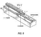
図6は、図2と同じ視点における、装置20の実際の実装である。上述のコンポーネントは、トップカバー100および支持平面102を含む支持部に搭載されている。ホルダ104、106、108、110、112のそれぞれは、フォルディングミラー42、48、フィルタ52、54、およびバウンスミラー62を、相互配列(mutual alignment)において保持している。各ホルダは、支持部に固定するように搭載された配置ポストを受容するための、複数の配置スロットを有している。このようにして、ミラーおよびフィルタが、正確に配置される。示されているように、3つのポストが存在しており、これらによって、2つの角度調整と、1つの横方向の調整とが可能である。各ホルダは、その最終的な位置に接着され得る。
FIG. 6 is an actual implementation of the
画像は、1つ以上のスキャンラインにおける画素の選択的な照明によって構成される。図7を参照して以下に詳細に記載されるように、コントローラ114は、3つのレーザビームによって、ラスターパターンにおける選択された画素を照明させ、可視状態にする。例えば、赤色、青色、および緑色の電力コントローラ116、118、120のそれぞれは、赤色、青色、および緑色のレーザ22、28、34に電流を伝導し、これらのレーザを活性化し、選択された各画素においてそれぞれの光ビームを放出すること、ならびに赤色、青色、および緑色のレーザに電流を伝導せずに、これらのレーザを不活性化し、その他の選択されていない画素を照明させない。照明された画素および照明されなかった画素の結果として得られたパターンは、人間または機械によって読取り可能な情報またはグラフィックに関する任意の表示であり得る画像を含んでいる。
The image is constructed by selective illumination of pixels in one or more scan lines. As described in detail below with reference to FIG. 7, the
図1を参照すると、ラスターパターンが、拡大図で示されている。レーザビームは、ある端点から開始して、慣性駆動部によって、水平方向に沿って、所定の水平スキャンレートで、反対の端点まで掃引され、スキャンラインを形成する。その後、レーザビームは、電磁駆動部70によって、垂直方向に沿って、所定の垂直スキャンレートで、別の端点まで掃引され、第2のスキャンラインを形成する。その後のスキャンラインの形成は、同じ方法で行われる。
Referring to FIG. 1, the raster pattern is shown in an enlarged view. The laser beam starts from one end point and is swept by the inertial drive unit along the horizontal direction at a predetermined horizontal scan rate to the opposite end point to form a scan line. Thereafter, the laser beam is swept up to another end point along the vertical direction at a predetermined vertical scan rate by the
マイクロプロセッサ114または制御回路の制御のもとで、電力コントローラ116、118、120の動作によって、レーザを変調するか、またはレーザを選択された回数だけオンおよびオフにパルス発振することにより、ラスターパターンにおいて画像が形成される。所望の画像における画素が可視であることが所望されるときにのみ、レーザは、可視光を生成し、オンにされる。各画素の色は、ビームの1つ以上の色によって決定される。可視光のスペクトルにおける任意の色は、赤色、青色、および緑色のレーザのうちの1つ以上を選択的に重ね合わせることにより、形成され得る。ラスターパターンは、各ライン上の複数の画素および複数のラインから構成された格子である。画像は、選択された画素のビットマップである。全ての文字または数字、任意のグラフィカルデザインまたはロゴ、および機械読取り可能なバーコード記号さえも、ビットマップ画像として形成され得る。
Under the control of the
図7に示されているように、入ってくるビデオ信号は、垂直および水平の同期化データならびに画素およびクロックのデータを有しており、マイクロプロセッサ114の制御のもとで、赤色、青色、および緑色のバッファ122、124、126に送信される。1つのフルVGAフレームの格納は、多くのキロバイトを必要とし、1つのフレームが書き込まれている間に、別のフレームが処理および投影されることを可能にするために、バッファにおいて、2つのフルフレームのための十分なメモリを有していることが望ましい。バッファされたデータは、スピードプロファイラ130の制御のもとで、フォーマッタ128、ならびに赤色、青色、および緑色のルックアップテーブル(LUT)132、134、136に送信され、スキャニングによって引き起こされた固有の内部歪み、ならびに投影された画像の表示角度によって引き起こされた幾何学的歪みを補正する。結果として得られた赤色、青色、および緑色のデジタル信号は、デジタルアナログ変換器(DAC)138、140、142によって、赤色、青色、および緑色のアナログ信号に変換される。赤色および青色のアナログ信号は、赤色および青色のレーザドライバ(LD)144、146に供給され、これらはまた、赤色および青色の電力コントローラ116、118にも接続されている。緑色アナログ信号は、音響光学変調器(AOM)無線周波数(RF)ドライバ150に、そして緑色レーザ34に供給され、これはまた、緑色LD148に、そして緑色電力コントローラ120にも接続されている。
As shown in FIG. 7, the incoming video signal has vertical and horizontal synchronization data and pixel and clock data, and under the control of the
フィードバック制御もまた、図7に示されており、赤色、青色、および緑色のアナログデジタル(A/D)変換器158、160、162、そしてマイクロコントローラ114に接続された、赤色、青色、および緑色のフォトダイオード増幅器152、154、156を含んでいる。A/D変換器166、そしてマイクロプロセッサに接続されたサーミスタ増幅器164によって、熱がモニタされる。
The feedback control is also shown in FIG. 7 and is red, blue, and green connected to red, blue, and green analog-to-digital (A / D)
スキャンミラー64、68は、ドライバ168、170によって駆動され、これらには、DAC172、174からのアナログ駆動信号が供給される。これらのDAC172、174は、マイクロコントローラに接続されている。フィードバック増幅器176、178は、スキャンミラー64、68の位置を検出し、フィードバックA/D180、182、そしてマイクロプロセッサに接続されている。
The scan mirrors 64 and 68 are driven by
電力管理回路184は、電力を最小化する一方で、好適には、緑色レーザを常にオンに維持し、赤色および青色のレーザの電流をレージング閾値未満に維持することによって、高速オンタイム(fast on−times)を可能にするように、動作可能である。
The
レーザ安全停止回路186は、スキャンミラー64、68のいずれか一方が、適切な位置から外れていることが検出された場合に、レーザをオフにするように動作可能である。
The laser
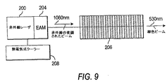
上述のように、赤外線ダイオード励起YAG結晶レーザおよび非線形周波数倍増結晶を有する緑色モジュール34、ならびに電気光学変調器36は、画像投影装置20のサイズ、重量、コスト、および電力消費の約半分を占めている。図9は、代替的な緑色レーザシステムを概略的に示しており、この緑色レーザシステムは、サイズ、重量、および電力消費を低減させ、装置20を、例えば機器10のようなハンドヘルドアプリケーションに対してより適したものとする。図8は、図9のシステムの詳細を示している。
As described above, the
代替的な緑色レーザシステムは、約1060nmの波長を有する赤外線ビームを放出するための、赤外線レーザ200を含んでいる。レーザ200は、好適には、波長安定型(wavelength stabilized)のエッジ放出レーザダイオードであり、これは、図8に示されているように、半導体チップまたは基板202上の導波体を用いて製造された分布帰還型(DFB)レーザである。レーザ200はまた、分布Bragg反射器(DBR)レーザでもあり得る。
An alternative green laser system includes an
電界吸収変調器(EAM)204は、レーザダイオード200によって放出される赤外線ビームの強度が、Frantz−Keldysh効果に基づいて、電圧を介して制御されることを可能にする半導体である。EAM204は、電極を有する変調器の導波体を含んでおり、この電極は、そこからの光学的な伝送を制御するために、変調された赤外線ビームに垂直な方向に、電場を印加する。AOM36と比較すると、EAM204は、遥かに低い電圧で動作し、遥かに低い電力を必要とし、非常に高い変調スピードで動作する。数十ギガヘルツの変調帯域幅が達成され得る。
The electroabsorption modulator (EAM) 204 is a semiconductor that allows the intensity of the infrared beam emitted by the
都合の良いことに、EAM204は、同じチップ202上で、DFBレーザダイオードと統合される。EAMは、分離したチップであり得るが、そのような統合は、EAMバンドギャップに対するレーザ波長の良好なマッチングを可能にし、別個のチップの間の整列の必要性を排除する。図8に示されているようなテーパは、レーザダイオードによって放出された赤外線ビームを、下部のEAM導波体と結合させる。
Conveniently,
EAM204によって出力された変調されたビームは、第2次高調波生成器(SHG)結晶に結合され、このSHGは、バルクデバイス(例えば、KTP)、または図9に示されているような導波体206であり得る。導波体は、その高い変換効率のために好適であり、好適には、長い周期分極反転されたニオブ酸リチウム(PPLN)の導波体が、約1060nmの波長を有している、入って来る変調された赤外線ビームを、約530nmの波長を有している、出て行く変調された緑色ビームに変換するために使用される。
The modulated beam output by the
赤外線ビームの波長の安定性を維持するために、熱電気式のクーラー208が使用され、レーザ200を一定の温度に維持する。同様に、SHG導波体206の温度を安定させることも必要であり得る。
In order to maintain the wavelength stability of the infrared beam, a
赤外線から緑色ビームへの変換は、赤外線レーザビームの出力電力の強度の2乗に比例し、EAMによって実行される変調は、緑色レーザ出力の線形のバリエーションが所望される場合に、較正され得る。 The conversion from infrared to green beam is proportional to the square of the intensity of the output power of the infrared laser beam, and the modulation performed by the EAM can be calibrated if a linear variation of the green laser output is desired.
新規であって、特許証によって保護されることが望まれるものとして請求されている内容は、添付の請求の範囲に述べられている。 What is claimed as new and desired to be protected by Letters Patent is set forth in the appended claims.
Claims (17)
a)支持部と、
b)該支持部上のレーザアセンブリであって、様々な波長の複数のレーザビームから構成される合成ビームを放出するための、レーザアセンブリと、
c)該支持部から作動距離にある空間内においてスキャンラインのパターンとして該合成ビームを掃引するための、該支持部上のスキャナであって、各スキャンラインは、多数の画素を有している、スキャナと、
d)該レーザアセンブリおよび該スキャナに動作可能なように接続されたコントローラであって、レーザビームによって、選択された画素を照明させ、可視状態にし、該画像を生成するための、コントローラと
を備えており、
e)該レーザアセンブリは、ある波長を有する赤外線ビームを放出するためのエッジ放出レーザダイオード、該赤外線ビームを変調するための電界吸収変調器、および該赤外線の変調されたビームの波長を半分にし、該複数のレーザビームのうちの1つとして緑色レーザビームを生成するための、第2次高調波生成器を含んでいる、画像投影装置。 An image projection apparatus for projecting a two-dimensional color image,
a) a support;
b) a laser assembly on the support for emitting a combined beam composed of a plurality of laser beams of various wavelengths;
c) a scanner on the support for sweeping the combined beam as a scanline pattern in a space at a working distance from the support, each scanline having a number of pixels , The scanner,
d) a controller operably connected to the laser assembly and the scanner for illuminating selected pixels with a laser beam, making them visible, and generating the image; And
e) the laser assembly includes an edge emitting laser diode for emitting an infrared beam having a wavelength, an electroabsorption modulator for modulating the infrared beam, and halving the wavelength of the infrared modulated beam; An image projection apparatus including a second harmonic generator for generating a green laser beam as one of the plurality of laser beams.
a)様々な波長の複数のレーザビームから構成される合成ビームを放出するステップと、
b)空間内においてスキャンラインのパターンとして該合成ビームを掃引するステップであって、各スキャンラインは、多数の画素を有している、ステップと、
c)該レーザビームによって、選択された画素を照明させ、可視状態にし、該画像を生成するステップと
を包含し、
d)該放出するステップは、ある波長を有する赤外線ビームを電界吸収変調することによって、そして該赤外線ビームの波長を半分にし、該複数のレーザビームのうちの1つとして緑色レーザビームを生成することによって実行される、方法。 A method for projecting a two-dimensional color image at a variable distance, comprising:
a) emitting a combined beam composed of a plurality of laser beams of various wavelengths;
b) sweeping the combined beam as a pattern of scan lines in space, each scan line having a number of pixels;
c) illuminating selected pixels with the laser beam, rendering them visible, and generating the image;
d) the emitting step includes electroabsorption modulating an infrared beam having a wavelength and halving the wavelength of the infrared beam to produce a green laser beam as one of the plurality of laser beams; The method performed by.
b)電界吸収変調器であって、該赤外線ビームを変調し、変調された赤外線ビームを形成するための、電界吸収変調器と、
c)第2次高調波生成器であって、該変調された赤外線ビームの波長を半分にし、約530ナノメートルの波長を有している緑色レーザビームを生成するための、第2次高調波生成器と
を備えている、電界吸収変調型の緑色レーザシステム。 a) an edge emitting laser diode for emitting infrared radiation having a wavelength of about 1060 nanometers;
b) an electroabsorption modulator, which modulates the infrared beam to form a modulated infrared beam;
c) a second harmonic generator for halving the wavelength of the modulated infrared beam and generating a green laser beam having a wavelength of about 530 nanometers. An electro-absorption modulation type green laser system comprising: a generator.
Applications Claiming Priority (2)
| Application Number | Priority Date | Filing Date | Title |
|---|---|---|---|
| US11/237,389 US20070070309A1 (en) | 2005-09-28 | 2005-09-28 | Color image projection arrangement and method employing electro-absorption modulated green laser system |
| PCT/US2006/034014 WO2007037908A2 (en) | 2005-09-28 | 2006-08-31 | Color image projection arrangement and method employing electro-absorption modulated green laser system |
Publications (2)
| Publication Number | Publication Date |
|---|---|
| JP2009510518A true JP2009510518A (en) | 2009-03-12 |
| JP2009510518A5 JP2009510518A5 (en) | 2009-10-15 |
Family
ID=37893412
Family Applications (1)
| Application Number | Title | Priority Date | Filing Date |
|---|---|---|---|
| JP2008533367A Withdrawn JP2009510518A (en) | 2005-09-28 | 2006-08-31 | Color image projection apparatus and method using electroabsorption modulation type green laser system |
Country Status (5)
| Country | Link |
|---|---|
| US (1) | US20070070309A1 (en) |
| JP (1) | JP2009510518A (en) |
| CN (1) | CN101297240B (en) |
| DE (1) | DE112006002607T5 (en) |
| WO (1) | WO2007037908A2 (en) |
Cited By (4)
| Publication number | Priority date | Publication date | Assignee | Title |
|---|---|---|---|---|
| JP4817274B1 (en) * | 2011-01-18 | 2011-11-16 | パナソニック株式会社 | Image display device |
| JP2012047951A (en) * | 2010-08-26 | 2012-03-08 | Seiko Epson Corp | Projector |
| JP2015064611A (en) * | 2014-12-25 | 2015-04-09 | セイコーエプソン株式会社 | Projector |
| JP2016106265A (en) * | 2016-02-17 | 2016-06-16 | セイコーエプソン株式会社 | projector |
Families Citing this family (8)
| Publication number | Priority date | Publication date | Assignee | Title |
|---|---|---|---|---|
| US9001028B2 (en) * | 2006-08-19 | 2015-04-07 | David James Baker | Projector pen |
| US7711018B2 (en) * | 2007-12-21 | 2010-05-04 | Microvision, Inc. | Method and apparatus for laser diode compensation |
| US8346028B2 (en) * | 2009-12-15 | 2013-01-01 | Kotura, Inc. | Optical device having modulator employing horizontal electrical field |
| US8585206B2 (en) * | 2010-06-29 | 2013-11-19 | Corning Incorporated | Methods for operating scanning laser projectors to reduce speckle and image flicker |
| JP5803184B2 (en) * | 2010-11-19 | 2015-11-04 | 株式会社リコー | Image projection apparatus and memory access method |
| US11104020B2 (en) | 2016-03-04 | 2021-08-31 | Harry's, Inc. | Razor handle and method of manufacture |
| CN106330329B (en) * | 2016-08-22 | 2018-07-03 | 浙江大学 | Based on the wireless light communication devices and methods therefor for directly modulating DPSSL |
| DE102021201550A1 (en) * | 2021-02-18 | 2022-08-18 | Psa Automobiles Sa | Method for operating a high-resolution projection headlight and projection headlight system for a motor vehicle |
Family Cites Families (12)
| Publication number | Priority date | Publication date | Assignee | Title |
|---|---|---|---|---|
| FI82326C (en) * | 1986-12-05 | 1991-02-11 | Lasermatic Oy | laser Head |
| US4802182A (en) * | 1987-11-05 | 1989-01-31 | Xerox Corporation | Monolithic two dimensional waveguide coupled cavity laser/modulator |
| US5206629A (en) * | 1989-02-27 | 1993-04-27 | Texas Instruments Incorporated | Spatial light modulator and memory for digitized video display |
| US5185752A (en) * | 1992-02-18 | 1993-02-09 | Spectra Diode Laboratories, Inc. | Coupling arrangements for frequency-doubled diode lasers |
| US6832724B2 (en) | 1993-03-26 | 2004-12-21 | Symbol Technologies, Inc. | Electro-optical assembly for image projection, especially in portable instruments |
| FR2724050B1 (en) * | 1994-08-31 | 1997-01-10 | Alcatel Nv | METHOD FOR ALIGNING AN UNDERGROUND TAPE AND AN EXTERNAL TAPE IN A SEMICONDUCTOR OPTICAL COMPONENT |
| JP3386261B2 (en) * | 1994-12-05 | 2003-03-17 | 三菱電機株式会社 | Optical semiconductor device and method of manufacturing the same |
| US5889913A (en) * | 1995-03-15 | 1999-03-30 | Kabushiki Kaisha Toshiba | Optical semiconductor device and method of fabricating the same |
| JPH10335751A (en) * | 1997-06-03 | 1998-12-18 | Mitsubishi Electric Corp | Semiconductor laser and its manufacture |
| US6246709B1 (en) * | 1998-06-01 | 2001-06-12 | Oki Electric Industry Co., Ltd. | Integrated optical element and method for manufacturing an integrated optical element |
| US6483863B2 (en) * | 2001-01-19 | 2002-11-19 | The Trustees Of Princeton University | Asymmetric waveguide electroabsorption-modulated laser |
| EP1372228B1 (en) * | 2002-06-12 | 2006-10-04 | Agilent Technologies, Inc. - a Delaware corporation - | Integrated semiconductor laser and waveguide device |
-
2005
- 2005-09-28 US US11/237,389 patent/US20070070309A1/en not_active Abandoned
-
2006
- 2006-08-31 JP JP2008533367A patent/JP2009510518A/en not_active Withdrawn
- 2006-08-31 DE DE112006002607T patent/DE112006002607T5/en not_active Withdrawn
- 2006-08-31 CN CN2006800398807A patent/CN101297240B/en not_active Expired - Fee Related
- 2006-08-31 WO PCT/US2006/034014 patent/WO2007037908A2/en active Application Filing
Cited By (5)
| Publication number | Priority date | Publication date | Assignee | Title |
|---|---|---|---|---|
| JP2012047951A (en) * | 2010-08-26 | 2012-03-08 | Seiko Epson Corp | Projector |
| US9063403B2 (en) | 2010-08-26 | 2015-06-23 | Seiko Epson Corporation | Projector having fluorescent body and associated sensor |
| JP4817274B1 (en) * | 2011-01-18 | 2011-11-16 | パナソニック株式会社 | Image display device |
| JP2015064611A (en) * | 2014-12-25 | 2015-04-09 | セイコーエプソン株式会社 | Projector |
| JP2016106265A (en) * | 2016-02-17 | 2016-06-16 | セイコーエプソン株式会社 | projector |
Also Published As
| Publication number | Publication date |
|---|---|
| WO2007037908A3 (en) | 2007-11-22 |
| WO2007037908A2 (en) | 2007-04-05 |
| US20070070309A1 (en) | 2007-03-29 |
| DE112006002607T5 (en) | 2008-08-21 |
| CN101297240B (en) | 2010-05-19 |
| CN101297240A (en) | 2008-10-29 |
Similar Documents
| Publication | Publication Date | Title |
|---|---|---|
| US7367682B2 (en) | Color image projection arrangement and method | |
| JP5213251B2 (en) | Correction for image distortion in image projectors | |
| JP2009510518A (en) | Color image projection apparatus and method using electroabsorption modulation type green laser system | |
| US7859600B2 (en) | Arrangement for and method of projecting a level image | |
| US7352499B2 (en) | Arrangement for and method of projecting an image with pixel mapping | |
| KR101020072B1 (en) | Arrangement for and method of projecting an image with linear scan lines | |
| US7433108B2 (en) | Arrangement for and method of improving image quality, especially for image projection arrangements | |
| US7006274B1 (en) | Compact acousto-optical modulator | |
| EP2035893B1 (en) | Arrangement for and method of projecting an image with safety circuitry | |
| JP2008547056A (en) | Tension, torsional bending, and compact drive and method for scanning light using the bending | |
| JP4681045B2 (en) | Monitoring scan mirror motion in electro-optic readers and image projectors | |
| US7460287B2 (en) | Arrangement for and method of increasing pixel symmetry, especially for image projection arrangements | |
| KR20090010096A (en) | Arrangement for and method of projecting an image to be viewed over extended viewing range | |
| US20070279509A1 (en) | Arrangement for and method of projecting an image with modulated lasers | |
| US7468508B2 (en) | System for and method of projecting an image and adjusting a data frequency of a video signal during image projection | |
| US20080204541A1 (en) | Aperture stop in an image projection arrangement for preserving color fidelity over an image | |
| JP2008535021A (en) | Compact acousto-optic modulator |
Legal Events
| Date | Code | Title | Description |
|---|---|---|---|
| A521 | Written amendment |
Free format text: JAPANESE INTERMEDIATE CODE: A523 Effective date: 20090828 |
|
| A621 | Written request for application examination |
Free format text: JAPANESE INTERMEDIATE CODE: A621 Effective date: 20090828 |
|
| A072 | Dismissal of procedure [no reply to invitation to correct request for examination] |
Free format text: JAPANESE INTERMEDIATE CODE: A073 Effective date: 20110107 |
|
| A300 | Application deemed to be withdrawn because no request for examination was validly filed |
Free format text: JAPANESE INTERMEDIATE CODE: A300 Effective date: 20110201 |