JP2009258461A - Imaging optical system, exposure device, and device manufacturing method - Google Patents
Imaging optical system, exposure device, and device manufacturing method Download PDFInfo
- Publication number
- JP2009258461A JP2009258461A JP2008108474A JP2008108474A JP2009258461A JP 2009258461 A JP2009258461 A JP 2009258461A JP 2008108474 A JP2008108474 A JP 2008108474A JP 2008108474 A JP2008108474 A JP 2008108474A JP 2009258461 A JP2009258461 A JP 2009258461A
- Authority
- JP
- Japan
- Prior art keywords
- optical axis
- optical system
- imaging
- imaging optical
- reflecting
- Prior art date
- Legal status (The legal status is an assumption and is not a legal conclusion. Google has not performed a legal analysis and makes no representation as to the accuracy of the status listed.)
- Pending
Links
Images


Abstract
Description
本発明は、結像光学系、露光装置、およびデバイス製造方法に関する。さらに詳細には、本発明は、例えばEUV光を用いてミラープロジェクション方式によりマスク上の回路パターンを感光性基板上に転写する露光装置に好適な反射型の結像光学系に関するものである。 The present invention relates to an imaging optical system, an exposure apparatus, and a device manufacturing method. More specifically, the present invention relates to a reflective imaging optical system suitable for an exposure apparatus that transfers a circuit pattern on a mask onto a photosensitive substrate by using, for example, EUV light by a mirror projection method.
従来、半導体素子などの製造に使用される露光装置として、5〜50nm程度の波長を有するEUV(Extreme UltraViolet:極紫外線)光を用いる露光装置が注目されている。露光光としてEUV光を用いる場合、使用可能な透過光学材料および屈折光学材料がないため、反射型のマスクを用いるとともに、投影光学系として反射型の結像光学系を用いることになる。 2. Description of the Related Art Conventionally, an exposure apparatus using EUV (Extreme UltraViolet) light having a wavelength of about 5 to 50 nm has attracted attention as an exposure apparatus used for manufacturing semiconductor elements. When EUV light is used as the exposure light, there is no transmissive optical material and refractive optical material that can be used, so a reflective mask is used and a reflective imaging optical system is used as the projection optical system.
従来、露光光としてEUV光を用いる露光装置に適用可能な結像光学系として、複数の反射鏡からなる反射型の光学系が提案されている(例えば特許文献1を参照)。 Conventionally, as an imaging optical system applicable to an exposure apparatus using EUV light as exposure light, a reflection type optical system composed of a plurality of reflecting mirrors has been proposed (see, for example, Patent Document 1).
露光装置では、微細なパターンを感光性基板に忠実に転写するために、波面収差ができるだけ小さいこと、すなわち結像する波面が限りなく球面に近いことが要求される。特許文献1に開示された結像光学系では、偶数次の非球面係数Cn(n=2,4,6,・・・)に加えて3次以上の奇数次の非球面係数Cn(n=3,5,7,・・・)を導入することにより、波面収差が比較的良好に補正されている。しかしながら、例えばEUV光を用いる露光装置では、波面収差をさらに小さく抑えた高性能な結像光学系が求められている。
In the exposure apparatus, in order to faithfully transfer a fine pattern onto the photosensitive substrate, it is required that the wavefront aberration is as small as possible, that is, the wavefront to be imaged is as close to a spherical surface as possible. In the imaging optical system disclosed in
本発明は、前述の課題に鑑みてなされたものであり、例えばEUV光を用いる露光装置に適用可能で、波面収差が良好に補正された高性能な結像光学系を提供することを目的とする。また、本発明の結像光学系を露光装置に適用することにより、例えば露光光としてEUV光を用いて大きな解像力を確保し、高解像度で投影露光を行うことのできる露光装置を提供することを目的とする。 The present invention has been made in view of the above-described problems, and an object thereof is to provide a high-performance imaging optical system that can be applied to, for example, an exposure apparatus that uses EUV light and that has well-corrected wavefront aberration. To do. Further, by applying the imaging optical system of the present invention to an exposure apparatus, for example, an exposure apparatus capable of ensuring a large resolving power using EUV light as exposure light and performing projection exposure with high resolution is provided. Objective.
前記課題を解決するために、本発明の第1形態では、第1面において光軸から離れた領域の像を第2面において前記光軸から離れた領域に形成する結像光学系において、
前記光軸に関して回転対称な複数の規定面によってそれぞれ規定される複数の光学面を備え、
前記複数の規定面のうちの少なくとも1つの特定規定面は、前記光軸の位置において面の傾きの変化が不連続であることを特徴とする結像光学系を提供する。
In order to solve the above-described problem, in the first aspect of the present invention, in the imaging optical system for forming an image of a region away from the optical axis on the first surface in a region away from the optical axis on the second surface,
A plurality of optical surfaces respectively defined by a plurality of rotational surfaces that are rotationally symmetric with respect to the optical axis;
At least one specific defining surface of the plurality of defining surfaces provides an imaging optical system characterized in that the change in the inclination of the surface is discontinuous at the position of the optical axis.
本発明の第2形態では、前記第1面に設置された所定のパターンを照明するための照明系と、前記所定のパターンを前記第2面に設置された感光性基板に投影するための第1形態の結像光学系とを備えていることを特徴とする露光装置を提供する。 In a second aspect of the present invention, an illumination system for illuminating a predetermined pattern installed on the first surface and a first for projecting the predetermined pattern onto a photosensitive substrate installed on the second surface. There is provided an exposure apparatus comprising an imaging optical system of one form.
本発明の第3形態では、第2形態の露光装置を用いて、前記所定のパターンを前記感光性基板に露光する露光工程と、
前記所定のパターンが転写された前記感光性基板を現像し、前記所定のパターンに対応する形状のマスク層を前記感光性基板の表面に形成する現像工程と、
前記マスク層を介して前記感光性基板の表面を加工する加工工程とを含むことを特徴とするデバイス製造方法を提供する。
In the third embodiment of the present invention, using the exposure apparatus of the second embodiment, an exposure step of exposing the predetermined pattern to the photosensitive substrate;
Developing the photosensitive substrate to which the predetermined pattern is transferred, and forming a mask layer having a shape corresponding to the predetermined pattern on the surface of the photosensitive substrate;
And a processing step of processing the surface of the photosensitive substrate through the mask layer.
本発明では、例えばEUV光を用いる反射型の結像光学系において、少なくとも1つの反射面、例えば光軸から離れた位置に有効領域を有する反射面を規定する規定面の光軸の位置における傾きの変化を不連続に設定している。その結果、すべての反射面を規定する回転対称面の傾きが光軸の位置において連続的に変化している従来技術に比して、収差補正の自由度を高めることができ、ひいては波面収差を良好に補正することができる。すなわち、本発明では、例えばEUV光を用いる露光装置に適用可能で、波面収差が良好に補正された高性能な結像光学系を実現することができる。 In the present invention, for example, in a reflective imaging optical system using EUV light, the inclination at the position of the optical axis of at least one reflecting surface, for example, a prescribed surface that defines a reflecting surface having an effective area at a position away from the optical axis. The change is set discontinuously. As a result, the degree of freedom of aberration correction can be increased as compared with the prior art in which the inclination of the rotationally symmetric surface that defines all reflecting surfaces continuously changes at the position of the optical axis, and thus the wavefront aberration can be reduced. It can be corrected well. In other words, the present invention can be applied to, for example, an exposure apparatus that uses EUV light, and can realize a high-performance image-forming optical system in which wavefront aberration is well corrected.
また、本発明の結像光学系を露光装置に適用することにより、露光光として例えば20nm以下の波長のEUV光を使用することができる。この場合、結像光学系に対して転写すべき所定のパターンおよび感光性基板を相対移動させて、所定のパターンを感光性基板上へ高解像度で投影露光することが可能になる。その結果、大きな解像力を有する走査型の露光装置を用いて、良好な露光条件のもとで、高精度なデバイスを製造することができる。 Further, by applying the imaging optical system of the present invention to an exposure apparatus, EUV light having a wavelength of, for example, 20 nm or less can be used as exposure light. In this case, the predetermined pattern to be transferred and the photosensitive substrate are moved relative to the imaging optical system, and the predetermined pattern can be projected and exposed onto the photosensitive substrate with high resolution. As a result, a highly accurate device can be manufactured under good exposure conditions using a scanning exposure apparatus having a large resolving power.
一般に、EUV光を用いる露光装置に適用可能な結像光学系は、光軸に関して回転対称な面によってそれぞれ規定される複数の反射面を有し、物体面(第1面)において光軸から離れた領域の像を像面(第2面)において光軸から離れた領域に形成する。従来、この種の結像光学系では、すべての反射面を規定する回転対称面(以下、「規定面」という)の傾きが光軸の位置において連続的に変化していた。 In general, an imaging optical system applicable to an exposure apparatus using EUV light has a plurality of reflecting surfaces respectively defined by rotationally symmetric surfaces with respect to the optical axis, and is separated from the optical axis on the object surface (first surface). An image of the region is formed in a region away from the optical axis on the image plane (second surface). Conventionally, in this type of imaging optical system, the inclination of a rotationally symmetric surface that defines all reflecting surfaces (hereinafter referred to as a “specified surface”) continuously changes at the position of the optical axis.
本発明者らは、例えばEUV光を用いる露光装置に適用可能な反射型の結像光学系では、少なくとも1つの反射面が光軸から離れた位置に有効領域(有効な結像光束が入射する領域)を有することに着目し、例えば光軸から離れた位置に有効領域を有する反射面を規定する規定面の光軸の位置における傾きの変化をあえて不連続に設定することにより、収差補正の自由度を高めること、ひいては波面収差をさらに良好に補正することを試みた。 For example, in a reflective imaging optical system applicable to an exposure apparatus that uses EUV light, the present inventors have provided an effective region (effective imaging light beam is incident at a position where at least one reflecting surface is separated from the optical axis. For example, by setting the change in inclination at the position of the optical axis of the prescribed surface that defines the reflecting surface having an effective region at a position away from the optical axis to be discontinuous, An attempt was made to increase the degree of freedom, and thus to correct the wavefront aberration more satisfactorily.
本発明の実施形態を、添付図面に基づいて説明する。図1は、本発明の実施形態にかかる露光装置の構成を概略的に示す図である。また、図2は、ウェハ上に形成される円弧状の有効結像領域と光軸との位置関係を示す図である。図1において、結像光学系6の光軸AX方向すなわち感光性基板であるウェハWの露光面(転写面)の法線方向に沿ってZ軸を、ウェハWの露光面内において図1の紙面に平行な方向にY軸を、ウェハWの露光面内において図1の紙面に垂直な方向にX軸をそれぞれ設定している。
Embodiments of the present invention will be described with reference to the accompanying drawings. FIG. 1 is a drawing schematically showing a configuration of an exposure apparatus according to an embodiment of the present invention. FIG. 2 is a diagram showing the positional relationship between the arc-shaped effective imaging region formed on the wafer and the optical axis. In FIG. 1, the Z axis along the optical axis AX direction of the imaging
図1の露光装置は、露光光を供給するための光源として、たとえばレーザプラズマX線源1を備えている。なお、X線源として、放電プラズマ光源や他のX線源を用いることが可能である。X線源1から射出された光は、波長選択フィルタ2を介して、照明光学系3に入射する。波長選択フィルタ2は、X線源1が供給する光から、所定波長(例えば13.5nm)のEUV光だけを選択的に透過させ、他の波長光の透過を遮る特性を有する。
The exposure apparatus shown in FIG. 1 includes, for example, a laser
波長選択フィルタ2を透過したEUV光は、複数の反射鏡から構成された照明光学系3を介して、転写すべきパターンが形成された反射型のマスク4を照明する。なお、波長選択フィルタ2の配置は必須ではなく、反射鏡に形成された波長選択膜を用いてもよいし、他の形態の波長選択手段を用いてもよい。また、波長選択フィルタ2及び他の波長選択手段そのものを配置しなくてもよい。
The EUV light transmitted through the
マスク4は、そのパターン面がXY平面に沿って延びるように、Y方向に沿って移動可能なマスクステージ5によって保持されている。そして、マスクステージ5の移動は、図示を省略したレーザー干渉計により計測されるように構成されている。マスク4上には、Y軸に関して対称な円弧状の照明領域が形成される。照明されたマスク4からの光は、反射型の結像光学系6を介して、感光性基板であるウェハ7上にマスクパターンの像を形成する。
The
すなわち、ウェハ7上には、図2に示すように、Y軸に関して対称な円弧状の有効結像領域が形成される。図2を参照すると、光軸AXを中心とした半径Y0を有する円形状の領域(イメージサークル)IF内において、このイメージサークルIFに接するようにX方向の長さがLXでY方向の長さがLYの円弧状の有効結像領域ERが設定されている。円弧状の有効結像領域ERは光軸AXを中心とする輪帯状の領域の一部であり、長さLYは円弧状の有効結像領域ERの中心と光軸とを結ぶ方向に沿った有効結像領域ERの幅寸法である。
That is, on the
ウェハ7は、その露光面がXY平面に沿って延びるように、X方向およびY方向に沿って二次元的に移動可能なウェハステージ8によって保持されている。なお、ウェハステージ8の移動は、マスクステージ5と同様に、図示を省略したレーザー干渉計により計測されるように構成されている。こうして、マスクステージ5およびウェハステージ8をY方向に沿って移動させながら、すなわち投影光学系としての結像光学系6に対してマスク4およびウェハ7をY方向に沿って相対移動させながらスキャン露光(走査露光)を行うことにより、ウェハ7の1つの露光領域にマスク4のパターンが転写される。
The
このとき、結像光学系6の投影倍率(転写倍率)が1/4である場合、ウェハステージ8の移動速度をマスクステージ5の移動速度の1/4に設定して同期走査を行う。また、ウェハステージ8をX方向およびY方向に沿って二次元的に移動させながら走査露光を繰り返すことにより、ウェハ7の各露光領域にマスク4のパターンが逐次転写される。以下、比較例および第1乃至第6実施例を参照して、結像光学系の具体的な構成について説明する。
At this time, when the projection magnification (transfer magnification) of the imaging
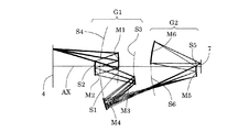
比較例および各実施例の結像光学系は、図3に示すように、直線状に延びる単一の光軸AXに沿って、マスク4のパターン面と共役な位置にパターンの中間像を形成するための第1反射光学系G1と、マスク4のパターンの最終縮小像(中間像の像)をウェハ7上に形成するための第2反射光学系G2とにより構成されている。すなわち、マスク4のパターン面と光学的に共役な面が、第1反射光学系G1と第2反射光学系G2との間の光路中に形成される。
As shown in FIG. 3, the imaging optical system of the comparative example and each example forms an intermediate image of the pattern at a position conjugate with the pattern surface of the
第1反射光学系G1は、光の入射順に、凹面状の反射面を有する第1反射鏡M1と、凹面状の反射面を有する第2反射鏡M2と、凸面状の反射面を有する第3反射鏡M3と、凹面状の反射面を有する第4反射鏡M4とにより構成されている。第2反射光学系G2は、光の入射順に、凸面状の反射面を有する第5反射鏡M5と、凹面状の反射面を有する第6反射鏡M6とにより構成されている。第2反射鏡M2の反射面の位置に、開口絞り(不図示)が設けられている。 The first reflecting optical system G1 has a first reflecting mirror M1 having a concave reflecting surface, a second reflecting mirror M2 having a concave reflecting surface, and a third reflecting surface having a convex reflecting surface in the light incident order. The reflecting mirror M3 is configured by a fourth reflecting mirror M4 having a concave reflecting surface. The second reflecting optical system G2 is configured by a fifth reflecting mirror M5 having a convex reflecting surface and a sixth reflecting mirror M6 having a concave reflecting surface in the light incident order. An aperture stop (not shown) is provided at the position of the reflecting surface of the second reflecting mirror M2.
比較例および各実施例では、マスク4のパターン面(第1面)において光軸AXから離れた領域(照明領域)からの光が、第1反射鏡M1の凹面状の反射面、第2反射鏡M2の凹面状の反射面、第3反射鏡M3の凸面状の反射面、および第4反射鏡M4の凹面状の反射面で順次反射された後、マスクパターンの中間像を形成する。第1反射光学系G1を介して形成された中間像からの光は、第5反射鏡M5の凸面状の反射面および第6反射鏡M6の凹面状の反射面で順次反射された後、ウェハ7の表面(第2面)において光軸AXから離れた領域(有効結像領域ER)にマスクパターンの縮小像(二次像)を形成する。
In the comparative example and each example, the light from the region (illumination region) away from the optical axis AX on the pattern surface (first surface) of the
比較例および各実施例において、すべての反射鏡M1〜M6の反射面は、光軸AXに関して回転対称な非球面状の規定面S1〜S6によって規定されている。ここで、第3反射鏡M3、第4反射鏡M4、および第6反射鏡M6の反射面は、光軸AXから離れた位置に有効領域を有する。第1反射鏡M1および第5反射鏡M5の反射面では、有効領域の周縁付近において光軸AXと交差している。第2反射鏡M2の反射面では、有効領域の中央付近において光軸AXと交差している。 In the comparative example and each example, the reflecting surfaces of all the reflecting mirrors M1 to M6 are defined by aspherical defining surfaces S1 to S6 that are rotationally symmetric with respect to the optical axis AX. Here, the reflecting surfaces of the third reflecting mirror M3, the fourth reflecting mirror M4, and the sixth reflecting mirror M6 have an effective area at a position away from the optical axis AX. The reflecting surfaces of the first reflecting mirror M1 and the fifth reflecting mirror M5 intersect the optical axis AX near the periphery of the effective area. The reflecting surface of the second reflecting mirror M2 intersects the optical axis AX near the center of the effective area.
また、比較例および各実施例の結像光学系は、ウェハ側(像側)にほぼテレセントリックな光学系である。換言すれば、比較例および各実施例において、結像光学系の像面上の各位置に達する主光線は像面に対してほぼ垂直である。この構成により、結像光学系の焦点深度内でウェハに凹凸があっても良好な結像が可能になっている。 Further, the imaging optical systems of the comparative example and each example are optical systems that are almost telecentric on the wafer side (image side). In other words, in the comparative example and each example, the principal ray reaching each position on the image plane of the imaging optical system is substantially perpendicular to the image plane. With this configuration, good image formation is possible even if the wafer has irregularities within the depth of focus of the imaging optical system.
比較例および各実施例において、反射鏡M1〜M6の反射面を規定する規定面S1〜S6は、光軸AXに垂直な方向の高さをyとし、当該規定面と光軸AXとの交点を含み且つ光軸AXに垂直な面から高さyにおける当該規定面上の位置までの光軸AXに沿った距離(サグ量)をzとし、光軸AXにおける当該規定面の中心曲率半径をrとし、円錐係数(コーニック定数)をκとし、n(nは28以下の正の整数)次の非球面係数をCnとし、Σをnに関する総和記号としたとき、以下の式(a)で表される。ただし、比較例および各実施例において、2次の非球面係数C2、および3次以上の奇数次の非球面係数(C3,C5,C7,・・・,C27)は、0である。 In the comparative example and each example, the defining surfaces S1 to S6 that define the reflecting surfaces of the reflecting mirrors M1 to M6 have a height in the direction perpendicular to the optical axis AX as y, and the intersection between the defining surface and the optical axis AX. The distance (sag amount) along the optical axis AX from the plane perpendicular to the optical axis AX to the position on the defined plane at the height y is z, and the center curvature radius of the defined plane on the optical axis AX is When r is a cone coefficient (conic constant) κ, n (n is a positive integer equal to or less than 28) aspherical coefficient C n, and Σ is a summation symbol for n, the following equation (a) It is represented by However, in the comparative example and each example, the second-order aspheric coefficient C 2 and the third-order or higher-order aspheric coefficient (C 3 , C 5 , C 7 ,..., C 27 ) are 0 It is.
z=(y2/r)/{1+{1−(1+κ)・y2/r2}1/2}+ΣCn・yn (a) z = (y 2 / r) / {1+ {1− (1 + κ) · y 2 / r 2 } 1/2 } + ΣC n · y n (a)
[比較例]
各実施例の効果を検証するための比較例として、特許文献1に開示された開口数NAが0.25の結像光学系をNA=0.33に最適化した結像光学系を用いる。比較例の結像光学系では、各反射鏡M1〜M6の反射面を規定する規定面S1〜S6が、4次以上の偶数次の非球面係数(C4,C6,C8,・・・,C28)とコーニック定数κとを用いて非球面式(a)により定義されている。換言すれば、比較例では、規定面S1〜S6を表す非球面式(a)において1次の非球面係数C1が0であり、すべての反射面を規定する回転対称面の傾きが光軸AXの位置において連続的に変化している。
[Comparative example]
As a comparative example for verifying the effect of each embodiment, an imaging optical system that is an optimization of the imaging optical system disclosed in
次の表(1)に、比較例にかかる結像光学系の諸元の値を掲げる。表(1)の主要諸元の欄において、λは露光光の波長を、βは結像倍率を、NAは像側(ウェハ側)開口数を、Y0はウェハ7上でのイメージサークルIFの半径(最大像高)を、LXは有効結像領域ERのX方向に沿った寸法を、LYは有効結像領域ERのY方向に沿った寸法(円弧状の有効結像領域ERの幅寸法)をそれぞれ表している。
The following table (1) lists the values of the specifications of the imaging optical system according to the comparative example. In the column of main specifications in Table (1), λ is the wavelength of the exposure light, β is the imaging magnification, NA is the numerical aperture on the image side (wafer side), and Y0 is the image circle IF on the
また、表(1)の光学部材諸元の欄において、面番号は物体面であるマスク面から像面であるウェハ面への光線の進行する方向に沿ったマスク側からの反射面の順序を、rは各反射面の中心曲率半径(mm)を、dは各反射面の軸上間隔すなわち次の反射面までの面間隔(mm)をそれぞれ示している。なお、面間隔dは、反射される度にその符号を変えるものとする。そして、光線の入射方向にかかわらずマスク側に向かって凸面の曲率半径を正とし、凹面の曲率半径を負としている。上述の表記は、以降の表(2)〜(7)においても同様である。また、主要諸元の値は、比較例および各実施例に共通である。 In the column of the optical member specifications in Table (1), the surface number indicates the order of the reflecting surface from the mask side along the direction in which the light beam travels from the mask surface that is the object surface to the wafer surface that is the image surface. R represents the central radius of curvature (mm) of each reflecting surface, and d represents the axial distance between each reflecting surface, that is, the surface spacing (mm) to the next reflecting surface. Note that the surface distance d changes its sign each time it is reflected. The curvature radius of the convex surface toward the mask side is positive and the curvature radius of the concave surface is negative regardless of the incident direction of the light beam. The above notation is the same in the following tables (2) to (7). Moreover, the value of main specifications is common to a comparative example and each Example.
表(1)
(主要諸元)
λ=13.5nm
β=1/4
NA=0.33
Y0=30.5mm
LX=26mm
LY=2mm
(光学部材諸元)
面番号 r d 光学部材
(マスク面) 557.6270
1 -844.8251 -193.7591 (第1反射鏡M1)
2 1849.6608 324.4344 (第2反射鏡M2)
3 474.5683 -284.8868 (第3反射鏡M3)
4 572.0570 813.8823 (第4反射鏡M4)
5 283.4708 -380.1421 (第5反射鏡M5)
6 456.1063 426.0113 (第6反射鏡M6)
(ウェハ面)
(非球面データ)
1面(規定面S1)
κ=0.0335
C1=0 C4=3.2775×10⁻⁹
C6=−7.1910×10⁻¹⁴ C8=1.4747×10⁻¹⁸
C10=3.2151×10⁻²² C12=−1.2401×10⁻²⁵
C14=2.4378×10⁻²⁹ C16=−2.8472×10⁻³³
C18=1.8639×10-37 C20=−5.2552×10-42
C22=−1.9312×10-47 C24=9.2139×10-52
C26=4.8754×10-56 C28=4.5066×10-60
2面(規定面S2)
κ=−0.9960
C1=0 C4=−1.2492×10⁻⁹
C6=−1.4376×10⁻¹³ C8=2.0066×10⁻¹⁶
C10=−3.9834×10⁻¹⁹ C12=5.2058×10⁻²²
C14=−4.7306×10⁻²⁵ C16=2.9142×10⁻²⁸
C18=−1.0924×10⁻³¹ C20=1.6491×10⁻³⁵
C22=2.1723×10-39 C24=2.9531×10-43
C26=−8.5433×10-46 C28=1.7959×10-49
3面(規定面S3)
κ=0.0083
C1=0 C4=−1.8966×10⁻⁹
C6=−1.4369×10⁻¹⁴ C8=2.1691×10⁻¹⁸
C10=1.4740×10⁻²² C12=−6.7111×10⁻²⁶
C14=7.5306×10⁻³⁰ C16=−3.5355×10⁻³⁴
C18=3.8922×10-39 C20=6.0553×10-44
C22=−6.7086×10-48 C24=7.7867×10-52
C26=1.0408×10-55 C28=−7.9322×10-60
4面(規定面S4)
κ=0.0011
C1=0 C4=9.1480×10⁻¹²
C6=−1.1332×10⁻¹⁵ C8=2.1083×10⁻²⁰
C10=−1.4124×10⁻²⁵ C12=−5.0793×10⁻³¹
C14=−1.6401×10⁻³⁵ C16=7.8134×10-40
C18=−8.8014×10-45 C20=3.5847×10-50
C22=−1.6333×10-56 C24=−3.1828×10-61
C26=8.6203×10-67 C28=1.7909×10-71
5面(規定面S5)
κ=0.0027
C1=0 C4=5.4675×10⁻¹⁰
C6=1.3109×10⁻¹² C8=−8.5488×10⁻¹⁸
C10=−1.0981×10⁻¹⁹ C12=1.4049×10⁻²²
C14=−1.0619×10⁻²⁵ C16=4.8183×10⁻²⁹
C18=−1.2219×10⁻³² C20=1.3543×10-36
C22=3.9166×10-42 C24=−3.2339×10-45
C26=−4.6695×10-49 C28=−8.7682×10-53
6面(規定面S6)
κ=−0.0002
C1=0 C4=7.4684×10⁻¹¹
C6=4.4789×10⁻¹⁶ C8=8.3332×10⁻²¹
C10=−8.6772×10⁻²⁵ C12=8.8677×10⁻²⁹
C14=−5.9257×10⁻³³ C16=2.5541×10-37
C18=−6.4978×10-42 C20=7.4576×10-47
C22=1.4838×10-52 C24=−3.5904×10-57
C26=−2.0742×10-61 C28=2.5156×10-66
Table (1)
(Main specifications)
λ = 13.5nm
β = 1/4
NA = 0.33
Y0 = 30.5mm
LX = 26mm
LY = 2mm
(Optical member specifications)
Surface number rd Optical member (mask surface) 557.6270
1 -844.8251 -193.7591 (First reflector M1)
2 1849.6608 324.4344 (Second reflector M2)
3 474.5683 -284.8868 (Third reflector M3)
4 572.0570 813.8823 (4th reflector M4)
5 283.4708 -380.1421 (5th reflector M5)
6 456.1063 426.0113 (6th reflector M6)
(Wafer surface)
(Aspheric data)
1 surface (regulated surface S1)
κ = 0.0335
C 1 = 0 C 4 = 3.2775 × 10 −9
C 6 = −7.1910 × 10 −14 C 8 = 1.4747 × 10 −18
C 10 = 3.2151 × 10 −22 C 12 = −1.2401 × 10 −25
C 14 = 2.4378 × 10 −29 C 16 = −2.8472 × 10 −33
C 18 = 1.8639 × 10 −37 C 20 = −5.2552 × 10 −42
C 22 = −1.9312 × 10 −47 C 24 = 9.2139 × 10 −52
C 26 = 4.8754 × 10 −56 C 28 = 4.5066 × 10 −60
2 sides (regulated surface S2)
κ = −0.9960
C 1 = 0 C 4 = −1.2492 × 10 −9
C 6 = −1.4376 × 10 −13 C 8 = 2.0066 × 10 −16
C 10 = −3.99844 × 10 −19 C 12 = 5.2058 × 10 −22
C 14 = −4.7306 × 10 −25 C 16 = 2.9142 × 10 −28
C 18 = −1.0924 × 10 −31 C 20 = 1.6491 × 10 −35
C 22 = 2.1723 × 10 −39 C 24 = 2.99511 × 10 −43
C 26 = −8.5433 × 10 −46 C 28 = 1.7959 × 10 −49
3 sides (regulated surface S3)
κ = 0.0083
C 1 = 0 C 4 = −1.8966 × 10 −9
C 6 = −1.4369 × 10 −14 C 8 = 2.1691 × 10 −18
C 10 = 1.4740 × 10 −22 C 12 = −6.7111 × 10 −26
C 14 = 7.5306 × 10 −30 C 16 = −3.5355 × 10 −34
C 18 = 3.8922 × 10 −39 C 20 = 6.0553 × 10 −44
C 22 = −6.7068 × 10 −48 C 24 = 7.7867 × 10 −52
C 26 = 1.0408 × 10 −55 C 28 = −7.9322 × 10 −60
4 (regulated surface S4)
κ = 0.0011
C 1 = 0 C 4 = 9.1480 × 10 −12
C 6 = −1.332 × 10 −15 C 8 = 2.1083 × 10 −20
C 10 = −1.4124 × 10 −25 C 12 = −5.0793 × 10 −31
C 14 = −1.6401 × 10 −35 C 16 = 7.8134 × 10 −40
C 18 = −8.8014 × 10 −45 C 20 = 3.5847 × 10 −50
C 22 = −1.6333 × 10 −56 C 24 = −3.1828 × 10 −61
C 26 = 8.6203 × 10 −67 C 28 = 1.7909 × 10 −71
5 (regulated surface S5)
κ = 0.527
C 1 = 0 C 4 = 5.4675 × 10 −10
C 6 = 1.3109 × 10 −12 C 8 = −8.5488 × 10 −18
C 10 = −1.0981 × 10 −19 C 12 = 1.4049 × 10 −22
C 14 = −1.0619 × 10 −25 C 16 = 4.8183 × 10 −29
C 18 = −1.2219 × 10 −32 C 20 = 1.3543 × 10 −36
C 22 = 3.9166 × 10 −42 C 24 = −3.2339 × 10 −45
C 26 = −4.6695 × 10 −49 C 28 = −8.7682 × 10 −53
6 (regular surface S6)
κ = −0.0002
C 1 = 0 C 4 = 7.4684 × 10 −11
C 6 = 4.4789 × 10 −16 C 8 = 8.3332 × 10 −21
C 10 = −8.6772 × 10 −25 C 12 = 8.8877 × 10 −29
C 14 = −5.9257 × 10 −33 C 16 = 2.5541 × 10 −37
C 18 = −6.4978 × 10 −42 C 20 = 7.4576 × 10 −47
C 22 = 1.4838 × 10 −52 C 24 = −3.5904 × 10 −57
C 26 = −2.0742 × 10 −61 C 28 = 2.5156 × 10 −66
[第1実施例]
第1実施例の結像光学系は、比較例にかかる結像光学系を基に、第4反射鏡M4の反射面を規定する規定面S4を表す非球面式(a)にのみ1次の非球面係数C1を導入して最適化したものである。すなわち、第1実施例では、規定面S4以外の各規定面の傾きは光軸AXの位置において連続的に変化しているが、規定面S4の光軸AXの位置における傾きの変化は不連続である。
[First embodiment]
The imaging optical system of the first example is based on the imaging optical system according to the comparative example, and the first order only to the aspherical surface formula (a) representing the defining surface S4 that defines the reflecting surface of the fourth reflecting mirror M4. An aspherical coefficient C 1 is introduced and optimized. That is, in the first embodiment, the inclination of each prescribed surface other than the prescribed surface S4 continuously changes at the position of the optical axis AX, but the change in inclination at the position of the optical axis AX of the prescribed surface S4 is discontinuous. It is.
ちなみに、非球面式(a)において1次の非球面係数C1のみにより定義される1次の非球面は、光軸を回転対称の中心とする円錐体の側面の面形状(すなわち円錐面形状)を有する。図4に示すように、物体面OPと像面IPとを共役に結ぶ屈折型の結像光学系を構成する1つまたは複数の光学面R1に1次の非球面を適用すると、光学面R1の光軸AXの位置における傾きの変化は不連続であり、光学面R1の光軸AXを含む領域を光束が通過する。その結果、光学面R1の傾きの変化が不連続な光軸AXの位置で波面の傾きが不連続になり、光学面R1の傾きの変化の不連続性に起因して波面収差が発生する。 Incidentally, the primary aspherical surface defined by only the primary aspherical coefficient C 1 in the aspherical surface formula (a) is the surface shape of the side surface of the cone having the optical axis as the rotational symmetry center (that is, the conical surface shape). ). As shown in FIG. 4, when a primary aspheric surface is applied to one or a plurality of optical surfaces R1 constituting a refractive imaging optical system that conjugates an object plane OP and an image plane IP, the optical surface R1. The change in inclination at the position of the optical axis AX is discontinuous, and the light beam passes through the region including the optical axis AX of the optical surface R1. As a result, the inclination of the wavefront becomes discontinuous at the position of the optical axis AX where the change in the inclination of the optical surface R1 is discontinuous, and wavefront aberration occurs due to the discontinuity in the change in the inclination of the optical surface R1.
これに対し、第1実施例では、光軸AXから離れた位置に有効領域を有する第4反射鏡M4の反射面を規定する規定面S4のみにおいて、光軸AXの位置における面の傾きの変化を不連続にしている。したがって、第1実施例では、規定面S4の傾きの変化が不連続な光軸AXの領域を結像光束が通過することはない。次の表(2)に、第1実施例にかかる結像光学系の諸元の値を掲げる。 On the other hand, in the first embodiment, the change in the inclination of the surface at the position of the optical axis AX only in the defining surface S4 that defines the reflecting surface of the fourth reflecting mirror M4 having an effective area at a position away from the optical axis AX. Is discontinuous. Therefore, in the first embodiment, the imaging light flux does not pass through the region of the optical axis AX where the change in the inclination of the defining surface S4 is discontinuous. In the following table (2), values of specifications of the imaging optical system according to the first example are listed.
表(2)
(主要諸元)
λ=13.5nm
β=1/4
NA=0.33
Y0=30.5mm
LX=26mm
LY=2mm
(光学部材諸元)
面番号 r d 光学部材
(マスク面) 557.7447
1 -844.8306 -194.0636 (第1反射鏡M1)
2 1849.8189 324.4338 (第2反射鏡M2)
3 474.6183 -284.9001 (第3反射鏡M3)
4 572.0502 813.8840 (第4反射鏡M4)
5 283.4736 -380.1380 (第5反射鏡M5)
6 456.1078 426.0088 (第6反射鏡M6)
(ウェハ面)
(非球面データ)
1面(規定面S1)
κ=0.0335
C1=0 C4=3.2879×10⁻⁹
C6=−7.1771×10⁻¹⁴ C8=1.4284×10⁻¹⁸
C10=3.2579×10⁻²² C12=−1.2382×10⁻²⁵
C14=2.4349×10⁻²⁹ C16=−2.8500×10⁻³³
C18=1.8644×10-37 C20=−5.2274×10-42
C22=−1.7398×10-47 C24=8.2373×10-52
C26=2.2886×10-56 C28=5.6244×10-60
2面(規定面S2)
κ=−0.9960
C1=0 C4=−1.2441×10⁻⁹
C6=−1.3931×10⁻¹³ C8=1.9449×10⁻¹⁶
C10=−3.9603×10⁻¹⁹ C12=5.2111×10⁻²²
C14=−4.7327×10⁻²⁵ C16=2.9129×10⁻²⁸
C18=−1.0927×10⁻³¹ C20=1.6501×10⁻³⁵
C22=2.1817×10-39 C24=2.9941×10-43
C26=−8.5383×10-46 C28=1.7838×10-49
3面(規定面S3)
κ=0.0083
C1=0 C4=−1.9042×10⁻⁹
C6=−1.3899×10⁻¹⁴ C8=2.1345×10⁻¹⁸
C10=1.4643×10⁻²² C12=−6.6931×10⁻²⁶
C14=7.5432×10⁻³⁰ C16=−3.5396×10⁻³⁴
C18=3.7533×10-39 C20=5.7344×10-44
C22=−6.4857×10-48 C24=8.4891×10-52
C26=1.0570×10-55 C28=−8.2669×10-60
4面(規定面S4)
κ=0.0011
C1=−3.9741×10⁻⁵ C4=9.1714×10⁻¹²
C6=−1.1529×10⁻¹⁵ C8=2.1076×10⁻²⁰
C10=−1.4012×10⁻²⁵ C12=−4.7959×10⁻³¹
C14=−1.6376×10⁻³⁵ C16=7.7847×10-40
C18=−8.8562×10-45 C20=3.5308×10-50
C22=−1.1829×10-56 C24=−1.3643×10-61
C26=2.2714×10-66 C28=−1.2682×10-71
5面(規定面S5)
κ=0.0027
C1=0 C4=4.6836×10⁻¹⁰
C6=1.3136×10⁻¹² C8=−1.2724×10⁻¹⁷
C10=−1.0702×10⁻¹⁹ C12=1.4021×10⁻²²
C14=−1.0654×10⁻²⁵ C16=4.8172×10⁻²⁹
C18=−1.2186×10⁻³² C20=1.3724×10-36
C22=3.9166×10-42 C24=−5.9280×10-45
C26=−1.2609×10-48 C28=2.4912×10-52
6面(規定面S6)
κ=−0.0002
C1=0 C4=7.4622×10⁻¹¹
C6=4.5047×10⁻¹⁶ C8=8.0150×10⁻²¹
C10=−8.5095×10⁻²⁵ C12=8.8607×10⁻²⁹
C14=−5.9401×10⁻³³ C16=2.5526×10-37
C18=−6.4872×10-42 C20=7.5038×10-47
C22=1.5137×10-52 C24=−4.0571×10-57
C26=−2.2615×10-61 C28=3.0878×10-66
Table (2)
(Main specifications)
λ = 13.5nm
β = 1/4
NA = 0.33
Y0 = 30.5mm
LX = 26mm
LY = 2mm
(Optical member specifications)
Surface number rd Optical member (mask surface) 557.7447
1 -844.8306 -194.0636 (First reflector M1)
2 1849.8189 324.4338 (Second reflector M2)
3 474.6183 -284.9001 (3rd reflector M3)
4 572.0502 813.8840 (4th reflector M4)
5 283.4736 -380.1380 (5th reflector M5)
6 456.1078 426.0088 (6th reflector M6)
(Wafer surface)
(Aspheric data)
1 surface (regulated surface S1)
κ = 0.0335
C 1 = 0 C 4 = 3.2879 × 10 −9
C 6 = −7.1771 × 10 −14 C 8 = 1.4284 × 10 −18
C 10 = 3.2579 × 10 −22 C 12 = −1.2382 × 10 −25
C 14 = 2.4349 × 10 −29 C 16 = −2.8500 × 10 −33
C 18 = 1.8644 × 10 −37 C 20 = −5.2274 × 10 −42
C 22 = −1.7398 × 10 −47 C 24 = 8.2373 × 10 −52
C 26 = 2.2886 × 10 −56 C 28 = 5.6244 × 10 −60
2 sides (regulated surface S2)
κ = −0.9960
C 1 = 0 C 4 = −1.2441 × 10 −9
C 6 = −1.3931 × 10 −13 C 8 = 1.9449 × 10 −16
C 10 = −3.9603 × 10 −19 C 12 = 5.2111 × 10 −22
C 14 = −4.7327 × 10 −25 C 16 = 2.9129 × 10 −28
C 18 = −1.0927 × 10 −31 C 20 = 1.6501 × 10 −35
C 22 = 2.1817 × 10 −39 C 24 = 2.9941 × 10 −43
C 26 = −8.5383 × 10 −46 C 28 = 1.7838 × 10 −49
3 sides (regulated surface S3)
κ = 0.0083
C 1 = 0 C 4 = −1.9042 × 10 −9
C 6 = −1.3899 × 10 −14 C 8 = 2.1345 × 10 −18
C 10 = 1.4643 × 10 −22 C 12 = −6.6931 × 10 −26
C 14 = 7.5432 × 10 −30 C 16 = −3.5396 × 10 −34
C 18 = 3.7533 × 10 −39 C 20 = 5.7344 × 10 −44
C 22 = −6.4857 × 10 −48 C 24 = 8.4891 × 10 −52
C 26 = 1.0570 × 10 −55 C 28 = −8.2669 × 10 −60
4 (regulated surface S4)
κ = 0.0011
C 1 = -3.9741 × 10 −5 C 4 = 9.1714 × 10 −12
C 6 = −1.529 × 10 −15 C 8 = 2.1076 × 10 −20
C 10 = −1.4012 × 10 −25 C 12 = −4.7959 × 10 −31
C 14 = −1.6376 × 10 −35 C 16 = 7.7847 × 10 −40
C 18 = −8.8562 × 10 −45 C 20 = 3.5308 × 10 −50
C 22 = −1.1829 × 10 −56 C 24 = −1.3643 × 10 −61
C 26 = 2.2714 × 10 −66 C 28 = −1.2682 × 10 −71
5 (regulated surface S5)
κ = 0.527
C 1 = 0 C 4 = 4.6836 × 10 −10
C 6 = 1.3136 × 10 −12 C 8 = −1.2724 × 10 −17
C 10 = −1.0702 × 10 −19 C 12 = 1.4021 × 10 −22
C 14 = −1.0654 × 10 −25 C 16 = 4.8172 × 10 −29
C 18 = −1.2186 × 10 −32 C 20 = 1.3724 × 10 −36
C 22 = 3.9166 × 10 −42 C 24 = −5.9280 × 10 −45
C 26 = −1.2609 × 10 −48 C 28 = 2.4912 × 10 −52
6 (regular surface S6)
κ = −0.0002
C 1 = 0 C 4 = 7.4622 × 10 −11
C 6 = 4.5047 × 10 −16 C 8 = 8.0150 × 10 −21
C 10 = −8.5095 × 10 −25 C 12 = 8.8607 × 10 −29
C 14 = −5.9401 × 10 −33 C 16 = 2.5526 × 10 −37
C 18 = −6.4872 × 10 −42 C 20 = 7.5038 × 10 −47
C 22 = 1.5137 × 10 −52 C 24 = −4.0571 × 10 −57
C 26 = −2.2615 × 10 −61 C 28 = 3.0878 × 10 −66
[第2実施例]
第2実施例の結像光学系は、比較例にかかる結像光学系を基に、第1反射鏡M1および第4反射鏡M4の反射面を規定する規定面S1およびS4を表す非球面式(a)にのみ1次の非球面係数C1を導入して最適化したものである。すなわち、第2実施例では、規定面S2、S3、S5およびS6の傾きは光軸AXの位置において連続的に変化しているが、規定面S1およびS4の光軸AXの位置における傾きの変化は不連続である。
[Second Embodiment]
The imaging optical system of the second example is based on the imaging optical system according to the comparative example, and is an aspherical surface that represents defining surfaces S1 and S4 that define the reflecting surfaces of the first reflecting mirror M1 and the fourth reflecting mirror M4. The optimization is performed by introducing the first -order aspheric coefficient C 1 only in (a). That is, in the second embodiment, the inclinations of the defining surfaces S2, S3, S5, and S6 continuously change at the position of the optical axis AX, but changes in the inclination of the defining surfaces S1 and S4 at the position of the optical axis AX. Is discontinuous.
第2実施例では、周縁付近が光軸AXと交差する有効領域を有する第1反射鏡M1の反射面を規定する規定面S1、および光軸AXから離れた位置に有効領域を有する第4反射鏡M4の反射面を規定する規定面S4において、光軸AXの位置における面の傾きの変化を不連続にしている。したがって、第2実施例では、規定面S4の傾きの変化が不連続な光軸AXの領域を結像光束が通過することはないが、規定面S1の傾きの変化が不連続な光軸AXの領域、すなわち第1反射鏡M1の有効反射領域の周縁付近を結像光束が通過する。次の表(3)に、第2実施例にかかる結像光学系の諸元の値を掲げる。 In the second embodiment, the defining surface S1 that defines the reflecting surface of the first reflecting mirror M1 that has an effective region whose peripheral edge intersects the optical axis AX, and the fourth reflection that has an effective region at a position away from the optical axis AX. In the defining surface S4 that defines the reflecting surface of the mirror M4, the change in the inclination of the surface at the position of the optical axis AX is discontinuous. Therefore, in the second embodiment, the imaging light flux does not pass through the region of the optical axis AX in which the change in the inclination of the defining surface S4 is discontinuous, but the optical axis AX in which the change in the inclination of the defining surface S1 is discontinuous. , That is, the vicinity of the periphery of the effective reflection region of the first reflecting mirror M1 passes through the imaging light flux. In the following table (3), values of specifications of the imaging optical system according to the second example are listed.
表(3)
(主要諸元)
λ=13.5nm
β=1/4
NA=0.33
Y0=30.5mm
LX=26mm
LY=2mm
(光学部材諸元)
面番号 r d 光学部材
(マスク面) 557.7603
1 -844.8303 -194.0997 (第1反射鏡M1)
2 1849.8328 324.4356 (第2反射鏡M2)
3 474.6239 -284.9045 (第3反射鏡M3)
4 572.0487 813.8849 (第4反射鏡M4)
5 283.4741 -380.1372 (第5反射鏡M5)
6 456.1080 426.0085 (第6反射鏡M6)
(ウェハ面)
(非球面データ)
1面(規定面S1)
κ=0.0335
C1=9.6163×10⁻⁹ C4=3.2888×10⁻⁹
C6=−7.1831×10⁻¹⁴ C8=1.4402×10⁻¹⁸
C10=3.2508×10⁻²² C12=−1.2387×10⁻²⁵
C14=2.4351×10⁻²⁹ C16=−2.8496×10⁻³³
C18=1.8647×10-37 C20=−5.2274×10-42
C22=−1.7658×10-47 C24=7.8442×10-52
C26=2.0669×10-56 C28=6.1061×10-60
2面(規定面S2)
κ=−0.9960
C1=0 C4=−1.2436×10⁻⁹
C6=−1.3913×10⁻¹³ C8=1.9409×10⁻¹⁶
C10=−3.9588×10⁻¹⁹ C12=5.2116×10⁻²²
C14=−4.7329×10⁻²⁵ C16=2.9127×10⁻²⁸
C18=−1.0927×10⁻³¹ C20=1.6501×10⁻³⁵
C22=2.1827×10-39 C24=2.9994×10-43
C26=−8.5373×10-46 C28=1.7824×10-49
3面(規定面S3)
κ=0.0083
C1=0 C4=−1.9052×10⁻⁹
C6=−1.3823×10⁻¹⁴ C8=2.1334×10⁻¹⁸
C10=1.4630×10⁻²² C12=−6.6970×10⁻²⁶
C14=7.5457×10⁻³⁰ C16=−3.5381×10⁻³⁴
C18=3.7714×10-39 C20=5.4989×10-44
C22=−6.4427×10-48 C24=8.4340×10-52
C26=1.0486×10-55 C28=−8.1683×10-60
4面(規定面S4)
κ=0.0011
C1=−4.6868×10⁻⁵ C4=9.2925×10⁻¹²
C6=−1.1555×10⁻¹⁵ C8=2.0991×10⁻²⁰
C10=−1.3858×10⁻²⁵ C12=−4.8478×10⁻³¹
C14=−1.6202×10⁻³⁵ C16=7.7660×10-40
C18=−8.8911×10-45 C20=3.5205×10-50
C22=−2.8954×10-57 C24=−1.3425×10-61
C26=1.8702×10-66 C28=−1.4138×10-71
5面(規定面S5)
κ=0.0027
C1=0 C4=4.6090×10⁻¹⁰
C6=1.3142×10⁻¹² C8=−1.3420×10⁻¹⁷
C10=−1.0690×10⁻¹⁹ C12=1.4036×10⁻²²
C14=−1.0659×10⁻²⁵ C16=4.8150×10⁻²⁹
C18=−1.2173×10⁻³² C20=1.3706×10-36
C22=3.9166×10-42 C24=−5.7388×10-45
C26=−1.3319×10-48 C28=2.5492×10-52
6面(規定面S6)
κ=−0.0002
C1=0 C4=7.4618×10⁻¹¹
C6=4.5080×10⁻¹⁶ C8=7.9819×10⁻²¹
C10=−8.4918×10⁻²⁵ C12=8.8594×10⁻²⁹
C14=−5.9416×10⁻³³ C16=2.5525×10-37
C18=−6.4859×10-42 C20=7.5082×10-47
C22=1.5142×10-52 C24=−4.1097×10-57
C26=−2.2795×10-61 C28=3.1505×10-66
Table (3)
(Main specifications)
λ = 13.5nm
β = 1/4
NA = 0.33
Y0 = 30.5mm
LX = 26mm
LY = 2mm
(Optical member specifications)
Surface number rd Optical member (mask surface) 557.7603
1 -844.8303 -194.0997 (First reflector M1)
2 1849.8328 324.4356 (Second reflector M2)
3 474.6239 -284.9045 (3rd reflector M3)
4 572.0487 813.8849 (4th reflector M4)
5 283.4741 -380.1372 (5th reflector M5)
6 456.1080 426.0085 (6th reflector M6)
(Wafer surface)
(Aspheric data)
1 surface (regulated surface S1)
κ = 0.0335
C 1 = 9.6163 × 10 −9 C 4 = 3.2888 × 10 −9
C 6 = −7.1831 × 10 −14 C 8 = 1.4402 × 10 −18
C 10 = 3.2508 × 10 −22 C 12 = −1.2387 × 10 −25
C 14 = 2.4351 × 10 −29 C 16 = −2.896 × 10 −33
C 18 = 1.8647 × 10 −37 C 20 = −5.2274 × 10 −42
C 22 = −1.7658 × 10 −47 C 24 = 7.8442 × 10 −52
C 26 = 2.0669 × 10 −56 C 28 = 6.1061 × 10 −60
2 sides (regulated surface S2)
κ = −0.9960
C 1 = 0 C 4 = −1.2436 × 10 −9
C 6 = −1.3913 × 10 −13 C 8 = 1.9409 × 10 −16
C 10 = −3.9588 × 10 −19 C 12 = 5.2116 × 10 −22
C 14 = −4.7329 × 10 −25 C 16 = 2.9127 × 10 −28
C 18 = −1.0927 × 10 −31 C 20 = 1.6501 × 10 −35
C 22 = 2.1827 × 10 −39 C 24 = 2.994 × 10 −43
C 26 = −8.5373 × 10 −46 C 28 = 1.7824 × 10 −49
3 sides (regulated surface S3)
κ = 0.0083
C 1 = 0 C 4 = −1.9052 × 10 −9
C 6 = −1.3823 × 10 −14 C 8 = 2.1334 × 10 −18
C 10 = 1.4630 × 10 −22 C 12 = −6.6970 × 10 −26
C 14 = 7.5457 × 10 −30 C 16 = −3.5381 × 10 −34
C 18 = 3.7714 × 10 −39 C 20 = 5.48989 × 10 −44
C 22 = −6.4427 × 10 −48 C 24 = 8.4340 × 10 −52
C 26 = 1.0486 × 10 −55 C 28 = −8.16833 × 10 −60
4 (regulated surface S4)
κ = 0.0011
C 1 = −4.6868 × 10 −5 C 4 = 9.2925 × 10 −12
C 6 = −1.15555 × 10 −15 C 8 = 2.0991 × 10 −20
C 10 = −1.3858 × 10 −25 C 12 = −4.8478 × 10 −31
C 14 = −1.6202 × 10 −35 C 16 = 7.7660 × 10 −40
C 18 = −8.8911 × 10 −45 C 20 = 3.5205 × 10 −50
C 22 = −2.8954 × 10 −57 C 24 = −1.3425 × 10 −61
C 26 = 1.8702 × 10 −66 C 28 = −1.4138 × 10 −71
5 (regulated surface S5)
κ = 0.527
C 1 = 0 C 4 = 4.6090 × 10 −10
C 6 = 1.3142 × 10 −12 C 8 = −1.3420 × 10 −17
C 10 = −1.0690 × 10 −19 C 12 = 1.4036 × 10 −22
C 14 = −1.0659 × 10 −25 C 16 = 4.8150 × 10 −29
C 18 = −1.2173 × 10 −32 C 20 = 1.3706 × 10 −36
C 22 = 3.9166 × 10 −42 C 24 = −5.7388 × 10 −45
C 26 = −1.3319 × 10 −48 C 28 = 2.5492 × 10 −52
6 (regular surface S6)
κ = −0.0002
C 1 = 0 C 4 = 7.4618 × 10 −11
C 6 = 4.5080 × 10 −16 C 8 = 7.99819 × 10 −21
C 10 = −8.4918 × 10 −25 C 12 = 8.8594 × 10 −29
C 14 = −5.9416 × 10 −33 C 16 = 2.5525 × 10 −37
C 18 = −6.4859 × 10 −42 C 20 = 7.5082 × 10 −47
C 22 = 1.5142 × 10 −52 C 24 = −4.01097 × 10 −57
C 26 = −2.2795 × 10 −61 C 28 = 3.1505 × 10 −66
[第3実施例]
第3実施例の結像光学系は、比較例にかかる結像光学系を基に、第4反射鏡M4および第6反射鏡M6の反射面を規定する規定面S4およびS6を表す非球面式(a)にのみ1次の非球面係数C1を導入して最適化したものである。すなわち、第3実施例では、規定面S1、S2、S3およびS5の傾きは光軸AXの位置において連続的に変化しているが、規定面S4およびS6の光軸AXの位置における傾きの変化は不連続である。
[Third embodiment]
The imaging optical system of the third example is based on the imaging optical system according to the comparative example, and is an aspherical surface that represents defining surfaces S4 and S6 that define the reflecting surfaces of the fourth reflecting mirror M4 and the sixth reflecting mirror M6. The optimization is performed by introducing the first -order aspheric coefficient C 1 only in (a). That is, in the third example, the inclinations of the defining surfaces S1, S2, S3, and S5 continuously change at the position of the optical axis AX, but changes in the inclination of the defining surfaces S4 and S6 at the position of the optical axis AX. Is discontinuous.
第3実施例では、光軸AXから離れた位置に有効領域を有する反射鏡M4およびM6の反射面を規定する規定面S4およびS6において、光軸AXの位置における面の傾きの変化を不連続にしている。したがって、第3実施例では、規定面S4の傾きの変化が不連続な光軸AXの領域、および規定面S6の傾きの変化が不連続な光軸AXの領域を結像光束が通過することはない。次の表(4)に、第3実施例にかかる結像光学系の諸元の値を掲げる。 In the third embodiment, the change in the tilt of the surface at the position of the optical axis AX is discontinuous on the defining surfaces S4 and S6 that define the reflecting surfaces of the reflecting mirrors M4 and M6 having an effective area at a position away from the optical axis AX. I have to. Therefore, in the third embodiment, the imaging light flux passes through the region of the optical axis AX where the change in the inclination of the defining surface S4 is discontinuous and the region of the optical axis AX where the change in the inclination of the defining surface S6 is discontinuous. There is no. In the following table (4), values of specifications of the imaging optical system according to the third example are listed.
表(4)
(主要諸元)
λ=13.5nm
β=1/4
NA=0.33
Y0=30.5mm
LX=26mm
LY=2mm
(光学部材諸元)
面番号 r d 光学部材
(マスク面) 557.6368
1 -844.8274 -193.8118 (第1反射鏡M1)
2 1849.6919 324.4322 (第2反射鏡M2)
3 474.5810 -284.8884 (第3反射鏡M3)
4 572.0556 813.8848 (第4反射鏡M4)
5 283.4711 -380.1419 (第5反射鏡M5)
6 456.1065 426.0109 (第6反射鏡M6)
(ウェハ面)
(非球面データ)
1面(規定面S1)
κ=0.0335
C1=0 C4=3.2794×10⁻⁹
C6=−7.1788×10⁻¹⁴ C8=1.4600×10⁻¹⁸
C10=3.2243×10⁻²² C12=−1.2393×10⁻²⁵
C14=2.4374×10⁻²⁹ C16=−2.8480×10⁻³³
C18=1.8636×10-37 C20=−5.2516×10-42
C22=−1.8748×10-47 C24=9.4908×10-52
C26=4.7177×10-56 C28=4.2435×10-60
2面(規定面S2)
κ=−0.9960
C1=0 C4=−1.2506×10⁻⁹
C6=−1.4197×10⁻¹³ C8=1.9813×10⁻¹⁶
C10=−3.9758×10⁻¹⁹ C12=5.2087×10⁻²²
C14=−4.7311×10⁻²⁵ C16=2.9136×10⁻²⁸
C18=−1.0926×10⁻³¹ C20=1.6493×10⁻³⁵
C22=2.1769×10-39 C24=2.9785×10-43
C26=−8.5392×10-46 C28=1.7892×10-49
3面(規定面S3)
κ=0.0083
C1=0 C4=−1.8990×10⁻⁹
C6=−1.4369×10⁻¹⁴ C8=2.1650×10⁻¹⁸
C10=1.4740×10⁻²² C12=−6.7052×10⁻²⁶
C14=7.5337×10⁻³⁰ C16=−3.5380×10⁻³⁴
C18=3.8343×10-39 C20=6.0552×10-44
C22=−6.7498×10-48 C24=8.0972×10-52
C26=1.0685×10-55 C28=−8.2024×10-60
4面(規定面S4)
κ=0.0011
C1=−6.7185×10⁻⁶ C4=9.1480×10⁻¹²
C6=−1.1363×10⁻¹⁵ C8=2.1083×10⁻²⁰
C10=−1.4100×10⁻²⁵ C12=−5.0793×10⁻³¹
C14=−1.6401×10⁻³⁵ C16=7.8134×10-40
C18=−8.8014×10-45 C20=3.5816×10-50
C22=−1.6334×10-56 C24=−3.1829×10-61
C26=8.6195×10-67 C28=1.8300×10-71
5面(規定面S5)
κ=0.0027
C1=0 C4=5.3053×10⁻¹⁰
C6=1.3081×10⁻¹² C8=−8.1224×10⁻¹⁸
C10=−1.0961×10⁻¹⁹ C12=1.4032×10⁻²²
C14=−1.0623×10⁻²⁵ C16=4.8205×10⁻²⁹
C18=−1.2219×10⁻³² C20=1.3581×10-36
C22=3.9166×10-42 C24=−4.0607×10-45
C26=−4.6695×10-49 C28=−4.7416×10-53
6面(規定面S6)
κ=−0.0002
C1=5.2160×10⁻⁹ C4=7.4696×10⁻¹¹
C6=4.4613×10⁻¹⁶ C8=8.4025×10⁻²¹
C10=−8.6651×10⁻²⁵ C12=8.8606×10⁻²⁹
C14=−5.9280×10⁻³³ C16=2.5542×10-37
C18=−6.4949×10-42 C20=7.4659×10-47
C22=1.4803×10-52 C24=−3.7099×10-57
C26=−2.1122×10-61 C28=2.6578×10-66
Table (4)
(Main specifications)
λ = 13.5nm
β = 1/4
NA = 0.33
Y0 = 30.5mm
LX = 26mm
LY = 2mm
(Optical member specifications)
Surface number rd Optical member (mask surface) 557.6368
1 -844.8274 -193.8118 (First reflector M1)
2 1849.6919 324.4322 (Second reflector M2)
3 474.5810 -284.8884 (3rd reflector M3)
4 572.0556 813.8848 (4th reflector M4)
5 283.4711 -380.1419 (5th reflector M5)
6 456.1065 426.0109 (6th reflector M6)
(Wafer surface)
(Aspheric data)
1 surface (regulated surface S1)
κ = 0.0335
C 1 = 0 C 4 = 3.2794 × 10 −9
C 6 = −7.1788 × 10 −14 C 8 = 1.4600 × 10 −18
C 10 = 3.2243 × 10 −22 C 12 = −1.2393 × 10 −25
C 14 = 2.4374 × 10 −29 C 16 = −2.8480 × 10 −33
C 18 = 1.8636 × 10 −37 C 20 = −5.2516 × 10 −42
C 22 = −1.8748 × 10 −47 C 24 = 9.4908 × 10 −52
C 26 = 4.7177 × 10 −56 C 28 = 4.2435 × 10 −60
2 sides (regulated surface S2)
κ = −0.9960
C 1 = 0 C 4 = −1.2506 × 10 −9
C 6 = −1.4197 × 10 −13 C 8 = 1.99813 × 10 −16
C 10 = −3.9758 × 10 −19 C 12 = 5.2087 × 10 −22
C 14 = −4.7311 × 10 −25 C 16 = 2.9136 × 10 −28
C 18 = −1.0926 × 10 −31 C 20 = 1.6493 × 10 −35
C 22 = 2.1769 × 10 −39 C 24 = 2.9785 × 10 −43
C 26 = −8.5392 × 10 −46 C 28 = 1.7892 × 10 −49
3 sides (regulated surface S3)
κ = 0.0083
C 1 = 0 C 4 = −1.8990 × 10 −9
C 6 = −1.4369 × 10 −14 C 8 = 2.1650 × 10 −18
C 10 = 1.4740 × 10 −22 C 12 = −6.7052 × 10 −26
C 14 = 7.5337 × 10 −30 C 16 = −3.5380 × 10 −34
C 18 = 3.8343 × 10 −39 C 20 = 6.0552 × 10 −44
C 22 = −6.7498 × 10 −48 C 24 = 8.0972 × 10 −52
C 26 = 1.0685 × 10 −55 C 28 = −8.2024 × 10 −60
4 (regulated surface S4)
κ = 0.0011
C 1 = −6.7185 × 10 −6 C 4 = 9.1480 × 10 −12
C 6 = −1.1363 × 10 −15 C 8 = 2.1083 × 10 −20
C 10 = −1.4100 × 10 −25 C 12 = −5.0793 × 10 −31
C 14 = −1.6401 × 10 −35 C 16 = 7.8134 × 10 −40
C 18 = −8.8014 × 10 −45 C 20 = 3.5816 × 10 −50
C 22 = −1.6334 × 10 −56 C 24 = −3.1829 × 10 −61
C 26 = 8.6195 × 10 −67 C 28 = 1.8300 × 10 −71
5 (regulated surface S5)
κ = 0.527
C 1 = 0 C 4 = 5.3053 × 10 −10
C 6 = 1.3081 × 10 −12 C 8 = −8.1224 × 10 −18
C 10 = −1.0961 × 10 −19 C 12 = 1.4032 × 10 −22
C 14 = −1.0623 × 10 −25 C 16 = 4.8205 × 10 −29
C 18 = −1.2219 × 10 −32 C 20 = 1.3581 × 10 −36
C 22 = 3.9166 × 10 −42 C 24 = −4.0607 × 10 −45
C 26 = −4.6695 × 10 −49 C 28 = −4.7416 × 10 −53
6 (regular surface S6)
κ = −0.0002
C 1 = 5.2160 × 10 −9 C 4 = 7.4696 × 10 −11
C 6 = 4.4613 × 10 −16 C 8 = 8.4025 × 10 −21
C 10 = −8.6651 × 10 −25 C 12 = 8.8606 × 10 −29
C 14 = −5.9280 × 10 −33 C 16 = 2.5542 × 10 −37
C 18 = −6.4949 × 10 −42 C 20 = 7.4659 × 10 −47
C 22 = 1.4803 × 10 −52 C 24 = −3.7709 × 10 −57
C 26 = −2.1122 × 10 −61 C 28 = 2.6578 × 10 −66
[第4実施例]
第4実施例の結像光学系は、比較例にかかる結像光学系を基に、第1反射鏡M1、第2反射鏡M2および第5反射鏡M5の反射面を規定する規定面S1、S2およびS5を表す非球面式(a)にのみ1次の非球面係数C1を導入して最適化したものである。すなわち、第4実施例では、規定面S3、S4およびS6の傾きは光軸AXの位置において連続的に変化しているが、規定面S1、S2およびS5の光軸AXの位置における傾きの変化は不連続である。
[Fourth embodiment]
The imaging optical system of the fourth example is based on the imaging optical system according to the comparative example, and a defining surface S1 that defines the reflecting surfaces of the first reflecting mirror M1, the second reflecting mirror M2, and the fifth reflecting mirror M5, A first-order aspheric coefficient C 1 is introduced and optimized only in the aspheric expression (a) representing S2 and S5. That is, in the fourth embodiment, the inclinations of the defining surfaces S3, S4, and S6 continuously change at the position of the optical axis AX, but the change in the inclination of the defining surfaces S1, S2, and S5 at the position of the optical axis AX. Is discontinuous.
第4実施例では、周縁付近が光軸AXと交差する有効領域を有する反射鏡M1およびM5の反射面を規定する規定面S1およびS5、並びに中央付近が光軸AXと交差する有効領域を有する第2反射鏡M2の反射面を規定する規定面S2において、光軸AXの位置における面の傾きの変化を不連続にしている。したがって、第4実施例では、規定面S1およびS5の傾きの変化が不連続な光軸AXの領域、すなわち反射鏡M1およびM5の有効反射領域の周縁付近を結像光束が通過する。また、規定面S2の傾きの変化が不連続な光軸AXの領域、すなわち第2反射鏡M2の有効反射領域の中央付近を結像光束が通過する。次の表(5)に、第4実施例にかかる結像光学系の諸元の値を掲げる。 In the fourth embodiment, the defining surfaces S1 and S5 that define the reflecting surfaces of the reflecting mirrors M1 and M5 having an effective region that intersects the optical axis AX near the periphery, and the effective region that intersects the optical axis AX near the center. In the defining surface S2 that defines the reflecting surface of the second reflecting mirror M2, the change in the inclination of the surface at the position of the optical axis AX is discontinuous. Therefore, in the fourth embodiment, the imaging light flux passes through the region of the optical axis AX where the change in the inclination of the defining surfaces S1 and S5 is discontinuous, that is, the periphery of the effective reflection region of the reflecting mirrors M1 and M5. Further, the imaging light flux passes through the region of the optical axis AX where the change in the inclination of the defined surface S2 is discontinuous, that is, near the center of the effective reflection region of the second reflecting mirror M2. The following table (5) lists the values of the specifications of the imaging optical system according to the fourth example.
表(5)
(主要諸元)
λ=13.5nm
β=1/4
NA=0.33
Y0=30.5mm
LX=26mm
LY=2mm
(光学部材諸元)
面番号 r d 光学部材
(マスク面) 557.6275
1 -844.8251 -193.7600 (第1反射鏡M1)
2 1849.6609 324.4344 (第2反射鏡M2)
3 474.5684 -284.8869 (第3反射鏡M3)
4 572.0570 813.8823 (第4反射鏡M4)
5 283.4708 -380.1421 (第5反射鏡M5)
6 456.1063 426.0113 (第6反射鏡M6)
(ウェハ面)
(非球面データ)
1面(規定面S1)
κ=0.0335
C1=7.4748×10⁻⁹ C4=3.2776×10⁻⁹
C6=−7.1913×10⁻¹⁴ C8=1.4748×10⁻¹⁸
C10=3.2154×10⁻²² C12=−1.2401×10⁻²⁵
C14=2.4378×10⁻²⁹ C16=−2.8472×10⁻³³
C18=1.8639×10-37 C20=−5.2553×10-42
C22=−1.9318×10-47 C24=9.2126×10-52
C26=4.8778×10-56 C28=4.5112×10-60
2面(規定面S2)
κ=−0.9960
C1=5.8668×10⁻¹⁰ C4=−1.2492×10⁻⁹
C6=−1.4373×10⁻¹³ C8=2.0065×10⁻¹⁶
C10=−3.9834×10⁻¹⁹ C12=5.2058×10⁻²²
C14=−4.7306×10⁻²⁵ C16=2.9142×10⁻²⁸
C18=−1.0927×10⁻³¹ C20=1.6491×10⁻³⁵
C22=2.1723×10-39 C24=2.9532×10-43
C26=−8.5433×10-46 C28=1.7959×10-49
3面(規定面S3)
κ=0.0083
C1=0 C4=−1.8967×10⁻⁹
C6=−1.4371×10⁻¹⁴ C8=2.1690×10⁻¹⁸
C10=1.4740×10⁻²² C12=−6.7110×10⁻²⁶
C14=7.5307×10⁻³⁰ C16=−3.5355×10⁻³⁴
C18=3.8920×10-39 C20=6.0511×10-44
C22=−6.7128×10-48 C24=7.7845×10-52
C26=1.0410×10-55 C28=−7.9261×10-60
4面(規定面S4)
κ=0.0011
C1=0 C4=9.1497×10⁻¹²
C6=−1.1332×10⁻¹⁵ C8=2.1082×10⁻²⁰
C10=−1.4124×10⁻²⁵ C12=−5.0792×10⁻³¹
C14=−1.6401×10⁻³⁵ C16=7.8134×10-40
C18=−8.8014×10-45 C20=3.5847×10-50
C22=−1.6333×10-56 C24=−3.1822×10-61
C26=8.6287×10-67 C28=1.7901×10-71
5面(規定面S5)
κ=0.0027
C1=9.5548×10⁻⁹ C4=5.4690×10⁻¹⁰
C6=1.3107×10⁻¹² C8=−8.5544×10⁻¹⁸
C10=−1.0981×10⁻¹⁹ C12=1.4049×10⁻²²
C14=−1.0619×10⁻²⁵ C16=4.8183×10⁻²⁹
C18=−1.2219×10⁻³² C20=1.3543×10-36
C22=3.9166×10-42 C24=−3.2325×10-45
C26=−4.6637×10-49 C28=−8.7205×10-53
6面(規定面S6)
κ=−0.0002
C1=0 C4=7.4684×10⁻¹¹
C6=4.4791×10⁻¹⁶ C8=8.3330×10⁻²¹
C10=−8.6772×10⁻²⁵ C12=8.8677×10⁻²⁹
C14=−5.9257×10⁻³³ C16=2.5541×10-37
C18=−6.4978×10-42 C20=7.4576×10-47
C22=1.4838×10-52 C24=−3.5906×10-57
C26=−2.0742×10-61 C28=2.5161×10-66
Table (5)
(Main specifications)
λ = 13.5nm
β = 1/4
NA = 0.33
Y0 = 30.5mm
LX = 26mm
LY = 2mm
(Optical member specifications)
Surface number rd Optical member (mask surface) 557.6275
1 -844.8251 -193.7600 (First reflector M1)
2 1849.6609 324.4344 (Second reflector M2)
3 474.5684 -284.8869 (Third reflector M3)
4 572.0570 813.8823 (4th reflector M4)
5 283.4708 -380.1421 (5th reflector M5)
6 456.1063 426.0113 (6th reflector M6)
(Wafer surface)
(Aspheric data)
1 surface (regulated surface S1)
κ = 0.0335
C 1 = 7.4748 × 10 −9 C 4 = 3.2776 × 10 −9
C 6 = −7.1913 × 10 −14 C 8 = 1.4748 × 10 −18
C 10 = 3.2154 × 10 −22 C 12 = −1.2401 × 10 −25
C 14 = 2.4378 × 10 −29 C 16 = −2.8472 × 10 −33
C 18 = 1.8639 × 10 −37 C 20 = −5.25533 × 10 −42
C 22 = −1.9318 × 10 −47 C 24 = 9.2126 × 10 −52
C 26 = 4.8778 × 10 −56 C 28 = 4.5112 × 10 −60
2 sides (regulated surface S2)
κ = −0.9960
C 1 = 5.8668 × 10 −10 C 4 = −1.2492 × 10 −9
C 6 = −1.4373 × 10 −13 C 8 = 2.0065 × 10 −16
C 10 = −3.99844 × 10 −19 C 12 = 5.2058 × 10 −22
C 14 = −4.7306 × 10 −25 C 16 = 2.9142 × 10 −28
C 18 = −1.0927 × 10 −31 C 20 = 1.6491 × 10 −35
C 22 = 2.1723 × 10 −39 C 24 = 2.9532 × 10 −43
C 26 = −8.5433 × 10 −46 C 28 = 1.7959 × 10 −49
3 sides (regulated surface S3)
κ = 0.0083
C 1 = 0 C 4 = −1.8967 × 10 −9
C 6 = −1.4371 × 10 −14 C 8 = 2.1690 × 10 −18
C 10 = 1.4740 × 10 −22 C 12 = −6.7110 × 10 −26
C 14 = 7.5307 × 10 −30 C 16 = −3.5355 × 10 −34
C 18 = 3.8920 × 10 −39 C 20 = 6.0511 × 10 −44
C 22 = −6.7128 × 10 −48 C 24 = 7.7845 × 10 −52
C 26 = 1.0410 × 10 −55 C 28 = −7.9261 × 10 −60
4 (regulated surface S4)
κ = 0.0011
C 1 = 0 C 4 = 9.1497 × 10 −12
C 6 = −1.332 × 10 −15 C 8 = 2.1082 × 10 −20
C 10 = −1.4124 × 10 −25 C 12 = −5.0792 × 10 −31
C 14 = −1.6401 × 10 −35 C 16 = 7.8134 × 10 −40
C 18 = −8.8014 × 10 −45 C 20 = 3.5847 × 10 −50
C 22 = −1.6333 × 10 −56 C 24 = −3.1822 × 10 −61
C 26 = 8.6287 × 10 −67 C 28 = 1.7901 × 10 −71
5 (regulated surface S5)
κ = 0.527
C 1 = 9.5548 × 10 −9 C 4 = 5.4690 × 10 −10
C 6 = 1.3107 × 10 −12 C 8 = −8.5544 × 10 −18
C 10 = −1.0981 × 10 −19 C 12 = 1.4049 × 10 −22
C 14 = −1.0619 × 10 −25 C 16 = 4.8183 × 10 −29
C 18 = −1.2219 × 10 −32 C 20 = 1.3543 × 10 −36
C 22 = 3.9166 × 10 −42 C 24 = −3.2325 × 10 −45
C 26 = −4.6637 × 10 −49 C 28 = −8.7205 × 10 −53
6 (regular surface S6)
κ = −0.0002
C 1 = 0 C 4 = 7.4684 × 10 −11
C 6 = 4.47891 × 10 −16 C 8 = 8.3330 × 10 −21
C 10 = −8.6772 × 10 −25 C 12 = 8.8877 × 10 −29
C 14 = −5.9257 × 10 −33 C 16 = 2.5541 × 10 −37
C 18 = −6.4978 × 10 −42 C 20 = 7.4576 × 10 −47
C 22 = 1.4838 × 10 −52 C 24 = −3.5906 × 10 −57
C 26 = −2.0742 × 10 −61 C 28 = 2.5161 × 10 −66
[第5実施例]
第5実施例の結像光学系は、比較例にかかる結像光学系を基に、第4反射鏡M4、第5反射鏡M5および第6反射鏡M6の反射面を規定する規定面S4、S5およびS6を表す非球面式(a)にのみ1次の非球面係数C1を導入して最適化したものである。すなわち、第5実施例では、規定面S1、S2およびS3の傾きは光軸AXの位置において連続的に変化しているが、規定面S4、S5およびS6の光軸AXの位置における傾きの変化は不連続である。
[Fifth embodiment]
The imaging optical system of the fifth example, based on the imaging optical system according to the comparative example, a defining surface S4 that defines the reflecting surfaces of the fourth reflecting mirror M4, the fifth reflecting mirror M5, and the sixth reflecting mirror M6, A first-order aspheric coefficient C 1 is introduced and optimized only for the aspheric expression (a) representing S5 and S6. That is, in the fifth embodiment, the inclinations of the defining surfaces S1, S2, and S3 continuously change at the position of the optical axis AX, but the change in the inclination of the defining surfaces S4, S5, and S6 at the position of the optical axis AX. Is discontinuous.
第5実施例では、光軸AXから離れた位置に有効領域を有する反射鏡M4およびM6の反射面を規定する規定面S4およびS6、並びに周縁付近が光軸AXと交差する有効領域を有する第5反射鏡M5の反射面を規定する規定面S5において、光軸AXの位置における面の傾きの変化を不連続にしている。したがって、第5実施例では、規定面S4の傾きの変化が不連続な光軸AXの領域、および規定面S6の傾きの変化が不連続な光軸AXの領域を結像光束が通過することはないが、規定面S5の傾きの変化が不連続な光軸AXの領域、すなわち第5反射鏡M5の有効反射領域の周縁付近を結像光束が通過する。次の表(6)に、第5実施例にかかる結像光学系の諸元の値を掲げる。 In the fifth embodiment, the defining surfaces S4 and S6 that define the reflecting surfaces of the reflectors M4 and M6 having an effective area at a position away from the optical axis AX, and the effective area in which the vicinity of the periphery intersects the optical axis AX. In the defining surface S5 that defines the reflecting surface of the five reflecting mirror M5, the change in the surface inclination at the position of the optical axis AX is discontinuous. Therefore, in the fifth embodiment, the imaging light flux passes through the region of the optical axis AX where the change in the inclination of the defining surface S4 is discontinuous and the region of the optical axis AX where the change in the inclination of the defining surface S6 is discontinuous. However, the imaging light flux passes through the region of the optical axis AX in which the change in the inclination of the defined surface S5 is discontinuous, that is, in the vicinity of the periphery of the effective reflection region of the fifth reflecting mirror M5. Table 6 below shows values of specifications of the image forming optical system according to the fifth example.
表(6)
(主要諸元)
λ=13.5nm
β=1/4
NA=0.33
Y0=30.5mm
LX=26mm
LY=2mm
(光学部材諸元)
面番号 r d 光学部材
(マスク面) 557.7539
1 -844.8305 -194.0938 (第1反射鏡M1)
2 1849.8244 324.4338 (第2反射鏡M2)
3 474.6277 -284.9009 (第3反射鏡M3)
4 572.0495 813.8835 (第4反射鏡M4)
5 283.4744 -380.1375 (第5反射鏡M5)
6 456.1080 426.0086 (第6反射鏡M6)
(ウェハ面)
(非球面データ)
1面(規定面S1)
κ=0.0335
C1=0 C4=3.2888×10⁻⁹
C6=−7.1870×10⁻¹⁴ C8=1.4298×10⁻¹⁸
C10=3.2648×10⁻²² C12=−1.2385×10⁻²⁵
C14=2.4343×10⁻²⁹ C16=−2.8501×10⁻³³
C18=1.8648×10-37 C20=−5.2231×10-42
C22=−1.7296×10-47 C24=7.9799×10-52
C26=1.9604×10-56 C28=5.7706×10-60
2面(規定面S2)
κ=−0.9960
C1=0 C4=−1.2429×10⁻⁹
C6=−1.3787×10⁻¹³ C8=1.9297×10⁻¹⁶
C10=−3.9532×10⁻¹⁹ C12=5.2116×10⁻²²
C14=−4.7336×10⁻²⁵ C16=2.9127×10⁻²⁸
C18=−1.0926×10⁻³¹ C20=1.6506×10⁻³⁵
C22=2.1823×10-39 C24=2.9861×10-43
C26=−8.5424×10-46 C28=1.7855×10-49
3面(規定面S3)
κ=0.0083
C1=0 C4=−1.9035×10⁻⁹
C6=−1.3752×10⁻¹⁴ C8=2.1261×10⁻¹⁸
C10=1.4589×10⁻²² C12=−6.6908×10⁻²⁶
C14=7.5487×10⁻³⁰ C16=−3.5387×10⁻³⁴
C18=3.7404×10-39 C20=5.4401×10-44
C22=−6.5987×10-48 C24=8.6166×10-52
C26=1.0740×10-55 C28=−8.3554×10-60
4面(規定面S4)
κ=0.0011
C1=−4.4688×10⁻⁵ C4=9.1777×10⁻¹²
C6=−1.1551×10⁻¹⁵ C8=2.1022×10⁻²⁰
C10=−1.3829×10⁻²⁵ C12=−4.8982×10⁻³¹
C14=−1.6305×10⁻³⁵ C16=7.7402×10-40
C18=−8.8139×10-45 C20=3.5176×10-50
C22=−6.2015×10-57 C24=−1.7229×10-61
C26=1.7184×10-66 C28=−8.6847×10-72
5面(規定面S5)
κ=0.0027
C1=1.8172×10⁻⁸ C4=4.6836×10⁻¹⁰
C6=1.3105×10⁻¹² C8=−8.7799×10⁻¹⁸
C10=−1.0832×10⁻¹⁹ C12=1.4007×10⁻²²
C14=−1.0643×10⁻²⁵ C16=4.8202×10⁻²⁹
C18=−1.2191×10⁻³² C20=1.3690×10-36
C22=3.9166×10-42 C24=−6.0322×10-45
C26=−1.1776×10-48 C28=2.5223×10-52
6面(規定面S6)
κ=−0.0002
C1=6.0474×10⁻⁹ C4=7.4653×10⁻¹¹
C6=4.4669×10⁻¹⁶ C8=8.2722×10⁻²¹
C10=−8.5842×10⁻²⁵ C12=8.8583×10⁻²⁹
C14=−5.9362×10⁻³³ C16=2.5531×10-37
C18=−6.4887×10-42 C20=7.4964×10-47
C22=1.5064×10-52 C24=−4.0134×10-57
C26=−2.2440×10-61 C28=3.0486×10-66
Table (6)
(Main specifications)
λ = 13.5nm
β = 1/4
NA = 0.33
Y0 = 30.5mm
LX = 26mm
LY = 2mm
(Optical member specifications)
Surface number rd Optical member (mask surface) 557.7539
1 -844.8305 -194.0938 (First reflector M1)
2 1849.8244 324.4338 (Second reflector M2)
3 474.6277 -284.9009 (Third reflector M3)
4 572.0495 813.8835 (4th reflector M4)
5 283.4744 -380.1375 (5th reflector M5)
6 456.1080 426.0086 (6th reflector M6)
(Wafer surface)
(Aspheric data)
1 surface (regulated surface S1)
κ = 0.0335
C 1 = 0 C 4 = 3.2888 × 10 −9
C 6 = −7.1870 × 10 −14 C 8 = 1.4298 × 10 −18
C 10 = 3.2648 × 10 −22 C 12 = −1.2385 × 10 −25
C 14 = 2.4343 × 10 −29 C 16 = −2.8501 × 10 −33
C 18 = 1.8648 × 10 −37 C 20 = −5.2231 × 10 −42
C 22 = −1.7296 × 10 −47 C 24 = 7.9799 × 10 −52
C 26 = 1.9604 × 10 −56 C 28 = 5.7706 × 10 −60
2 sides (regulated surface S2)
κ = −0.9960
C 1 = 0 C 4 = −1.2429 × 10 −9
C 6 = −1.3787 × 10 −13 C 8 = 1.9297 × 10 −16
C 10 = −3.9532 × 10 −19 C 12 = 5.2116 × 10 −22
C 14 = −4.7336 × 10 −25 C 16 = 2.9127 × 10 −28
C 18 = −1.0926 × 10 −31 C 20 = 1.6506 × 10 −35
C 22 = 2.1823 × 10 −39 C 24 = 2.99861 × 10 −43
C 26 = −8.5424 × 10 −46 C 28 = 1.7855 × 10 −49
3 sides (regulated surface S3)
κ = 0.0083
C 1 = 0 C 4 = −1.9035 × 10 −9
C 6 = −1.3752 × 10 −14 C 8 = 2.1261 × 10 −18
C 10 = 1.4589 × 10 −22 C 12 = −6.6908 × 10 −26
C 14 = 7.5487 × 10 −30 C 16 = −3.5387 × 10 −34
C 18 = 3.7404 × 10 −39 C 20 = 5.4401 × 10 −44
C 22 = −6.5987 × 10 −48 C 24 = 8.6166 × 10 −52
C 26 = 1.0740 × 10 −55 C 28 = −8.3554 × 10 −60
4 (regulated surface S4)
κ = 0.0011
C 1 = −4.4688 × 10 −5 C 4 = 9.1777 × 10 −12
C 6 = −1.1551 × 10 −15 C 8 = 2.1022 × 10 −20
C 10 = −1.3829 × 10 −25 C 12 = −4.88822 × 10 −31
C 14 = −1.6305 × 10 −35 C 16 = 7.7402 × 10 −40
C 18 = −8.8139 × 10 −45 C 20 = 3.5176 × 10 −50
C 22 = −6.215 × 10 −57 C 24 = −1.7229 × 10 −61
C 26 = 1.7184 × 10 −66 C 28 = −8.6847 × 10 −72
5 (regulated surface S5)
κ = 0.527
C 1 = 1.8172 × 10 −8 C 4 = 4.6683 × 10 −10
C 6 = 1.3105 × 10 −12 C 8 = −8.7799 × 10 −18
C 10 = −1.0832 × 10 −19 C 12 = 1.4007 × 10 −22
C 14 = −1.0643 × 10 −25 C 16 = 4.8202 × 10 −29
C 18 = −1.2191 × 10 −32 C 20 = 1.3690 × 10 −36
C 22 = 3.9166 × 10 −42 C 24 = −6.0322 × 10 −45
C 26 = −1.1776 × 10 −48 C 28 = 2.5223 × 10 −52
6 (regular surface S6)
κ = −0.0002
C 1 = 6.0474 × 10 −9 C 4 = 7.4653 × 10 −11
C 6 = 4.4669 × 10 −16 C 8 = 8.2722 × 10 −21
C 10 = −8.5842 × 10 −25 C 12 = 8.85853 × 10 −29
C 14 = −5.9362 × 10 −33 C 16 = 2.5531 × 10 −37
C 18 = −6.4487 × 10 −42 C 20 = 7.4964 × 10 −47
C 22 = 1.5064 × 10 −52 C 24 = −4.0134 × 10 −57
C 26 = −2.2440 × 10 −61 C 28 = 3.0486 × 10 −66
[第6実施例]
第6実施例の結像光学系は、比較例にかかる結像光学系を基に、第1反射鏡M1、第4反射鏡M4、第5反射鏡M5および第6反射鏡M6の反射面を規定する規定面S1、S4、S5およびS6を表す非球面式(a)にのみ1次の非球面係数C1を導入して最適化したものである。すなわち、第6実施例では、規定面S2およびS3の傾きは光軸AXの位置において連続的に変化しているが、規定面S1、S4、S5およびS6の光軸AXの位置における傾きの変化は不連続である。
[Sixth embodiment]
The imaging optical system of the sixth example is based on the imaging optical system according to the comparative example, and the reflecting surfaces of the first reflecting mirror M1, the fourth reflecting mirror M4, the fifth reflecting mirror M5, and the sixth reflecting mirror M6 are used. A first-order aspheric coefficient C 1 is introduced and optimized only in the aspheric expression (a) representing the prescribed surfaces S1, S4, S5 and S6. That is, in the sixth embodiment, the inclinations of the defining surfaces S2 and S3 continuously change at the position of the optical axis AX, but the change of the inclination of the defining surfaces S1, S4, S5, and S6 at the position of the optical axis AX. Is discontinuous.
第6実施例では、周縁付近が光軸AXと交差する有効領域を有する第1反射鏡M1およびM5の反射面を規定する規定面S1およびS5、並びに光軸AXから離れた位置に有効領域を有する反射鏡M4およびM6の反射面を規定する規定面S4およびS6において、光軸AXの位置における面の傾きの変化を不連続にしている。したがって、第6実施例では、規定面S4の傾きの変化が不連続な光軸AXの領域、および規定面S6の傾きの変化が不連続な光軸AXの領域を結像光束が通過することはないが、規定面S1およびS5の傾きの変化が不連続な光軸AXの領域、すなわち反射鏡M1およびM5の有効反射領域の周縁付近を結像光束が通過する。次の表(7)に、第6実施例にかかる結像光学系の諸元の値を掲げる。 In the sixth embodiment, the effective areas are defined at the positions away from the optical axis AX, and the defining surfaces S1 and S5 that define the reflecting surfaces of the first reflecting mirrors M1 and M5 having an effective area whose peripheral edge intersects the optical axis AX. In the prescribed surfaces S4 and S6 that define the reflecting surfaces of the reflecting mirrors M4 and M6, the change in the surface inclination at the position of the optical axis AX is discontinuous. Therefore, in the sixth embodiment, the imaging light flux passes through the region of the optical axis AX where the change in the inclination of the defining surface S4 is discontinuous and the region of the optical axis AX where the change in the inclination of the defining surface S6 is discontinuous. However, the imaging light flux passes through the region of the optical axis AX where the change in the inclinations of the defining surfaces S1 and S5 is discontinuous, that is, near the periphery of the effective reflection region of the reflecting mirrors M1 and M5. Table 7 below lists values of specifications of the imaging optical system according to the sixth example.
表(7)
(主要諸元)
λ=13.5nm
β=1/4
NA=0.33
Y0=30.5mm
LX=26mm
LY=2mm
(光学部材諸元)
面番号 r d 光学部材
(マスク面) 557.7500
1 -844.8304 -194.0811 (第1反射鏡M1)
2 1849.8191 324.4342 (第2反射鏡M2)
3 474.6238 -284.9014 (第3反射鏡M3)
4 572.0497 813.8841 (第4反射鏡M4)
5 283.4740 -380.1376 (第5反射鏡M5)
6 456.1079 426.0087 (第6反射鏡M6)
(ウェハ面)
(非球面データ)
1面(規定面S1)
κ=0.0335
C1=1.1120×10⁻⁸ C4=3.2880×10⁻⁹
C6=−7.1881×10⁻¹⁴ C8=1.4466×10⁻¹⁸
C10=3.2491×10⁻²² C12=−1.2391×10⁻²⁵
C14=2.4352×10⁻²⁹ C16=−2.8494×10⁻³³
C18=1.8647×10-37 C20=−5.2298×10-42
C22=−1.7786×10-47 C24=8.1086×10-52
C26=2.4789×10-56 C28=5.6565×10-60
2面(規定面S2)
κ=−0.0996
C1=0 C4=−1.2448×10⁻⁹
C6=−1.3827×10⁻¹³ C8=1.9314×10⁻¹⁶
C10=−3.9546×10⁻¹⁹ C12=5.2119×10⁻²²
C14=−4.7334×10⁻²⁵ C16=2.9126×10⁻²⁸
C18=−1.0926×10⁻³¹ C20=1.6505×10⁻³⁵
C22=2.1828×10-39 C24=2.9922×10-43
C26=−8.5408×10-46 C28=1.7842×10-49
3面(規定面S3)
κ=0.0083
C1=0 C4=−1.9043×10⁻⁹
C6=−1.3796×10⁻¹⁴ C8=2.1316×10⁻¹⁸
C10=1.4601×10⁻²² C12=−6.6937×10⁻²⁶
C14=7.5466×10⁻³⁰ C16=−3.5382×10⁻³⁴
C18=3.7612×10-39 C20=5.5412×10-44
C22=−6.5858×10-48 C24=8.4538×10-52
C26=1.0621×10-55 C28=−8.2246×10-60
4面(規定面S4)
κ=0.0011
C1=−4.2848×10⁻⁵ C4=9.2270×10⁻¹²
C6=−1.1536×10⁻¹⁵ C8=2.1011×10⁻²⁰
C10=−1.3881×10⁻²⁵ C12=−4.8782×10⁻³¹
C14=−1.6254×10⁻³⁵ C16=7.7728×10-40
C18=−8.8786×10-45 C20=3.5252×10-50
C22=−4.3676×10-57 C24=−1.4962×10-61
C26=1.7479×10-66 C28=−1.1101×10-71
5面(規定面S5)
κ=0.0027
C1=1.9401×10⁻⁸ C4=4.7158×10⁻¹⁰
C6=1.3090×10⁻¹² C8=−8.8691×10⁻¹⁸
C10=−1.0834×10⁻¹⁹ C12=1.4010×10⁻²²
C14=−1.0643×10⁻²⁵ C16=4.8199×10⁻²⁹
C18=−1.2193×10⁻³² C20=1.3683×10-36
C22=3.9166×10-42 C24=−5.8358×10-45
C26=−1.1299×10-48 C28=2.2631×10-52
6面(規定面S6)
κ=−0.0002
C1=6.1522×10⁻⁹ C4=7.4658×10⁻¹¹
C6=4.4670×10⁻¹⁶ C8=8.2815×10⁻²¹
C10=−8.5869×10⁻²⁵ C12=8.8576×10⁻²⁹
C14=−5.9360×10⁻³³ C16=2.5533×10-37
C18=−6.4887×10-42 C20=7.4952×10-47
C22=1.5028×10-52 C24=−4.0096×10-57
C26=−2.2387×10-61 C28=3.0409×10-66
Table (7)
(Main specifications)
λ = 13.5nm
β = 1/4
NA = 0.33
Y0 = 30.5mm
LX = 26mm
LY = 2mm
(Optical member specifications)
Surface number rd Optical member (mask surface) 557.7500
1 -844.8304 -194.0811 (First reflector M1)
2 1849.8191 324.4342 (Second reflector M2)
3 474.6238 -284.9014 (Third reflector M3)
4 572.0497 813.8841 (4th reflector M4)
5 283.4740 -380.1376 (5th reflector M5)
6 456.1079 426.0087 (6th reflector M6)
(Wafer surface)
(Aspheric data)
1 surface (regulated surface S1)
κ = 0.0335
C 1 = 1.1120 × 10 −8 C 4 = 3.2880 × 10 −9
C 6 = −7.1811 × 10 −14 C 8 = 1.4466 × 10 −18
C 10 = 3.2491 × 10 −22 C 12 = −1.2391 × 10 −25
C 14 = 2.4352 × 10 −29 C 16 = −2.8494 × 10 −33
C 18 = 1.8647 × 10 −37 C 20 = −5.2298 × 10 −42
C 22 = −1.7786 × 10 −47 C 24 = 8.186 × 10 −52
C 26 = 2.4789 × 10 −56 C 28 = 5.6565 × 10 −60
2 sides (regulated surface S2)
κ = −0.0996
C 1 = 0 C 4 = −1.2448 × 10 −9
C 6 = −1.3827 × 10 −13 C 8 = 1.9314 × 10 −16
C 10 = −3.9546 × 10 −19 C 12 = 5.2119 × 10 −22
C 14 = −4.7334 × 10 −25 C 16 = 2.9126 × 10 −28
C 18 = −1.0926 × 10 −31 C 20 = 1.6505 × 10 −35
C 22 = 2.1828 × 10 −39 C 24 = 2.9922 × 10 −43
C 26 = −8.5408 × 10 −46 C 28 = 1.7842 × 10 −49
3 sides (regulated surface S3)
κ = 0.0083
C 1 = 0 C 4 = −1.9043 × 10 −9
C 6 = −1.3796 × 10 −14 C 8 = 2.1316 × 10 −18
C 10 = 1.4601 × 10 −22 C 12 = −6.6937 × 10 −26
C 14 = 7.5466 × 10 −30 C 16 = −3.5382 × 10 −34
C 18 = 3.7612 × 10 −39 C 20 = 5.5412 × 10 −44
C 22 = −6.5858 × 10 −48 C 24 = 8.4538 × 10 −52
C 26 = 1.0621 × 10 −55 C 28 = −8.2246 × 10 −60
4 (regulated surface S4)
κ = 0.0011
C 1 = −4.2848 × 10 −5 C 4 = 9.2270 × 10 −12
C 6 = −1.536 × 10 −15 C 8 = 2.1011 × 10 −20
C 10 = −1.3881 × 10 −25 C 12 = −4.87872 × 10 −31
C 14 = −1.6254 × 10 −35 C 16 = 7.7728 × 10 −40
C 18 = −8.8786 × 10 −45 C 20 = 3.5252 × 10 −50
C 22 = −4.3676 × 10 −57 C 24 = −1.4962 × 10 −61
C 26 = 1.7479 × 10 −66 C 28 = −1.1101 × 10 −71
5 (regulated surface S5)
κ = 0.527
C 1 = 1.9401 × 10 −8 C 4 = 4.7158 × 10 −10
C 6 = 1.3090 × 10 −12 C 8 = −8.88691 × 10 −18
C 10 = −1.0834 × 10 −19 C 12 = 1.410 × 10 −22
C 14 = −1.0643 × 10 −25 C 16 = 4.8199 × 10 −29
C 18 = −1.2193 × 10 −32 C 20 = 1.3683 × 10 −36
C 22 = 3.9166 × 10 −42 C 24 = −5.8358 × 10 −45
C 26 = −1.299 × 10 −48 C 28 = 2.2631 × 10 −52
6 (regular surface S6)
κ = −0.0002
C 1 = 6.1522 × 10 −9 C 4 = 7.4658 × 10 −11
C 6 = 4.4670 × 10 −16 C 8 = 8.2815 × 10 −21
C 10 = −8.5869 × 10 −25 C 12 = 8.8576 × 10 −29
C 14 = −5.9360 × 10 −33 C 16 = 2.5533 × 10 −37
C 18 = −6.4487 × 10 −42 C 20 = 7.49452 × 10 −47
C 22 = 1.5028 × 10 −52 C 24 = −4.00096 × 10 −57
C 26 = −2.2387 × 10 −61 C 28 = 3.0409 × 10 −66
次に、比較例および各実施例にかかる結像光学系の波面収差について検証する。波面収差のRMS(root mean square:自乗平均平方根あるいは平方自乗平均)の値であるWrmsに換算可能なストレール強度Isが知られている。ストレール強度Isと波面収差のRMS値Wrmsとの間には、次の式(b)に示す近似的な関係が成立する。式(b)において、λは光の波長である。
Is=1−(2π×Wrms/λ)2 (b)
Next, the wavefront aberration of the imaging optical system according to the comparative example and each example will be verified. A Strehl intensity Is that can be converted into Wrms, which is an RMS (root mean square) value of wavefront aberration, is known. The approximate relationship shown in the following equation (b) is established between the Strehl intensity Is and the RMS value Wrms of the wavefront aberration. In equation (b), λ is the wavelength of light.
Is = 1− (2π × Wrms / λ) 2 (b)
式(b)を参照すると、波面収差のRMS値Wrmsが0に近づくにしたがって、ストレール強度Isは1に近づくことがわかる。換言すれば、ストレール強度Isが1に近いほど、波面収差が小さい。ちなみに、光学系の古典的な評価基準では、ストレール強度Isが0.8以上であれば、ほぼ無収差であると見なされる。また、DVDのピックアップ光学系では、ストレール強度Isが0.95以上であれば、所望の収差状態であると見なされる。 Referring to equation (b), it can be seen that the Strehl intensity Is approaches 1 as the RMS value Wrms of the wavefront aberration approaches 0. In other words, the closer the Strehl intensity Is is to 1, the smaller the wavefront aberration. By the way, according to the classical evaluation standard of an optical system, if the Strehl intensity Is is 0.8 or more, it is regarded as almost no aberration. Further, in the DVD pickup optical system, if the Strehl intensity Is is 0.95 or more, it is regarded as a desired aberration state.
図5は、ArFエキシマレーザ光を用いる露光装置に搭載された投影光学系の波面収差のRMS値Wrmsの向上を時系列に示す図である(例えばT.Matsuyama et al.:SPIE, Vol.5040(2003), p801-810を参照)。図5において、S306Cは、波長λ=193nmのArFエキシマレーザ光を用いて開口数NA=0.78を実現した露光装置を示している。また、S306Dは、波長λ=193nmのArFエキシマレーザ光を用いて開口数NA=0.85を実現した露光装置を示している。 FIG. 5 is a diagram showing an improvement in the RMS value Wrms of wavefront aberration of a projection optical system mounted on an exposure apparatus using ArF excimer laser light in time series (for example, T. Matsuyama et al .: SPIE, Vol. 5040). (2003), p801-810). In FIG. 5, S306C shows an exposure apparatus that realizes a numerical aperture NA = 0.78 using ArF excimer laser light having a wavelength λ = 193 nm. Further, S306D shows an exposure apparatus that realizes a numerical aperture NA = 0.85 using ArF excimer laser light having a wavelength λ = 193 nm.
図5では、10機の露光装置S306Cについて号機毎に測定された波面収差のRMS値Wrms、およびS306Cよりも年代の新しい5機の露光装置S306Dについて号機毎に測定された波面収差のRMS値Wrmsがプロットされている。ただし、露光装置S306Cに関する10個のプロットのうち、図中右側の5つのプロットに対応する露光装置の方が、図中左側の5つのプロットに対応する露光装置よりも年代的に新しい。 In FIG. 5, the RMS value Wrms of the wavefront aberration measured for each of the 10 exposure apparatuses S306C and the RMS value Wrms of the wavefront aberration measured for each of the 5 exposure apparatuses S306D newer than S306C. Is plotted. However, among the 10 plots related to the exposure apparatus S306C, the exposure apparatus corresponding to the five plots on the right side in the figure is newer than the exposure apparatus corresponding to the five plots on the left side in the figure.
使用光の波長λが193nmの場合、図5に示すように、ストレール強度Is=0.983と波面収差のRMS値Wrms=4.02nmとが対応し、ストレール強度Is=0.986と波面収差のRMS値Wrms=3.65nmとが対応し、ストレール強度Is=0.989と波面収差のRMS値Wrms=3.23nmとが対応している。図5を参照すると、最先端の露光装置では0.98〜0.99程度のストレール強度Isが要求されていることがわかる。 When the wavelength λ of the used light is 193 nm, as shown in FIG. 5, the Strehl intensity Is = 0.993 corresponds to the RMS value Wrms = 4.02 nm of the wavefront aberration, and the Strehl intensity Is = 0.986 and the wavefront aberration. The RMS value Wrms = 3.65 nm corresponds to the Strehl intensity Is = 0.899 and the wavefront aberration RMS value Wrms = 3.23 nm. Referring to FIG. 5, it can be seen that the most advanced exposure apparatus requires a Strehl intensity Is of about 0.98 to 0.99.
次の表(8)に、比較例および各実施例にかかる結像光学系のストレール強度Isを掲げる。表(8)では、比較例および各実施例について、有効結像領域ER内の像高Y=30.5mmの位置、像高Y=29.5mmの位置、および像高Y=28.5mmの位置でのストレール強度Isをそれぞれ示している。 Table 8 below lists the Strehl intensity Is of the imaging optical system according to the comparative example and each example. In Table (8), for the comparative example and each example, the position of the image height Y = 30.5 mm, the position of the image height Y = 29.5 mm, and the image height Y = 28.5 mm in the effective imaging region ER. The Strehl strength Is at the position is shown.
表(8)
Y=30.5mm Y=29.5mm Y=28.5mm
比較例 0.987 0.986 0.983
第1実施例 0.988 0.986 0.986
第2実施例 0.988 0.986 0.985
第3実施例 0.989 0.985 0.987
第4実施例 0.988 0.984 0.983
第5実施例 0.988 0.986 0.986
第6実施例 0.989 0.986 0.985
Table (8)
Y = 30.5 mm Y = 29.5 mm Y = 28.5 mm
Comparative example 0.987 0.986 0.983
First Example 0.988 0.986 0.986
Second Example 0.988 0.986 0.985
Third Example 0.989 0.985 0.987
Fourth Example 0.988 0.984 0.983
5th Example 0.988 0.986 0.986
Sixth embodiment 0.989 0.986 0.985
第1実施例では、上述したように、規定面S4のみにおいて光軸AXの位置における面の傾きの変化が不連続になっているが、この規定面S4の傾きの変化が不連続な領域を結像光束が通過しない。第1実施例では、比較例において最も低いY=28.5mmでのストレール強度Isが0.983から0.986に向上し、比較例において最も高いY=30.5mmでのストレール強度Isが0.987から0.988に向上し、Y=29.5mmでのストレール強度Isが0.986から変化していない。ここで、最も低いストレール強度Isが0.983から0.986に向上していることは重要であり、その差が半導体露光装置の光学系において非常に意味のあるものであることは図5を参照して明らかである。すなわち、第1実施例では、比較例に比して大きな収差補正効果が得られている。 In the first embodiment, as described above, the change in the slope of the surface at the position of the optical axis AX is discontinuous only in the defined surface S4. However, the region in which the change in the tilt of the defined surface S4 is discontinuous. The imaging light flux does not pass. In the first example, the Strehl strength Is at 0.92 is the lowest at Y = 28.5 mm in the comparative example, and 0.986 from 0.983, and the highest Strehl strength Is at 30.5 mm in the comparative example is 0. It is improved from 0.987 to 0.988, and the Strehl strength Is at Y = 29.5 mm is not changed from 0.986. Here, it is important that the lowest Strehl intensity Is is improved from 0.983 to 0.986, and the difference is very meaningful in the optical system of the semiconductor exposure apparatus as shown in FIG. It is clear by reference. That is, in the first example, a large aberration correction effect is obtained as compared with the comparative example.
第2実施例では、上述したように、規定面S1およびS4のみにおいて光軸AXの位置における面の傾きの変化が不連続になっており、規定面S4の傾きの変化が不連続な領域を結像光束が通過しないが、規定面S1の傾きの変化が不連続な領域を結像光束が通過する。第2実施例では、比較例において最も低いY=28.5mmでのストレール強度Isが0.983から0.985に向上し、比較例において最も高いY=30.5mmでのストレール強度Isが0.987から0.988に向上し、Y=29.5mmでのストレール強度Isが0.986から変化していない。すなわち、第2実施例においても、第1実施例に近い収差補正効果が得られている。 In the second embodiment, as described above, a region in which the change in the inclination of the surface at the position of the optical axis AX is discontinuous only in the prescribed surfaces S1 and S4, and the region in which the change in the inclination of the prescribed surface S4 is discontinuous. Although the imaging light beam does not pass, the imaging light beam passes through a region where the change in the inclination of the prescribed plane S1 is discontinuous. In the second example, the Strehl strength Is at 0.92 to 0.985, which is the lowest in the comparative example, is improved from 0.983 to 0.985, and the highest Strehl strength Is at Y = 30.5 mm is 0 in the comparative example. It is improved from 0.987 to 0.988, and the Strehl strength Is at Y = 29.5 mm is not changed from 0.986. That is, also in the second embodiment, an aberration correction effect similar to that of the first embodiment is obtained.
第3実施例では、上述したように、規定面S4およびS6のみにおいて光軸AXの位置における面の傾きの変化が不連続になっており、これらの規定面S4およびS6の傾きの変化が不連続な領域を結像光束が通過しない。第3実施例では、比較例において最も低いY=28.5mmでのストレール強度Isが0.983から0.987に向上し、比較例において最も高いY=30.5mmでのストレール強度Isが0.987から0.989に向上している。ただし、Y=29.5mmでのストレール強度Isが0.986から0.985に低下している。すなわち、第3実施例においても、第1実施例に近い収差補正効果が得られている。 In the third embodiment, as described above, the change in the inclination of the surface at the position of the optical axis AX is discontinuous only in the specified surfaces S4 and S6, and the change in the inclination of these specified surfaces S4 and S6 is inconsequential. The imaging light flux does not pass through the continuous area. In the third example, the Strehl strength Is at 0.92 from 0.983 is improved from 0.983 to 0.987 in the comparative example, and the highest Strehl strength Is at Y = 30.5 mm in the comparative example is 0. Improved from 987 to 0.989. However, the Strehl strength Is at Y = 29.5 mm is reduced from 0.986 to 0.985. That is, also in the third example, an aberration correction effect similar to that of the first example is obtained.
第4実施例では、上述したように、規定面S1、S2およびS5において光軸AXの位置における面の傾きの変化が不連続になっており、これらの規定面S1、S2およびS5の傾きの変化が不連続な領域を結像光束が通過する。その結果、第4実施例では、比較例において最も高いY=30.5mmでのストレール強度Isが0.987から0.988に向上しているが、比較例において最も低いY=28.5mmでのストレール強度Isが0.983から変化することなく、Y=29.5mmでのストレール強度Isが0.986から0.984に低下している。すなわち、第4実施例では、第1実施例乃至第3実施例とは異なり、比較例に比してあまり大きな収差補正効果が得られていない。 In the fourth embodiment, as described above, the change in the inclination of the surface at the position of the optical axis AX is discontinuous on the defining surfaces S1, S2, and S5, and the inclinations of these defining surfaces S1, S2, and S5 are The imaging light flux passes through a region where the change is discontinuous. As a result, in the fourth example, the Strehl strength Is at 0.97 to 0.988, which is the highest in the comparative example, is improved from 0.987 to 0.988, but at the lowest Y = 28.5 mm in the comparative example. The Strehl strength Is at Y = 29.5 mm is reduced from 0.986 to 0.984 without changing the Strehl strength Is of 0.983. That is, in the fourth embodiment, unlike the first to third embodiments, the aberration correction effect is not so great as compared with the comparative example.
第5実施例では、上述したように、規定面S4、S5およびS6において光軸AXの位置における面の傾きの変化が不連続になっており、規定面S4およびS6の傾きの変化が不連続な領域を結像光束が通過しないが、規定面S5の傾きの変化が不連続な領域を結像光束が通過する。第5実施例では、比較例において最も低いY=28.5mmでのストレール強度Isが0.983から0.986に向上し、比較例において最も高いY=30.5mmでのストレール強度Isが0.987から0.988に向上し、Y=29.5mmでのストレール強度Isが0.986から変化していない。すなわち、第5実施例では、第1実施例と同等の収差補正効果が得られている。 In the fifth embodiment, as described above, the change in the inclination of the surface at the position of the optical axis AX is discontinuous in the defining surfaces S4, S5, and S6, and the change in the inclination of the defining surfaces S4 and S6 is discontinuous. However, the imaging light beam does not pass through this region, but the imaging light beam passes through the region where the change in the inclination of the prescribed plane S5 is discontinuous. In the fifth example, the Strehl strength Is at 0.92 is the lowest at Y = 28.5 mm in the comparative example from 0.983 to 0.986, and the highest Strehl strength Is at 30.5 mm in the comparative example is 0. It is improved from 0.987 to 0.988, and the Strehl strength Is at Y = 29.5 mm is not changed from 0.986. That is, in the fifth example, an aberration correction effect equivalent to that in the first example is obtained.
第6実施例では、上述したように、規定面S1、S4、S5およびS6において光軸AXの位置における面の傾きの変化が不連続になっており、規定面S4およびS6の傾きの変化が不連続な領域を結像光束が通過しないが、規定面S1およびS5の傾きの変化が不連続な領域を結像光束が通過する。第6実施例では、比較例において最も低いY=28.5mmでのストレール強度Isが0.983から0.985に向上し、比較例において最も高いY=30.5mmでのストレール強度Isが0.987から0.989に向上し、Y=29.5mmでのストレール強度Isが0.986から変化していない。すなわち、第6実施例では、第1実施例に近い収差補正効果が得られている。 In the sixth example, as described above, the change in the inclination of the surface at the position of the optical axis AX is discontinuous in the specified surfaces S1, S4, S5, and S6, and the change in the inclination of the specified surfaces S4 and S6 is changed. The imaging light beam does not pass through the discontinuous region, but the imaging light beam passes through the region where the change in the inclination of the prescribed surfaces S1 and S5 is discontinuous. In the sixth embodiment, the Strehl strength Is at 0.92 to 0.985 is improved from 0.983 to 0.985 at the lowest Y = 28.5 mm in the comparative example, and the highest Strehl strength Is at Y = 30.5 mm is 0 in the comparative example. It is improved from 0.987 to 0.989, and the Strehl strength Is at Y = 29.5 mm is not changed from 0.986. That is, in the sixth example, an aberration correction effect similar to that of the first example is obtained.
このように、光軸AXから離れた位置に有効領域を有する反射鏡の反射面、特に第4反射鏡M4の反射面を規定する規定面S4において、光軸AXの位置における面の傾きの変化を不連続にすることが、収差補正にとって効果的であることがわかる。また、周縁付近が光軸AXと交差する有効領域を有する反射鏡M1およびM5の反射面を規定する規定面S1およびS5、並びに中央付近が光軸AXと交差する有効領域を有する第2反射鏡M2の反射面を規定する規定面S2において、光軸AXの位置における面の傾きの変化を不連続にしても、収差補正の効果があまり得られないことがわかる。 As described above, in the reflecting surface of the reflecting mirror having the effective region at a position away from the optical axis AX, in particular, the regulation surface S4 that defines the reflecting surface of the fourth reflecting mirror M4, the change in the inclination of the surface at the position of the optical axis AX. It can be seen that discontinuity is effective for aberration correction. Further, defining surfaces S1 and S5 that define the reflecting surfaces of the reflecting mirrors M1 and M5 having an effective area where the periphery intersects the optical axis AX, and a second reflecting mirror having an effective area where the vicinity of the center intersects the optical axis AX. It can be seen that the effect of aberration correction is not obtained much even if the change in the inclination of the surface at the position of the optical axis AX is discontinuous on the defining surface S2 that defines the reflecting surface of M2.
また、規定面S4およびS6において光軸AXの位置における面の傾きの変化が不連続になっている第3実施例と、規定面S4、S5およびS6において光軸AXの位置における面の傾きの変化が不連続になっている第5実施例とを比較すると、周縁付近が光軸AXと交差する有効領域を有する第5反射鏡M5の反射面を規定する規定面S5にも1次の非球面係数C1を導入することにより、有効結像領域ER内のストレール強度Isのバランスが良好になることがわかる。 Further, the third embodiment in which the change in the inclination of the surface at the position of the optical axis AX is discontinuous on the prescribed surfaces S4 and S6, and the inclination of the surface at the position of the optical axis AX on the prescribed surfaces S4, S5 and S6. Comparing with the fifth embodiment in which the change is discontinuous, the non-primary surface S5 that defines the reflecting surface of the fifth reflecting mirror M5 having the effective region whose peripheral edge intersects the optical axis AX is also non-primary. It can be seen that by introducing the spherical coefficient C 1 , the balance of the Strehl intensity Is in the effective imaging region ER is improved.
以上のように、第4実施例を除く各実施例では、EUV光を用いる反射型の結像光学系において、例えば光軸AXから離れた位置に有効領域を有する反射面を規定する規定面の光軸AXの位置における傾きの変化を不連続に設定しているので、すべての反射面を規定する回転対称面の傾きが光軸AXの位置において連続的に変化している比較例に比して、収差補正の自由度を高めることができ、ひいては波面収差を良好に補正することができる。 As described above, in each example except the fourth example, in the reflective imaging optical system using EUV light, for example, a regulation surface that defines a reflective surface having an effective area at a position away from the optical axis AX. Since the change in the inclination at the position of the optical axis AX is set discontinuously, the inclination of the rotationally symmetric surface defining all the reflection surfaces is continuously changed at the position of the optical axis AX. Thus, the degree of freedom of aberration correction can be increased, and as a result, wavefront aberration can be corrected satisfactorily.
なお、光軸から離れた領域に像を形成する結像光学系では、光軸近傍での結像を用いないので、ペッツバール和を0にする必要はないが非点収差項は補正する必要がある。結像光学系の瞳の位置(すなわち開口絞りの位置)から光路に沿って比較的大きな面間隔を隔てて配置され且つ光軸から離れた位置に有効領域を有する反射面を規定する規定面に1次の非球面係数C1を導入すれば、非点収差係数を厳密に0にしなくても、特定の像高位置においてMS像面をほぼ一致させることができ、ひいては収差補正を容易に行うことが可能になり、特に周辺の像面平坦性、非点収差の補正が可能になると考えられる。 An imaging optical system that forms an image in a region away from the optical axis does not use imaging in the vicinity of the optical axis, so the Petzval sum need not be zero, but the astigmatism term must be corrected. is there. A defining surface that defines a reflecting surface that is arranged at a relatively large surface interval along the optical path from the position of the pupil of the imaging optical system (that is, the position of the aperture stop) and has an effective area at a position away from the optical axis. If the first-order aspheric coefficient C 1 is introduced, the MS image plane can be substantially matched at a specific image height position without making the astigmatism coefficient exactly 0, and hence aberration correction can be easily performed. In particular, it is considered that the peripheral image surface flatness and astigmatism can be corrected.
上述の各実施例では、波長が13.5nmのEUV光に対して、良好な結像性能および0.33という比較的大きな像側開口数を確保するとともに、ウェハ7上において諸収差が良好に補正された26mm×2mmの円弧状の有効結像領域を確保することができる。したがって、ウェハ7において、たとえば26mm×34mmまたは26mm×37mmの大きさを有する各露光領域に、マスク4のパターンを走査露光により0.1μm以下の高解像で転写することができる。
In each of the above-described embodiments, good imaging performance and a relatively large image-side numerical aperture of 0.33 are secured for EUV light having a wavelength of 13.5 nm, and various aberrations are excellent on the
なお、上述の各実施例では13.5nmの波長を有するEUV光を例示的に用いているが、これに限定されることなく、例えば5〜50nm程度の波長を有するEUV光や、波長193nmを用いた反射屈折液浸露光装置など、他の適当な波長の光を使用する結像光学系に対しても同様に本発明を適用することができる。また、上述の各実施例では反射型の結像光学系に本発明を適用しているが、これに限定されることなく、反射屈折型の結像光学系に本発明を適用し、必要に応じて、例えば光軸から離れた位置に有効領域を有する屈折面を規定する規定面の傾きの変化を光軸の位置において不連続に設定することもできる。 In each of the above-described embodiments, EUV light having a wavelength of 13.5 nm is exemplarily used. However, the present invention is not limited to this. For example, EUV light having a wavelength of about 5 to 50 nm or a wavelength of 193 nm is used. The present invention can be similarly applied to an imaging optical system that uses light of another appropriate wavelength such as the catadioptric immersion exposure apparatus used. In each of the above-described embodiments, the present invention is applied to a reflective imaging optical system. However, the present invention is not limited to this, and the present invention is applied to a catadioptric imaging optical system. Accordingly, for example, the change in the inclination of the defining surface that defines the refractive surface having the effective region at a position away from the optical axis can be set discontinuously at the position of the optical axis.
なお、上述の実施形態では、マスクの代わりに、所定の電子データに基づいて所定パターンを形成する可変パターン形成装置を用いることができる。このような可変パターン形成装置を用いれば、パターン面が縦置きでも同期精度に及ぼす影響を最低限にできる。なお、可変パターン形成装置としては、たとえば所定の電子データに基づいて駆動される複数の反射素子を含むDMD(デジタル・マイクロミラー・デバイス)を用いることができる。DMDを用いた露光装置は、例えば特開2004−304135号公報、国際特許公開第2006/080285号パンフレットに開示されている。また、DMDのような非発光型の反射型空間光変調器以外に、透過型空間光変調器を用いても良く、自発光型の画像表示素子を用いても良い。なお、パターン面が横置きの場合であっても可変パターン形成装置を用いても良い。 In the above-described embodiment, a variable pattern forming apparatus that forms a predetermined pattern based on predetermined electronic data can be used instead of a mask. By using such a variable pattern forming apparatus, the influence on the synchronization accuracy can be minimized even if the pattern surface is placed vertically. As the variable pattern forming apparatus, for example, a DMD (digital micromirror device) including a plurality of reflecting elements driven based on predetermined electronic data can be used. An exposure apparatus using DMD is disclosed in, for example, Japanese Patent Application Laid-Open No. 2004-304135 and International Patent Publication No. 2006/080285. In addition to a non-light-emitting reflective spatial light modulator such as DMD, a transmissive spatial light modulator may be used, or a self-luminous image display element may be used. Note that a variable pattern forming apparatus may be used even when the pattern surface is placed horizontally.
上述の実施形態の露光装置は、本願特許請求の範囲に挙げられた各構成要素を含む各種サブシステムを、所定の機械的精度、電気的精度、光学的精度を保つように、組み立てることで製造される。これら各種精度を確保するために、この組み立ての前後には、各種光学系については光学的精度を達成するための調整、各種機械系については機械的精度を達成するための調整、各種電気系については電気的精度を達成するための調整が行われる。各種サブシステムから露光装置への組み立て工程は、各種サブシステム相互の、機械的接続、電気回路の配線接続、気圧回路の配管接続等が含まれる。この各種サブシステムから露光装置への組み立て工程の前に、各サブシステム個々の組み立て工程があることはいうまでもない。各種サブシステムの露光装置への組み立て工程が終了したら、総合調整が行われ、露光装置全体としての各種精度が確保される。なお、露光装置の製造は温度およびクリーン度等が管理されたクリーンルームで行うことが望ましい。 The exposure apparatus of the above-described embodiment is manufactured by assembling various subsystems including the respective constituent elements recited in the claims of the present application so as to maintain predetermined mechanical accuracy, electrical accuracy, and optical accuracy. Is done. In order to ensure these various accuracies, before and after assembly, various optical systems are adjusted to achieve optical accuracy, various mechanical systems are adjusted to achieve mechanical accuracy, and various electrical systems are Adjustments are made to achieve electrical accuracy. The assembly process from the various subsystems to the exposure apparatus includes mechanical connection, electrical circuit wiring connection, pneumatic circuit piping connection and the like between the various subsystems. Needless to say, there is an assembly process for each subsystem before the assembly process from the various subsystems to the exposure apparatus. When the assembly process of the various subsystems to the exposure apparatus is completed, comprehensive adjustment is performed to ensure various accuracies as the entire exposure apparatus. The exposure apparatus is preferably manufactured in a clean room where the temperature, cleanliness, etc. are controlled.
次に、上述の実施形態にかかる露光装置を用いたデバイス製造方法について説明する。図6は、半導体デバイスの製造工程を示すフローチャートである。図6に示すように、半導体デバイスの製造工程では、半導体デバイスの基板となるウェハWに金属膜を蒸着し(ステップS40)、この蒸着した金属膜上に感光性材料であるフォトレジストを塗布する(ステップS42)。つづいて、上述の実施形態の露光装置を用い、マスク(レチクル)Mに形成されたパターンをウェハW上の各ショット領域に転写し(ステップS44:露光工程)、この転写が終了したウェハWの現像、つまりパターンが転写されたフォトレジストの現像を行う(ステップS46:現像工程)。その後、ステップS46によってウェハWの表面に生成されたレジストパターンをマスクとし、ウェハWの表面に対してエッチング等の加工を行う(ステップS48:加工工程)。 Next, a device manufacturing method using the exposure apparatus according to the above-described embodiment will be described. FIG. 6 is a flowchart showing a semiconductor device manufacturing process. As shown in FIG. 6, in the semiconductor device manufacturing process, a metal film is vapor-deposited on a wafer W to be a semiconductor device substrate (step S40), and a photoresist, which is a photosensitive material, is applied on the vapor-deposited metal film. (Step S42). Subsequently, using the exposure apparatus of the above-described embodiment, the pattern formed on the mask (reticle) M is transferred to each shot area on the wafer W (step S44: exposure process), and the transfer of the wafer W after the transfer is completed. Development, that is, development of the photoresist to which the pattern has been transferred is performed (step S46: development process). Thereafter, using the resist pattern generated on the surface of the wafer W in step S46 as a mask, processing such as etching is performed on the surface of the wafer W (step S48: processing step).
ここで、レジストパターンとは、上述の実施形態の露光装置によって転写されたパターンに対応する形状の凹凸が生成されたフォトレジスト層であって、その凹部がフォトレジスト層を貫通しているものである。ステップS48では、このレジストパターンを介してウェハWの表面の加工を行う。ステップS48で行われる加工には、例えばウェハWの表面のエッチングまたは金属膜等の成膜の少なくとも一方が含まれる。なお、ステップS44では、上述の実施形態の露光装置は、フォトレジストが塗布されたウェハWを感光性基板としてパターンの転写を行う。 Here, the resist pattern is a photoresist layer in which unevenness having a shape corresponding to the pattern transferred by the exposure apparatus of the above-described embodiment is generated, and the recess penetrates the photoresist layer. is there. In step S48, the surface of the wafer W is processed through this resist pattern. The processing performed in step S48 includes, for example, at least one of etching of the surface of the wafer W or film formation of a metal film or the like. In step S44, the exposure apparatus of the above-described embodiment performs pattern transfer using the wafer W coated with the photoresist as a photosensitive substrate.
なお、上述の実施形態では、EUV光を供給するための光源としてレーザプラズマX線源を用いているが、これに限定されることなく、EUV光としてたとえばシンクロトロン放射(SOR)光を用いることもできる。 In the above-described embodiment, a laser plasma X-ray source is used as a light source for supplying EUV light. However, the present invention is not limited to this, and for example, synchrotron radiation (SOR) light is used as EUV light. You can also.
また、上述の実施形態では、EUV光を供給するための光源を有する露光装置に本発明を適用しているが、これに限定されることなく、EUV光以外の他の波長光を供給する光源を有する露光装置に対しても本発明を適用することができる。 In the above-described embodiment, the present invention is applied to an exposure apparatus having a light source for supplying EUV light. However, the present invention is not limited to this, and a light source that supplies light having a wavelength other than EUV light. The present invention can also be applied to an exposure apparatus having
また、上述の実施形態では、露光装置の投影光学系としての結像光学系に対して本発明を適用しているが、これに限定されることなく、一般に物体面において光軸から離れた領域の像を像面において光軸から離れた領域に形成する結像光学系に対しても同様に本発明を適用することができる。 In the above-described embodiment, the present invention is applied to the imaging optical system as the projection optical system of the exposure apparatus. However, the present invention is not limited to this, and is generally a region away from the optical axis on the object plane. Similarly, the present invention can be applied to an image forming optical system that forms an image in a region away from the optical axis on the image plane.
1 レーザプラズマX線源
2 波長選択フィルタ
3 照明光学系
4 マスク
5 マスクステージ
6 結像光学系
7 ウェハ
8 ウェハステージ
G1,G2 反射光学系
M1〜M6 反射鏡
S1〜S6 規定面
DESCRIPTION OF
Claims (11)
前記光軸に関して回転対称な複数の規定面によってそれぞれ規定される複数の光学面を備え、
前記複数の規定面のうちの少なくとも1つの特定規定面は、前記光軸の位置において面の傾きの変化が不連続であることを特徴とする結像光学系。 In an imaging optical system for forming an image of a region away from the optical axis on the first surface in a region away from the optical axis on the second surface,
A plurality of optical surfaces respectively defined by a plurality of rotational surfaces that are rotationally symmetric with respect to the optical axis;
An imaging optical system, wherein at least one specific defining surface of the plurality of defining surfaces has a discontinuous change in surface inclination at the position of the optical axis.
z=(y2/r)/{1+{1−(1+κ)・y2/r2}1/2}+ΣCn・yn
1次の非球面係数C1は0ではないことを特徴とする請求項1乃至3のいずれか1項に記載の結像光学系。 The specific defining surface has a height in a direction perpendicular to the optical axis as y, and includes the intersection of the specific defining surface and the optical axis, and the specific defining surface at a height y from the surface perpendicular to the optical axis. The distance (sag amount) along the optical axis to the upper position is z, the central curvature radius of the specific prescribed surface on the optical axis is r, the cone coefficient is κ, and n (n is a positive integer) When the next aspheric coefficient is C n and Σ is a summation symbol for n, it is expressed by the following equation:
z = (y 2 / r) / {1+ {1- (1 + κ) · y 2 / r 2 } 1/2 } + ΣC n · y n
The imaging optical system according to claim 1, wherein the first-order aspheric coefficient C 1 is not zero.
前記結像光学系に対して前記所定のパターンおよび前記感光性基板を相対移動させて、前記所定のパターンを前記感光性基板に投影露光することを特徴とする請求項9に記載の露光装置。 The illumination system has a light source for supplying EUV light as exposure light,
The exposure apparatus according to claim 9, wherein the predetermined pattern and the photosensitive substrate are relatively moved with respect to the imaging optical system, and the predetermined pattern is projected and exposed onto the photosensitive substrate.
前記所定のパターンが転写された前記感光性基板を現像し、前記所定のパターンに対応する形状のマスク層を前記感光性基板の表面に形成する現像工程と、
前記マスク層を介して前記感光性基板の表面を加工する加工工程とを含むことを特徴とするデバイス製造方法。 An exposure process for exposing the predetermined pattern to the photosensitive substrate using the exposure apparatus according to claim 9 or 10,
Developing the photosensitive substrate to which the predetermined pattern is transferred, and forming a mask layer having a shape corresponding to the predetermined pattern on the surface of the photosensitive substrate;
And a processing step of processing the surface of the photosensitive substrate through the mask layer.
Priority Applications (1)
| Application Number | Priority Date | Filing Date | Title |
|---|---|---|---|
| JP2008108474A JP2009258461A (en) | 2008-04-18 | 2008-04-18 | Imaging optical system, exposure device, and device manufacturing method |
Applications Claiming Priority (1)
| Application Number | Priority Date | Filing Date | Title |
|---|---|---|---|
| JP2008108474A JP2009258461A (en) | 2008-04-18 | 2008-04-18 | Imaging optical system, exposure device, and device manufacturing method |
Publications (1)
| Publication Number | Publication Date |
|---|---|
| JP2009258461A true JP2009258461A (en) | 2009-11-05 |
Family
ID=41385964
Family Applications (1)
| Application Number | Title | Priority Date | Filing Date |
|---|---|---|---|
| JP2008108474A Pending JP2009258461A (en) | 2008-04-18 | 2008-04-18 | Imaging optical system, exposure device, and device manufacturing method |
Country Status (1)
| Country | Link |
|---|---|
| JP (1) | JP2009258461A (en) |
-
2008
- 2008-04-18 JP JP2008108474A patent/JP2009258461A/en active Pending
Similar Documents
| Publication | Publication Date | Title |
|---|---|---|
| KR102438345B1 (en) | Image-forming optical system, exposure apparatus, and device producing method | |
| KR101892766B1 (en) | Reflective imaging optical system, exposure apparatus, and method for producing device | |
| JP4569157B2 (en) | Reflective projection optical system and exposure apparatus provided with the reflective projection optical system | |
| JP2004138926A (en) | Projection optical system and exposure apparatus equipped therewith | |
| JP2010257998A (en) | Reflective projection optical system, exposure apparatus, and method of manufacturing device | |
| US7630057B2 (en) | Projection optical system, exposure apparatus, and device manufacturing method | |
| JP5682248B2 (en) | Reflective imaging optical system, exposure apparatus, and device manufacturing method | |
| JP6551869B2 (en) | Illumination optical system, exposure apparatus, and device manufacturing method | |
| JP2005172988A (en) | Projection optical system and exposure device equipped with the projection optical system | |
| JP2005189247A (en) | Projection optical system and exposure device provided with the projection optical system | |
| JP2009258461A (en) | Imaging optical system, exposure device, and device manufacturing method | |
| JP7332415B2 (en) | Projection optical system, scanning exposure apparatus and article manufacturing method | |
| JP2008304711A (en) | Projection optical system, exposure device, and device manufacturing method | |
| JP2009069448A (en) | Projection optical system, exposure device, and device manufacturing method | |
| JP2004258178A (en) | Projection optical system and aligner provided with the projection optical system | |
| WO2009107510A1 (en) | Projection optical system, exposure apparatus and device manufacturing method | |
| JP2004022722A (en) | Projection optical system and exposure device equipped with the same | |
| JP2023004358A (en) | Projection optical system, exposure device, and article production method | |
| JP2005189248A (en) | Projection optical system and exposure device provided with the projection optical system | |
| WO2010052961A1 (en) | Imaging optical system, exposure apparatus and device manufacturing method | |
| JP2010232242A (en) | Reflection type projection optical system, and exposure device |