JP2009245496A - Semiconductor integrated circuit device - Google Patents
Semiconductor integrated circuit device Download PDFInfo
- Publication number
- JP2009245496A JP2009245496A JP2008089301A JP2008089301A JP2009245496A JP 2009245496 A JP2009245496 A JP 2009245496A JP 2008089301 A JP2008089301 A JP 2008089301A JP 2008089301 A JP2008089301 A JP 2008089301A JP 2009245496 A JP2009245496 A JP 2009245496A
- Authority
- JP
- Japan
- Prior art keywords
- abnormality detection
- memory
- detection line
- logical value
- semiconductor integrated
- Prior art date
- Legal status (The legal status is an assumption and is not a legal conclusion. Google has not performed a legal analysis and makes no representation as to the accuracy of the status listed.)
- Granted
Links
Images


Landscapes
- For Increasing The Reliability Of Semiconductor Memories (AREA)
- Storage Device Security (AREA)
- Read Only Memory (AREA)
Abstract
Description
本発明は、半導体集積回路装置、特に情報の記憶を可能とする記憶部を含む半導体集積回路装置における異常検出技術に関する。 The present invention relates to an anomaly detection technique in a semiconductor integrated circuit device, in particular, a semiconductor integrated circuit device including a storage unit that can store information.
半導体集積回路装置の一例とされるマイクロコンピュータには、メモリエラーを引き起こす要因を排除する機能(異常電圧、異常周波数、異常温度等の検出器)、もしくはメモリエラー発生後のチップ誤動作を防止する機能(イリーガルアクセス検出、未定義命令検出等)が搭載される。メモリエラー対策としては、 ハードウェアによる対策と、ソフトウェアによる対策とを挙げることができる。 A microcomputer that is an example of a semiconductor integrated circuit device has a function that eliminates factors that cause memory errors (detectors such as abnormal voltage, abnormal frequency, and abnormal temperature), or a function that prevents chip malfunction after a memory error occurs. (Illegal access detection, undefined instruction detection, etc.) are installed. Memory error countermeasures include hardware countermeasures and software countermeasures.
(1)ハードウェアによるメモリエラー対策
メモリエラーを未然に防ぐ対策として、異常電圧や異常電圧の印加や異常温度、レーザー照射等を検出す回路を設ける。また、命令フェッチ時にメモリエラーが発生した場合にチップの誤動作を防ぐ対策として、FMU(Firewall Management Unit)によるメモリアクセスの監視、WDT(Watch Dog Timer)によるプログラムの正常実行を監視する回路を設ける。さらに、命令コードが定義されていないコードである場合に検出する不当命令検出機能や、未定義アドレスへのアクセスを検出するアドレスエラー検出回路を設ける。
(1) Memory error countermeasures by hardware As a countermeasure to prevent memory errors, a circuit that detects abnormal voltage, abnormal voltage application, abnormal temperature, laser irradiation, etc. is provided. Further, as a countermeasure for preventing a malfunction of the chip when a memory error occurs during instruction fetch, a circuit for monitoring memory access by an FMU (Firewall Management Unit) and normal execution of a program by a WDT (Watch Dog Timer) is provided. Further, an illegal instruction detection function that detects when the instruction code is not defined and an address error detection circuit that detects access to an undefined address are provided.
(2)ソフトウェアによるメモリエラー対策
メモリアクセスが正常に行われない場合、データ読み出し時にはそのデータが誤った値となってしまう。また、プログラム実行時の命令フェッチが正常に行われない場合は、命令コードの変化による様々なチップの誤動作が想定される。そのためソフトウェア対策として、暗号鍵のような重要なデータの読み出しの際にはチェックサム等読み出しデータの正当性の確認が推奨される。また、命令コードの変化による正規のプログラムフローからの逸脱を防止する対策や、プログラム内のアクセス領域を制限する対策等が推奨される。
(2) Countermeasures for memory errors by software If memory access is not performed normally, the data will be incorrect when data is read. In addition, when instruction fetch at the time of program execution is not normally performed, various chip malfunctions due to changes in instruction codes are assumed. Therefore, as a software measure, it is recommended to check the validity of read data such as a checksum when reading important data such as an encryption key. It is also recommended to take measures to prevent deviations from the regular program flow due to instruction code changes, and to restrict access areas within the program.
尚、特許文献1には、セキュリティ機能を搭載した記憶装置及びその記憶装置が挿入可能なホスト機器及びその記憶装置を備えたホスト機器、特にフラッシュメモリチップ及びコントローラを有するメモリカード及びそのメモリカードが挿入可能な情報処理装置及びそのそのメモリカードを備えた情報処理装置におけるセキュリティ処理技術が記載されている。
上記ハードウェアによるメモリエラー対策や、上記ソフトウェアによるメモリエラー対策について本願発明者が検討したところ、以下の課題が見いだされた。 The inventors of the present application have examined the memory error countermeasures by the hardware and the memory errors countermeasures by the software, and the following problems have been found.
(1)ハードウェアによるメモリエラー対策における課題
セキュリティを重視する分野に最適なマイクロコンピュータ(「セキュリティマイコン」と称される)には、メモリエラーを未然に防止するハードウェアや、メモリエラー発生後にチップ誤動作を防止するハードウェアが搭載されているが、現状では100%防止できていない。例えば、レーザーによるアタックに対しては、検出器を搭載しても局所的な照射に対する検出は困難である。また、不当命令検出機能や未定義アドレス検出機能は、メモリエラーによってフェッチした命令やアドレスが定義されているものに改竄された場合は検出できず、誤った命令の実行や期待していないアドレスへのアクセスが実行されてしまう。
(1) Issues related to countermeasures for memory errors caused by hardware Microcomputers (called “security microcomputers”) that are optimal for security-sensitive fields include hardware that prevents memory errors before they occur, and chips after memory errors occur. Hardware that prevents malfunctions is installed, but at present, it cannot be prevented 100%. For example, for a laser attack, it is difficult to detect local irradiation even if a detector is mounted. In addition, the illegal instruction detection function and undefined address detection function cannot be detected if the fetched instruction or address is altered due to a memory error and cannot be detected. Will be executed.
メモリのエラー対策としてパリティビットを用いる技術が知られている。パリティビットとは、例えば8bitのデータに対し1bitのパリティを計算し、合計9bitとしてメモリに書込み、読み出し時にパリティチェックを行うものである。しかし、パリティチェックの場合、奇数ビットのデータ異常の検出は可能だが、偶数ビットのデータ異常は検出できない場合があるため、検出率が低い。 A technique using a parity bit is known as a memory error countermeasure. The parity bit is, for example, a 1-bit parity calculated for 8-bit data, written to the memory as a total of 9 bits, and a parity check is performed at the time of reading. However, in the case of parity check, it is possible to detect odd-bit data anomalies, but even-bit data anomalies may not be detected, so the detection rate is low.
(2)ソフトウェアによるメモリエラー対策における課題
メモリエラー対策として各種ソフトウェア対策が推奨されている。しかし、ソフトウェアでの対策は実行パフォーマンスの低下やプログラム領域の増大、または、顧客のソフト開発負担が増大してしまう。また、ソフトウェアによるメモリエラー対策で誤動作が100%防止できる保証は無い。
(2) Issues in measures against memory errors by software Various measures against software are recommended as measures against memory errors. However, the measures taken by software decrease the execution performance, increase the program area, or increase the software development burden on the customer. In addition, there is no guarantee that malfunctions can be prevented 100% by measures against memory errors by software.
本発明の目的は、アタックに起因するメモリエラーの検出率を向上させるための技術を提供することにある。 An object of the present invention is to provide a technique for improving the detection rate of a memory error caused by an attack.
本発明の前記並びにその他の目的と新規な特徴は本明細書の記述及び添付図面から明らかになるであろう。 The above and other objects and novel features of the present invention will be apparent from the description of this specification and the accompanying drawings.
本願において開示される発明のうち代表的なものについて簡単に説明すれば下記のとおりである。 A representative one of the inventions disclosed in the present application will be briefly described as follows.
すなわち、情報の記憶を可能とする記憶部を設ける。この記憶部は、メモリマットと、エラー信号を形成するための第1異常検出回路とを含む。上記メモリマットは、上記メモリマットからの情報読み出しの際に、上記第1異常検出回路での判定に用いられる情報を出力可能な第1異常検出用ラインと第2異常検出用ラインとを含む。上記第1異常検出用ラインには、上記第1異常検出用ラインを論理値”0”にするための第1メモリセルが結合され、上記第2異常検出力用ラインには、上記第2異常検出用ラインを論理値”1”にするための第2メモリセルが結合される。異常検出用ラインの論理値が正しく得られない場合にエラー信号をアサートすることで、メモリエラーの検出率の向上を図る。 That is, a storage unit that can store information is provided. The storage unit includes a memory mat and a first abnormality detection circuit for forming an error signal. The memory mat includes a first abnormality detection line and a second abnormality detection line that can output information used for determination by the first abnormality detection circuit when information is read from the memory mat. A first memory cell for setting the first abnormality detection line to a logical value “0” is coupled to the first abnormality detection line, and the second abnormality detection power line is connected to the second abnormality detection line. The second memory cells for setting the detection line to the logical value “1” are coupled. When the logical value of the abnormality detection line cannot be obtained correctly, an error signal is asserted to improve the memory error detection rate.
本願において開示される発明のうち代表的なものによって得られる効果を簡単に説明すれば下記の通りである。 The effects obtained by the representative ones of the inventions disclosed in the present application will be briefly described as follows.
すなわち、本発明によれば、アタックに起因するメモリエラーの検出率を向上させることができる。 That is, according to the present invention, it is possible to improve the detection rate of memory errors caused by attacks.
1.代表的な実施の形態
先ず、本願において開示される発明の代表的な実施の形態について概要を説明する。代表的な実施の形態についての概要説明で括弧を付して参照する図面の参照符号はそれが付された構成要素の概念に含まれるものを例示するに過ぎない。
1. Representative Embodiment First, an outline of a typical embodiment of the invention disclosed in the present application will be described. The reference numerals of the drawings referred to with parentheses in the outline description of the representative embodiments merely exemplify what are included in the concept of the components to which the reference numerals are attached.
〔1〕本発明の代表的な実施の形態に係る半導体集積回路装置(120)は、情報の記憶を可能とする記憶部(123)を含む。そしてこの記憶部は、それぞれ情報の記憶を可能とする複数のメモリセルが配列されて成るメモリマット(33)と、上記メモリマットからの情報読み出しが正常か否かを判定してエラー信号を形成するための第1異常検出回路(36)とを含む。上記メモリマットは、上記メモリマットからの情報読み出しの際に、上記第1異常検出回路での判定に用いられる情報を出力可能な第1異常検出用ライン(RL0)と第2異常検出用ライン(RL1)とを含む。上記第1異常検出用ライン(RL0)には、上記第1異常検出用ラインを論理値”0”にするための第1メモリセルが結合され、上記第2異常検出力用ライン(RL1)には、上記第2異常検出用ラインを論理値”1”にするための第2メモリセルが結合される。 [1] A semiconductor integrated circuit device (120) according to a representative embodiment of the present invention includes a storage unit (123) capable of storing information. The storage unit forms an error signal by determining whether or not information reading from the memory mat is normal, and a memory mat (33) in which a plurality of memory cells each capable of storing information are arranged. And a first abnormality detection circuit (36). The memory mat includes a first abnormality detection line (RL0) and a second abnormality detection line (in which information used for determination by the first abnormality detection circuit can be output when information is read from the memory mat. RL1). The first abnormality detection line (RL0) is coupled to a first memory cell for setting the first abnormality detection line to a logical value “0”, and is connected to the second abnormality detection line (RL1). Are coupled to the second memory cell for setting the second abnormality detection line to the logical value “1”.
〔2〕上記第1異常検出用ラインと上記第2異常検出用ラインとは、上記メモリマットの端部に配置することができる。 [2] The first abnormality detection line and the second abnormality detection line can be arranged at an end of the memory mat.
〔3〕上記メモリマットにおける複数ビット毎に上記第1異常検出用ライン又は上記第2異常検出用ラインを配置することができる。 [3] The first abnormality detection line or the second abnormality detection line can be arranged for each of a plurality of bits in the memory mat.
〔4〕上記第1異常検出回路は、上記第1異常検出用ラインから得られた信号の論理値が期待値通りであるか否かを判定するための第1判定回路(25)と、上記第2異常検出用ラインから得られた信号の論理値が期待値通りであるか否かを判定するための第2判定回路(27)とを含んで構成することができる。 [4] The first abnormality detection circuit includes a first determination circuit (25) for determining whether or not a logical value of a signal obtained from the first abnormality detection line is as expected, and A second determination circuit (27) for determining whether or not the logical value of the signal obtained from the second abnormality detection line is as expected can be configured.
〔5〕上記メモリ部には、入力されたアドレス信号をデコードするための行デコーダ(31)と、上記行デコーダの出力信号に基づいて、上記メモリマットに含まれるワード線を駆動するための第1ドライバ(71)と、上記第1ドライバの入力側の論理レベルと出力側の論理レベルとを比較してエラー信号を形成するための第2異常検出回路(81,82,83)とを設けることができる。 [5] The memory unit includes a row decoder (31) for decoding an input address signal, and a first decoder for driving a word line included in the memory mat based on an output signal of the row decoder. 1 driver (71) and a second abnormality detection circuit (81, 82, 83) for comparing the input-side logic level and the output-side logic level of the first driver to form an error signal are provided. be able to.
〔6〕上記メモリ部は、上記メモリ部における主要部の動作用電源電圧を形成するための電源回路(102)と、上記電源回路によって形成された動作用電源電圧を所定の基準電圧と比較してエラー信号を形成するための第3異常検出回路(113,114)とを設けることができる。 [6] The memory unit compares the operation power supply voltage formed by the power supply circuit (102) for forming the operation power supply voltage of the main part of the memory unit with a predetermined reference voltage. And a third abnormality detection circuit (113, 114) for forming an error signal.
〔7〕上記半導体集積回路装置には、さらに上記メモリ部にアクセス可能なCPU(125)と、上記エラー信号に基づいて、上記CPUの動作を制御可能なシステムコントローラ(124)とを設けることができる。 [7] The semiconductor integrated circuit device may further include a CPU (125) capable of accessing the memory unit and a system controller (124) capable of controlling the operation of the CPU based on the error signal. it can.
2.実施の形態の説明
次に、実施の形態について更に詳述する。
2. Next, the embodiment will be described in more detail.
<実施の形態1>
図12には、本発明にかかる半導体集積回路装置の一例とされるICカード用マイクロコンピュータが示される。
<
FIG. 12 shows an IC card microcomputer as an example of a semiconductor integrated circuit device according to the present invention.
図12に示されるICカード用マイクロコンピュータ120は、特に制限されないが、ポート(PORT)122、メモリ123、システムコントローラ124、CPU(中央処理装置)125、モジュール126,127,128を含み、それらが、バス129によって結合されている。このICカード用マイクロコンピュータ120は、特に制限されないが、公知の半導体集積回路製造技術により、単結晶シリコン基板などの一つの半導体基板に形成される。
The
CPU125は、予め設定されたプログラムを実行することによって所定の演算処理を行う。メモリ123は、上記CPU125で実行されるプログラムが格納されるマスクROM(Read Only Memory)や、EEPROM(Electrically Erasable and Programmable Read Only Memory)などとされる。図示はされないが、上記CPUのワークエリアとして用いられるRAM(Random Access Memory)を含んでいてもよい。このメモリ123でメモリエラーが検出された場合、そのエラー検出結果(ERR)がシステムコントローラ124に伝達されるようになっている。ポート122にはリセット端子121が結合され、このリセット端子121が例えばローレベルにされると、ポート122を介して端子リセット信号RST1がアサートされる。システムコントローラ124は、内部リセット信号RST2や、割り込み信号であるNMI(Non-Maskable Interrupt)信号を生成する。内部リセット信号RST2は、上記メモリ123、CPU125、及び上記モジュール126〜128に供給される。NMI信号は上記CPU125に供給される。
The
メモリエラー検出時は何らかの要因によりアタックが実施されていることが想定されるため、そのような場合は直ちに現状の処理を停止し、チップ動作を保護する必要がある。そこで、メモリエラー検出時には直ちにシステムコントローラ124によって内部リセット信号がアサートされることによってシステムがリセット状態に遷移され、以後の処理が停止される。尚、CPU125に対してNMIによる割り込みを発生させて、所定の割り込み処理に遷移させることで、チップ動作を保護するようにしても良い。システムコントローラ124によって内部リセット信号がアサートされた場合、その状態(リセット状態)が保持される。システム動作を再開させるためには、リセット端子121からのリセット指示あるいは、システムの電源再投入によるイニシャライズが必要となる。
When a memory error is detected, it is assumed that an attack is being performed for some reason. In such a case, it is necessary to immediately stop the current processing and protect the chip operation. Therefore, when a memory error is detected, the
次に各部の詳細な構成について説明する。 Next, the detailed configuration of each part will be described.
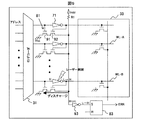
図1には、上記メモリ123の構成例が示される。
FIG. 1 shows a configuration example of the
図1に示されるように上記メモリ123は、行デコーダ31、列デコーダ32、列選択回路34、センスアンプ回路35、及びメモリマット33を含む。メモリマット33は、複数のワード線WLとそれに交差するように配置された複数のビット線とを含む。ビット線は、メモリマット33の1バイト(byte)毎に8本設けられる。行デコーダ31は、入力されたアドレス信号をデコードして、上記複数のワード線WLから1本のワード線を選択するための選択信号を形成する。列デコーダ32は、入力されたアドレス信号をデコードして列選択信号を形成する。列選択回路34は、上記列選択信号に基づいてビット線を選択する。選択されたビット線の信号は、センスアンプ回路35で増幅されてから、出力回路38を介してバス129に出力される(OUT)。また、異常検出回路36が設けられ、この異常検出回路36は、上記メモリマットからの情報読み出しが正常か否かを判定してエラー信号ERRを形成する。上記メモリマットからの情報読み出しが正常で無い場合、エラー信号ERRがアサートされる。さらに、コントローラ37が設けられ、このコントローラ37はこのメモリ123の全体的な動作制御を司る。
As shown in FIG. 1, the
上記メモリマット33には、通常のビット線とは別に、2本の異常検出用ラインRL0,RL1が設けられる。この2本の異常検出用ラインRL0,RL1は、図1において右側端部に配置される。異常検出用ラインRL0は、論理値“0”異常検出のために設けられ、論理値“0”が得られるようになっている。異常検出用ラインRL1は、論理値“1”の異常検出のために設けられ、論理値“1”が得られるようになっている。メモリ123のリード動作時には必ずこの異常検出用ラインRL0,RL1の信号が列選択回路34によって選択され、その論理値が異常検出回路36で判断されることで異常検出が可能とされる。異常検出用ラインRL0の論理値“0”、及び異常検出用ラインRL1の論理値“1”がそれぞれ正しく得られれば、メモリ123は正常動作していると判断される。しかし、異常検出用ラインRL0の論理値“0”、又は検出ラインRL1の論理値“1”が正しく得られない場合には、異常動作と判断され、エラー信号ERRがアサートされる。
The
ここで、図1に示されるように異常検出用ラインRL0,RL1をメモリマット33の端部に配置する構成では、メモリマット33全体に影響を及ぼすようなアタック(異常電圧、異常周波数印加や異常温度での動作)には有効である。しかし、レーザー照射等、メモリマット上の一部領域の誤動作を引き起こすような局所的なアタックに対しては、それを検出できないことが考えられる。そのため、局所的なアタックに対応するには、図2に示されるように、メモリマット33の端部の異常検出用ラインRL0,RL1とは別に、メモリマット33の数ビット毎、例えば1バイト(byte)毎に、異常検出用ラインRL0,RL1を配置するのが望ましい。このようにすれば、メモリマット33において多数の異常検出用ラインRL0,RL1が密に配置されるため、メモリマット33の局所的なアタックに対しても十分に対応することができる。
Here, as shown in FIG. 1, in the configuration in which the abnormality detection lines RL0 and RL1 are arranged at the end of the
尚、図2に示されるようにメモリマット33において異常検出用ラインRL0,RL1が密に配置されると、その分だけメモリマット33の面積や消費電流が増加してしまうため、求めるセキュリティのレベルやメモリの特性に応じて異常検出用ラインRL0,RL1の配置本数を決定するのが望ましい。メモリの特性とは、例えばアタックによるリードデータの変化が論理値“0”から論理値“1”もしくはそれとは逆の論理値“1”から論理値“0”のどちらか一方しか発生しないことを指し、このようなことが明かである場合には、配置する異常検出用ラインは論理値“0”又は論理値“1”の片方だけで十分となる。例えば、メモリマット33の端部の異常検出用ラインRL0,RL1はそのまま設け、メモリマット33の数ビット毎には、異常検出用ラインRL0,RL1の何れか一方のみを設ける構成が効果的と考えられる。例えば、電位保持状態が“1”であるメモリセルにレーザーを照射した場合、本来ならばビット線をディスチャージしないはずが誤動作によりディスチャージしてしまうとリードデータは“1”から“0”に変化してしまう。レーザー照射によるデータ化けがこの“0”化けメインである場合はRL1をRL0の配置本数に比較し、より多数設けることにより、レーザー照射によるアタック検出効率を向上させることが可能となる。逆に、電位保持状態が“0”であるメモリセルの“1”化け(ディスチャージするはずが、ディスチャージされない)がデータ化けのメインであるならば、RL0をより多数設けることが有効である。
As shown in FIG. 2, if the abnormality detection lines RL0 and RL1 are densely arranged in the
次に、上記異常検出用ラインRL0,RL1の形成について説明する。 Next, the formation of the abnormality detection lines RL0 and RL1 will be described.
メモリ123がマスクROMとされる場合、異常検出用ラインRL0,RL1はインプラ方式やビア方式によって形成することができる。
When the
例えばインプラ方式の場合、図3(A)に示されるように、異常検出用ラインRL0に結合されている全てのメモリセルMCに対してはイオン注入により、論理値“0”の書込みを行い、異常検出用ラインRL1に結合されている全てのメモリセルMCに対してはイオン非注入により、論理値“1”の書込みを行えば良い。また、ビア方式の場合、図3(B)に示されるように、異常検出用ラインRL0に結合されている全てのメモリセルMCに対しては低電位側電源VSSラインに結合させることにより、論理値“0”の書込みを行い、異常検出用ラインRL1に結合されている全てのメモリセルMCに対しては低電位側電源VSSラインへの配線を省略することにより、論理値“1”の書込みを行えば良い。何れの場合においても、データ保持の対象となる通常のビット線BLは、それぞれ異常検出用ラインとワード線が共通とされ、各メモリセルMCにおいては、“0”または“1”の任意のデータを保持可能に構成される。 For example, in the case of the implantation method, as shown in FIG. 3A, the logic value “0” is written to all the memory cells MC coupled to the abnormality detection line RL0 by ion implantation. All the memory cells MC coupled to the abnormality detection line RL1 may be written with a logical value “1” by non-ion implantation. Further, in the case of the via method, as shown in FIG. 3B, all the memory cells MC coupled to the abnormality detection line RL0 are coupled to the low potential side power supply VSS line, so that Writing the value “0” and writing the logical value “1” to all the memory cells MC coupled to the abnormality detection line RL1 by omitting wiring to the low potential side power supply VSS line. Just do it. In any case, the normal bit line BL that is the object of data retention has a common abnormality detection line and word line, and any data of “0” or “1” is stored in each memory cell MC. It is configured to be able to hold.
メモリ123がEEPROMとされる場合に、図4に示されるように、異常検出用ラインRL0は、それに結合される全てのメモリセルMCに対して論理値“0”の書込みを行えば良く、また、異常検出用ラインRL1は、それに結合される全てのメモリセルMCを消去済のまま(論理値“1”)とすれば良い。図示はしないが、図3と同様に、図4における通常のビット線は、それぞれ異常検出用ラインとワード線が共通とされ、各メモリセルMCにおいては、“0”または“1”の任意のデータを保持可能に構成される。
When the
図5には、図1及び図2における異常検出回路36及びその周辺のさらに詳細な構成が示される。
FIG. 5 shows a more detailed configuration of the
図5に示されるように、1本の異常検出用ラインRL0毎に、トランスファゲート301とインバータ302が設けられる。トランスファゲート301はpチャネル型MOSトランジスタとnチャネル型MOSトランジスタとが並列接続されて成る。トランスファゲート301は列デコーダ32からの列選択信号SELによってオンオフ制御される。トランスファゲート301を構成するpチャネル型MOSトランジスタとnチャネル型MOSトランジスタとを同時にオン又はオフさせるためにインバータ302によって列選択信号SELの論理反転が行われる。上記トランスファゲート301とインバータ302とは、図2における列選択回路34の一部とされる。そして、リード信号REDによって動作制御されるnチャネル型MOSトランジスタ24が設けられ、上記トランスファゲート301と上記nチャネル型MOSトランジスタ24との間の信号伝達ラインを、プリチャージ信号CHGに応じて高電位側電源Vddレベルにプリチャージするためのpチャネル型MOSトランジスタ23が設けられる。上記プリチャージ信号CHGや上記リード信号REDはコントローラ37によって生成される。nチャネル型MOSトランジスタ24を設け、このnチャネル型MOSトランジスタ24を上記リード信号REDによって動作制御するのは、異常検出はリード動作時のみ行えば良いからである。センスアンプSAは、上記nチャネル型MOSトランジスタ24を介して伝達された信号を増幅するもので、図2に示されるセンスアンプ回路35の一部とされる。上記センスアンプSAの出力信号は異常検出回路36に伝達される。異常検出回路36は、オア回路25,26、ナンド回路27、及びフリップフロップ回路(FF)28とを含む。上記オア回路25における一つの入力端子に上記センスアンプSAの出力信号が伝達される。上記オア回路25における他の入力端子には、他の異常検出用ラインRL0に対応するセンスアンプの出力信号が伝達される。つまり、オア回路25では、メモリマット33における全ての異常検出用ラインRL0に対応するセンスアンプの出力信号のオア論理が求められることで、入力信号の論理値が期待値通りであるか否かの判定が行われる。例えばメモリマット33において複数配置された全ての異常検出用ラインRL0に対応するセンスアンプの出力信号の全てがローレベルとされる場合には、それは期待値通りであり、オア回路25の出力信号はローレベルとされる。しかし、メモリマット33に対するアタックに起因して、メモリマット33における全ての異常検出用ラインRL0のうちの少なくとも1本から論理値“0”の読み出しができない場合には、それは期待値と異なるため、オア回路25の出力信号はハイレベルとされる。オア回路25の出力は、フリップフロップ回路28のセット端子Sに伝達されて、このフリップフロップ回路28に保持される。オア回路25の出力は通常ローレベルであるが、オア回路25の出力がハイレベルの場合、フリップフロップ回路28によって、エラー信号ERRがハイレベルにアサートされる。尚、フリップフロップ回路28はリセット端子Rを有し、このリセット端子Rに供給されるリセット信号をアサートすることによって、フリップフロップ回路28を初期化することができる。
As shown in FIG. 5, a
図5では省略されているが、異常検出用ラインRL1に対応する回路は、異常検出用ラインRL0に対応する回路と同様に構成することができる。ただし、全ての異常検出用ラインRL1に対応するセンスアンプSAの出力信号は、ナンド回路27に伝達され、そこでナンド論理が得られることで、入力信号の論理値が期待値通りであるか否かの判定が行われる。この場合、メモリマット33に対するアタックに起因して、メモリマット33における全ての異常検出用ラインRL1のうちの少なくとも1本から論理値“1”の読み出しができない場合には、ナンド回路27の出力信号はハイレベルとされ、それがオア回路26介してフリップフロップ回路28に保持され、エラー信号ERRがハイレベルにアサートされる。
Although omitted in FIG. 5, the circuit corresponding to the abnormality detection line RL1 can be configured similarly to the circuit corresponding to the abnormality detection line RL0. However, the output signals of the sense amplifiers SA corresponding to all the abnormality detection lines RL1 are transmitted to the
次に、異常検出用ラインRL0,RL1の検出感度を向上させるための技術について説明する。 Next, a technique for improving the detection sensitivity of the abnormality detection lines RL0 and RL1 will be described.
異常検出用ラインの構成を通常のメモリ領域と同じ構成とした場合、プロセスばらつきやアタックによる影響の偏りによって、異常検出用ラインの論理値は正常にもかかわらず、通常のデータ記憶領域にエラーが発生することも考えられる。そのため、作りこみによって異常検出用ラインの特性をあらかじめ悪い(エラーが起こりやすい)状態にすることが考えられる。例えば、図6に示されるように、メモリセルを構成するMOSトランジスタの駆動能力を調整することにより、異常検出用ラインRL0,RL1のプリチャージ能力をメモリマット33における任意のデータを保持するビット線BLのプリチャージ能力よりも低くすると良い。また、ビット線BLに対応するプリチャージ用MOSトランジスタ61や、異常検出用ラインRL0,RL1に対応するプリチャージ用MOSトランジスタ23の駆動能力を調整することにより、異常検出用ラインRL0,RL1に結合されたメモリセルMCのディスチャージ能力をメモリマット33におけるビット線BLに結合されたメモリセルMCのディスチャージ能力よりも低くすると良い。このようにすれば、プロセスばらつきやアタックによる影響の偏りにかかわらず、適切な異常検出を行うことができる。
If the configuration of the abnormality detection line is the same as the normal memory area, an error will occur in the normal data storage area even though the logical value of the abnormality detection line is normal due to process variations and biased influences of attack. It can also occur. For this reason, it is conceivable that the characteristics of the abnormality detection line are made bad (error is likely to occur) in advance. For example, as shown in FIG. 6, by adjusting the driving capability of the MOS transistors constituting the memory cell, the precharge capability of the abnormality detection lines RL0 and RL1 is changed to a bit line for holding arbitrary data in the
上記例によれば、以下の作用効果を得ることができる。 According to the above example, the following operational effects can be obtained.
(1)メモリマット33の右側端部には、通常のビット線とは別に、2本の異常検出用ラインRL0,RL1が設けられる。異常検出用ラインRL0は、論理値“0”異常検出のために設けられ、異常検出用ラインRL1は、論理値“1”の異常検出のために設けられる。メモリ123のリード動作時には必ずこの異常検出用ラインRL0,RL1の信号が列選択回路34によって選択され、その論理値が異常検出回路36で判断されることで異常検出が行われる。異常検出用ラインRL0の論理値“0”、及び異常検出用ラインRL1の論理値“1”がそれぞれ正しく得られれば、メモリ123は正常動作していると判断される。しかし、異常検出用ラインRL0の論理値“0”、又は検出ラインRL1の論理値“1”が正しく得られない場合には異常とされ、エラー信号ERRがアサートされる。これにより、アタックに起因するメモリエラーの検出率の向上を図ることができる。
(1) Two abnormality detection lines RL0 and RL1 are provided at the right end portion of the
(2)メモリマット33の端部の異常検出用ラインRL0,RL1とは別に、メモリマット33の数ビット毎、例えば1バイト(byte)毎に、異常検出用ラインRL0,RL1を配置する。このようにすれば、メモリマット33において多数の異常検出用ラインRL0,RL1が密に配置されるため、メモリマット33の局所的なアタックに対しても十分に対応することができるので、メモリエラーの検出率をさらに向上させることができる。
(2) Apart from the abnormality detection lines RL0 and RL1 at the end of the
(3)メモリマット33において異常検出用ラインRL0,RL1が密に配置されると、その分だけメモリマット33の面積や消費電流が増加してしまうため、求めるセキュリティのレベルやメモリの特性に応じて異常検出用ラインRL0,RL1の配置本数を決定するのが望ましい。メモリの特性とは、例えばアタックによるリードデータの変化が論理値“0”から論理値“1”もしくはそれとは逆の論理値“1”から論理値“0”のどちらか一方しか発生しないことを指し、このようなことが明かである場合には、配置する異常検出用ラインは論理値“0”又は論理値“1”の片方だけで十分となる。例えば、メモリマット33の端部の異常検出用ラインRL0,RL1はそのまま設け、メモリマット33の数ビット毎には、異常検出用ラインRL0,RL1の何れか一方のみを設ける構成が効果的と考えられる。
(3) If the abnormality detection lines RL0 and RL1 are densely arranged in the
(4)メモリセルを構成するMOSトランジスタの駆動能力を調整することにより、異常検出用ラインRL0,RL1のプリチャージ能力をメモリマット33におけるビット線BLのプリチャージ能力よりも低くする。また、ビット線BLに対応するプリチャージ用MOSトランジスタ61や、異常検出用ラインRL0,RL1に対応するプリチャージ用MOSトランジスタ23の駆動能力を調整することにより、異常検出用ラインRL0,RL1に結合されたメモリセルMCのディスチャージ能力をメモリマット33におけるビット線BLに結合されたメモリセルMCのディスチャージ能力よりも低くする。それにより、プロセスばらつきやアタックによる影響の偏りにかかわらず、適切な異常検出を行うことができるので、メモリエラーの検出率を向上させることができる。
(4) By adjusting the drive capability of the MOS transistors constituting the memory cell, the precharge capability of the abnormality detection lines RL0 and RL1 is made lower than the precharge capability of the bit line BL in the
<実施の形態2>
実施の形態1では、メモリマット部におけるアタック対策について説明したが、実施の形態2では行デコーダにおけるアタック対策について説明する。
<Embodiment 2>
In the first embodiment, countermeasures against attacks in the memory mat unit have been described. In the second embodiment, countermeasures against attacks in the row decoder will be described.
レーザー照射により行デコーダ31が誤動作し、メモリエラーを生ずることが本願発明者によって確認されている。誤動作の発生箇所は、図7に示されるように、ワード線WLを選択レベルに駆動するためのドライバ部と推定され、ドライバ部のエラーにより、非選択であるはずのワード線が選択状態になっていると考えられる。例えばアドレスのデコード結果によりワード線WL−Aが選択されている状態でも、ワード線WL−Aに対応するメモリセルは接続されていないため、ビット線BLのレベルはハイ(H)レベルのままで変化しない。しかし、レーザー照射等のアタックによりドライバが誤動作した場合には、非選択であるはずのワード線WL−Bが選択レベルに駆動される可能性がある。このとき、ワード線WL−Bに結合されているメモリセルによってビット線BLがディスチャージされるため、ビット線BLはハイレベルからローレベルに変化してしまい、読み出しデータの論理値が期待値と異なるものとなってしまう。
It has been confirmed by the present inventor that the
そこで、図8に示されるように、各ドライバ71毎に、入力側論理と出力側論理とのモニタを可能とするモニタ回路81を搭載する。このモニタ回路81は、対応するドライバ71の入力側論理と出力側論理とを比較するための排他的論理和回路によって構成される。ドライバ71の入力側論理と出力側論理とが異なる場合には正常であり、ドライバ71の入力側論理と出力側論理とが一致する場合には異常である。全てのモニタ回路81の出力信号は、オア回路82を介して後段のフリップフロップ回路83に伝達され、このフリップフロップ回路83によってエラー信号ERRが形成されるようになっている。ドライバ71の入力側論理と出力側論理とが一致する場合、当該ドライバ71に対応するモニタ回路81の出力信号がハイレベルになり、それがオア回路82を介してフリップフロップ回路83に伝達されると、このフリップフロップ回路83によりエラー信号ERRがアサートされる。
Therefore, as shown in FIG. 8, a
上記の構成によれば、上記モニタ回路81によって、対応するドライバ71の力側論理と出力側論理とが一致するか否かを判別することで、非選択ワード線がレーザーによって選択レベルになった場合のみならず、選択ワード線がレーザーによって逆に非選択になった場合も、エラー検出することができる。
According to the configuration described above, the
図9には、上記モニタ回路81の別の構成例が示される。
FIG. 9 shows another configuration example of the
図9に示されるモニタ回路81は、二つのnチャネル型MOSトランジスタ91,92が直列接続されて成る。nチャネル型MOSトランジスタ91のゲート電極は、対応するドライバ71の入力端子に結合され、nチャネル型MOSトランジスタ92のゲート電極は対応するドライバ71の出力端子に結合される。nチャネル型MOSトランジスタ91のソース電極は低電位側電源Vssに結合され、nチャネル型MOSトランジスタ92のドレイン電極は、プルアップ抵抗R1を介して高電位側電源Vddに結合されるとともに、インバータ93を介してフリップフロップ回路83に結合される。かかる構成において、ドライバ71の入力側論理と出力側論理とが一致する場合、当該ドライバ71に対応するモニタ回路81において、二つのnチャネル型MOSトランジスタ91,92の双方が導通されることにより、インバータ93の入力端子側は、蓄積電荷が引き抜かれてハイ(H)レベルからロー(L)レベルに遷移される。これにより、インバータ93の出力がローレベルからハイレベルに遷移され、フリップフロップ回路83によってエラー信号ERRがアサートされる。
The
尚、上記の回路構成では、非選択ワード線の誤選択状態しか検出することができないが、図8に示される構成に比べて、モニタ回路81の回路規模の削減が可能である。
In the circuit configuration described above, only the erroneous selection state of the unselected word line can be detected, but the circuit scale of the
以上、行デコーダの異常を検出する方式について説明したが、列デコーダの誤動作検出も同様の方式で対応可能であると考えられる。 As described above, the method of detecting the abnormality of the row decoder has been described, but it is considered that the malfunction detection of the column decoder can be handled by the same method.
<実施の形態3>
メモリ123においては、読み出し時間短縮などの性能向上のために、内部で専用の電源電圧が生成される場合がある。例えば、ビット線選択のためのトランスファゲート301を導通させるために、電源回路102において、高電位側電源Vddよりも高レベルの電圧Vdd_eが生成される。電圧Vdd_eは、列デコーダ32からの選択信号SELに基づいてドライバ101の動作用電源電圧とされる。ドライバ101から出力されるハイレベルの電圧レベルはVdd_eレベルとされ、それは高電位側電源Vddよりも高レベルとされるため、導通されたトランスファゲート301のオン抵抗を小さく抑えることができる。トランスファゲート301のオン抵抗を小さく抑えることにより、ビット線BLのチャージや、ディスチャージを高速化している。かかる構成において、電源回路102へのレーザー照射によりその出力電圧レベルが変動することが、本願発明者によって確認されている。また、その電圧変動によって、トランスファゲート301が導通されない場合があり、かかる場合には、ビット線BLがディスチャージされないため、データを正しく読み出すことができなくなる。
<Embodiment 3>
In the
そこで、電源回路102において、電圧変動を検出可能な検出器を設けることで、メモリエラー検出率の向上を図ることができる。図11には、その場合の電源回路102の構成例が示される。
Therefore, by providing a detector capable of detecting voltage fluctuation in the
図11に示される電源回路102は、基準電圧Vrefを生成する基準電圧生成部111と、電源電圧Vdd_eを生成する電源電圧生成部112と、上記基準電圧Vrefと電源電圧Vdd_eとの比較を行うコンパレータ113と、このコンパレータ113の出力信号に基づいてエラー信号ERRを形成するフリップフロップ回路114とを含む。基準電圧Vrefを生成し、電源電圧Vdd_eの変動が、基準電圧Vrefを超えた場合はコンパレータ113の出力がハイレベルとなり、それがフリップフロップ回路114に保持されることで、エラー信号ERRがアサートされる。このとき基準電圧Vrefは、実際の読み出しエラーが発生する電圧変動より早く検出可能なレベルに設定するべきである。また、基準電圧Vrefを生成する基準電圧生成部111は、局所的なアタック(レーザー照射等)において、電源電圧生成部112と同時に影響を受けることにより、電圧変動の検出が不能になることを防止するため、基準電圧Vrefが変動しないように、電源電圧生成部112との間隔を十分に確保すると良い。さらに、図11において50で示されるように、アタックに起因する電圧変動を、基準電圧Vrefと電源電圧Vdd_eとで互いに逆位相にすることで、コンパレータ113での比較をより高感度で行うことができる。
11 includes a reference
以上本発明者によってなされた発明を具体的に説明したが、本発明はそれに限定されるものではなく、その要旨を逸脱しない範囲で種々変更可能であることはいうまでもない。 Although the invention made by the present inventor has been specifically described above, the present invention is not limited thereto, and it goes without saying that various changes can be made without departing from the scope of the invention.
31 行デコーダ
32 列デコーダ
33 メモリマット
34 列選択回路
35 センスアンプ回路
36 異常検出回路
37 コントローラ
38 出力回路
71 ドライバ
81 モニタ回路
83 フリップフロップ回路
111 基準電圧生成部
112 電源電圧生成部
113 コンパレータ
114 フリップフロップ回路
121 リセット端子
122 ポート
123 メモリ
124 システムコントローラ
125 CPU
126〜128 モジュール
RL0,RL1 異常検出用ライン
WL ワード線
BL ビット線
31
126 to 128 modules RL0, RL1 Abnormality detection line WL Word line BL Bit line
Claims (7)
上記記憶部は、それぞれ情報の記憶を可能とする複数のメモリセルが配列されて成るメモリマットと、
上記メモリマットからの情報読み出しが正常か否かを判定してエラー信号を形成するための第1異常検出回路と、を含み、
上記メモリマットは、上記メモリマットからの情報読み出しの際に、上記第1異常検出回路での判定に用いられる情報を出力可能な第1異常検出用ラインと第2異常検出用ラインとを含み、
上記第1異常検出用ラインには、上記第1異常検出用ラインを論理値”0”にするための第1メモリセルが結合され、上記第2異常検出力用ラインには、上記第2異常検出用ラインを論理値”1”にするための第2メモリセルが結合されて成ることを特徴とする半導体集積回路装置。 A semiconductor integrated circuit device including a storage unit capable of storing information,
The storage unit includes a memory mat in which a plurality of memory cells each capable of storing information are arranged;
A first abnormality detection circuit for determining whether or not information reading from the memory mat is normal and forming an error signal,
The memory mat includes a first abnormality detection line and a second abnormality detection line capable of outputting information used for determination by the first abnormality detection circuit when reading information from the memory mat,
A first memory cell for setting the first abnormality detection line to a logical value “0” is coupled to the first abnormality detection line, and the second abnormality detection power line is connected to the second abnormality detection line. 2. A semiconductor integrated circuit device comprising: a second memory cell for connecting a detection line to a logical value “1”;
上記第2異常検出用ラインから得られた信号の論理値が期待値通りであるか否かを判定するための第2判定回路と、を含む請求項1記載の半導体集積回路装置。 The first abnormality detection circuit includes a first determination circuit for determining whether or not a logical value of a signal obtained from the first abnormality detection line is as expected.
The semiconductor integrated circuit device according to claim 1, further comprising: a second determination circuit configured to determine whether a logical value of a signal obtained from the second abnormality detection line is as expected.
上記行デコーダの出力信号に基づいて、上記メモリマットに含まれるワード線を駆動するための第1ドライバと、
上記第1ドライバの入力側の論理レベルと出力側の論理レベルとを比較してエラー信号を形成するための第2異常検出回路と、を含む請求項1記載の半導体集積回路装置。 The memory unit includes a row decoder for decoding an input address signal;
A first driver for driving a word line included in the memory mat based on an output signal of the row decoder;
The semiconductor integrated circuit device according to claim 1, further comprising: a second abnormality detection circuit configured to compare an input side logic level and an output side logic level of the first driver to form an error signal.
上記電源回路によって形成された動作用電源電圧を所定の基準電圧と比較してエラー信号を形成するための第3異常検出回路と、を含む請求項1記載の半導体集積回路装置。 The memory unit includes a power supply circuit for forming a power supply voltage for operation of a main part of the memory unit;
The semiconductor integrated circuit device according to claim 1, further comprising: a third abnormality detection circuit configured to compare an operation power supply voltage formed by the power supply circuit with a predetermined reference voltage to form an error signal.
上記エラー信号に基づいて、上記CPUの動作を制御可能なシステムコントローラと、を含む請求項1記載の半導体集積回路装置。 A CPU accessible to the memory unit;
The semiconductor integrated circuit device according to claim 1, further comprising: a system controller capable of controlling the operation of the CPU based on the error signal.
Priority Applications (1)
| Application Number | Priority Date | Filing Date | Title |
|---|---|---|---|
| JP2008089301A JP5179923B2 (en) | 2008-03-31 | 2008-03-31 | Semiconductor integrated circuit device |
Applications Claiming Priority (1)
| Application Number | Priority Date | Filing Date | Title |
|---|---|---|---|
| JP2008089301A JP5179923B2 (en) | 2008-03-31 | 2008-03-31 | Semiconductor integrated circuit device |
Publications (2)
| Publication Number | Publication Date |
|---|---|
| JP2009245496A true JP2009245496A (en) | 2009-10-22 |
| JP5179923B2 JP5179923B2 (en) | 2013-04-10 |
Family
ID=41307220
Family Applications (1)
| Application Number | Title | Priority Date | Filing Date |
|---|---|---|---|
| JP2008089301A Expired - Fee Related JP5179923B2 (en) | 2008-03-31 | 2008-03-31 | Semiconductor integrated circuit device |
Country Status (1)
| Country | Link |
|---|---|
| JP (1) | JP5179923B2 (en) |
Citations (4)
| Publication number | Priority date | Publication date | Assignee | Title |
|---|---|---|---|---|
| JPS6188551A (en) * | 1984-10-08 | 1986-05-06 | Nec Corp | Detecting circuit for abnormal voltage |
| JPS6478176A (en) * | 1987-09-21 | 1989-03-23 | Mitsubishi Electric Corp | Semiconductor integrated circuit |
| JP2801933B2 (en) * | 1989-10-20 | 1998-09-21 | 富士通株式会社 | Semiconductor storage device |
| WO2006120310A1 (en) * | 2005-05-09 | 2006-11-16 | Stmicroelectronics Sa | Device for protecting a memory against fault-injection attacks |
-
2008
- 2008-03-31 JP JP2008089301A patent/JP5179923B2/en not_active Expired - Fee Related
Patent Citations (5)
| Publication number | Priority date | Publication date | Assignee | Title |
|---|---|---|---|---|
| JPS6188551A (en) * | 1984-10-08 | 1986-05-06 | Nec Corp | Detecting circuit for abnormal voltage |
| JPS6478176A (en) * | 1987-09-21 | 1989-03-23 | Mitsubishi Electric Corp | Semiconductor integrated circuit |
| JP2801933B2 (en) * | 1989-10-20 | 1998-09-21 | 富士通株式会社 | Semiconductor storage device |
| WO2006120310A1 (en) * | 2005-05-09 | 2006-11-16 | Stmicroelectronics Sa | Device for protecting a memory against fault-injection attacks |
| JP2008541257A (en) * | 2005-05-09 | 2008-11-20 | ストミクロエレクトロニクス・ソシエテ・アノニム | A device that protects memory against attacks caused by error injection |
Also Published As
| Publication number | Publication date |
|---|---|
| JP5179923B2 (en) | 2013-04-10 |
Similar Documents
| Publication | Publication Date | Title |
|---|---|---|
| US10019312B2 (en) | Error monitoring of a memory device containing embedded error correction | |
| CN105589762B (en) | Memory device, memory module and method for error correction | |
| US9940457B2 (en) | Detecting a cryogenic attack on a memory device with embedded error correction | |
| US8843732B2 (en) | Mechanism for detecting a no-processor swap condition and modification of high speed bus calibration during boot | |
| KR101977733B1 (en) | Method of detecting fault attack | |
| JP2008513925A (en) | Method and apparatus for protecting integrated circuits from erroneous operation | |
| US9529667B2 (en) | DRAM error correction event notification | |
| US8908464B2 (en) | Protection for system configuration information | |
| KR20090036182A (en) | Memory device for detecting light attack and method thereof | |
| US11410713B2 (en) | Apparatuses and methods for detecting illegal commands and command sequences | |
| KR20100000647A (en) | Flash memory device using an ecc algorithm and operating method thereof | |
| KR20170090177A (en) | Memory system, semiconductor memory device and operating method thereof | |
| US11443820B2 (en) | Memory device, memory address decoder, system, and related method for memory attack detection | |
| US20140003167A1 (en) | Nonvolatile memory device, operating method thereof, and data storage device having the same | |
| US9824732B2 (en) | Memory system with encoding | |
| JP2005056394A (en) | Storage device and memory card | |
| US20060206764A1 (en) | Memory reliability detection system and method | |
| CN111630601B (en) | Security enhancement for memory controllers | |
| JP5179923B2 (en) | Semiconductor integrated circuit device | |
| US11907062B2 (en) | Error check scrub operation method and semiconductor system using the same | |
| JP2008541257A (en) | A device that protects memory against attacks caused by error injection | |
| US20210279122A1 (en) | Lifetime telemetry on memory error statistics to improve memory failure analysis and prevention | |
| JP4100985B2 (en) | Data processing device, semiconductor memory device, and clock frequency detection method | |
| JP2009176393A (en) | Nonvolatile semiconductor storage device and its automatic test method | |
| KR19980078113A (en) | Package Self Burn-In Device |
Legal Events
| Date | Code | Title | Description |
|---|---|---|---|
| A711 | Notification of change in applicant |
Free format text: JAPANESE INTERMEDIATE CODE: A712 Effective date: 20100527 |
|
| A621 | Written request for application examination |
Free format text: JAPANESE INTERMEDIATE CODE: A621 Effective date: 20110301 |
|
| A977 | Report on retrieval |
Free format text: JAPANESE INTERMEDIATE CODE: A971007 Effective date: 20120928 |
|
| A131 | Notification of reasons for refusal |
Free format text: JAPANESE INTERMEDIATE CODE: A131 Effective date: 20121011 |
|
| A521 | Written amendment |
Free format text: JAPANESE INTERMEDIATE CODE: A523 Effective date: 20121210 |
|
| A01 | Written decision to grant a patent or to grant a registration (utility model) |
Free format text: JAPANESE INTERMEDIATE CODE: A01 Effective date: 20121227 |
|
| A61 | First payment of annual fees (during grant procedure) |
Free format text: JAPANESE INTERMEDIATE CODE: A61 Effective date: 20130110 |
|
| S531 | Written request for registration of change of domicile |
Free format text: JAPANESE INTERMEDIATE CODE: R313531 |
|
| R350 | Written notification of registration of transfer |
Free format text: JAPANESE INTERMEDIATE CODE: R350 |
|
| LAPS | Cancellation because of no payment of annual fees |