JP2009236865A - Thermal-type infrared solid-state imaging element and manufacturing method of the same - Google Patents
Thermal-type infrared solid-state imaging element and manufacturing method of the same Download PDFInfo
- Publication number
- JP2009236865A JP2009236865A JP2008086526A JP2008086526A JP2009236865A JP 2009236865 A JP2009236865 A JP 2009236865A JP 2008086526 A JP2008086526 A JP 2008086526A JP 2008086526 A JP2008086526 A JP 2008086526A JP 2009236865 A JP2009236865 A JP 2009236865A
- Authority
- JP
- Japan
- Prior art keywords
- diaphragm
- sacrificial layer
- infrared
- state imaging
- substrate
- Prior art date
- Legal status (The legal status is an assumption and is not a legal conclusion. Google has not performed a legal analysis and makes no representation as to the accuracy of the status listed.)
- Granted
Links
- 238000003384 imaging method Methods 0.000 title claims abstract description 52
- 238000004519 manufacturing process Methods 0.000 title claims abstract description 32
- 239000000758 substrate Substances 0.000 claims abstract description 53
- 238000001514 detection method Methods 0.000 claims abstract description 26
- 238000010521 absorption reaction Methods 0.000 claims abstract description 12
- 230000001681 protective effect Effects 0.000 claims description 45
- 238000000059 patterning Methods 0.000 claims description 24
- 239000000463 material Substances 0.000 claims description 18
- 238000000034 method Methods 0.000 claims description 17
- 230000037303 wrinkles Effects 0.000 claims description 17
- 239000004642 Polyimide Substances 0.000 claims description 13
- 229920001721 polyimide Polymers 0.000 claims description 13
- 239000004020 conductor Substances 0.000 claims description 8
- 230000037373 wrinkle formation Effects 0.000 claims description 8
- 230000000630 rising effect Effects 0.000 claims description 6
- 239000000126 substance Substances 0.000 claims description 3
- 239000007787 solid Substances 0.000 claims 1
- 239000010408 film Substances 0.000 description 119
- 239000010409 thin film Substances 0.000 description 17
- 229910052751 metal Inorganic materials 0.000 description 16
- 239000002184 metal Substances 0.000 description 16
- 150000004767 nitrides Chemical class 0.000 description 13
- 238000005530 etching Methods 0.000 description 11
- 229910052782 aluminium Inorganic materials 0.000 description 8
- XAGFODPZIPBFFR-UHFFFAOYSA-N aluminium Chemical compound [Al] XAGFODPZIPBFFR-UHFFFAOYSA-N 0.000 description 8
- 239000004071 soot Substances 0.000 description 8
- 230000015572 biosynthetic process Effects 0.000 description 7
- 230000000694 effects Effects 0.000 description 7
- NBIIXXVUZAFLBC-UHFFFAOYSA-N Phosphoric acid Chemical compound OP(O)(O)=O NBIIXXVUZAFLBC-UHFFFAOYSA-N 0.000 description 6
- 229920002120 photoresistant polymer Polymers 0.000 description 6
- 229910004298 SiO 2 Inorganic materials 0.000 description 5
- 238000005268 plasma chemical vapour deposition Methods 0.000 description 5
- 229910021420 polycrystalline silicon Inorganic materials 0.000 description 5
- 229920005591 polysilicon Polymers 0.000 description 5
- LIVNPJMFVYWSIS-UHFFFAOYSA-N silicon monoxide Chemical compound [Si-]#[O+] LIVNPJMFVYWSIS-UHFFFAOYSA-N 0.000 description 5
- 230000018109 developmental process Effects 0.000 description 4
- 238000001312 dry etching Methods 0.000 description 4
- 238000010438 heat treatment Methods 0.000 description 4
- 230000035945 sensitivity Effects 0.000 description 4
- WGTYBPLFGIVFAS-UHFFFAOYSA-M tetramethylammonium hydroxide Chemical compound [OH-].C[N+](C)(C)C WGTYBPLFGIVFAS-UHFFFAOYSA-M 0.000 description 4
- 238000001039 wet etching Methods 0.000 description 4
- RTAQQCXQSZGOHL-UHFFFAOYSA-N Titanium Chemical compound [Ti] RTAQQCXQSZGOHL-UHFFFAOYSA-N 0.000 description 3
- 229910000147 aluminium phosphate Inorganic materials 0.000 description 3
- 238000010586 diagram Methods 0.000 description 3
- 239000012528 membrane Substances 0.000 description 3
- 230000007261 regionalization Effects 0.000 description 3
- 229910052719 titanium Inorganic materials 0.000 description 3
- 239000010936 titanium Substances 0.000 description 3
- 235000012431 wafers Nutrition 0.000 description 3
- KRHYYFGTRYWZRS-UHFFFAOYSA-N Fluorane Chemical compound F KRHYYFGTRYWZRS-UHFFFAOYSA-N 0.000 description 2
- OAKJQQAXSVQMHS-UHFFFAOYSA-N Hydrazine Chemical compound NN OAKJQQAXSVQMHS-UHFFFAOYSA-N 0.000 description 2
- VEXZGXHMUGYJMC-UHFFFAOYSA-N Hydrochloric acid Chemical compound Cl VEXZGXHMUGYJMC-UHFFFAOYSA-N 0.000 description 2
- XHCLAFWTIXFWPH-UHFFFAOYSA-N [O-2].[O-2].[O-2].[O-2].[O-2].[V+5].[V+5] Chemical compound [O-2].[O-2].[O-2].[O-2].[O-2].[V+5].[V+5] XHCLAFWTIXFWPH-UHFFFAOYSA-N 0.000 description 2
- 230000005540 biological transmission Effects 0.000 description 2
- 230000006866 deterioration Effects 0.000 description 2
- 210000002414 leg Anatomy 0.000 description 2
- 230000005855 radiation Effects 0.000 description 2
- 238000004544 sputter deposition Methods 0.000 description 2
- OGIDPMRJRNCKJF-UHFFFAOYSA-N titanium oxide Inorganic materials [Ti]=O OGIDPMRJRNCKJF-UHFFFAOYSA-N 0.000 description 2
- 229910052720 vanadium Inorganic materials 0.000 description 2
- LEONUFNNVUYDNQ-UHFFFAOYSA-N vanadium atom Chemical compound [V] LEONUFNNVUYDNQ-UHFFFAOYSA-N 0.000 description 2
- 229910001935 vanadium oxide Inorganic materials 0.000 description 2
- RYGMFSIKBFXOCR-UHFFFAOYSA-N Copper Chemical compound [Cu] RYGMFSIKBFXOCR-UHFFFAOYSA-N 0.000 description 1
- ZOKXTWBITQBERF-UHFFFAOYSA-N Molybdenum Chemical compound [Mo] ZOKXTWBITQBERF-UHFFFAOYSA-N 0.000 description 1
- 229910052581 Si3N4 Inorganic materials 0.000 description 1
- VYPSYNLAJGMNEJ-UHFFFAOYSA-N Silicium dioxide Chemical compound O=[Si]=O VYPSYNLAJGMNEJ-UHFFFAOYSA-N 0.000 description 1
- XUIMIQQOPSSXEZ-UHFFFAOYSA-N Silicon Chemical compound [Si] XUIMIQQOPSSXEZ-UHFFFAOYSA-N 0.000 description 1
- GWEVSGVZZGPLCZ-UHFFFAOYSA-N Titan oxide Chemical compound O=[Ti]=O GWEVSGVZZGPLCZ-UHFFFAOYSA-N 0.000 description 1
- 239000006096 absorbing agent Substances 0.000 description 1
- 238000004380 ashing Methods 0.000 description 1
- 210000001217 buttock Anatomy 0.000 description 1
- 229910052802 copper Inorganic materials 0.000 description 1
- 239000010949 copper Substances 0.000 description 1
- 230000003247 decreasing effect Effects 0.000 description 1
- 230000001419 dependent effect Effects 0.000 description 1
- PCHJSUWPFVWCPO-UHFFFAOYSA-N gold Chemical compound [Au] PCHJSUWPFVWCPO-UHFFFAOYSA-N 0.000 description 1
- 239000010931 gold Substances 0.000 description 1
- 229910052737 gold Inorganic materials 0.000 description 1
- 238000009413 insulation Methods 0.000 description 1
- 229910052750 molybdenum Inorganic materials 0.000 description 1
- 239000011733 molybdenum Substances 0.000 description 1
- 230000004297 night vision Effects 0.000 description 1
- 238000000206 photolithography Methods 0.000 description 1
- 238000000926 separation method Methods 0.000 description 1
- 229910052710 silicon Inorganic materials 0.000 description 1
- 239000010703 silicon Substances 0.000 description 1
- HQVNEWCFYHHQES-UHFFFAOYSA-N silicon nitride Chemical compound N12[Si]34N5[Si]62N3[Si]51N64 HQVNEWCFYHHQES-UHFFFAOYSA-N 0.000 description 1
- 229910052814 silicon oxide Inorganic materials 0.000 description 1
- 230000002195 synergetic effect Effects 0.000 description 1
- 238000001931 thermography Methods 0.000 description 1
- WFKWXMTUELFFGS-UHFFFAOYSA-N tungsten Chemical compound [W] WFKWXMTUELFFGS-UHFFFAOYSA-N 0.000 description 1
- 229910052721 tungsten Inorganic materials 0.000 description 1
- 239000010937 tungsten Substances 0.000 description 1
Images


Classifications
-
- G—PHYSICS
- G01—MEASURING; TESTING
- G01J—MEASUREMENT OF INTENSITY, VELOCITY, SPECTRAL CONTENT, POLARISATION, PHASE OR PULSE CHARACTERISTICS OF INFRARED, VISIBLE OR ULTRAVIOLET LIGHT; COLORIMETRY; RADIATION PYROMETRY
- G01J5/00—Radiation pyrometry, e.g. infrared or optical thermometry
- G01J5/10—Radiation pyrometry, e.g. infrared or optical thermometry using electric radiation detectors
- G01J5/20—Radiation pyrometry, e.g. infrared or optical thermometry using electric radiation detectors using resistors, thermistors or semiconductors sensitive to radiation, e.g. photoconductive devices
-
- G—PHYSICS
- G01—MEASURING; TESTING
- G01J—MEASUREMENT OF INTENSITY, VELOCITY, SPECTRAL CONTENT, POLARISATION, PHASE OR PULSE CHARACTERISTICS OF INFRARED, VISIBLE OR ULTRAVIOLET LIGHT; COLORIMETRY; RADIATION PYROMETRY
- G01J5/00—Radiation pyrometry, e.g. infrared or optical thermometry
- G01J5/02—Constructional details
- G01J5/0225—Shape of the cavity itself or of elements contained in or suspended over the cavity
- G01J5/023—Particular leg structure or construction or shape; Nanotubes
-
- G—PHYSICS
- G01—MEASURING; TESTING
- G01J—MEASUREMENT OF INTENSITY, VELOCITY, SPECTRAL CONTENT, POLARISATION, PHASE OR PULSE CHARACTERISTICS OF INFRARED, VISIBLE OR ULTRAVIOLET LIGHT; COLORIMETRY; RADIATION PYROMETRY
- G01J5/00—Radiation pyrometry, e.g. infrared or optical thermometry
- G01J5/02—Constructional details
- G01J5/0225—Shape of the cavity itself or of elements contained in or suspended over the cavity
- G01J5/024—Special manufacturing steps or sacrificial layers or layer structures
-
- G—PHYSICS
- G01—MEASURING; TESTING
- G01J—MEASUREMENT OF INTENSITY, VELOCITY, SPECTRAL CONTENT, POLARISATION, PHASE OR PULSE CHARACTERISTICS OF INFRARED, VISIBLE OR ULTRAVIOLET LIGHT; COLORIMETRY; RADIATION PYROMETRY
- G01J5/00—Radiation pyrometry, e.g. infrared or optical thermometry
- G01J5/02—Constructional details
- G01J5/08—Optical arrangements
- G01J5/0853—Optical arrangements having infrared absorbers other than the usual absorber layers deposited on infrared detectors like bolometers, wherein the heat propagation between the absorber and the detecting element occurs within a solid
Abstract
Description
本発明は、熱分離構造を有する熱型赤外線固体撮像素子及びその製造方法に関し、特に、画素が開口率を向上するための庇構造を有する熱型赤外線固体撮像素子及びその製造方法に関する。 The present invention relates to a thermal infrared solid-state imaging device having a thermal separation structure and a method for manufacturing the same, and more particularly to a thermal infrared solid-state imaging device having a ridge structure for pixels to improve the aperture ratio and a method for manufacturing the same.
熱型赤外線固体撮像素子に用いられる熱型赤外線検出器を高感度化するため、小田による特開2001−215151号公報に記載された開口率を向上できる構造及び製造方法が提案されている。図4は従来の熱型赤外線固体撮像素子である上記特開2001−215151号公報に記載された熱型赤外線固体撮像素子の単位画素を示す電流経路に沿った断面構造図である。 In order to increase the sensitivity of a thermal infrared detector used in a thermal infrared solid-state imaging device, a structure and a manufacturing method that can improve the aperture ratio described in JP-A-2001-215151 by Oda have been proposed. FIG. 4 is a cross-sectional structure diagram along a current path showing a unit pixel of a thermal infrared solid-state imaging device described in Japanese Patent Laid-Open No. 2001-215151, which is a conventional thermal infrared solid-state imaging device.
信号読出回路27が形成されたSi集積回路基板1上に金属反射膜2が形成されており、該金属反射膜2を覆って第1の絶縁保護膜21が形成されている。Si集積回路基板1の第1絶縁保護膜21側の面の上方に赤外線受光部22(ダイアフラム)が複数配列される。各々の赤外線受光部22(ダイアフラム)は、2つの支持部6によって空洞部23を隔てて第1絶縁保護膜21の表面から浮かせられて支持されており、1つの画素に1つの赤外線受光部22(ダイアフラム)が配置されている。赤外線受光部22(ダイアフラム)は、ボロメータ薄膜13(温度検出部)と、金属配線15のボロメータ薄膜13(温度検出部)に接した2つの電極部と、ボロメータ薄膜13(温度検出部)及び2つの電極部を取り囲む絶縁保護膜24,25,26とから構成されている。支持部6は、Si集積回路基板1表面に対して平行な梁6aと、梁6aの一端に接続された支持脚6bとから成り、金属配線15を絶縁保護膜24,25,26で取り囲んだ構造になっている。梁6aは、図4では非常に短いように描かれているが、実際には、熱コンダクタンスを小さくするために、赤外線受光部22(ダイアフラム)の少なくとも1辺に渡って引き延ばされ、一端が赤外線受光部22(ダイアフラム)と繋がっている。金属配線15は、その一端は前述のように電極部としてボロメータ薄膜13(温度検出部)と電気的に接続されており、他端は信号読出回路27の接続電極3と電気的に接続されている。赤外線受光部22(ダイアフラム)の、Si集積回路基板1と反対側の面から庇部12が突出している。庇部12は、赤外線受光部22(ダイアフラム)内の電極部との間、支持部6との間、及びSi集積回路基板1の接続電極3との間に空間を隔てて、電極部、支持部6、及び接続電極3を覆うように延びている。
A metal reflective film 2 is formed on the Si
赤外線受光部22(ダイアフラム)の絶縁保護膜24,25,26と庇部12に赤外線が入射すると、赤外線の一部が絶縁保護膜24,25,26と庇部12のそれぞれで吸収されて、絶縁保護膜24,25,26及び庇部12が加熱される。絶縁保護膜24,25,26と庇部12に入射した赤外線の他の部分は、赤外線受光部22(ダイアフラム),庇部12,支持部6をそれぞれ透過してSi集積回路基板1側に向かって進行する。赤外線受光部22(ダイアフラム),庇部12,支持部6をそれぞれ透過した赤外線は、金属反射膜2や金属配線15及び接続電極3により赤外線受光部22(ダイアフラム)及び庇部12に向けて反射されて、再び絶縁保護膜24,25,26と庇部12に入射する。これにより、金属反射膜2によって反射された赤外線が絶縁保護膜24,25,26と庇部12に吸収されて、絶縁保護膜24,25,26及び庇部12がさらに加熱される。庇部12の熱は、絶縁保護膜25,26を通してボロメータ薄膜13(温度検出部)に伝わる。このように庇部12及び絶縁保護膜24,25,26からの熱によりボロメータ薄膜13(温度検出部)の温度が変化して、ボロメータ薄膜13(温度検出部)の抵抗値が変化する。この抵抗値の変化は、Si集積回路基板1内の信号読出回路27により電圧変化に変換されて電気信号として読み出され、その電気信号を基に外部回路により赤外画像化される。
When infrared rays are incident on the insulating
本画素構造では、赤外線受光部22(ダイアフラム)から庇部12が突出し、その庇部12で、電極部及び支持部6の、Si集積回路基板1側と反対側のそれぞれの面や、接続電極3を、空間を隔てて覆っているので、各画素の開口率が増加し、赤外線をより多く吸収でき、高感度にできている。
In this pixel structure, the
上述した従来技術においては、赤外線受光部(ダイアフラム)の絶縁保護膜,支持部の絶縁保護膜及び庇部は何れもシリコン窒化膜,シリコン酸化膜またはシリコン酸窒化膜より形成される。これらのうち、赤外線受光部(ダイアフラム)を構成する絶縁保護膜と支持部を構成する絶縁保護膜とは同層の前記絶縁膜で形成されるが、庇部は赤外線受光部内の電極部との間、支持部との間、及びSi集積回路基板の接続電極との間に空間を隔てて、電極部、支持部、及び接続電極を覆うように延びている構造を持つため、赤外線受光部(ダイアフラム)や支持部とは別層の前記絶縁膜で形成される。そのため、製造過程において赤外線受光部(ダイアフラム)上に直接堆積され、開口率向上に寄与しない庇形成用絶縁膜不要部分が存在し、これをそのまま残すと赤外線受光部(ダイアフラム)の無意味な熱容量増加があり、熱応答特性が低下するという問題がある。 In the prior art described above, the insulating protective film of the infrared light receiving portion (diaphragm), the insulating protective film of the support portion, and the collar portion are all formed of a silicon nitride film, a silicon oxide film, or a silicon oxynitride film. Among these, the insulating protective film that constitutes the infrared light receiving part (diaphragm) and the insulating protective film that constitutes the support part are formed of the same insulating layer, but the collar part is formed with the electrode part in the infrared light receiving part. Since it has a structure extending so as to cover the electrode part, the support part, and the connection electrode with a space between the support part and the connection electrode of the Si integrated circuit substrate, the infrared light receiving part ( The insulating film is formed in a layer separate from the diaphragm) and the support portion. Therefore, there is a part that does not contribute to improving the aperture ratio and is deposited directly on the infrared light receiving part (diaphragm) in the manufacturing process, and if left as it is, the infrared heat receiving part (diaphragm) has a meaningless heat capacity There is a problem that there is an increase and the thermal response characteristic is lowered.
この熱応答特性低下を避けるためには、赤外線受光部(ダイアフラム)上の中央付近に堆積された庇形成用絶縁膜不要部分を部分的にエッチング除去すれば良く、図4に示した従来の熱型赤外線固体撮像素子単位画素断面構造図においても、赤外線受光部(ダイアフラム)上に堆積された庇形成用絶縁膜不要部分が除去されている様子が描かれている。特開2001−215151号公報の記述によれば、庇形成用絶縁膜を庇部形状に加工する工程において、同時にこの赤外線受光部(ダイアフラム)上に直接堆積された庇形成用絶縁膜不要部分を部分的にエッチング除去している。この工程では、庇形成用絶縁膜を各画素毎の庇部に確実に切り分けなければならないため、庇形成用絶縁膜の膜厚以上にエッチングを進めるオーバーエッチングを充分に加える必要がある。そのため、特開2001−215151号公報の製造方法では赤外線受光部(ダイアフラム)を構成する絶縁保護膜の削られる量が多く、かつ、その制御が難しいため、画素間,ウエハ間,さらにはロット間での特性バラツキが大きくなるという問題がある。オーバーエッチングが多過ぎれば、赤外線受光部(ダイアフラム)の絶縁保護膜を突き破り、ボロメータ薄膜(温度検出部)を傷めてしまう危険性さえある。 In order to avoid this deterioration of the thermal response characteristics, it is only necessary to partially etch away the unnecessary portion of the soot-forming insulating film deposited near the center on the infrared light receiving portion (diaphragm). Also in the cross-sectional structure diagram of the unit infrared solid-state imaging device unit pixel, a state in which an unnecessary portion of the soot forming insulating film deposited on the infrared light receiving portion (diaphragm) is removed is illustrated. According to the description of Japanese Patent Application Laid-Open No. 2001-215151, in the step of processing the soot forming insulating film into the soot shape, the soot forming insulating film unnecessary portion directly deposited on the infrared light receiving part (diaphragm) is simultaneously removed. Etching is partially removed. In this process, since the soot forming insulating film must be surely cut into the soot for each pixel, it is necessary to sufficiently apply over-etching that advances etching beyond the thickness of the soot forming insulating film. For this reason, in the manufacturing method disclosed in Japanese Patent Laid-Open No. 2001-215151, the amount of the insulating protective film that forms the infrared light receiving section (diaphragm) is large and difficult to control, so that it is difficult to control between pixels, wafers, and lots. There is a problem that the characteristic variation in the case becomes large. If there is too much over-etching, there is a risk that the insulation protective film of the infrared light receiving part (diaphragm) will be broken through and the bolometer thin film (temperature detection part) will be damaged.
このような問題を回避するため、本願発明者等は特開2005−116856号公報及びUS 7,276,698 B2において、加工精度良く、画素間,ウエハ間,さらにはロット間での特性バラツキを抑えて、赤外線受光部(ダイアフラム)上に堆積される庇形成用絶縁膜不要部分を部分的に除去し、熱応答特性低下を抑え得る熱型赤外線固体撮像素子及びその製造方法を提案した。図5及び図6はUS 7,276,698 B2記載の熱型赤外線固体撮像素子の単位画素を示す模式的縦断面構造図及び単位画素平面図である。 In order to avoid such a problem, the inventors of the present application disclosed in Japanese Patent Application Laid-Open No. 2005-116856 and US Pat. No. 7,276,698 B2 with high processing accuracy and suppressed characteristic variations between pixels, wafers, and lots, and infrared rays. A thermal infrared solid-state imaging device and a method for manufacturing the same have been proposed that can partially remove the unnecessary portion of the soot-forming insulating film deposited on the light-receiving portion (diaphragm) and suppress deterioration in thermal response characteristics. 5 and 6 are a schematic longitudinal sectional view and a unit pixel plan view showing a unit pixel of a thermal infrared solid-state imaging device described in US Pat. No. 7,276,698 B2.
図5及び図6に示すように、庇部12はリング状の庇接続部18によってダイアフラム5と接着しており、その僅か内側にて庇開口部19が開けられている。図5の断面のように、庇部12は庇接続部18から庇開口部19に掛けてダイアフラム5から浮き上がっている。庇開口部19に元は存在した庇形成用絶縁膜不要部分が、ダイアフラム5中央部に島状に設けた犠牲層をエッチングストッパとして取り除かれるため、このような断面形状となっている。この犠牲層は、庇部12と支持部6等との間の空間を確保するための犠牲層と同時に形成される、すなわち同じ物である。エッチングストッパとなった犠牲層の残骸は、その後の犠牲層エッチング工程において他の犠牲層と同時に除去される。
As shown in FIGS. 5 and 6, the
従って、製造工程を複雑化させること無く、エッチングストッパを用いた庇形成用絶縁膜不要部分除去ができるので、赤外線受光部(ダイアフラム)を構成する絶縁保護膜が削られることは無く、画素間,ウエハ間,さらにはロット間での特性バラツキが大きくなるという問題が解決されている。 Therefore, since the unnecessary part of the insulating film for forming the ridges using the etching stopper can be removed without complicating the manufacturing process, the insulating protective film constituting the infrared light receiving part (diaphragm) is not scraped, and between pixels, The problem that the characteristic variation between wafers and also between lots becomes large is solved.
前述した特開2001−215151号公報,特開2005−116856号公報及びUS 7,276,698 B2の熱型赤外線固体撮像素子においては、何れも庇部が一体物として構成されている。そのため、画素の熱応答特性の改善を図って庇部の膜厚を薄くすると、当該庇部の入射赤外線吸収力が減少してしまうと云う問題があった。 In the above-described thermal infrared solid-state imaging devices disclosed in JP-A-2001-215151, JP-A-2005-116856, and US Pat. No. 7,276,698 B2, the collar portion is configured as an integral body. For this reason, when the thermal response characteristic of the pixel is improved to reduce the thickness of the collar portion, there is a problem that the incident infrared ray absorbing power of the collar portion is reduced.
また、特開2005−116856号公報及びUS 7,276,698 B2の熱型赤外線固体撮像素子における画素の庇接続部は、フォトリソグラフィー技術による犠牲層の接続領域開口により形状寸法が決定される。犠牲層としては、感光性ポリイミド・ポリシリコン・アルミニウムと云ったものが用いられる。感光性ポリイミドの場合は直接露光によるパターン形成であり、ポリシリコンやアルミニウムでは、まずそれらの上に塗布したフォトレジストへ露光・パターン形成し、続いてエッチングによるポリシリコンやアルミニウムへのパターン形成となる。感光性ポリイミドやフォトレジストへ露光装置で装置限界付近の極狭い隙間をパターン形成する場合、回折効果によって隙間が拡がってしまい、露光マスク寸法通りに形成することが極めて難しい。その拡がりを考慮しなければならないため、ダイアフラムエッジから庇接続部までのマージン及び庇接続部から庇開口部までのマージンを大きく設定しなければならないと云う問題があった。ダイアフラムエッジから庇接続部までの領域,庇接続部,及び庇接続部から庇開口部までの領域はダイアフラムとオーバーラップしている所なので、これらの領域には庇部が無くても赤外線吸収に支障は無い。従って、これらの領域が大きい分は無駄に熱応答特性を低下させていることになる。 In addition, the shape of the pixel connecting portion of the thermal infrared solid-state imaging device disclosed in Japanese Patent Laid-Open No. 2005-116856 and US Pat. No. 7,276,698 B2 is determined by the opening of the connection region of the sacrificial layer by photolithography. As the sacrificial layer, a material such as photosensitive polyimide, polysilicon, and aluminum is used. In the case of photosensitive polyimide, pattern formation is performed by direct exposure, and in the case of polysilicon or aluminum, first, exposure and pattern formation are performed on the photoresist applied on them, followed by pattern formation on polysilicon or aluminum by etching. . When a very narrow gap near the device limit is formed by patterning on a photosensitive polyimide or photoresist with an exposure apparatus, the gap is widened due to the diffraction effect, and it is extremely difficult to form according to the exposure mask dimensions. Since the spread has to be taken into account, there is a problem that a margin from the diaphragm edge to the heel connection portion and a margin from the heel connection portion to the heel opening portion must be set large. Since the area from the diaphragm edge to the heel connection, the heel connection, and the area from the heel connection to the heel opening overlap with the diaphragm, these areas can absorb infrared light even if there is no heel. There is no hindrance. Therefore, the larger the area, the lower the heat response characteristic is wasted.
本発明は、上記問題点に鑑みてなされたものであって、その主たる目的は、上述したような庇構造を持つ熱型赤外線検出器を単位画素とする熱型赤外線固体撮像素子及びその製造方法に関し、該庇部の入射赤外線吸収力を減少させること無く、むしろそれの向上を図ることができ、尚且つ、画素の熱応答特性を改善できる熱型赤外線固体撮像素子及びその製造方法を提供することにある。 The present invention has been made in view of the above problems, and its main object is a thermal infrared solid-state imaging device having a thermal infrared detector having a ridge structure as described above as a unit pixel, and a method for manufacturing the same. The present invention provides a thermal infrared solid-state imaging device and a method for manufacturing the same that can improve the thermal absorption characteristics of pixels without decreasing the incident infrared absorption power of the heel portion. There is.
前述の課題を解決するために本発明の熱型赤外線固体撮像素子は、基板に形成された信号読出のための集積回路に接続される配線を含む支持部により、前記配線に接続される温度検出部を含むダイアフラムが、前記基板から浮いた状態で支持される赤外線検出素子が複数配置された熱型赤外線固体撮像素子において、前記ダイアフラムの外周近傍に接続され、該外周近傍から空中に立ち上がり、前記ダイアフラムの外側に延びる庇部を備え、前記庇部は、前記ダイアフラムの外側に延びる第1の部位が、前記ダイアフラムの外周近傍に接続される第2の部位及び該外周近傍から空中に立ち上がる第3の部位よりも、厚く形成されていることを特徴とする。 In order to solve the above-described problems, a thermal infrared solid-state imaging device according to the present invention has a temperature detection connected to the wiring by a support portion including a wiring connected to an integrated circuit for signal readout formed on a substrate. In a thermal infrared solid-state imaging device in which a plurality of infrared detection elements supported in a state where the diaphragm including the portion is floated from the substrate is connected to the vicinity of the outer periphery of the diaphragm, rising from the vicinity of the outer periphery to the air, A flange portion extending outside the diaphragm, wherein the flange portion has a first portion extending outside the diaphragm, a second portion connected to the vicinity of the outer periphery of the diaphragm, and a third portion rising in the air from the vicinity of the outer periphery. It is characterized by being formed thicker than the part.
また、本発明の熱型赤外線固体撮像素子は、信号読出のための集積回路が形成され、該集積回路との接続電極を備えた基板と、赤外線を吸収することにより加熱される赤外線吸収部、該赤外線吸収部からの熱によって温度が変化して前記赤外線吸収部の温度変化を検出する温度検出部、及び、該温度検出部と電気的に接続された電極部を備え、前記基板の一側の面上に間隔を空けて配置されるダイアフラムと、前記ダイアフラムを前記基板の前記一側の面から浮かせて支持し、前記基板の前記接続電極に前記ダイアフラムの前記電極部を電気的に接続する配線を構成するように少なくとも一部が導電性材料により形成された支持部と、を少なくとも有する赤外線検出素子が複数配置された熱型赤外線固体撮像素子において、前記ダイアフラムの外周近傍に設けられる接続領域に接続され、少なくとも前記ダイアフラム以外の構成要素との間に空間を隔てて前記ダイアフラム以外の構成要素の基板と反対側の面を覆い、入射する赤外線を吸収して発生する熱を前記ダイアフラムに伝達する庇部を備え、前記庇部は、少なくとも前記ダイアフラム以外の構成要素との間に空間を隔てて前記ダイアフラム以外の構成要素の基板と反対側の面を覆う第1の部位の厚さが、前記ダイアフラムの接続領域に接している第2の部位及び前記ダイアフラムから空中に立ち上がる第3の部位の厚さよりも厚いことを特徴とする。 Further, the thermal infrared solid-state imaging device of the present invention is formed with an integrated circuit for signal readout, a substrate provided with a connection electrode with the integrated circuit, an infrared absorbing portion heated by absorbing infrared rays, A temperature detection unit for detecting a temperature change of the infrared absorption unit due to a temperature change caused by heat from the infrared absorption unit; and an electrode unit electrically connected to the temperature detection unit; A diaphragm disposed on the surface of the substrate with a space therebetween, and the diaphragm is supported by being floated from the surface on the one side of the substrate, and the electrode portion of the diaphragm is electrically connected to the connection electrode of the substrate. In the thermal infrared solid-state imaging device in which a plurality of infrared detection elements having at least a support part formed of a conductive material so as to constitute a wiring are arranged, the diaphragm Connected to a connection area provided in the vicinity of the outer periphery, covering at least the surface of the components other than the diaphragm with a space between the components other than the diaphragm and covering the surface opposite to the substrate, and absorbing incident infrared rays A flange that transmits heat to the diaphragm, and the flange covers a surface opposite to the substrate of the component other than the diaphragm with a space between at least the component other than the diaphragm. The thickness of the part is thicker than the thickness of the second part that is in contact with the connection region of the diaphragm and the third part that rises in the air from the diaphragm.
本発明においては、前記庇部は、前記第1の部位を構成する膜の層数が、前記第2の部位及び前記第3の部位を構成する膜の層数よりも多い構成とすることが好ましい。 In the present invention, the collar portion has a configuration in which the number of layers constituting the first part is greater than the number of layers constituting the second part and the third part. preferable.
また、本発明においては、前記庇部は、前記第1の部位を構成する膜の赤外線入射側最外膜と、前記第2の部位及び前記第3の部位を構成する膜とが一体の膜である構成とすることが好ましい。 In the present invention, the flange portion is a film in which the outermost film on the infrared incident side of the film constituting the first part and the film constituting the second part and the third part are integrated. It is preferable that the configuration be
加えて、本発明においては、前記庇部は、前記第2の部位及び前記第3の部位を構成する膜の少なくとも一部に犠牲層保護膜を含む構成とすることができる。 In addition, in the present invention, the eaves part can be configured to include a sacrificial layer protective film in at least a part of the films constituting the second part and the third part.
さらに、本発明においては、前記庇部は、前記第1の部位を構成する膜の赤外線入射側最外膜が、導電性の材質である構成とすることができ、加えて、前記第1の部位を構成する膜の赤外線入射側最外膜が、空間とインピーダンス整合されている構成とすることが好ましい。 Further, in the present invention, the flange portion may be configured such that the outermost film on the infrared incident side of the film constituting the first part is a conductive material, and in addition, the first part It is preferable that the outermost film on the infrared incident side of the film constituting the part is configured to be impedance matched with the space.
本発明の熱型赤外線固体撮像素子の製造方法は、信号読出のための集積回路が形成され、該集積回路との接続電極を備えた基板上に、前記接続電極上を除いて第1の犠牲層を配設する第1の工程と、前記第1の犠牲層上に、温度検出部を含むダイアフラムを形成すると共に、一端が前記接続電極に接続され、他端が前記温度検出部に接続される配線を含む支持部を形成し、その際、前記ダイアフラム及び前記支持部を形造るために開口する第1スリットにより、前記第1の犠牲層を露出させる第2の工程と、前記基板全面に、第2の犠牲層を配設し、該第2の犠牲層上に、庇形成用第1の部材を配設する第3の工程と、前記ダイアフラム上の前記庇形成用第1の部材及び前記第2の犠牲層をパターニング除去する第4の工程と、前記ダイアフラム上に、外周近傍を除いて、第3の犠牲層を配設する第5の工程と、前記基板全面に、庇形成用第2の部材を配設する第6の工程と、前記ダイアフラムの外周近傍よりも内側に配設された庇形成用第2の部材をパターニング除去すると共に、前記ダイアフラムの外周近傍よりも外側に配設された前記庇形成用第2の部材及び前記庇形成用第1部材の一部をパターニング除去して前記第2の犠牲層を露出させる第2スリットを形成する第7の工程と、前記ダイアフラム上の前記第3の犠牲層を除去すると共に、前記第2スリット及び前記第1スリットを介して、前記基板上の前記第2の犠牲層及び前記第1の犠牲層を除去する第8の工程と、
を少なくとも有することを特徴とする。
According to the method of manufacturing the thermal infrared solid-state imaging device of the present invention, an integrated circuit for signal readout is formed, and a first sacrifice is performed on a substrate having a connection electrode with the integrated circuit except for the connection electrode. A first step of disposing a layer; and forming a diaphragm including a temperature detection unit on the first sacrificial layer, one end connected to the connection electrode, and the other end connected to the temperature detection unit. A second step of exposing the first sacrificial layer by a first slit opened to form the diaphragm and the support portion, and a whole surface of the substrate. A third step of disposing a second sacrificial layer and disposing a first member for forming the ridge on the second sacrificial layer, the first member for forming the ridge on the diaphragm, and A fourth step of patterning and removing the second sacrificial layer; A fifth step of disposing a third sacrificial layer on the substrate except for the vicinity of the outer periphery; a sixth step of disposing a second member for forming the ridges on the entire surface of the substrate; and The second member for forming wrinkles disposed inside the vicinity of the outer periphery is removed by patterning, and the second member for forming wrinkles and the second member for forming wrinkles disposed outside the vicinity of the outer periphery of the diaphragm are removed. A seventh step of forming a second slit that exposes the second sacrificial layer by patterning and removing a part of one member; and removing the third sacrificial layer on the diaphragm and the second slit And an eighth step of removing the second sacrificial layer and the first sacrificial layer on the substrate through the first slit;
It is characterized by having at least.
また、本発明の熱型赤外線固体撮像素子の製造方法は、信号読出のための集積回路が形成され、該集積回路との接続電極を備えた基板上に、前記接続電極上を除いて第1の犠牲層を配設する第1の工程と、前記第1の犠牲層上に、赤外線を吸収することにより加熱される赤外線吸収部、該赤外線吸収部からの熱によって温度が変化して前記赤外線吸収部の温度変化を検出する温度検出部、及び、該温度検出部と電気的に接続される電極部を備えるダイアフラムを形成すると共に、前記ダイアフラムの外側の前記接続電極上及び前記第1の犠牲層上に、該ダイアフラムを前記基板の一側の面から浮かせて支持し、前記基板の前記接続電極に前記ダイアフラムの前記電極部を電気的に接続する配線を構成するように少なくとも一部が導電性材料により形成される支持部を形成する第2の工程と、前記基板上の赤外線検出素子形成領域全面に、第2の犠牲層を配設し、加えて該第2の犠牲層上に庇形成用第1の部材を配設する第3の工程と、前記ダイアフラム上の外周近傍に設けられる庇部の接続領域及び該接続領域から内側の領域に存在する、前記庇形成用第1の部材及び前記第2の犠牲層をパターニング除去する第4の工程と、前記ダイアフラム上における前記庇形成用第1の部材及び前記第2の犠牲層が除去された領域上に、前記ダイアフラム上の外周近傍に設けられる前記接続領域を除いて、第3の犠牲層を配設する第5の工程と、前記庇形成用第1の部材上、前記接続領域上、及び、前記第3の犠牲層上に、庇形成用第2の部材を配設する第6の工程と、前記接続領域外側における一部領域の、前記庇形成用第2の部材及び前記庇形成用第1部材をパターニング除去すると共に、前記第3の犠牲層上の開口部となる領域の前記庇形成用第1の部材をパターニング除去して、庇部を形成する第7の工程と、前記庇形成用第1の部材及び前記庇形成用第2の部材を除去した領域から、前記第1の犠牲層、前記第2の犠牲層、及び、前記第3の犠牲層を除去する第8の工程と、を少なくとも有することを特徴とする。 According to the method for manufacturing a thermal infrared solid-state imaging device of the present invention, an integrated circuit for signal readout is formed, and the first method except for the connection electrode is provided on a substrate provided with a connection electrode for the integrated circuit. A first step of disposing a sacrificial layer, an infrared absorbing portion heated by absorbing infrared rays on the first sacrificial layer, and the infrared rays being changed in temperature by heat from the infrared absorbing portion. Forming a diaphragm comprising a temperature detector for detecting a temperature change of the absorber and an electrode part electrically connected to the temperature detector, and on the connection electrode outside the diaphragm and the first sacrifice On the layer, the diaphragm is supported by being floated from one surface of the substrate, and at least part of the diaphragm is electrically conductive so as to constitute a wiring for electrically connecting the electrode portion of the diaphragm to the connection electrode of the substrate. To sex material A second sacrificial layer is formed on the entire surface of the infrared detection element forming region on the substrate, and in addition, a second sacrificial layer is formed on the second sacrificial layer. A third step of disposing a first member; a connection region of a flange provided in the vicinity of the outer periphery on the diaphragm; and the first member for forming the flange that exists in an inner region from the connection region; A fourth step of patterning and removing the second sacrificial layer; and a region near the outer periphery on the diaphragm on the diaphragm and on the region where the first sacrificial member and the second sacrificial layer are removed. A fifth step of disposing a third sacrificial layer, except for the connection region, and on the first member for forming the ridge, on the connection region, and on the third sacrificial layer. A sixth step of disposing a second forming member; and outside the connection region. Patterning and removing the second member for forming wrinkles and the first member for forming wrinkles in a partial region, and the first member for forming wrinkles in a region to be an opening on the third sacrificial layer And removing the first sacrificial layer and the second sacrificial layer from the region where the first member for wrinkle formation and the second member for wrinkle formation are removed. And an eighth step of removing the third sacrificial layer.
本発明においては、前記第4の工程の後に、前記ダイアフラム上、前記庇形成用第1の部材上、及び、パターニング除去によって形成された前記第2の犠牲層側壁上に、犠牲層保護膜を配設する工程を加えた構成とすることができる。 In the present invention, after the fourth step, a sacrificial layer protective film is formed on the diaphragm, the first ridge forming member, and the second sacrificial layer side wall formed by patterning removal. It can be set as the structure which added the process to arrange | position.
また、本発明においては、前記庇形成用第2の部材の材料として導電性物質を用いる構成とすることができる。 Moreover, in this invention, it can be set as the structure which uses an electroconductive substance as a material of the said 2nd member for wrinkle formation.
さらに、本発明においては、前記第1の犠牲層、前記第2の犠牲層、及び、前記第3の犠牲層の材料としてポリイミドを用いる構成とすることができる。 Furthermore, in the present invention, polyimide can be used as a material for the first sacrificial layer, the second sacrificial layer, and the third sacrificial layer.
このように、本発明の熱型赤外線固体撮像素子では、庇部は、少なくとも前記ダイアフラム以外の構成要素との間に空間を隔てて前記ダイアフラム以外の構成要素の基板と反対側の面を覆う第1の部位の厚さが、前記ダイアフラムの接続領域に接している第2の部位の厚さ、及び、前記ダイアフラムから空中に立ち上がる第3の部位の厚さよりも厚い、あるいは、前者を構成する膜の層数が、後者を構成する膜の層数よりも多いので、前者の膜厚増,層数増,あるいは積層膜内の各層の膜厚や材質の組合せの工夫により入射赤外線吸収力を維持乃至向上させつつ、後者の膜厚減あるいは層数減により画素の熱応答特性を改善することができる。例えば、赤外線の吸収や透過の特殊な波長特性を庇部に持たせるべく、庇部を多層膜積層構造にした場合、従来構造では庇部全体が厚膜となり、画素の熱応答特性を著しく悪化させてしまうが、本発明では、後者の膜厚や膜の層数を、庇部を支えるに足る最小限の機械的強度のところまで削減できるので、画素の熱応答特性を損なわずに済む。後者はダイアフラムとオーバーラップしている所なので、膜厚減や層数減で素子の赤外検出感度を低下させることも無い。 As described above, in the thermal infrared solid-state imaging device of the present invention, the flange portion covers at least a surface opposite to the substrate of the component other than the diaphragm with a space between the component other than the diaphragm. The thickness of the first part is thicker than the thickness of the second part that is in contact with the connection region of the diaphragm and the thickness of the third part that rises in the air from the diaphragm, or a film constituting the former Since the number of layers in the film is larger than the number of layers in the latter, the incident infrared ray absorbing power is maintained by increasing the thickness of the former, increasing the number of layers, or by devising the combination of film thickness and material of each layer in the laminated film. The thermal response characteristics of the pixel can be improved by reducing the film thickness or the number of layers. For example, if the collar has a multi-layered structure so that the collar has special wavelength characteristics for infrared absorption and transmission, the entire collar will be thicker in the conventional structure, and the thermal response characteristics of the pixel will be significantly degraded. However, in the present invention, the latter film thickness and the number of layers of the film can be reduced to the minimum mechanical strength sufficient to support the collar portion, so that the thermal response characteristics of the pixel can be maintained. Since the latter overlaps with the diaphragm, the infrared detection sensitivity of the element is not lowered by reducing the film thickness or the number of layers.
また、前者の赤外線入射側最外膜を導電性の材質とし、さらに空間とインピーダンス整合を取ることにより、入射赤外線の反射損失を低減することができる。 In addition, the former infrared incident side outermost film is made of a conductive material, and impedance matching with the space can be achieved to reduce reflection loss of incident infrared rays.
本発明の熱型赤外線固体撮像素子の製造方法では、前述の構造を造り出せることに加え、ダイアフラム上の外周近傍に設けられる庇部の接続領域及び該接続領域から内側の領域に存在する、庇形成用第1層〜第n層の第1の部材及び第2の犠牲層をパターニング除去する、すなわち、ダイアフラムの接続領域より外側の犠牲層形成と、ダイアフラム上における庇形成用第1層〜第n層の第1の部材及び第2の犠牲層が除去された領域上に、接続領域を除いて第3の犠牲層を配設する、すなわち、ダイアフラムの接続領域より内側の犠牲層形成とを別工程で行なうので、庇接続部の形状寸法を決定する犠牲層の接続領域開口を、感光性ポリイミドやフォトレジストへの1回の露光による極狭い隙間のパターン形成によらず、従って、回折効果による隙間の拡大が抑えられ、ダイアフラムエッジから庇接続部までのマージン及び庇接続部から庇開口部までのマージンも大きく取らずに済ませることができる。これにより、庇部におけるダイアフラムとオーバーラップ部分を削減することができ、さらに画素の熱応答特性を改善することができる。 In the manufacturing method of the thermal infrared solid-state imaging device of the present invention, in addition to being able to create the above-described structure, there is a connecting region of the flange portion provided in the vicinity of the outer periphery on the diaphragm and an inner region from the connecting region. The first member for forming the first layer to the n-th layer and the second sacrificial layer are removed by patterning, that is, the sacrificial layer formed outside the connection region of the diaphragm, and the first layer for forming the ridges on the diaphragm A third sacrificial layer is disposed on the region where the first member of the n layer and the second sacrificial layer are removed, except for the connection region, i.e., formation of the sacrificial layer inside the connection region of the diaphragm. Since it is performed in a separate process, the connection area opening of the sacrificial layer, which determines the shape dimensions of the heel connection, is not dependent on the formation of an extremely narrow gap by a single exposure to photosensitive polyimide or photoresist, and therefore the diffraction effect The gap by And the margin from the diaphragm edge to the heel connection portion and the margin from the heel connection portion to the heel opening can be kept large. Thereby, a diaphragm and an overlap part in a collar part can be reduced, and also the thermal response characteristic of a pixel can be improved.
以上説明したように、本発明の熱型赤外線固体撮像素子によれば、庇部は、少なくとも前記ダイアフラム以外の構成要素との間に空間を隔てて前記ダイアフラム以外の構成要素の基板と反対側の面を覆う部位の厚さが、前記ダイアフラムの接続領域に接している庇側接続部の厚さ、及び、前記ダイアフラムから空中に立ち上がる部位の厚さよりも厚い、あるいは、前者を構成する膜の層数が、後者を構成する膜の層数よりも多いので、前者の膜厚増,層数増,あるいは積層膜内の各層の膜厚や材質の組合せの工夫により入射赤外線吸収力を維持乃至向上させつつ、後者の膜厚減あるいは層数減により画素の熱応答特性を改善できる効果がある。また、前者の赤外線入射側最外膜を導電性の材質とし、さらに空間とインピーダンス整合を取ることにより、入射赤外線の反射損失を低減できる効果がある。 As described above, according to the thermal-type infrared solid-state imaging device of the present invention, the flange portion is at least opposite to the substrate of the component other than the diaphragm with a space between the component other than the diaphragm. The thickness of the part covering the surface is larger than the thickness of the heel side connection part in contact with the connection region of the diaphragm and the thickness of the part rising in the air from the diaphragm, or the film layer constituting the former Since the number of layers is greater than the number of layers that make up the latter, the infrared absorption capacity can be maintained or improved by increasing the thickness of the former, increasing the number of layers, or by combining the thickness and materials of each layer in the laminated film. In addition, there is an effect that the thermal response characteristics of the pixel can be improved by reducing the film thickness or the number of layers. In addition, the former outermost film on the infrared incident side is made of a conductive material, and impedance matching with the space is achieved, so that there is an effect that the reflection loss of incident infrared radiation can be reduced.
本発明の熱型赤外線固体撮像素子の製造方法によれば、本熱型赤外線固体撮像素子構造を造り出せることに加え、ダイアフラムの接続領域より外側の犠牲層形成と、ダイアフラムの接続領域より内側の犠牲層形成とを別工程で行なうので、庇接続部の形状寸法を決定する犠牲層の接続領域開口を、感光性ポリイミドやフォトレジストへの1回の露光による極狭い隙間のパターン形成によらず、従って、回折効果による隙間の拡大が抑えられ、ダイアフラムエッジから庇接続部までのマージン及び庇接続部から庇開口部までのマージンも大きく取らずに済ませることができる効果がある。これにより、庇部におけるダイアフラムとオーバーラップ部分を削減することができ、さらに画素の熱応答特性を改善できる効果がある。 According to the manufacturing method of the thermal infrared solid-state imaging device of the present invention, in addition to creating the structure of the thermal infrared solid-state imaging device, the sacrificial layer formation outside the connection region of the diaphragm and the inner side of the connection region of the diaphragm Since the sacrificial layer is formed in a separate process, the connection area opening of the sacrificial layer that determines the shape and dimensions of the heel joint is not limited to the formation of an extremely narrow gap pattern by a single exposure to photosensitive polyimide or photoresist. Therefore, the expansion of the gap due to the diffraction effect is suppressed, and the margin from the diaphragm edge to the heel connection portion and the margin from the heel connection portion to the heel opening can be eliminated. As a result, the diaphragm and the overlapping portion in the heel portion can be reduced, and the thermal response characteristics of the pixel can be improved.
本発明の一実施形態に係る熱型赤外線固体撮像素子及びその製造方法について、図面を用いて詳細に説明する。 A thermal infrared solid-state imaging device and a manufacturing method thereof according to an embodiment of the present invention will be described in detail with reference to the drawings.
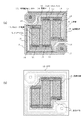
図1(a)〜(f)は本発明の熱型赤外線固体撮像素子の製造方法における主要工程を示す縦断面構造図であり、図2(a),(b)はそれぞれ庇を取り除いた状態と庇を設けた状態の単位画素平面図である。 1 (a) to 1 (f) are longitudinal sectional views showing main steps in the method for manufacturing a thermal infrared solid-state imaging device of the present invention, and FIGS. 2 (a) and 2 (b) are states in which wrinkles are removed, respectively. It is a unit pixel top view of the state which provided 庇 and 庇.
まず、通常のSi集積回路製造工程により、信号読出回路(図示せず),金属反射膜2,及び接続電極3を複数具備したSi集積回路基板1を形成する。図1(a)〜(f)には描かれていないが、Si集積回路基板1表面や金属反射膜2及び接続電極3を覆うように、全体に絶縁保護膜を形成しておいても良い。
First, the Si integrated
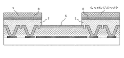
図1(a)において、支持部6と接続電極3との接触部を除いて、ダイアフラム5や支持部6とSi集積回路基板1との間の空隙を形成するための第1犠牲層4を、Si集積回路基板1上に形成する。第1犠牲層4は、例えば、感光性ポリイミドを塗布し、露光・現像によってパターニングした後、熱処理を施して形成する。第1犠牲層4の厚さは0.5〜3mm程度である。第1犠牲層4及び接続電極3上にダイアフラム5や支持部6を形成する。これらの形成は、まずプラズマCVD法等で下層絶縁保護膜を形成する。下層絶縁保護膜は、膜厚50〜500 nm程度のSi酸化膜(SiO,SiO2),Si窒化膜(SiN,Si3N4),あるいはSi酸化窒化膜(SiON)などから成る。その上にボロメータ薄膜13を構成する材料膜をスパッタ法等で形成し、図2(a)に示す画素のダイアフラム5に対応するようにボロメータ薄膜13のパターニングを行なう。例えば、ボロメータ薄膜13は、膜厚が50〜200 nm程度の酸化バナジウム(V2O3,VOXなど)や酸化チタン(TiOX)などから成る。ボロメータ薄膜13を覆う絶縁保護膜をプラズマCVD法等で形成し、該絶縁保護膜にボロメータコンタクト16及び接続電極コンタクト17を開口する。該絶縁保護膜は、膜厚50〜200 nm程度のSi酸化膜(SiO,SiO2),Si窒化膜(SiN,Si3N4),あるいはSi酸化窒化膜(SiON)などから成る。金属配線15を構成する金属薄膜をスパッタ法等で形成し、支持部6に対応するように金属配線15のパターニングを行なう。金属配線15は、膜厚が50〜200 nm程度のアルミニウム,銅,金,チタン,タングステン,モリブデン,あるいはチタン・アルミニウム・バナジウムなどから成る。さらにそれらの上を覆うようにプラズマCVD法等で上層絶縁保護膜を形成する。上層絶縁保護膜は、膜厚50〜500 nm程度のSi酸化膜(SiO,SiO2),Si窒化膜(SiN,Si3N4),あるいはSi酸化窒化膜(SiON)などから成る。最後に上層絶縁保護膜から下層絶縁保護膜までをまとめてダイアフラム5及び支持部6の形状になるようにパターニングして図2(a)の構造まで出来上がる。ダイアフラム5及び支持部6のパターニングには、同時に第1犠牲層4のポリイミドを部分的に露出させる効果もある。図1(a)では、さらに図2(a)の単位画素上全面に第2犠牲層7及び庇形成用第1層部材8を形成している。第2犠牲層7は、例えば、感光性ポリイミドを塗布し、露光・現像によって画素がアレイ状に配置された領域の周囲のみ除去するパターニングを行なった後、熱処理を施して形成する。第2犠牲層7の厚さは0.5〜3 mm程度である。庇形成用第1層部材8は、膜厚20〜2000 nm程度のSi酸化膜(SiO,SiO2),Si窒化膜(SiN,Si3N4),あるいはSi酸化窒化膜(SiON)などから成り、プラズマCVD法等で形成する。
In FIG. 1 (a), the first
図1(b)において、フォトレジストマスク9を用いて、ダイアフラム5のエッジ直近まで庇形成用第1層部材8及び第2犠牲層7をドライエッチング除去する。エッチング除去する領域が、極狭いギャップではなく、露光装置性能から見て遥かに広いので、高精度のパターニングができる。ダイアフラム5最上層の材料と庇形成用第1層部材8の材料として同一の物質を選択した場合には、本ドライエッチング除去がダイアフラム5に達する前に、該材料がほとんどエッチングされず、第2犠牲層7のみエッチングされるような選択比の高いエッチング条件に切替える必要がある。
In FIG. 1 (b), using a photoresist mask 9, the
図1(c)において、ダイアフラム5上の接続領域より内側に第3犠牲層10を形成する。第3犠牲層10は、例えば、感光性ポリイミドを塗布し、露光・現像によってパターニングした後、熱処理を施して形成する。ここでのパターニングも、露光装置性能から見て遥かに広い領域を除去するものなので、高精度で加工することができる。その結果できるダイアフラム5上の接続領域の幅は、露光装置性能限界を超える細さにすることもできる。本工程での感光性ポリイミド塗布時に、感光性ポリイミドから成る第2犠牲層7と接触する領域が存在するが、第2犠牲層7は先の熱処理により既に変質・硬化しているので、露光・現像時に第2犠牲層7の形状を崩すことは無くパターニングすることができる。第3犠牲層10の厚さは0.5〜3 mm程度である。
In FIG. 1C, the third
図1(d)において、庇形成用第1層部材8上、ダイアフラム5の接続領域上、及び、第3犠牲層10上に、庇形成用第2層部材11を形成する。庇形成用第2層部材11は、膜厚10〜500 nm程度のSi酸化膜(SiO,SiO2),Si窒化膜(SiN,Si3N4),あるいはSi酸化窒化膜(SiON)などから成り、プラズマCVD法等で形成する。
In FIG. 1D, the second layer member 11 for forming ridges is formed on the
図1(e)において、画素間を切離す、庇部12構造のパターニングを行なうが、このとき同時にダイアフラム5中央部の第3犠牲層10上の庇形成用第2層部材11不要部分もエッチング除去する。この結果、図2(b)に示すように、庇部12は極狭い帯状の庇接続部18によってダイアフラム5と接着し、その僅か内側にて庇開口部19が開けられている。庇形成用第2層部材11不要部分のエッチングが島状の第3犠牲層10内で終了し、庇開口部19内には第3犠牲層10が一部残った状態になっている。
In FIG. 1 (e), patterning of the
図1(f)において、第1犠牲層4、第2犠牲層7、及び、第3犠牲層10を、O2ガスプラズマを用いたアッシングにより除去することで、庇部12のSi集積回路基板1側の空隙と、ダイアフラム5のSi集積回路基板1側の空隙を形成すると共に、庇開口部19内も空にする。
In FIG. 1 (f), the first
以上の工程を経た結果、図1(f)に示すように、庇部が、ダイアフラム5以外の構成要素との間に空間を隔ててダイアフラム5以外の構成要素の基板と反対側の面を覆う部位の膜が2層で厚く、庇接続部及びダイアフラム5から空中に立ち上がる部位の膜が1層で薄い構造を有し、尚且つ、ダイアフラムエッジから庇接続部までのマージン及び庇接続部から庇開口部までのマージンが極小さい熱型赤外線検出器を複数配列した熱型赤外線固体撮像素子が実現できる。当該熱型赤外線固体撮像素子の特徴により、入射赤外線吸収力を維持乃至向上させつつ、画素の熱応答特性改善を達成できている。
As a result of the above steps, as shown in FIG. 1 (f), the flange portion covers the surface opposite to the substrate of the components other than the
上述した実施の形態において、図1(a)で庇形成用部材を1層しか形成しなかったが、ここで任意の層数の膜を形成すれば、庇部に赤外線の吸収や透過の特殊な波長特性を持たせた熱型赤外線固体撮像素子を実現することができる。赤外線入射側最外膜を導電性の材質とし、さらに空間とインピーダンス整合(シート抵抗条件 377 W/□)を取ることにより、入射赤外線の反射損失を低減することもできる。 In the above-described embodiment, only one layer of the ridge-forming member is formed in FIG. 1 (a), but if a film having an arbitrary number of layers is formed here, special absorption or transmission of infrared rays is formed in the heel portion. Therefore, it is possible to realize a thermal infrared solid-state imaging device having a special wavelength characteristic. By making the outermost film on the infrared incident side into a conductive material and further matching the impedance with the space (sheet resistance condition 377 W / □), the reflection loss of incident infrared radiation can be reduced.
また、図1(d)でも庇形成用部材を1層しか形成しなかったが、これも多層にしてそれら多種の物質の相乗効果により機械的強度を増し、全体の膜厚をさらに減少させることもできる。 In FIG. 1 (d), only one layer of wrinkle-forming members was formed, but this was also made multilayered to increase the mechanical strength due to the synergistic effect of these various substances and further reduce the overall film thickness. You can also.
加えて、第1犠牲層4、第2犠牲層7、及び、第3犠牲層10をポリシリコンやアルミニウムで構成することができる。第2犠牲層7と第3犠牲層10を同種の材料で構成する場合、図1(c)における第3犠牲層10のパターニングに異方性の強いドライエッチングを用いるのであれば問題無いが、そうでない場合には第2犠牲層7の側壁形状が崩れる危険があるので、図3(a)〜(c)に示すように、第3犠牲層10形成前に極薄い犠牲層保護膜20を形成する。ポリシリコンを犠牲層に用いる場合の犠牲層除去は、例えば、ヒドラジンやテトラメチルアンモニウムハイドロオキサイド(TMAH)を用いたウェットエッチング、XeF2プラズマを用いたドライエッチング等により行なう。アルミニウムを犠牲層に用いる場合の犠牲層除去は、例えば、塩酸やホットリン酸を用いたウェットエッチングにより行なう。なお、ダイアフラム5や支持部6を構成する絶縁保護膜にSi窒化膜を用いた場合には、ホットリン酸をあまり高温(〜160℃)にするとSi窒化膜もエッチングされるので注意が必要である。
In addition, the first
また、ダイアフラム5、支持部6、及び、庇部12を構成する材料にSi酸化膜を用いる場合には、第1犠牲層4、第2犠牲層7、及び、第3犠牲層10をSi窒化膜で構成することも可能であり、さらに、その逆も可能である。Si窒化膜が犠牲層の場合の犠牲層除去は、例えば、ホットリン酸を用いたウェットエッチングで行ない、Si酸化膜が犠牲層の場合の犠牲層除去は、例えば、弗酸を用いたウェットエッチングで行なう。
In the case where a Si oxide film is used as the material constituting the
上述した実施の形態では、温度検出部としてボロメータ薄膜を備えたボロメータ型赤外線固体撮像素子について述べたが、本発明はこれに限定されず、例えば温度検出部としてサーモパイルを備えたものなど庇構造によって高感度化できる熱型赤外線固体撮像素子において全て効果を発揮し得るものである。 In the above-described embodiment, the bolometer-type infrared solid-state imaging device provided with the bolometer thin film as the temperature detection unit has been described. However, the present invention is not limited to this, and for example, by a saddle structure such as one provided with a thermopile as the temperature detection unit. All effects can be achieved in a thermal infrared solid-state imaging device capable of increasing sensitivity.
有効画素数320×240で画素ピッチ23.5 mmのボロメータ型赤外線固体撮像素子を製作した。Si集積回路基板上に、図2に示す構造の画素をアレイ状に形成しており、画素全面積に対するダイアフラム面積の割合は庇構造を持たない(a)の場合で約60%、庇構造を持つ(b)の場合で約92%となった。ダイアフラム及び支持部を構成する下層絶縁保護膜と上層絶縁保護膜とは共に膜厚150 nmのSi窒化膜で形成した。ボロメータ薄膜としては、膜厚100 nmの酸化バナジウムを用いた。ボロメータ薄膜上の絶縁保護膜には膜厚50 nmのSi窒化膜を用いた。配線には赤外線で生じた熱をできるだけ逃がさないようにするため、熱伝導率の低い膜厚50 nmのチタン・アルミニウム・バナジウムを採用した。庇部は、庇形成用第1層部材を膜厚250 nmのSi窒化膜、庇形成用第2層部材を膜厚50 nmのSi窒化膜で形成した。ダイアフラムエッジから庇接続部までのマージンを0.3 mm、接続部幅を0.4 mm、庇接続部から庇開口部までのマージンを0.4 mmとした。その結果、画素受光面積に対する庇開口部面積の割合は、約49%であった。 A bolometer-type infrared solid-state imaging device with 320 × 240 effective pixels and a pixel pitch of 23.5 mm was manufactured. Pixels with the structure shown in FIG. 2 are formed in an array on a Si integrated circuit substrate, and the ratio of the diaphragm area to the total area of the pixels is about 60% in the case of (a) without the ridge structure. In case of (b), it was about 92%. The lower insulating protective film and the upper insulating protective film constituting the diaphragm and the support part were both formed of a 150 nm-thickness Si nitride film. As the bolometer thin film, vanadium oxide having a film thickness of 100 nm was used. A 50-nm-thick Si nitride film was used as the insulating protective film on the bolometer thin film. To prevent the heat generated by infrared rays from escaping as much as possible, 50 nm thick titanium, aluminum, and vanadium with low thermal conductivity were used for the wiring. For the heel part, the first layer member for ridge formation was formed with a Si nitride film with a thickness of 250 nm, and the second layer member for ridge formation was formed with a Si nitride film with a thickness of 50 nm. The margin from the diaphragm edge to the heel connection was 0.3 mm, the connection width was 0.4 mm, and the margin from the heel connection to the heel opening was 0.4 mm. As a result, the ratio of the heel opening area to the pixel light receiving area was about 49%.
図6に示す従来構造の画素を有する同規格のボロメータ型赤外線固体撮像素子も同時に製作して前述のものと性能比較を行なった。庇部は膜厚300 nmのSi窒化膜で形成した。ダイアフラムエッジから庇接続部までのマージンは1 mm、接続部幅は1 mm、庇接続部から庇開口部までのマージンは0.75 mmとなった。その結果、画素受光面積に対する庇開口部面積の割合は、約27%となった。このことから、本発明では、庇形成用部材不要部分除去率が約1.8倍に改善されていることがわかる。 A bolometer-type infrared solid-state image sensor of the same standard having a pixel with the conventional structure shown in FIG. 6 was manufactured at the same time, and its performance was compared with that described above. The buttocks were made of Si nitride film with a film thickness of 300 nm. The margin from the diaphragm edge to the heel connection was 1 mm, the connection width was 1 mm, and the margin from the heel connection to the heel opening was 0.75 mm. As a result, the ratio of the heel opening area to the pixel light receiving area was about 27%. From this, it can be seen that in the present invention, the removal rate of the unnecessary part for forming the wrinkle is improved by about 1.8 times.
庇部の受光部分については、両者の材質及び膜厚が同一なので、感度比較では同等性能であった。しかしながら、熱時定数を比較したところ、本発明における画素の体積が従来のものの約75%に削減されたため、従来の約16 msecに対して本発明では約12 msecの熱時定数を得ることができた。 As for the light receiving portion of the collar portion, the material and the film thickness are the same. However, when comparing the thermal time constant, the pixel volume in the present invention was reduced to about 75% of the conventional one, so that the present invention can obtain a thermal time constant of about 12 msec compared to the conventional about 16 msec. did it.
以上により、本発明の熱型赤外線固体撮像素子及びその製造方法の有効性が確認された。 As described above, the effectiveness of the thermal infrared solid-state imaging device and the manufacturing method thereof of the present invention was confirmed.
本発明の活用例として、暗視装置(赤外線カメラ)やサーモグラフィに使用される熱型赤外線固体撮像素子の製造が挙げられる。 As an application example of the present invention, the manufacture of a thermal infrared solid-state imaging device used in night vision devices (infrared cameras) and thermography can be mentioned.
1 Si集積回路基板
2 金属反射膜
3 接続電極
4 第1犠牲層
5 ダイアフラム
6 支持部
6a 梁
6b 支持脚
7 第2犠牲層
8 庇形成用第1層部材
9 フォトレジストマスク
10 第3犠牲層
11 庇形成用第2層部材
12 庇部
13 ボロメータ薄膜
14 電極部
15 金属配線
16 ボロメータコンタクト
17 接続電極コンタクト
18 庇接続部
19 庇開口部
20 犠牲層保護膜
21 第1絶縁保護膜
22 赤外線受光部
23 空洞部
24 第2絶縁保護膜
25 第3絶縁保護膜
26 第4絶縁保護膜
27 信号読出回路
DESCRIPTION OF
Claims (12)
前記ダイアフラムの外周近傍に接続され、該外周近傍から空中に立ち上がり、前記ダイアフラムの外側に延びる庇部を備え、
前記庇部は、前記ダイアフラムの外側に延びる第1の部位が、前記ダイアフラムの外周近傍に接続される第2の部位及び該外周近傍から空中に立ち上がる第3の部位よりも、厚く形成されていることを特徴とする熱型赤外線固体撮像素子。 An infrared detecting element in which a diaphragm including a temperature detecting unit connected to the wiring is supported in a floating state from the substrate by a supporting unit including wiring connected to an integrated circuit for signal readout formed on the substrate In a thermal infrared solid-state imaging device in which a plurality of are arranged,
Connected to the vicinity of the outer periphery of the diaphragm, rising in the air from the vicinity of the outer periphery, and having a flange extending to the outside of the diaphragm,
In the flange portion, the first part extending outside the diaphragm is formed thicker than the second part connected to the vicinity of the outer periphery of the diaphragm and the third part rising in the air from the vicinity of the outer periphery. A thermal infrared solid-state imaging device characterized by the above.
赤外線を吸収することにより加熱される赤外線吸収部、該赤外線吸収部からの熱によって温度が変化して前記赤外線吸収部の温度変化を検出する温度検出部、及び、該温度検出部と電気的に接続された電極部を備え、前記基板の一側の面上に間隔を空けて配置されるダイアフラムと、
前記ダイアフラムを前記基板の前記一側の面から浮かせて支持し、前記基板の前記接続電極に前記ダイアフラムの前記電極部を電気的に接続する配線を構成するように少なくとも一部が導電性材料により形成された支持部と、を少なくとも有する赤外線検出素子が複数配置された熱型赤外線固体撮像素子において、
前記ダイアフラムの外周近傍に設けられる接続領域に接続され、少なくとも前記ダイアフラム以外の構成要素との間に空間を隔てて前記ダイアフラム以外の構成要素の基板と反対側の面を覆い、入射する赤外線を吸収して発生する熱を前記ダイアフラムに伝達する庇部を備え、
前記庇部は、少なくとも前記ダイアフラム以外の構成要素との間に空間を隔てて前記ダイアフラム以外の構成要素の基板と反対側の面を覆う第1の部位の厚さが、前記ダイアフラムの接続領域に接している第2の部位及び前記ダイアフラムから空中に立ち上がる第3の部位の厚さよりも厚いことを特徴とする熱型赤外線固体撮像素子。 An integrated circuit for signal readout is formed, and a substrate having connection electrodes with the integrated circuit;
An infrared absorbing portion heated by absorbing infrared rays, a temperature detecting portion for detecting a temperature change of the infrared absorbing portion due to a change in temperature by heat from the infrared absorbing portion, and electrically with the temperature detecting portion A diaphragm comprising a connected electrode portion, and disposed on a surface of one side of the substrate with a space therebetween;
The diaphragm is supported by being floated from the one side surface of the substrate, and at least a part thereof is made of a conductive material so as to constitute a wiring that electrically connects the electrode portion of the diaphragm to the connection electrode of the substrate. In the thermal infrared solid-state imaging device in which a plurality of infrared detection elements having at least a formed support portion are arranged,
It is connected to a connection region provided near the outer periphery of the diaphragm, covers at least a component other than the diaphragm, covers a surface opposite to the substrate of the component other than the diaphragm, and absorbs incident infrared rays. A flange that transmits heat generated to the diaphragm;
The collar has a thickness of a first portion that covers a surface opposite to the substrate of a component other than the diaphragm with a space between at least a component other than the diaphragm, in a connection region of the diaphragm. A thermal infrared solid-state imaging device, characterized in that it is thicker than the thickness of the second part in contact and the third part that rises in the air from the diaphragm.
前記第1の犠牲層上に、温度検出部を含むダイアフラムを形成すると共に、一端が前記接続電極に接続され、他端が前記温度検出部に接続される配線を含む支持部を形成し、その際、前記ダイアフラム及び前記支持部を形造るために開口する第1スリットにより、前記第1の犠牲層を露出させる第2の工程と、
前記基板全面に、第2の犠牲層を配設し、該第2の犠牲層上に、庇形成用第1の部材を配設する第3の工程と、
前記ダイアフラム上の前記庇形成用第1の部材及び前記第2の犠牲層をパターニング除去する第4の工程と、
前記ダイアフラム上に、外周近傍を除いて、第3の犠牲層を配設する第5の工程と、
前記基板全面に、庇形成用第2の部材を配設する第6の工程と、
前記ダイアフラムの外周近傍よりも内側に配設された庇形成用第2の部材をパターニング除去すると共に、前記ダイアフラムの外周近傍よりも外側に配設された前記庇形成用第2の部材及び前記庇形成用第1部材の一部をパターニング除去して前記第2の犠牲層を露出させる第2スリットを形成する第7の工程と、
前記ダイアフラム上の前記第3の犠牲層を除去すると共に、前記第2スリット及び前記第1スリットを介して、前記基板上の前記第2の犠牲層及び前記第1の犠牲層を除去する第8の工程と、
を少なくとも有することを特徴とする熱型赤外線固体撮像素子の製造方法。 A first step of forming an integrated circuit for signal readout and disposing a first sacrificial layer on a substrate having a connection electrode with the integrated circuit except for the connection electrode;
On the first sacrificial layer, a diaphragm including a temperature detection unit is formed, and a support unit including a wiring having one end connected to the connection electrode and the other end connected to the temperature detection unit is formed. A second step of exposing the first sacrificial layer by a first slit opened to shape the diaphragm and the support;
A third step of disposing a second sacrificial layer over the entire surface of the substrate, and disposing a first member for forming a ridge on the second sacrificial layer;
A fourth step of patterning and removing the first member for wrinkle formation and the second sacrificial layer on the diaphragm;
A fifth step of disposing a third sacrificial layer on the diaphragm except for the vicinity of the outer periphery;
A sixth step of disposing a second member for wrinkle formation on the entire surface of the substrate;
The second member for forming wrinkles disposed inside the vicinity of the outer periphery of the diaphragm is removed by patterning, and the second member for forming wrinkles disposed outside the vicinity of the outer periphery of the diaphragm and the wrinkles A seventh step of patterning and removing a part of the first forming member to form a second slit exposing the second sacrificial layer;
Removing the third sacrificial layer on the diaphragm and removing the second sacrificial layer and the first sacrificial layer on the substrate via the second slit and the first slit; And the process of
A method for producing a thermal-type infrared solid-state imaging device, comprising:
前記第1の犠牲層上に、赤外線を吸収することにより加熱される赤外線吸収部、該赤外線吸収部からの熱によって温度が変化して前記赤外線吸収部の温度変化を検出する温度検出部、及び、該温度検出部と電気的に接続される電極部を備えるダイアフラムを形成すると共に、前記ダイアフラムの外側の前記接続電極上及び前記第1の犠牲層上に、該ダイアフラムを前記基板の一側の面から浮かせて支持し、前記基板の前記接続電極に前記ダイアフラムの前記電極部を電気的に接続する配線を構成するように少なくとも一部が導電性材料により形成される支持部を形成する第2の工程と、
前記基板上の赤外線検出素子形成領域全面に、第2の犠牲層を配設し、加えて該第2の犠牲層上に庇形成用第1の部材を配設する第3の工程と、
前記ダイアフラム上の外周近傍に設けられる庇部の接続領域及び該接続領域から内側の領域に存在する、前記庇形成用第1の部材及び前記第2の犠牲層をパターニング除去する第4の工程と、
前記ダイアフラム上における前記庇形成用第1の部材及び前記第2の犠牲層が除去された領域上に、前記ダイアフラム上の外周近傍に設けられる前記接続領域を除いて、第3の犠牲層を配設する第5の工程と、
前記庇形成用第1の部材上、前記接続領域上、及び、前記第3の犠牲層上に、庇形成用第2の部材を配設する第6の工程と、
前記接続領域外側における一部領域の、前記庇形成用第2の部材及び前記庇形成用第1部材をパターニング除去すると共に、前記第3の犠牲層上の開口部となる領域の前記庇形成用第1の部材をパターニング除去して、庇部を形成する第7の工程と、
前記庇形成用第1の部材及び前記庇形成用第2の部材を除去した領域から、前記第1の犠牲層、前記第2の犠牲層、及び、前記第3の犠牲層を除去する第8の工程と、
を少なくとも有することを特徴とする熱型赤外線固体撮像素子の製造方法。 A first step of forming an integrated circuit for signal readout and disposing a first sacrificial layer on a substrate having a connection electrode with the integrated circuit except for the connection electrode;
On the first sacrificial layer, an infrared absorption part heated by absorbing infrared rays, a temperature detection part for detecting a temperature change of the infrared absorption part by changing the temperature by heat from the infrared absorption part, and Forming a diaphragm having an electrode portion electrically connected to the temperature detection portion, and placing the diaphragm on one side of the substrate on the connection electrode and the first sacrificial layer outside the diaphragm. A second support portion that is supported by being floated from a surface, and at least part of which is formed of a conductive material so as to form a wiring that electrically connects the electrode portion of the diaphragm to the connection electrode of the substrate. And the process of
A third step of disposing a second sacrificial layer on the entire surface of the infrared detection element forming region on the substrate, and additionally disposing a first member for forming a ridge on the second sacrificial layer;
A fourth step of patterning and removing the first member for forming heels and the second sacrificial layer existing in the inner region from the connection region of the heel portion provided near the outer periphery on the diaphragm and the connection region; ,
On the diaphragm, a third sacrificial layer is arranged on the area where the first member for wrinkle formation and the second sacrificial layer are removed, except for the connection region provided in the vicinity of the outer periphery on the diaphragm. A fifth step to be established;
A sixth step of disposing a second member for wrinkle formation on the first member for wrinkle formation, on the connection region, and on the third sacrificial layer;
For patterning removal of the second member for forming wrinkles and the first member for forming wrinkles in a partial region outside the connection region, and for forming the wrinkles in a region to be an opening on the third sacrificial layer A seventh step of patterning and removing the first member to form a collar;
Eighth removing the first sacrificial layer, the second sacrificial layer, and the third sacrificial layer from the region where the first member for forming wrinkles and the second member for forming wrinkles are removed. And the process of
A method for producing a thermal-type infrared solid-state imaging device, comprising:
前記ダイアフラム上、前記庇形成用第1の部材上、及び、パターニング除去によって形成された前記第2の犠牲層側壁上に、犠牲層保護膜を配設する工程を加えたことを特徴とする請求項8又は9に記載の熱型赤外線固体撮像素子の製造方法。 After the fourth step,
A step of disposing a sacrificial layer protective film on the diaphragm, the first member for forming the ridge, and the side wall of the second sacrificial layer formed by patterning removal is added. Item 10. A method for producing a thermal infrared solid-state imaging device according to Item 8 or 9.
Priority Applications (4)
| Application Number | Priority Date | Filing Date | Title |
|---|---|---|---|
| JP2008086526A JP4697611B2 (en) | 2008-03-28 | 2008-03-28 | Thermal infrared solid-state imaging device and manufacturing method thereof |
| EP09004401A EP2105719A1 (en) | 2008-03-28 | 2009-03-26 | Thermal-type infrared solid-state imaging device and manufacturing method of the same |
| US12/412,708 US8101914B2 (en) | 2008-03-28 | 2009-03-27 | Thermal-type infrared solid-state imaging device and manufacturing method of the same |
| CN200910130257A CN101545809A (en) | 2008-03-28 | 2009-03-30 | Thermal-type infrared solid-state imaging device and manufacturing method of the same |
Applications Claiming Priority (1)
| Application Number | Priority Date | Filing Date | Title |
|---|---|---|---|
| JP2008086526A JP4697611B2 (en) | 2008-03-28 | 2008-03-28 | Thermal infrared solid-state imaging device and manufacturing method thereof |
Publications (2)
| Publication Number | Publication Date |
|---|---|
| JP2009236865A true JP2009236865A (en) | 2009-10-15 |
| JP4697611B2 JP4697611B2 (en) | 2011-06-08 |
Family
ID=40640229
Family Applications (1)
| Application Number | Title | Priority Date | Filing Date |
|---|---|---|---|
| JP2008086526A Active JP4697611B2 (en) | 2008-03-28 | 2008-03-28 | Thermal infrared solid-state imaging device and manufacturing method thereof |
Country Status (4)
| Country | Link |
|---|---|
| US (1) | US8101914B2 (en) |
| EP (1) | EP2105719A1 (en) |
| JP (1) | JP4697611B2 (en) |
| CN (1) | CN101545809A (en) |
Cited By (2)
| Publication number | Priority date | Publication date | Assignee | Title |
|---|---|---|---|---|
| US9105368B2 (en) | 2012-05-09 | 2015-08-11 | Panasonic Intellectual Property Management Co., Ltd. | Infrared radiation element |
| JP2018197713A (en) * | 2017-05-24 | 2018-12-13 | 三菱電機株式会社 | Infrared sensor and infrared solid-state imaging device |
Families Citing this family (7)
| Publication number | Priority date | Publication date | Assignee | Title |
|---|---|---|---|---|
| JP2011153871A (en) * | 2010-01-26 | 2011-08-11 | Seiko Epson Corp | Thermal photodetector, thermal photodetecting device, and electronic instrument |
| JP5589605B2 (en) * | 2010-06-25 | 2014-09-17 | セイコーエプソン株式会社 | Pyroelectric detector, pyroelectric detector and electronic device |
| US8890264B2 (en) * | 2012-09-26 | 2014-11-18 | Intel Corporation | Non-planar III-V field effect transistors with conformal metal gate electrode and nitrogen doping of gate dielectric interface |
| US9297700B2 (en) | 2012-12-03 | 2016-03-29 | Analog Devices, Inc. | Photonic sensor and a method of manufacturing such a sensor |
| CN105712284B (en) | 2014-12-02 | 2017-09-29 | 无锡华润上华半导体有限公司 | The preparation method and MEMS infrared detectors of MEMS Double-layered suspended micro-structurals |
| CN108351254B (en) * | 2016-09-02 | 2021-10-22 | 索尼半导体解决方案公司 | Image pickup apparatus |
| CN106276781B (en) * | 2016-09-06 | 2017-10-17 | 烟台睿创微纳技术股份有限公司 | A kind of micro-metering bolometer refers to the preparation method and structure of pixel |
Citations (4)
| Publication number | Priority date | Publication date | Assignee | Title |
|---|---|---|---|---|
| JP2001215151A (en) * | 2000-01-31 | 2001-08-10 | Nec Corp | Thermal infrared detector and its manufacturing method |
| JP2004317152A (en) * | 2003-04-11 | 2004-11-11 | Mitsubishi Electric Corp | Thermal type infrared detector and infrared focal plane array |
| JP2005116856A (en) * | 2003-10-09 | 2005-04-28 | Nec Corp | Thermal infrared solid-state imaging device and its manufacturing method |
| JP2009192350A (en) * | 2008-02-14 | 2009-08-27 | Nec Corp | Thermal type infrared detector and manufacturing method therefor |
Family Cites Families (5)
| Publication number | Priority date | Publication date | Assignee | Title |
|---|---|---|---|---|
| JP3040356B2 (en) * | 1997-01-27 | 2000-05-15 | 三菱電機株式会社 | Infrared solid-state imaging device |
| JP3409848B2 (en) * | 2000-08-29 | 2003-05-26 | 日本電気株式会社 | Thermal infrared detector |
| JP3862080B2 (en) * | 2002-11-01 | 2006-12-27 | 防衛庁技術研究本部長 | Method for manufacturing thermal infrared detector |
| JP2008086526A (en) | 2006-09-29 | 2008-04-17 | Pentax Corp | Autoclave sterilization method |
| JP5251310B2 (en) * | 2008-07-08 | 2013-07-31 | 日本電気株式会社 | Two-wavelength thermal infrared array sensor |
-
2008
- 2008-03-28 JP JP2008086526A patent/JP4697611B2/en active Active
-
2009
- 2009-03-26 EP EP09004401A patent/EP2105719A1/en not_active Withdrawn
- 2009-03-27 US US12/412,708 patent/US8101914B2/en active Active
- 2009-03-30 CN CN200910130257A patent/CN101545809A/en active Pending
Patent Citations (4)
| Publication number | Priority date | Publication date | Assignee | Title |
|---|---|---|---|---|
| JP2001215151A (en) * | 2000-01-31 | 2001-08-10 | Nec Corp | Thermal infrared detector and its manufacturing method |
| JP2004317152A (en) * | 2003-04-11 | 2004-11-11 | Mitsubishi Electric Corp | Thermal type infrared detector and infrared focal plane array |
| JP2005116856A (en) * | 2003-10-09 | 2005-04-28 | Nec Corp | Thermal infrared solid-state imaging device and its manufacturing method |
| JP2009192350A (en) * | 2008-02-14 | 2009-08-27 | Nec Corp | Thermal type infrared detector and manufacturing method therefor |
Cited By (2)
| Publication number | Priority date | Publication date | Assignee | Title |
|---|---|---|---|---|
| US9105368B2 (en) | 2012-05-09 | 2015-08-11 | Panasonic Intellectual Property Management Co., Ltd. | Infrared radiation element |
| JP2018197713A (en) * | 2017-05-24 | 2018-12-13 | 三菱電機株式会社 | Infrared sensor and infrared solid-state imaging device |
Also Published As
| Publication number | Publication date |
|---|---|
| US20090242768A1 (en) | 2009-10-01 |
| EP2105719A1 (en) | 2009-09-30 |
| CN101545809A (en) | 2009-09-30 |
| JP4697611B2 (en) | 2011-06-08 |
| US8101914B2 (en) | 2012-01-24 |
Similar Documents
| Publication | Publication Date | Title |
|---|---|---|
| JP4697611B2 (en) | Thermal infrared solid-state imaging device and manufacturing method thereof | |
| JP3862080B2 (en) | Method for manufacturing thermal infrared detector | |
| JP3921320B2 (en) | Thermal infrared detector and method for manufacturing the same | |
| JP5597862B2 (en) | Bolometer type THz wave detector | |
| EP0859413B1 (en) | Infrared focal plane array | |
| JP3514681B2 (en) | Infrared detector | |
| US8541742B2 (en) | Bolometer-type THz wave detector | |
| US8618483B2 (en) | Bolometer type Terahertz wave detector | |
| US8350350B2 (en) | Optical sensor | |
| US7667202B2 (en) | Multilayer-structured bolometer and method of fabricating the same | |
| JP2008241439A (en) | Bolometer type thz wave detector | |
| US7276698B2 (en) | Thermal-type infra-red ray solid-state image sensor and method of fabricating the same | |
| JP2009192350A (en) | Thermal type infrared detector and manufacturing method therefor | |
| TWI457547B (en) | Photodetector | |
| JP2005043381A (en) | Thermal type infrared detector and its manufacturing method | |
| JP5708122B2 (en) | Thermal infrared solid-state imaging device and manufacturing method thereof | |
| US20110198720A1 (en) | Thermal-type infrared solid-state imaging element | |
| JP3574368B2 (en) | Infrared solid-state imaging device | |
| JP2010101675A (en) | Infrared imaging element and method of manufacturing the same | |
| US5607600A (en) | Optical coat reticulation post hybridization | |
| KR20090103842A (en) | Thermal-type infrared solid-state imaging device and manufacturing method of the same | |
| JP2000346704A (en) | Bolometer type infrared detection element | |
| JP2012127881A (en) | Infrared sensor and infrared sensor array |
Legal Events
| Date | Code | Title | Description |
|---|---|---|---|
| A977 | Report on retrieval |
Free format text: JAPANESE INTERMEDIATE CODE: A971007 Effective date: 20091224 |
|
| A131 | Notification of reasons for refusal |
Free format text: JAPANESE INTERMEDIATE CODE: A131 Effective date: 20100205 |
|
| A521 | Written amendment |
Free format text: JAPANESE INTERMEDIATE CODE: A523 Effective date: 20100308 |
|
| A131 | Notification of reasons for refusal |
Free format text: JAPANESE INTERMEDIATE CODE: A131 Effective date: 20100803 |
|
| A521 | Written amendment |
Free format text: JAPANESE INTERMEDIATE CODE: A523 Effective date: 20100930 |
|
| TRDD | Decision of grant or rejection written | ||
| A01 | Written decision to grant a patent or to grant a registration (utility model) |
Free format text: JAPANESE INTERMEDIATE CODE: A01 Effective date: 20110204 |
|
| A61 | First payment of annual fees (during grant procedure) |
Free format text: JAPANESE INTERMEDIATE CODE: A61 Effective date: 20110217 |
|
| R150 | Certificate of patent or registration of utility model |
Ref document number: 4697611 Country of ref document: JP Free format text: JAPANESE INTERMEDIATE CODE: R150 |