JP2009226504A - Wire electric discharge machining device - Google Patents
Wire electric discharge machining device Download PDFInfo
- Publication number
- JP2009226504A JP2009226504A JP2008071828A JP2008071828A JP2009226504A JP 2009226504 A JP2009226504 A JP 2009226504A JP 2008071828 A JP2008071828 A JP 2008071828A JP 2008071828 A JP2008071828 A JP 2008071828A JP 2009226504 A JP2009226504 A JP 2009226504A
- Authority
- JP
- Japan
- Prior art keywords
- pulse
- wire
- voltage
- electric discharge
- discharge machining
- Prior art date
- Legal status (The legal status is an assumption and is not a legal conclusion. Google has not performed a legal analysis and makes no representation as to the accuracy of the status listed.)
- Pending
Links
Images


Landscapes
- Electrical Discharge Machining, Electrochemical Machining, And Combined Machining (AREA)
Abstract
Description
この発明は、被加工物とワイヤとの間で放電を生じさせることにより、例えば被加工物の一部除去や切断等の放電加工を行うワイヤ放電加工装置に関する。 The present invention relates to a wire electric discharge machining apparatus that performs electric discharge machining such as partial removal or cutting of a workpiece, for example, by generating electric discharge between the workpiece and a wire.
従来の放電式ワイヤソーは、被加工物(ワーク)と各ワイヤ(切断ワイヤ部分)との間の放電電圧を検出し、各電圧検出値に基づいて、被加工物の切断送り動作、すなわち被加工物の位置を制御している(例えば、特許文献1参照)。
具体的には、各電圧検出値のうちの最小値があらかじめ設定された目標値よりも低くなった場合に、被加工物の切断送りが停止される。また、この最小値が目標値よりも高い場合には、この最小値と目標値との差に応じた速度で被加工物の切断送りが行われる。
A conventional electric discharge type wire saw detects a discharge voltage between a workpiece (workpiece) and each wire (cutting wire portion), and based on each voltage detection value, the workpiece is cut and fed, that is, the workpiece is processed. The position of the object is controlled (for example, refer to Patent Document 1).
Specifically, when the minimum value among the detected voltage values is lower than a preset target value, the cutting and feeding of the workpiece is stopped. If the minimum value is higher than the target value, the workpiece is cut and fed at a speed corresponding to the difference between the minimum value and the target value.
なお、電圧検出値が低下する原因としては、例えば以下の2つのものが考えられる。第1の原因としては、被加工物の切断送り速度が放電加工の加工速度よりも速く、被加工物とワイヤとが接近するものが考えられる。また、第2の原因としては、ワイヤの振動、または被加工物とワイヤとの間に加工屑等が挟まることにより短時間の短絡が発生し、加工状態が一時的に悪化するものが考えられる。 In addition, the following two things can be considered as a cause that a voltage detection value falls, for example. As the first cause, it can be considered that the cutting feed speed of the workpiece is faster than the machining speed of the electric discharge machining, and the workpiece and the wire approach each other. Further, as a second cause, it is conceivable that a short-circuit occurs for a short time due to vibration of the wire, or processing scraps are sandwiched between the workpiece and the wire, and the processing state temporarily deteriorates. .
しかしながら、従来技術には、次のような問題点があった。
すなわち、この充電式ワイヤソーでは、ワークと切断ワイヤ部分との相対的な位置関係を、ワークの切断送りを制御することにより機械的に制御している。そのため、ワークの切断送りの制御を行うことができる周波数帯域は、一般的に数十Hz以下の帯域に限定される。
これに対して、放電加工は、電気的な現象であり、数十kHz〜1MHz程度の周波数帯域で発生する。
However, the prior art has the following problems.
That is, in this rechargeable wire saw, the relative positional relationship between the workpiece and the cutting wire portion is mechanically controlled by controlling the cutting feed of the workpiece. For this reason, the frequency band in which the workpiece cutting and feeding can be controlled is generally limited to a band of several tens of Hz or less.
In contrast, electric discharge machining is an electrical phenomenon and occurs in a frequency band of about several tens of kHz to 1 MHz.
したがって、加工状態が一時的に悪化した場合には、ワークの切断送りの制御が開始されたときに、加工状態が既に改善していることが考えられる。そのため、適切なタイミングで放電加工の加工制御を行うことができず、短絡電流によりワイヤの切断が発生する恐れがあるという問題点があった。 Therefore, if the machining state temporarily deteriorates, it is considered that the machining state has already improved when the workpiece cutting and feeding control is started. For this reason, there is a problem in that electric discharge machining control cannot be performed at an appropriate timing, and the wire may be cut by a short-circuit current.
この発明は、上記のような課題を解決するためになされたものであって、その目的は、放電加工の加工状態が一時的に悪化した場合であっても、適切なタイミングで放電加工の加工制御を行い、ワイヤの断線を防止することができるワイヤ放電加工装置を提供することにある。 The present invention has been made to solve the above-described problems, and its purpose is to perform electrical discharge machining at an appropriate timing even when the electrical discharge machining state is temporarily deteriorated. An object of the present invention is to provide a wire electric discharge machining apparatus capable of performing control and preventing wire breakage.
この発明に係るワイヤ放電加工装置は、被加工物と対向する対向部で放電を生じさせることにより、被加工物を放電加工するワイヤと、被加工物とワイヤとの間にパルス電圧を印加するためのパルス電圧信号を生成するパルス生成手段と、パルス生成手段に直流電力を供給する電源手段と、被加工物とワイヤとの間の電圧を検出する電圧検出手段と、電圧検出手段で検出された電圧検出値に基づいてパルス電圧信号の信号波形を設定し、信号波形に対応したパルス波形信号をパルス生成手段に出力するパルス波形設定手段とを備え、パルス波形設定手段は、電圧検出値の絶対値が所定電圧値よりも低い場合に、放電加工の加工エネルギが低下するように信号波形を設定するものである。 The wire electric discharge machining apparatus according to the present invention applies a pulse voltage between a wire for electric discharge machining the workpiece and the workpiece and the wire by generating an electric discharge at a facing portion facing the workpiece. Detected by a pulse generation means for generating a pulse voltage signal, a power supply means for supplying DC power to the pulse generation means, a voltage detection means for detecting a voltage between the workpiece and the wire, and a voltage detection means A pulse waveform setting means for setting a signal waveform of the pulse voltage signal based on the detected voltage value and outputting a pulse waveform signal corresponding to the signal waveform to the pulse generating means. When the absolute value is lower than a predetermined voltage value, the signal waveform is set so that the machining energy of electric discharge machining is reduced.
この発明のワイヤ放電加工装置によれば、制御可能な周波数帯域の低い機械的制御に代えて、高い周波数帯域で制御可能な電気的制御を行うことにより、放電加工の加工制御を高速に行う。
具体的には、パルス波形設定手段は、電圧検出手段で検出された電圧検出値の絶対値が所定電圧値よりも低い場合に、放電加工の加工エネルギが低下するようにパルス電圧信号の信号波形を設定する。
そのため、放電加工の加工状態が一時的に悪化した場合であっても、適切なタイミングで放電加工の加工制御を行い、ワイヤの断線を防止することができる。
According to the wire electric discharge machining apparatus of the present invention, machining control of electric discharge machining is performed at high speed by performing electrical control that can be controlled in a high frequency band instead of mechanical control in a low frequency band that can be controlled.
Specifically, the pulse waveform setting means is configured to detect the signal waveform of the pulse voltage signal so that the machining energy of the electric discharge machining is reduced when the absolute value of the voltage detection value detected by the voltage detection means is lower than a predetermined voltage value. Set.
Therefore, even if the machining state of the electric discharge machining is temporarily deteriorated, the electric discharge machining control can be performed at an appropriate timing to prevent the wire from being disconnected.
以下、この発明の各実施の形態について図に基づいて説明するが、各図において同一、または相当する部分については、同一符号を付して説明する。
なお、以下の実施の形態では、被加工物としてシリコンブロックを例に挙げて説明するが、これに限定されず、被加工物は、導電性を有していれば別のものであってもよい。また、被加工物の形状も、直方体形状に限定されず、例えば円柱形状等であってもよい。
Hereinafter, embodiments of the present invention will be described with reference to the drawings. In the drawings, the same or corresponding parts will be described with the same reference numerals.
In the following embodiments, a silicon block will be described as an example of a workpiece. However, the present invention is not limited to this, and the workpiece may be different as long as it has conductivity. Good. Further, the shape of the workpiece is not limited to a rectangular parallelepiped shape, and may be, for example, a cylindrical shape.
実施の形態1.
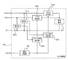
図1は、この発明の実施の形態1に係るワイヤ放電加工装置を示すブロック構成図である。
図1において、このワイヤ放電加工装置は、放電加工を行う放電加工部1と、放電加工部1の動作を制御する加工制御部2とを備えている。
1 is a block configuration diagram showing a wire electric discharge machining apparatus according to
In FIG. 1, the wire electric discharge machining apparatus includes an electric
まず、放電加工部1の構成について説明する。
2本のワイヤ11a、11bは、2個のワイヤボビン12a、12bからそれぞれ一定の速さで繰り出されている。ワイヤ11aは、2個のガイドローラ13a、13bに巻き掛けられている。また、ワイヤ11bは、2個のガイドローラ13c、13dに巻き掛けられている。
First, the configuration of the electric
The two
被加工物であるシリコンブロック3は、その一面(加工面)が、ワイヤ11aのガイドローラ13a、13bに挟まれた部分、およびワイヤ11bのガイドローラ13c、13dに挟まれた部分と対向するように配置されている。以下、ワイヤ11a、11bとシリコンブロック3とが対向した部分を、それぞれ対向部14a、14bと称する。
The
また、シリコンブロック3は、モータ15(駆動手段)に接続されたテーブル16(駆動手段)上に固定されている。テーブル16は、モータ15の駆動によって移動され、シリコンブロック3をワイヤ11a、11bに対して切断送りする。モータ15は、加工制御部2からの駆動制御信号によって駆動される。通常時には、シリコンブロック3は、一定の送り速度でワイヤ11a、11bに対して切断送りされている。
The
また、シリコンブロック3とワイヤ11a、11bの各々との間には、加工制御部2によりパルス電圧が印加される。ワイヤ11a、11bは、それぞれ対向部14a、14bにおいて放電を生じさせることにより、シリコンブロック3を放電加工する。なお、ワイヤ11a、11bには、ワイヤ11a、11bとそれぞれ接触する給電子17a、17bを介して電力が供給される。
Further, a pulse voltage is applied between the
続いて、加工制御部2の構成について説明する。
加工制御部2は、電圧計21a、21b(電圧検出手段)と、パルス波形設定部22(パルス波形設定手段)と、直流電源23(電源手段)と、パルス生成部24a、24b(パルス生成手段)と、駆動制御部25(駆動制御手段)とを含んでいる。
ここで、パルス波形設定部22、パルス生成部24a、24bおよび駆動制御部25は、CPUとプログラムを格納したメモリとを有するマイクロプロセッサ(図示せず)で構成されている。
Then, the structure of the
The
Here, the pulse
次に、加工制御部2の機能について説明する。
電圧計21aは、シリコンブロック3とワイヤ11aとの間の電圧を検出し、電圧検出値をパルス波形設定部22に出力する。また、電圧計21bは、シリコンブロック3とワイヤ11bとの間の電圧を検出し、電圧検出値をパルス波形設定部22に出力する。
Next, functions of the
The
パルス波形設定部22は、電圧計21a、21bからの電圧検出値に基づいて、パルス電圧信号(後述する)の信号波形を設定する。また、パルス波形設定部22は、設定した信号波形に対応したパルス波形信号をパルス生成部24a、24bの各々に出力する。なお、パルス波形設定部22の詳細な動作については後述する。
直流電源23は、パルス生成部24a、24bの各々に直流電力を供給する。
The pulse
The DC
パルス生成部24aは、パルス波形設定部22からのパルス波形信号と直流電源23からの直流電力とに基づいて、シリコンブロック3とワイヤ11aとの間にパルス電圧を印加するためのパルス電圧信号を生成する。また、パルス生成部24bは、パルス波形信号と直流電力とに基づいて、シリコンブロック3とワイヤ11bとの間にパルス電圧を印加するためのパルス電圧信号を生成する。また、パルス生成部24a、24bは、生成したパルス電圧信号をそれぞれワイヤ11a、11bに出力する。
The
駆動制御部25は、パルス波形設定部22に接続されている。また、駆動制御部25は、モータ15に対する駆動制御信号を出力して、モータ15の動作を制御する。なお、駆動制御部25の詳細な動作については後述する。
The
以下、図1とともに、図2のフローチャートを参照しながら、パルス波形設定部22の動作について説明する。パルス波形設定部22は、所定の周期で図2のフローチャートに示された動作を繰り返し実行する。
まず、パルス波形設定部22は、電圧計21a、21bでそれぞれ検出された電圧検出値を取り込む(ステップS31)。
The operation of the pulse
First, the pulse
このとき、電圧計21a、21bで検出される電圧は、一般的にパルス状に変化する。そこで、電圧計21a、21bは、パルスの1周期以上の平均値、ON状態の平均値、パルスがON状態になってから一定時間(例えば、1〜数十μsec)が経過した後からパルスがOFF状態になるまでの平均値、パルス1周期中の電圧の絶対値の最大値、所定時間(例えば数十μsecから数十msec)内の絶対値の最小値等を電圧検出値として出力する。また、電圧計21a、21bは、パルスの周期よりも十分に長い時定数を有するローパスフィルタのフィルタ処理後の値、上記検出値の中で少なくとも2つ以上を組み合わせた処理後の値(例えばパルス1周期中の電圧の絶対値の最大値の所定時間内の最小値)を電圧検出値として出力してもよい。
At this time, the voltages detected by the
続いて、パルス波形設定部22は、取り込んだ電圧検出値から、絶対値が最も低い電圧値Vminを選択する(ステップS32)。
次に、パルス波形設定部22は、電圧値Vminに基づいて、パルス波形テーブルから、パルス電圧信号の信号波形を設定する(ステップS33)。
Subsequently, the pulse
Next, the pulse
ここで、パルス波形テーブルは、電圧値とパルス電圧信号の信号波形との関係が記されたテーブルであり、パルス波形設定部22に記憶されている。
パルス波形テーブルの電圧値側は、被加工物の材質や電源電圧等に応じて設定される所定電圧値を境界として、通常電圧領域と電圧低下領域とに区分されている。電圧低下領域における信号波形は、通常電圧領域の信号波形と比較して、例えばパルスON時間が短く、かつパルスOFF時間が長くなっており、放電加工の加工エネルギが低下する波形になっている。
Here, the pulse waveform table is a table in which the relationship between the voltage value and the signal waveform of the pulse voltage signal is described, and is stored in the pulse
The voltage value side of the pulse waveform table is divided into a normal voltage region and a voltage drop region with a predetermined voltage value set according to the material of the workpiece, the power supply voltage, and the like as a boundary. The signal waveform in the voltage drop region has a waveform in which, for example, the pulse ON time is short and the pulse OFF time is long compared to the signal waveform in the normal voltage region, so that the machining energy of electric discharge machining is reduced.
なお、電圧低下領域における信号波形は、パルスON時間のみが短くなってもよいし、パルスOFF時間のみが長くなってもよい。また、この信号波形は、ピーク値が通常電圧領域の信号波形よりも低くなっていてもよいし、一定のパルス休止時間を含む波形であってもよい。
また、電圧低下領域は、電圧値に応じてさらに複数の領域に区分され、電圧値が小さくなるにつれてパルスON時間の割合が減少するような信号波形が設定されていてもよい。
In the signal waveform in the voltage drop region, only the pulse ON time may be shortened or only the pulse OFF time may be lengthened. Further, this signal waveform may have a peak value lower than the signal waveform in the normal voltage region, or may be a waveform including a certain pulse pause time.
The voltage drop region may be further divided into a plurality of regions according to the voltage value, and a signal waveform may be set such that the ratio of the pulse ON time decreases as the voltage value decreases.
続いて、パルス波形設定部22は、ステップS33で設定した信号波形に対応したパルス波形信号を、パルス生成部24a、24bの各々に出力し(ステップS34)、図2の処理を終了する。
Subsequently, the pulse
すなわち、放電加工の加工状態が良好な場合(通常時)には、パルス波形設定部22は、通常電圧領域の信号波形を設定する。
また、例えばワイヤ11aの振動、またはシリコンブロック3とワイヤ11aとの間に加工屑等が挟まることにより短時間の短絡が発生し、加工状態が一時的に悪化した場合に、パルス波形設定部22は、電圧低下領域の信号波形を設定する。これにより、シリコンブロック3とワイヤ11aとの間に高い短絡電流が流れることを防止して、ワイヤ11aの断線を防止することができる。
また、パルス波形設定部22は、加工状態が改善した後に通常電圧領域の信号波形を設定することで、放電加工の加工速度の低下を抑制することができる。
That is, when the machining state of the electric discharge machining is good (normal time), the pulse
In addition, for example, when a short-circuit occurs for a short time due to vibration of the
Further, the pulse
次に、駆動制御部25の動作について説明する。
駆動制御部25は、例えばワイヤ11aとシリコンブロック3とが通常時よりも接近し、電圧値Vminが所定電圧値よりも低い状態が第1所定時間以上継続した場合に、シリコンブロック3の切断送りの送り速度を低下させる駆動制御信号をモータ15に出力する。また、駆動制御部25は、電圧値Vminが所定電圧値よりも低い状態が、第1所定時間よりも長い第2所定時間以上継続した場合に、シリコンブロック3の切断送りを停止する駆動制御信号をモータ15に出力する。
これにより、パルス電圧信号の信号波形を変更しただけでは放電加工の加工状態が改善しない場合であっても、切断送りの送り速度を低下、または切断送りを停止することにより、放電加工の加工状態を改善することができる。
Next, the operation of the
For example, when the
As a result, even if the signal waveform of the pulse voltage signal is not changed, even if the machining state of electrical discharge machining is not improved, the machining state of electrical discharge machining can be reduced by reducing the cutting feed rate or stopping the cutting feed. Can be improved.
なお、駆動制御部25は、パルス波形設定部22から、電圧低下領域における信号波形に対応したパルス波形信号が出力されている状態を、電圧値Vminが所定電圧値よりも低い状態と判断している。
また、駆動制御部25は、電圧値Vminが所定電圧値よりも低い状態を検知した場合に、すぐに切断送りの送り速度を低下させる駆動制御信号を出力してもよい。
また、駆動制御部25は、電圧値Vminが所定電圧値よりも低い状態が第1所定時間以上継続した場合に、時間が長くなるにつれて切断送りの送り速度が低下するような駆動制御信号を出力してもよい。
The
Further, the
In addition, the
また、駆動制御部25は、電圧値Vminが所定電圧値よりも低い状態が第2所定時間以上継続した場合に、シリコンブロック3をワイヤ11a、11bから遠ざける駆動制御信号を出力してもよい。
また、駆動制御部25は、電圧値Vminが所定電圧値よりも高い場合に、これらの電圧値の差に応じて、切断送りの送り速度を通常時よりも速くする駆動制御信号を出力してもよい。
Further, the
In addition, when the voltage value Vmin is higher than the predetermined voltage value, the
この発明の実施の形態1に係るワイヤ放電加工装置によれば、制御可能な周波数帯域の低い機械的制御に代えて、高い周波数帯域で制御可能な電気的制御を主な制御として行うことにより、放電加工の加工制御を高速に行う。
具体的には、パルス波形設定部22は、電圧値Vminが所定電圧値よりも低い場合に、パルス電圧信号の信号波形として、電圧低下領域の信号波形を設定する。
そのため、放電加工の加工状態が一時的に悪化した場合であっても、適切なタイミングで放電加工の加工制御を行い、ワイヤの断線を防止することができる
また、パルス波形設定部22が電圧値Vminに基づいてパルス電圧信号の信号波形を設定することにより、最も加工状態が悪い箇所にあわせてパルス電圧信号の信号波形を設定することができる。
According to the wire electric discharge machining apparatus according to
Specifically, the pulse
Therefore, even if the machining state of the electric discharge machining is temporarily deteriorated, the machining of the electric discharge machining can be controlled at an appropriate timing to prevent the wire from being disconnected. Further, the pulse
また、パルス波形設定部22は、パルス生成部24a、24bに対して、同一のパルス波形信号を出力する。これにより、例えばパルス生成部24a、24bを一体的に構成して共通化することができる。この実施の形態では、ワイヤが2本の例を示したが、例えば100本のワイヤを備えた放電加工装置においては、パルス生成部を共通化することにより、放電加工装置を小型化するとともに、製造コストを大幅に削減することができる。
The pulse
なお、上記実施の形態1では、ワイヤ11a、11bを固定して、シリコンブロック3をワイヤ11a、11bに対して切断送りする場合を例に挙げて説明したが、これに限定されない。
シリコンブロック3を固定して、ワイヤ11a、11bに設けられる駆動手段により、ワイヤ11a、11bをシリコンブロック3に対して切断送りする場合でも、同様の効果を奏することができる。
In the first embodiment, the case where the
Even when the
また、上記実施の形態1では、2本の独立したワイヤ11a、11bが、対向部14a、14bでシリコンブロック3の加工面と対向しているものを例に挙げて説明した。
しかしながら、これに限定されず、1本のワイヤが1つの対向部でシリコンブロック3の加工面と対向する場合でも、同様の効果を奏することができる。
また、3本以上の独立したワイヤが、3箇所以上の対向部でシリコンブロック3と対向する場合や、1本のワイヤをガイドローラに複数回巻き掛けることにより、複数の対向部でシリコンブロック3と対向する場合でも、同様の効果を奏することができる。
In the first embodiment, the case where the two
However, the present invention is not limited to this, and the same effect can be achieved even when one wire faces the processed surface of the
In addition, when three or more independent wires face the
なお、3箇所以上の対向部でシリコンブロック3と対向する場合には、少なくとも2箇所の対向部に対応して電圧計が設けられ、これらの電圧計からの検出値のうち、絶対値が最も低い電圧値に基づいて、パルス電圧信号の信号波形が設定される。
このとき、電圧計が設けられる箇所は、任意に設定されてもよいし、シリコンブロック3の形状に応じて設定されてもよい。
In addition, when facing the
At this time, the location where the voltmeter is provided may be set arbitrarily, or may be set according to the shape of the
以下、図1、図2とともに、図3を参照しながら、シリコンブロック3の形状に応じて電圧計を設ける箇所を設定する方法について説明する。
図3において、ワイヤ11a〜11fは、それぞれ対向部14a〜14fでシリコンブロック3の加工面と対向している。
ここで、シリコンブロック3の加工面と、ワイヤ11a〜11fのなす面とは、平行ではなく傾いている。一般的に、シリコンブロック3をテーブル16に固定する際に、加工面をワイヤ11a〜11fのなす面と完全に平行に固定することは困難であり、多少の傾きが生じる。このとき、ワイヤ11a〜11fのうち、シリコンブロック3に最も接近し、電圧値が低くなっているのは、ワイヤ11aまたはワイヤ11fの何れかになる。
Hereinafter, a method of setting a location where a voltmeter is provided according to the shape of the
In FIG. 3, the
Here, the processed surface of the
そこで、対向部14aおよび対向部14fに対応して電圧計を設ける。
パルス波形設定部22は、対向部14a、14fに対応して設けられた電圧計からの検出値のうち、絶対値が低い方の電圧値に基づいて、パルス電圧信号の信号波形を設定する。
そのため、加工状態が悪い箇所にあわせてパルス電圧信号の信号波形を設定することができる。また、シリコンブロック3と対向するワイヤの本数と比較して、少ない電圧計で加工制御部2を構成することができるので、放電加工装置を小型化するとともに、製造コストを大幅に削減することができる。
なお、電圧計を設ける箇所を設定する他の方法としては、所定本数のワイヤ毎に電圧計を設ける方法が考えられる。また、シリコンブロック3の加工面の幅がワイヤの幅より狭い場合に、加工面の両端に対応するワイヤに電圧計を設ける方法等が考えられる。
Therefore, a voltmeter is provided corresponding to the facing
The pulse
Therefore, it is possible to set the signal waveform of the pulse voltage signal in accordance with the location where the machining state is bad. Moreover, since the
In addition, as another method of setting a location where a voltmeter is provided, a method of providing a voltmeter for each predetermined number of wires is conceivable. In addition, when the width of the processed surface of the
実施の形態2.
上記実施の形態1では、パルス波形設定部22は、電圧検出値のうち、絶対値が最も低い電圧値に基づいて、パルス電圧信号の信号波形を設定するとした。
しかしながら、これに限定されず、パルス波形設定部22は、電圧検出値の絶対値の平均値に基づいて、パルス電圧信号の信号波形を設定してもよい。
In the first embodiment, the pulse
However, the present invention is not limited to this, and the pulse
以下、図1とともに、図4のフローチャートを参照しながら、パルス波形設定部22が、電圧検出値の絶対値の平均値に基づいてパルス電圧信号の信号波形を設定する処理について説明する。
なお、実施の形態2に係るワイヤ放電加工装置の構成は、前述の実施の形態1と同様であり、その説明を省略する。
Hereinafter, a process in which the pulse
Note that the configuration of the wire electric discharge machining apparatus according to the second embodiment is the same as that of the first embodiment, and a description thereof will be omitted.
まず、パルス波形設定部22は、電圧計21a、21bでそれぞれ検出された電圧検出値を取り込む(ステップS41)。
続いて、パルス波形設定部22は、取り込んだ電圧検出値の絶対値の平均値Vmeanを算出する(ステップS42)。
First, the pulse
Subsequently, the pulse
次に、パルス波形設定部22は、平均値Vmeanに基づいて、パルス波形テーブルから、パルス電圧信号の信号波形を設定する(ステップS43)。
続いて、パルス波形設定部22は、ステップS43で設定した信号波形に対応したパルス波形信号を、パルス生成部24a、24bの各々に出力し(ステップS44)、図4の処理を終了する。
Next, the pulse
Subsequently, the pulse
このとき、駆動制御部25は、平均値Vmeanが所定電圧値よりも低い状態が、第1所定時間以上または第2所定時間以上継続した場合に、シリコンブロック3の切断送りの送り速度を低下させるか、または切断送りを停止する。
その他の動作については、前述の実施の形態1と同様であり、その説明を省略する。
At this time, the
Other operations are the same as those in the first embodiment, and a description thereof is omitted.
この発明の実施の形態2に係るワイヤ放電加工装置によれば、パルス波形設定部22は、平均値Vmeanが所定電圧値よりも低い場合に、パルス電圧信号の信号波形として、電圧低下領域の信号波形を設定する。
そのため、ノイズ等による検出誤差の影響を抑制することができ、良好な加工状態を維持することができる。
According to the wire electric discharge machining apparatus according to
Therefore, the influence of detection error due to noise or the like can be suppressed, and a good machining state can be maintained.
また、前述した実施の形態1と同様に、パルス波形設定部22は、パルス生成部24a、24bに対して、同一のパルス波形信号を出力する。そのため、多数のワイヤを備えた放電加工装置においては、パルス生成部を共通化することにより、放電加工装置を小型化するとともに、製造コストを大幅に削減することができる。
As in the first embodiment, the pulse
実施の形態3.
図5は、この発明の実施の形態3に係るワイヤ放電加工装置の加工制御部2Aを示すブロック構成図である。
図5において、加工制御部2Aは、図1に示したパルス波形設定部22に代えて、パルス波形設定部22a、22b(パルス波形設定手段)を備えている。
その他の構成については、前述の実施の形態1と同様であり、その説明を省略する。
FIG. 5 is a block configuration diagram showing a
In FIG. 5, the
Other configurations are the same as those of the first embodiment, and the description thereof is omitted.
次に、加工制御部2Aの機能について説明する。
電圧計21aは、シリコンブロック3とワイヤ11aとの間の電圧を検出し、電圧検出値をパルス波形設定部22aに出力する。また、電圧計21bは、シリコンブロック3とワイヤ11bとの間の電圧を検出し、電圧検出値をパルス波形設定部22bに出力する。
Next, functions of the
The
パルス波形設定部22aは、電圧計21aからの電圧検出値に基づいて、ワイヤ11aに対するパルス電圧信号の信号波形を設定して出力する。パルス波形設定部22bは、電圧計21bからの電圧検出値に基づいて、ワイヤ11bに対するパルス電圧信号の信号波形を設定して出力する。
The pulse
パルス生成部24aは、パルス波形設定部22aからのパルス波形信号と直流電源23からの直流電力とに基づいて、シリコンブロック3とワイヤ11aとの間にパルス電圧を印加するためのパルス電圧信号を生成する。また、パルス生成部24bは、パルス波形設定部22bからのパルス波形信号と直流電力とに基づいて、シリコンブロック3とワイヤ11bとの間にパルス電圧を印加するためのパルス電圧信号を生成する。
その他の動作については、前述の実施の形態1と同様であり、その説明を省略する。
The
Other operations are the same as those in the first embodiment, and a description thereof is omitted.
この発明の実施の形態3に係るワイヤ放電加工装置によれば、パルス波形設定部22a、22bは、それぞれワイヤ11a、11bの加工状態に対応したパルス電圧信号の信号波形を設定する。すなわち、パルス波形設定部22a、22bは、加工状態が良好なワイヤにおけるパルス電圧信号を変更することなく、加工状態が悪化したワイヤについてのみパルス電圧信号を変更する。
そのため、加工状態が良好な箇所における加工状態を維持しつつ、ワイヤの断線を防止することができるとともに、放電加工の加工速度の低下を抑制することができる。
According to the wire electric discharge machining apparatus according to
For this reason, it is possible to prevent the wire from being disconnected while maintaining the machining state in a portion where the machining state is good, and to suppress a reduction in the machining speed of the electric discharge machining.
なお、上記実施の形態3では、ワイヤが2本である場合について、2本のワイヤそれぞれに電圧計、パルス生成部およびパルス波形設定部を設けた場合について説明したが、これに限定されない。例えば図3のようにワイヤを6本有する場合であって、その両端(1本目および6本目)のワイヤにそれぞれ電圧計、パルス生成部およびパルス波形設定部が設けられていてもよい。
このとき、2本目および3本目のワイヤには、1本目のワイヤに設けられたパルス波形設定部で設定された信号波形に基づいてパルス電圧が印加される。また、4本目および5本目のワイヤには、6本目のワイヤに設けられたパルス波形設定部で設定された信号波形に基づいてパルス電圧が印加される。
In
At this time, a pulse voltage is applied to the second and third wires based on the signal waveform set by the pulse waveform setting unit provided on the first wire. A pulse voltage is applied to the fourth and fifth wires based on the signal waveform set by the pulse waveform setting unit provided on the sixth wire.
1 放電加工部、2、2A 加工制御部、3 シリコンブロック(被加工物)、11a〜11f ワイヤ、14a〜14f 対向部、15 モータ(駆動手段)、16 テーブル(駆動手段)、21a、21b 電圧計(電圧検出手段)、22、22a、22b パルス波形設定部(パルス波形設定手段)、23 直流電源(電源手段)、24a、24b パルス生成部(パルス生成手段)、25 駆動制御部(駆動制御手段)。
DESCRIPTION OF
Claims (8)
前記被加工物と前記ワイヤとの間にパルス電圧を印加するためのパルス電圧信号を生成するパルス生成手段と、
前記パルス生成手段に直流電力を供給する電源手段と、
前記被加工物と前記ワイヤとの間の電圧を検出する電圧検出手段と、
前記電圧検出手段で検出された電圧検出値に基づいて前記パルス電圧信号の信号波形を設定し、前記信号波形に対応したパルス波形信号を前記パルス生成手段に出力するパルス波形設定手段と、を備え、
前記パルス波形設定手段は、前記電圧検出値の絶対値が所定電圧値よりも低い場合に、前記放電加工の加工エネルギが低下するように前記信号波形を設定することを特徴とするワイヤ放電加工装置。 A wire for electric discharge machining the workpiece by causing an electric discharge at a facing portion facing the workpiece;
Pulse generation means for generating a pulse voltage signal for applying a pulse voltage between the workpiece and the wire;
Power supply means for supplying DC power to the pulse generating means;
Voltage detection means for detecting a voltage between the workpiece and the wire;
Pulse waveform setting means for setting a signal waveform of the pulse voltage signal based on a voltage detection value detected by the voltage detection means and outputting a pulse waveform signal corresponding to the signal waveform to the pulse generation means. ,
The pulse waveform setting means sets the signal waveform so that the machining energy of the electrical discharge machining is reduced when the absolute value of the voltage detection value is lower than a predetermined voltage value. .
前記駆動手段の動作を制御する駆動制御手段と、を備え、
前記駆動制御手段は、前記電圧検出値の絶対値が前記所定電圧値よりも低い状態が第1所定時間以上継続した場合に、前記切断送りの送り速度を低下させることを特徴とする請求項1に記載のワイヤ放電加工装置。 Driving means for supporting the workpiece and cutting and feeding the workpiece to the wire;
Drive control means for controlling the operation of the drive means,
The drive control means reduces the feed speed of the cutting feed when a state where the absolute value of the voltage detection value is lower than the predetermined voltage value continues for a first predetermined time or longer. The wire electric discharge machining apparatus according to 1.
前記駆動手段の動作を制御する駆動制御手段と、を備え、
前記駆動制御手段は、前記電圧検出値の絶対値が前記所定電圧値よりも低い状態が第1所定時間以上継続した場合に、前記切断送りの送り速度を低下させることを特徴とする請求項1に記載のワイヤ放電加工装置。 Drive means provided on the wire and cutting and feeding the wire to the workpiece;
Drive control means for controlling the operation of the drive means,
The drive control means reduces the feed speed of the cutting feed when a state where the absolute value of the voltage detection value is lower than the predetermined voltage value continues for a first predetermined time or longer. The wire electric discharge machining apparatus according to 1.
前記複数の対向部の少なくとも2箇所に対応して前記電圧検出手段を備え、
前記パルス波形設定手段は、前記電圧検出手段で検出された複数の電圧検出値のうち、絶対値が最も低い電圧値に基づいて、前記信号波形を設定することを特徴とする請求項1から請求項4までの何れか1項に記載のワイヤ放電加工装置。 The workpiece and the wire face each other at the plurality of facing portions,
The voltage detection means corresponding to at least two of the plurality of facing portions;
The pulse waveform setting unit sets the signal waveform based on a voltage value having the lowest absolute value among a plurality of voltage detection values detected by the voltage detection unit. Item 5. The wire electric discharge machining apparatus according to any one of Items 1 to 4.
前記複数の対向部の少なくとも2箇所に対応して前記電圧検出手段を備え、
前記パルス波形設定手段は、前記電圧検出手段で検出された複数の電圧検出値の絶対値の平均値に基づいて、前記信号波形を設定することを特徴とする請求項1から請求項4までの何れか1項に記載のワイヤ放電加工装置。 The workpiece and the wire face each other at the plurality of facing portions,
The voltage detection means corresponding to at least two of the plurality of facing portions;
5. The pulse waveform setting unit sets the signal waveform based on an average value of absolute values of a plurality of voltage detection values detected by the voltage detection unit. The wire electric discharge machining apparatus according to any one of the above.
前記複数の対向部の少なくとも2箇所に対応して前記電圧検出手段、前記パルス生成手段および前記パルス波形設定手段をそれぞれ備えたことを特徴とする請求項1から請求項4までの何れか1項に記載のワイヤ放電加工装置。 The workpiece and the wire face each other at the plurality of facing portions,
The voltage detection means, the pulse generation means, and the pulse waveform setting means are provided corresponding to at least two locations of the plurality of facing portions, respectively. The wire electric discharge machining apparatus according to 1.
Priority Applications (1)
| Application Number | Priority Date | Filing Date | Title |
|---|---|---|---|
| JP2008071828A JP2009226504A (en) | 2008-03-19 | 2008-03-19 | Wire electric discharge machining device |
Applications Claiming Priority (1)
| Application Number | Priority Date | Filing Date | Title |
|---|---|---|---|
| JP2008071828A JP2009226504A (en) | 2008-03-19 | 2008-03-19 | Wire electric discharge machining device |
Publications (1)
| Publication Number | Publication Date |
|---|---|
| JP2009226504A true JP2009226504A (en) | 2009-10-08 |
Family
ID=41242535
Family Applications (1)
| Application Number | Title | Priority Date | Filing Date |
|---|---|---|---|
| JP2008071828A Pending JP2009226504A (en) | 2008-03-19 | 2008-03-19 | Wire electric discharge machining device |
Country Status (1)
| Country | Link |
|---|---|
| JP (1) | JP2009226504A (en) |
Cited By (8)
| Publication number | Priority date | Publication date | Assignee | Title |
|---|---|---|---|---|
| US20120312787A1 (en) * | 2010-04-09 | 2012-12-13 | Mitsubishi Electric Corporation | Electrical discharge machining apparatus and electrical discharge machining method |
| US20130180866A1 (en) * | 2011-12-30 | 2013-07-18 | Agie Charmilles Sa | Wire cutting method |
| WO2013108530A1 (en) * | 2012-01-18 | 2013-07-25 | 三菱電機株式会社 | Wire discharge machining device, wire discharge machining method, thin-plate manufacturing method, and semiconductor wafer manufacturing method |
| JP2013144330A (en) * | 2012-01-13 | 2013-07-25 | Mitsubishi Electric Corp | Multiwire electric discharge machining device and multiwire electric discharge machining method |
| JP2013144329A (en) * | 2012-01-13 | 2013-07-25 | Mitsubishi Electric Corp | Multiwire electric discharge machining apparatus and multiwire electric discharge machining method |
| JP2014008592A (en) * | 2012-07-02 | 2014-01-20 | Mitsubishi Electric Corp | Multiwire electric discharge machining device, multiwire electric discharge machining method, thin plate manufacturing method, and semiconductor wafer manufacturing method |
| RU2562558C2 (en) * | 2012-10-01 | 2015-09-10 | Общество с ограниченной ответственностью "ЕДМ инжиниринг" | Wire edm machine |
| JP2016163920A (en) * | 2015-03-06 | 2016-09-08 | 株式会社ディスコ | Multi-wire electrical discharge machining apparatus |
Citations (5)
| Publication number | Priority date | Publication date | Assignee | Title |
|---|---|---|---|---|
| JPS55137837A (en) * | 1979-04-03 | 1980-10-28 | Mitsubishi Electric Corp | Wire cut type electric discharge machining |
| JPS5866626A (en) * | 1981-10-12 | 1983-04-20 | Hitachi Ltd | Feed controller of electric discharge machining |
| WO1993001017A1 (en) * | 1991-07-05 | 1993-01-21 | Sodick Co., Ltd. | Wirecut electric discharge machining system |
| JP2000107941A (en) * | 1998-10-01 | 2000-04-18 | Toyo Advanced Technologies Co Ltd | Electric discharge machining method and discharge type wire saw |
| JP2007168056A (en) * | 2005-12-26 | 2007-07-05 | Fanuc Ltd | Wire cut electric discharge processing machine |
-
2008
- 2008-03-19 JP JP2008071828A patent/JP2009226504A/en active Pending
Patent Citations (5)
| Publication number | Priority date | Publication date | Assignee | Title |
|---|---|---|---|---|
| JPS55137837A (en) * | 1979-04-03 | 1980-10-28 | Mitsubishi Electric Corp | Wire cut type electric discharge machining |
| JPS5866626A (en) * | 1981-10-12 | 1983-04-20 | Hitachi Ltd | Feed controller of electric discharge machining |
| WO1993001017A1 (en) * | 1991-07-05 | 1993-01-21 | Sodick Co., Ltd. | Wirecut electric discharge machining system |
| JP2000107941A (en) * | 1998-10-01 | 2000-04-18 | Toyo Advanced Technologies Co Ltd | Electric discharge machining method and discharge type wire saw |
| JP2007168056A (en) * | 2005-12-26 | 2007-07-05 | Fanuc Ltd | Wire cut electric discharge processing machine |
Cited By (12)
| Publication number | Priority date | Publication date | Assignee | Title |
|---|---|---|---|---|
| US20120312787A1 (en) * | 2010-04-09 | 2012-12-13 | Mitsubishi Electric Corporation | Electrical discharge machining apparatus and electrical discharge machining method |
| US20130180866A1 (en) * | 2011-12-30 | 2013-07-18 | Agie Charmilles Sa | Wire cutting method |
| US9193020B2 (en) * | 2011-12-30 | 2015-11-24 | Agie Charmilles Sa | Wire cutting method |
| JP2013144330A (en) * | 2012-01-13 | 2013-07-25 | Mitsubishi Electric Corp | Multiwire electric discharge machining device and multiwire electric discharge machining method |
| JP2013144329A (en) * | 2012-01-13 | 2013-07-25 | Mitsubishi Electric Corp | Multiwire electric discharge machining apparatus and multiwire electric discharge machining method |
| WO2013108530A1 (en) * | 2012-01-18 | 2013-07-25 | 三菱電機株式会社 | Wire discharge machining device, wire discharge machining method, thin-plate manufacturing method, and semiconductor wafer manufacturing method |
| CN104053520A (en) * | 2012-01-18 | 2014-09-17 | 三菱电机株式会社 | Wire Discharge Machining Device, Wire Discharge Machining Method, Thin-plate Manufacturing Method, And Semiconductor Wafer Manufacturing Method |
| JPWO2013108530A1 (en) * | 2012-01-18 | 2015-05-11 | 三菱電機株式会社 | Wire electrical discharge machine |
| US9707638B2 (en) | 2012-01-18 | 2017-07-18 | Mitsubishi Electric Corporation | Wire electric-discharge machining device, wire electric-discharge machining method, thin-plate manufacturing method, and semiconductor wafer manufacturing method |
| JP2014008592A (en) * | 2012-07-02 | 2014-01-20 | Mitsubishi Electric Corp | Multiwire electric discharge machining device, multiwire electric discharge machining method, thin plate manufacturing method, and semiconductor wafer manufacturing method |
| RU2562558C2 (en) * | 2012-10-01 | 2015-09-10 | Общество с ограниченной ответственностью "ЕДМ инжиниринг" | Wire edm machine |
| JP2016163920A (en) * | 2015-03-06 | 2016-09-08 | 株式会社ディスコ | Multi-wire electrical discharge machining apparatus |
Similar Documents
| Publication | Publication Date | Title |
|---|---|---|
| JP2009226504A (en) | Wire electric discharge machining device | |
| JPWO2007032114A1 (en) | Wire electric discharge machining apparatus and wire electric discharge machining method | |
| JP2010260151A (en) | Wire electric discharge machining device and method for electric discharge machining | |
| KR102193083B1 (en) | Arc welding control method | |
| JP2011016172A (en) | Wire-cut electric discharge machine having function to suppress local production of streaks during finish machining | |
| WO2011002108A1 (en) | Wire electric-discharge-machining apparatus | |
| WO2011125656A1 (en) | Electrical discharge machining apparatus and electrical discharge machining method | |
| KR102206137B1 (en) | Wire electrical discharge machine | |
| EP2985105B1 (en) | Wire electric discharge machine determining whether or not electrical discharge machining of workpiece can be perfomed | |
| JP5005116B1 (en) | Wire electrical discharge machine | |
| JP4603605B2 (en) | Wire electrical discharge machine with electrode pin detachment / push detection function | |
| US20140014624A1 (en) | Wire electric discharge machine with machining power source switchable for wire cutting | |
| US10493547B2 (en) | Wire electrical discharge machining device | |
| JP2013035080A (en) | Wire saw | |
| US10189102B2 (en) | Electric discharge machine | |
| KR102106651B1 (en) | Power supply device for arc-welding and control method of power supply device for arc-welding | |
| JP5044898B2 (en) | Power supply device for electric discharge machine and wire electric discharge machine | |
| CN109332830A (en) | The wire drive device and method of to-and-fro wire-travelling type electric spark linear cutting machine | |
| JP5236368B2 (en) | Wire electrical discharge machine with single power supply | |
| KR101235485B1 (en) | AC Electric Power for Wire Cut Discharging Manufacturing Unit | |
| JP2801280B2 (en) | Wire cut EDM power supply | |
| WO2002034443A1 (en) | Wire electric discharge machine | |
| JP2014172096A (en) | Wire electrical discharge machining system, power supply device, and control method and program thereof | |
| JP2008062303A (en) | Control method for wire electric discharge machine | |
| JP2009136051A (en) | Compressor controller |
Legal Events
| Date | Code | Title | Description |
|---|---|---|---|
| A621 | Written request for application examination |
Free format text: JAPANESE INTERMEDIATE CODE: A621 Effective date: 20100107 |
|
| A977 | Report on retrieval |
Free format text: JAPANESE INTERMEDIATE CODE: A971007 Effective date: 20101109 |
|
| A131 | Notification of reasons for refusal |
Effective date: 20120321 Free format text: JAPANESE INTERMEDIATE CODE: A131 |
|
| A02 | Decision of refusal |
Effective date: 20120710 Free format text: JAPANESE INTERMEDIATE CODE: A02 |