JP2009211202A - Memory system - Google Patents
Memory system Download PDFInfo
- Publication number
- JP2009211202A JP2009211202A JP2008051378A JP2008051378A JP2009211202A JP 2009211202 A JP2009211202 A JP 2009211202A JP 2008051378 A JP2008051378 A JP 2008051378A JP 2008051378 A JP2008051378 A JP 2008051378A JP 2009211202 A JP2009211202 A JP 2009211202A
- Authority
- JP
- Japan
- Prior art keywords
- management information
- storage
- pointer
- stored
- block
- Prior art date
- Legal status (The legal status is an assumption and is not a legal conclusion. Google has not performed a legal analysis and makes no representation as to the accuracy of the status listed.)
- Abandoned
Links
Images


Classifications
-
- G—PHYSICS
- G06—COMPUTING; CALCULATING OR COUNTING
- G06F—ELECTRIC DIGITAL DATA PROCESSING
- G06F12/00—Accessing, addressing or allocating within memory systems or architectures
- G06F12/02—Addressing or allocation; Relocation
- G06F12/0223—User address space allocation, e.g. contiguous or non contiguous base addressing
- G06F12/023—Free address space management
- G06F12/0238—Memory management in non-volatile memory, e.g. resistive RAM or ferroelectric memory
- G06F12/0246—Memory management in non-volatile memory, e.g. resistive RAM or ferroelectric memory in block erasable memory, e.g. flash memory
-
- G—PHYSICS
- G11—INFORMATION STORAGE
- G11C—STATIC STORES
- G11C11/00—Digital stores characterised by the use of particular electric or magnetic storage elements; Storage elements therefor
- G11C11/56—Digital stores characterised by the use of particular electric or magnetic storage elements; Storage elements therefor using storage elements with more than two stable states represented by steps, e.g. of voltage, current, phase, frequency
- G11C11/5621—Digital stores characterised by the use of particular electric or magnetic storage elements; Storage elements therefor using storage elements with more than two stable states represented by steps, e.g. of voltage, current, phase, frequency using charge storage in a floating gate
- G11C11/5628—Programming or writing circuits; Data input circuits
-
- G—PHYSICS
- G11—INFORMATION STORAGE
- G11C—STATIC STORES
- G11C16/00—Erasable programmable read-only memories
- G11C16/02—Erasable programmable read-only memories electrically programmable
- G11C16/04—Erasable programmable read-only memories electrically programmable using variable threshold transistors, e.g. FAMOS
- G11C16/0483—Erasable programmable read-only memories electrically programmable using variable threshold transistors, e.g. FAMOS comprising cells having several storage transistors connected in series
-
- G—PHYSICS
- G11—INFORMATION STORAGE
- G11C—STATIC STORES
- G11C16/00—Erasable programmable read-only memories
- G11C16/02—Erasable programmable read-only memories electrically programmable
- G11C16/06—Auxiliary circuits, e.g. for writing into memory
- G11C16/10—Programming or data input circuits
- G11C16/102—External programming circuits, e.g. EPROM programmers; In-circuit programming or reprogramming; EPROM emulators
- G11C16/105—Circuits or methods for updating contents of nonvolatile memory, especially with 'security' features to ensure reliable replacement, i.e. preventing that old data is lost before new data is reliably written
-
- G—PHYSICS
- G11—INFORMATION STORAGE
- G11C—STATIC STORES
- G11C7/00—Arrangements for writing information into, or reading information out from, a digital store
- G11C7/20—Memory cell initialisation circuits, e.g. when powering up or down, memory clear, latent image memory
-
- G—PHYSICS
- G06—COMPUTING; CALCULATING OR COUNTING
- G06F—ELECTRIC DIGITAL DATA PROCESSING
- G06F11/00—Error detection; Error correction; Monitoring
- G06F11/07—Responding to the occurrence of a fault, e.g. fault tolerance
- G06F11/14—Error detection or correction of the data by redundancy in operation
- G06F11/1402—Saving, restoring, recovering or retrying
- G06F11/1471—Saving, restoring, recovering or retrying involving logging of persistent data for recovery
-
- G—PHYSICS
- G06—COMPUTING; CALCULATING OR COUNTING
- G06F—ELECTRIC DIGITAL DATA PROCESSING
- G06F2212/00—Indexing scheme relating to accessing, addressing or allocation within memory systems or architectures
- G06F2212/72—Details relating to flash memory management
- G06F2212/7207—Details relating to flash memory management management of metadata or control data
Landscapes
- Engineering & Computer Science (AREA)
- Microelectronics & Electronic Packaging (AREA)
- Theoretical Computer Science (AREA)
- Computer Hardware Design (AREA)
- Physics & Mathematics (AREA)
- General Engineering & Computer Science (AREA)
- General Physics & Mathematics (AREA)
- Computer Security & Cryptography (AREA)
- Techniques For Improving Reliability Of Storages (AREA)
Abstract
Description
本発明は、不揮発性半導体記憶装置を用いて構成されるメモリシステムに関する。 The present invention relates to a memory system configured using a nonvolatile semiconductor memory device.
ハードディスク装置を2次記憶装置として用いたパーソナルコンピュータにおいては、ハードディスク装置に格納されるデータが何らかの障害によって無効なデータとなってしまうことを防ぐためにバックアップをとる技術が知られている。たとえば、ハードディスク装置中のデータの変更を検出すると、そのデータの変更前のバックアップコピーであるスナップショットをとり、そのデータに対する更新を記録したログをとる。その後、所定の時間ごとにスナップショットをとるとともに、スナップショットをとる前の過去のログを無効にし、新しいログを生成するという処理が繰り返し行われる(たとえば、特許文献1参照)。そして、データが無効になってしまった場合には、スナップショットとログを基にそのデータを復元するようにしている。 In a personal computer using a hard disk device as a secondary storage device, a technique for taking a backup in order to prevent data stored in the hard disk device from becoming invalid data due to some trouble is known. For example, when a change in data in the hard disk device is detected, a snapshot which is a backup copy before the change of the data is taken, and a log in which updates to the data are recorded is taken. Thereafter, a process of taking a snapshot every predetermined time, invalidating a past log before taking the snapshot, and generating a new log is repeatedly performed (for example, see Patent Document 1). When the data becomes invalid, the data is restored based on the snapshot and the log.
ところで、近年では、不揮発性半導体記憶装置であるNAND型フラッシュメモリの大容量化が進行し、このNAND型フラッシュメモリを有するメモリシステムを2次記憶装置とするパーソナルコンピュータが製品化されている。しかし、このようなNAND型フラッシュメモリを2次記憶装置とするパーソナルコンピュータに格納されるデータのバックアップに対して、ハードディスク装置を2次記憶装置として想定した上記特許文献1の技術を適用することはできない。それは、NAND型フラッシュメモリの大容量化には、1つのメモリセルに2ビット以上の複数のデータ(多値データ)を記憶することが可能な多値メモリ技術が使用されているからである(たとえば、特許文献2参照)。 In recent years, the capacity of NAND flash memories, which are nonvolatile semiconductor memory devices, has been increased, and personal computers using a memory system having the NAND flash memory as a secondary storage device have been commercialized. However, it is not possible to apply the technique of the above-mentioned Patent Document 1 assuming that a hard disk device is a secondary storage device for backup of data stored in a personal computer having such a NAND flash memory as a secondary storage device. Can not. This is because a multi-level memory technology capable of storing a plurality of data (multi-level data) of 2 bits or more in one memory cell is used to increase the capacity of the NAND flash memory ( For example, see Patent Document 2).
多値メモリを構成するメモリセルは、チャネル領域上にゲート絶縁膜、浮遊ゲート電極、ゲート間絶縁膜および制御ゲート電極が順に積層された積層ゲート構造を有する電界効果型トランジスタ構造を有し、浮遊ゲート電極に蓄積される電子の数に応じて、複数の閾値電圧を設定可能な構成を有している。そして、この複数の閾値電圧によって多値記憶を可能とするために、1つのデータに対応する閾値電圧の分布を非常に狭く制御する必要がある。このような多値を記憶可能なメモリセルの書換可能回数には制約がある。 A memory cell constituting a multi-value memory has a field effect transistor structure having a stacked gate structure in which a gate insulating film, a floating gate electrode, an inter-gate insulating film, and a control gate electrode are sequentially stacked on a channel region. A plurality of threshold voltages can be set according to the number of electrons accumulated in the gate electrode. In order to enable multilevel storage using the plurality of threshold voltages, it is necessary to control the threshold voltage distribution corresponding to one data very narrowly. There is a limit to the number of times the memory cell capable of storing such multi-values can be rewritten.
特許文献1に記載のスナップショットとログを保存する方法では、そのスナップショットとログの保存場所にアクセスするためのポインタが必要であり、このポインタは、スナップショットとログの更新のたびに書換えられる。この書換えは、書換可能回数が無制限のハードディスク装置の場合には問題とならないが、上記したように書換可能回数に制限のある多値メモリを用いたNAND型フラッシュメモリの場合には、NAND型フラッシュメモリの寿命を短くしてしまうという問題点があった。 In the method of saving a snapshot and a log described in Patent Document 1, a pointer for accessing the storage location of the snapshot and the log is required, and this pointer is rewritten every time the snapshot and the log are updated. . This rewriting does not cause a problem in the case of a hard disk device with an unlimited number of rewritable times, but in the case of a NAND flash memory using a multi-level memory with a limited number of rewritable times as described above, There was a problem of shortening the memory life.
本発明は、多値メモリを使用したNAND型フラッシュメモリを有するメモリシステムで、スナップショットとログの保存場所にアクセスするためのポインタの書換えによるNAND型フラッシュメモリの低寿命化を抑制することができるメモリシステムを提供することを目的とする。 INDUSTRIAL APPLICABILITY The present invention is a memory system having a NAND flash memory using a multi-level memory, and can reduce the lifetime of the NAND flash memory due to rewriting of a pointer for accessing a snapshot and log storage location. An object is to provide a memory system.
本発明の一態様によれば、揮発性の第1の記憶部と、不揮発性の第2の記憶部と、前記第1の記憶部を介してホスト装置と前記第2の記憶部との間のデータ転送を行うとともに、起動時に前記第2の記憶部に記憶された前記データの格納位置を含む管理情報を前記第1の記憶部に取込み、該取り込んだ管理情報を更新しながら管理情報に基づいて前記第1および第2の記憶部でのデータ管理を行うコントローラと、を備え、前記第2の記憶部は、前記第1の記憶部に取り込まれた最新の状態の管理情報、および該最新の状態の管理情報の保存位置を示す保存位置情報を含む管理情報保存情報を保存する管理情報保存領域を有し、前記保存位置情報は、当該メモリシステムの起動時に前記コントローラによって読み込まれ、前記管理情報保存領域内の前記最新の状態の管理情報の格納位置を示す第2のポインタと、この第2のポインタの格納位置を示す第1のポインタとを含み、前記第1のポインタは前記第2の記憶部中の固定領域に格納され、前記第2のポインタは前記第2の記憶部中の前記固定領域を除いた領域に格納されることを特徴とするメモリシステムが提供される。 According to one aspect of the present invention, a volatile first storage unit, a nonvolatile second storage unit, and a host device and the second storage unit through the first storage unit. The management information including the storage location of the data stored in the second storage unit at the time of start-up is taken into the first storage unit, and the management information is updated while updating the fetched management information. And a controller that performs data management in the first and second storage units based on the management information of the latest state captured in the first storage unit, and the second storage unit, A management information storage area for storing management information storage information including storage location information indicating a storage location of the management information in the latest state; the storage location information is read by the controller when the memory system is activated; Management information storage A second pointer indicating the storage position of the management information in the latest state, and a first pointer indicating the storage position of the second pointer, wherein the first pointer is the second storage unit. The memory system is provided, wherein the second pointer is stored in an area excluding the fixed area in the second storage unit.
本発明によれば、多値メモリを使用したNAND型フラッシュメモリを有するメモリシステムで、スナップショットとログの保存場所にアクセスするためのポインタの書換えによるNAND型フラッシュメモリの低寿命化を抑制することができるという効果を奏する。 According to the present invention, in a memory system having a NAND flash memory using a multi-level memory, it is possible to suppress a reduction in the lifetime of the NAND flash memory due to rewriting of a pointer for accessing a snapshot and log storage location. There is an effect that can be.
以下に添付図面を参照して、本発明にかかるメモリシステムの最良な実施の形態を詳細に説明する。なお、これらの実施の形態により本発明が限定されるものではない。 Exemplary embodiments of a memory system according to the present invention will be explained below in detail with reference to the accompanying drawings. Note that the present invention is not limited to these embodiments.
(第1の実施の形態)
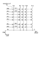
このメモリシステムは、不揮発性半導体記憶装置を含み、たとえば、パーソナルコンピュータなどのホスト装置の2次記憶装置(SSD:Solid State Drive)として使用され、ホスト装置から書込要求が出されたデータを記憶し、またホスト装置から読出要求のあったデータを読出してホスト装置に出力する機能を有する。図1は、本発明の第1の実施の形態にかかるメモリシステムの構成の一例を示すブロック図である。このメモリシステム10は、第1の記憶部としてのDRAM(Dynamic Random Access Memory)11と、第2の記憶部としてのNAND型フラッシュメモリ(以下、NANDメモリという)12と、電源回路13と、コントローラとしてのドライブ制御部14と、を備える。
(First embodiment)
This memory system includes a non-volatile semiconductor storage device and is used as a secondary storage device (SSD: Solid State Drive) of a host device such as a personal computer, for example, and stores data for which a write request is issued from the host device In addition, it has a function of reading data requested to be read from the host device and outputting it to the host device. FIG. 1 is a block diagram showing an example of the configuration of the memory system according to the first embodiment of the present invention. The
DRAM11は、データ転送用、管理情報記録用または作業領域用の記憶部として使用される。具体的には、データ転送用の記憶部としては、ホスト装置から書込要求があったデータをNANDメモリ12に書込む前に一時的に保存したり、ホスト装置から読出要求があったデータをNANDメモリ12から読出して一時的に保存したりするために使用される。また、管理情報記録用の記憶部としては、DRAM11およびNANDメモリ12に記憶されるデータの格納位置を管理するための管理情報を格納するために使用される。さらに、作業領域用の記憶部としては、管理情報を復元する際に用いるログの展開時などに使用される。
The
NANDメモリ12は、データ保存用の記憶部として使用される。具体的には、ホスト装置側によって指定されたデータを記憶したり、DRAM11で管理される管理情報をバックアップ用に記憶したりする。この図1では、NANDメモリ12が4つのチャネル120A〜120Dによって構成されている場合が示されている。1つのチャネル120A〜120Dは、所定のサイズの記憶容量を有する8個のチップ122が1つにまとめられたパッケージ121を2つ含んでいる。また、各チャネル120A〜120Dは、ドライブ制御部14とバス15を介して接続されている。
The
電源回路13は、外部電源を受け、この外部電源を用いてメモリシステム10の各部に供給するための複数の内部電源を生成する。また、電源回路13は、外部電源の立ち上がりまたは立ち下りを検知して、パワーオンリセット信号を生成する。このパワーオンリセット信号は、ドライブ制御部14に送られる。
The
ドライブ制御部14は、DRAM11とNANDメモリ12を制御する。詳細は後述するが、たとえば、電源回路13からのパワーオンリセット信号に応じて、管理情報の復元処理や管理情報の保存処理を行う。また、ドライブ制御部14は、ATAインタフェース(図中では、ATA I/Fと表記)を介して、ホスト装置との間でデータを送受信し、RS232Cインタフェース(図中では、RS232C I/Fと表記)を介して、デバッグ用機器との間でデータを送受信する。さらに、ドライブ制御部14は、メモリシステム10の外部に設けられる状態表示用LEDを制御するための制御信号を出力する。
The
ここで、NANDメモリ12の構成について説明する。NANDメモリ12は、データ消去の単位であるブロックを基板上に複数配列して構成される。図2は、NANDメモリに含まれる1個のブロックの構成の一例を示す回路図である。なお、この図2において、紙面上の左右方向をX方向とし、紙面上のX方向に垂直な方向をY方向としている。
Here, the configuration of the
NANDメモリ12の各ブロックBLKは、X方向に沿って順に配列された(m+1)個(mは0以上の整数)のNANDストリングNSを備えている。各NANDストリングNSは、Y方向に隣接するメモリセルトランジスタMT間で拡散領域(ソース領域またはドレイン領域)を共有してY方向に直列に接続された(n+1)個(nは0以上の整数)のメモリセルトランジスタMT0〜MTnと、この(n+1)個のメモリセルトランジスタMT0〜MTnの列の両端に配置される選択トランジスタST1,ST2と、を有する。
Each block BLK of the
各メモリセルトランジスタMT0〜MTnは、半導体基板上に形成された積層ゲート構造を有する電界効果型トランジスタから構成される。ここで、積層ゲート構造には、半導体基板上にゲート絶縁膜を介在して形成された電荷蓄積層(浮遊ゲート電極)と、この電荷蓄積層上にゲート間絶縁膜を介在して形成された制御ゲート電極と、が含まれる。メモリセルトランジスタMT0〜MTnは、浮遊ゲート電極に蓄えられる電子の数に応じて閾値電圧が変化し、この閾値電圧の違いに応じて2ビット以上のデータを記憶することができる多値メモリである。なお、以下に示す実施の形態では、メモリセルトランジスタMTはこの多値メモリである場合を例に挙げて説明するが、4値よりも大きな値を記憶することができる多値メモリであってもよい。 Each of the memory cell transistors MT0 to MTn is composed of a field effect transistor having a stacked gate structure formed on a semiconductor substrate. Here, in the stacked gate structure, the charge storage layer (floating gate electrode) formed on the semiconductor substrate with the gate insulating film interposed therebetween, and the inter-gate insulating film on the charge storage layer was formed. A control gate electrode. The memory cell transistors MT0 to MTn are multi-value memories that can store data of 2 bits or more according to a difference in threshold voltage depending on the number of electrons stored in the floating gate electrode. . In the embodiment described below, the case where the memory cell transistor MT is a multi-value memory will be described as an example. However, even if the memory cell transistor MT is a multi-value memory capable of storing a value larger than four values. Good.
NANDストリングNSを構成するメモリセルトランジスタMT0〜MTnの制御ゲート電極には、それぞれワード線WL0〜WLnが接続されており、また各NANDストリングNS中のメモリセルトランジスタMTi(i=0〜n)間は、同一のワード線WLi(i=0〜n)によって共通接続されている。つまり、ブロックBLK内において同一行にあるメモリセルトランジスタMTiの制御ゲート電極は、同一のワード線WLiに接続される。この同一のワード線WLiに接続される(m+1)個のメモリセルトランジスタMTiは1ページとして取り扱われ、NANDメモリ12では、このページ単位でデータの書込みと読出しが行われる。
Word lines WL0 to WLn are connected to the control gate electrodes of the memory cell transistors MT0 to MTn constituting the NAND string NS, respectively, and between the memory cell transistors MTi (i = 0 to n) in each NAND string NS. Are commonly connected by the same word line WLi (i = 0 to n). That is, the control gate electrodes of the memory cell transistors MTi in the same row in the block BLK are connected to the same word line WLi. The (m + 1) memory cell transistors MTi connected to the same word line WLi are handled as one page, and the
1つのブロックBLK内の(m+1)個の選択トランジスタST1のドレインにはそれぞれビット線BL0〜BLmが接続され、ゲートには選択ゲート線SGDが共通接続されている。また、選択トランジスタST1のソースはメモリセルトランジスタMT0のドレインと接続されている。同様に、1つのブロックBLK内の(m+1)個の選択トランジスタST2のソースにはソース線SLが共通接続され、ゲートには選択ゲート線SGSが共通接続されている。また、選択トランジスタST2のドレインはメモリセルトランジスタMTnのソースと接続されている。 Bit lines BL0 to BLm are connected to the drains of (m + 1) selection transistors ST1 in one block BLK, respectively, and a selection gate line SGD is commonly connected to the gates. The source of the select transistor ST1 is connected to the drain of the memory cell transistor MT0. Similarly, a source line SL is commonly connected to sources of (m + 1) selection transistors ST2 in one block BLK, and a selection gate line SGS is commonly connected to gates. The drain of the select transistor ST2 is connected to the source of the memory cell transistor MTn.
なお、図示されていないが、1つのブロックBLK内のビット線BLj(j=0〜m)は、他のブロックBLKのビット線BLjとの間で、選択トランジスタST1のドレインを共通に接続している。つまり、複数のブロックBLK内において同一列にあるNANDストリングNS間は、同一のビット線BLjによって接続される。 Although not shown, the bit line BLj (j = 0 to m) in one block BLK is connected to the drain of the selection transistor ST1 in common with the bit line BLj of another block BLK. Yes. That is, the NAND strings NS in the same column in the plurality of blocks BLK are connected by the same bit line BLj.
つぎに、DRAM11とNANDメモリ12の機能構成について説明する。図3は、DRAMとNANDメモリの機能構成を模式的に示す図であり、(a)はDRAM11の機能構成を示し、(b)はNANDメモリ12の機能構成を示している。
Next, functional configurations of the
図3(a)に示されるように、DRAM11は、ホスト装置から書込要求のあったデータが記憶されるライトキャッシュ領域WCと、ホスト装置から読出要求のあったデータが記憶されるリードキャッシュ領域RCと、DRAM11およびNANDメモリ12に記憶されるデータの格納位置を管理するための管理情報が記憶される一時記憶領域111と、管理情報を復元する際に使用される作業領域112と、を有する。
As shown in FIG. 3A, the
図3(b)に示されるように、NANDメモリ12は、ホスト装置から書込要求のあったデータが格納されるデータ格納領域125と、DRAM11の一時記憶領域111で管理される管理情報が保存される管理情報保存領域126と、を有する。この例では、NANDメモリ12でのデータの書込/読出単位をページサイズ単位とし、消去の単位をブロックサイズ単位(たとえば512KB単位)とするものとする。そのため、ブロックサイズ単位で管理されるNANDメモリ12の各ブロックを記憶するための領域を、さらにページサイズ単位の領域に分割する。
As illustrated in FIG. 3B, the
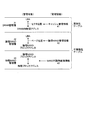
ここで、DRAM11の一時記憶領域111で管理される管理情報について説明する。図4は、メモリシステムで記憶されるデータを管理する層構造の一例を示す図である。なお、ここで、データとは、ホスト装置から書込要求/読出要求のあったデータのことをいうものとする。このメモリシステム10では、キャッシュの役割をするDRAM11でのデータ管理を行うDRAM管理層31と、NANDメモリ12での論理的なデータ管理を行う論理NAND管理層32と、NANDメモリ12での物理的なデータ管理やNANDメモリ12の延命処理などを行う物理NAND管理層33の3層構造でデータ管理が行われる。
Here, management information managed in the
DRAM11のライトキャッシュ領域WCとリードキャッシュ領域RCでは、ホスト装置のアドレス管理方法によって管理される論理アドレス(以下、LBA(Logical Block Address)という)で指定されたデータが、DRAM11上の所定の範囲の物理アドレス(以下、DRAM内物理アドレスという)に記憶される。また、DRAM管理層31内でのデータは、格納されるデータのLBAとDRAM内物理アドレスとの対応関係と、ページ中のセクタサイズ単位のデータの有無を示すセクタフラグと、を含むキャッシュ管理情報41によって管理される。
In the write cache area WC and the read cache area RC of the
図5は、キャッシュ管理情報テーブルの一例を示す図である。ここでは、キャッシュ管理情報41は、DRAM11の1ページサイズの領域1つに対して1エントリとし、エントリ数はライトキャッシュ領域WCとリードキャッシュ領域RCに収まるページ数以下とする。各エントリには、ページサイズのデータのLBAと、DRAM内物理アドレスと、このページをセクタサイズで分割した各領域における有効データの位置を示すセクタフラグと、が関連付けられている。
FIG. 5 is a diagram illustrating an example of the cache management information table. Here, the cache management information 41 has one entry for one page size area of the
NANDメモリ12では、DRAM11からのデータがNANDメモリ12上の所定の範囲の物理アドレス(以下、NAND内物理アドレスという)に格納される。多値メモリからなるNANDメモリ12では、書換可能回数に制約があるため、NANDメモリ12を構成する各ブロック間での書換回数が均等化するようにドライブ制御部14で制御されている。つまり、ドライブ制御部14は、NANDメモリ12内のあるNAND内物理アドレスに書込まれたデータの更新を行う場合に、そのデータが含まれるブロックのうち更新が必要な部分を反映させたデータを、元のブロックとは異なるブロックに書込み、元のブロックは無効化するようにして、NANDメモリ12を構成するブロック間での書換回数が均等化するように制御している。
In the
このように、NANDメモリ12では、データの書込/読出処理と消去処理とでは処理単位が異なるとともに、データの更新処理においては、更新前のデータの位置(ブロック)と更新後のデータの位置(ブロック)とが異なるため、この実施の形態では、NAND内物理アドレスのほかにNANDメモリ12内で独自に使用されるNAND内論理アドレス(以下、NAND内論理アドレスという)を設けることにする。
As described above, in the
そこで、論理NAND管理層32内でのデータは、DRAM11から受け取ったページサイズ単位のデータのLBAと、受け取ったデータを格納するNANDメモリ12の論理的なページ位置を示すNAND内論理アドレスとの間の関係と、NANDメモリ12における消去単位のブロック(以下、物理ブロックとする)とサイズが一致する論理的なブロック(以下、論理ブロックという)のアドレス範囲を示す関係と、を示す論理NAND管理情報42によって管理される。なお、物理ブロックを複数まとめたものを論理ブロックとしてもよい。また、物理NAND管理層33でのデータは、NANDメモリ12における論理ブロックのNAND内論理アドレスと、物理ブロックのNAND内物理アドレスとの対応関係を含むNAND内論理アドレス−物理アドレス変換情報(以下、論物変換情報という)43によって管理される。
Therefore, the data in the logical
図6は、論理NAND管理情報テーブルの一例を示す図であり、図7は、NAND内論物変換情報テーブルの一例を示す図である。図6に示されるように、論理NAND管理情報42は、論理ページ管理情報42aと論理ブロック管理情報42bとを含む。論理ページ管理情報42aは、1ページサイズの論理的な領域1つに対して1エントリとし、各エントリには、1ページサイズのデータのLBAと、NAND内論理アドレスと、このページが有効か否かを示すページフラグと、を含む。また、論理ブロック管理情報42bは、NANDメモリ12の1ブロックサイズの論理的な領域に対して設定されるNAND内論理アドレスを含む。また、図7に示されるように、NAND内論物変換情報43は、NANDメモリ12のNAND内物理アドレスとNAND内論理アドレスとが対応付けられている。
FIG. 6 is a diagram illustrating an example of a logical NAND management information table, and FIG. 7 is a diagram illustrating an example of a NAND intrinsic-physical conversion information table. As shown in FIG. 6, the logical
これらの管理情報によって、ホスト装置で使用されるLBAと、NANDメモリ12で使用されるNAND内論理アドレスと、NANDメモリ12で使用されるNAND内物理アドレスとの間を対応付けることができ、ホスト装置と当該メモリシステム10との間のデータのやり取りを行うことが可能となる。
With these management information, the LBA used in the host device, the logical address in the NAND used in the
なお、以下では、DRAM管理層31で管理される管理情報は、電源オフなどによって消失するので、揮発性テーブルともいい、論理NAND管理層32および物理NAND管理層33で管理される管理情報は、電源オフなどによって消失した際にメモリシステム10の次回起動時に支障を与え、保存しておくことが必要なので、不揮発性テーブルともいう。
In the following, the management information managed by the
この不揮発性テーブルは、NANDメモリ12に格納されているデータを管理するものであり、この不揮発性テーブルがなければNANDメモリ12に格納されている情報にアクセスできなかったり、既に記憶した領域内のデータを消してしまったりするので、不意の電源オフなどに備えて最新の情報に保存しておく必要がある。そのため、この実施の形態では、NANDメモリ12の管理情報保存領域126には、少なくとも不揮発性テーブルを含む管理情報を最新の状態で保存している。そこでつぎに、NANDメモリ12の管理情報保存領域126に保存される管理情報保存情報について説明する。なお、以下では、不揮発性テーブルのみを管理情報保存領域126に保存する場合を例に挙げる。
This non-volatile table manages the data stored in the
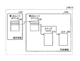
図8は、管理情報保存領域に記憶される管理情報保存情報の内容の一例を模式的に示す図である。この管理情報保存領域126には、ある時点における不揮発性テーブルの内容であるスナップショット210と、不揮発性テーブルの内容に変化があった場合に内容を変更した後の不揮発性テーブルとスナップショット210(またはスナップショット210と既に取られたログ)との差分情報であるログ220と、スナップショット210とこのスナップショット210に関する一番目に取得されたログ220の位置(ブロック)を示す第2のルートポインタ230と、第2のルートポインタ230が格納される位置(ブロック)を示す第1のルートポインタ240と、を含む管理情報保存情報が格納される。ここで、スナップショット210とは、DRAM11の一時記憶領域111に記憶される管理情報のうち、少なくとも不揮発性テーブルを含む管理情報を所定の時点で保存した情報のことをいう。
FIG. 8 is a diagram schematically illustrating an example of the contents of management information storage information stored in the management information storage area. In the management
この図8において、スナップショット210、ログ220、第2のルートポインタ230および第1のルートポインタ240は、それぞれ異なるブロックに格納される。なお、これらのスナップショット210、ログ220、第2のルートポインタ230および第1のルートポインタ240がそれぞれ格納されるブロックの大きさは、消去単位である物理ブロックと同じ大きさであるものとする。スナップショット210は、スナップショット格納用ブロックに格納される。スナップショット210には、NANDメモリ12の管理情報保存領域126内の不揮発性テーブルである論理NAND管理情報42とNAND内論物変換情報43とが含まれる。新しいスナップショット210が保存されると、以前に保存されていたスナップショット210とは別のブロックに保存される。
In FIG. 8, the snapshot 210, the
ログ220は、ログ格納用ブロックに格納される。このログ220は、スナップショットの世代が変わっても、同じログ格納用ブロックに連続して書込まれる。図9は、ログの一例を示す図である。ログ220は、変更対象の管理情報となる対象情報と、その対象情報中の変更対象となるエントリである対象エントリと、その対象エントリ中の変更対象となる項目である対象項目と、その対象項目の変更の内容である変更内容と、を含む。
The
第2のルートポインタ230は、第2のルートポインタ格納用ブロックに格納される。第2のルートポインタ230は、スナップショット210とログ220の格納位置を示すブロックの先頭アドレスを示すものであればよい。ただし、第2のルートポインタ230のうちスナップショット210の格納位置を示す部分は、スナップショット210に含まれる各管理情報(不揮発性テーブル)の先頭アドレスを示すものであってもよい。また、第2のルートポインタ230は、スナップショット210が新たに保存された場合に更新される。なお、ログ220のポインタは、第2のルートポインタ格納用ブロック内ではなく、スナップショット210の中に格納されていてもよい。
The
図10は、第2のルートポインタの一例を示す図である。1ブロックのサイズを512KBとすると、4KBのサイズの1ページに第2のルートポインタ230が格納される。この第2のルートポインタ230は、スナップショットアクセス情報と、ログアクセス情報と、ネクストポインタと、を含む。ここで、スナップショットアクセス情報は、スナップショットが格納されているブロックへアクセスするための情報である。また、ログアクセス情報は、ログが格納されているブロックへアクセスするための情報であり、ブロックを指定する情報と、基準となるスナップショットに関係するログが格納されている上記ブロック内の先頭ページを指定する情報と、を含む。ネクストポインタは、つぎの第2のルートポインタ230が格納されるページを示すインデックスである。このネクストポインタによって、第2のルートポインタ230はリンクドリスト方式の情報となり、第1のルートポインタ240で指示された第2のルートポインタ格納用ブロックの先頭ページからネクストポインタをたどることによって、最新の第2のルートポインタ230へとたどり着くことが可能となる。なお、リンクドリスト方式ではなく、第2のルートポインタ格納領域の先頭ページから第2のルートポインタ230を順に追記的に格納してもよい。
FIG. 10 is a diagram illustrating an example of the second route pointer. If the size of one block is 512 KB, the
第1のルートポインタ240は、第1のルートポインタ格納用ブロックに格納される。第1のルートポインタ240は、第2のルートポインタ230が格納されている第2のルートポインタ格納用ブロックのブロック(位置)へアクセスするための情報であり、メモリシステム10の起動時に、管理情報を復元するための処理の際に最初に読み込まれる情報である。この第1のルートポインタ240は、第2のルートポインタが格納されるブロックが変わった場合に変更される。第1のルートポインタ240は、第1のルートポインタ格納用ブロックに、たとえば、ブロックの先頭ページから順に追記的に格納される。このような場合には、第1のルートポインタ格納用ブロック内の未書込ページの1つ前のページが最新情報を有することになるので、未書込ページの最上位のページを検索することで、最新の第1のルートポインタ240を検索することができる。また、第2のルートポインタ230の場合のように、リンクドリストを用いることも可能である。
The
ここで、第1のルートポインタ240はNANDメモリ12内の固定領域1261に格納され、スナップショット210、ログ220および第2のルートポインタ230はNANDメモリ12内の可変領域1262に格納される。固定領域1261とは、NANDメモリ12において、論理NAND管理層32で管理される論理ブロックと、物理NAND管理層33で管理される物理ブロックとの関係が固定化している領域であり、書換えや書込みがほとんど発生しない更新頻度の低い、メモリシステム10を稼働させるのに必要な情報が格納される領域である。たとえば、現在書込み中のブロックがすべて満たされた場合には、管理情報保存領域126(NANDメモリ12)内の他のブロックに情報(第1のルートポインタ240)を書込むのではなく、ブロックの情報を消去した後に同じブロックの先頭ページから書込むように設定された領域である。また、この例では、NANDメモリ12は多値メモリで構成されるとしているが、第1のルートポインタ240のデータの信頼性を高めるために、2値モードで使用することが望ましい。
Here, the
一方の可変領域1262とは、固定領域1261を除くNANDメモリ12の領域において、論理NAND管理層32で管理される論理ブロックと、物理NAND管理層33で管理される物理ブロックとの関係が変化する領域である。たとえば、現在書込み中のブロックがすべて満たされた場合には、管理情報保存領域126内の可変領域1262中の書込可能なフリーブロックとなっている他のブロックにつぎの情報を書込むように設定された領域である。なお、この可変領域1262は、上記したようにNANDメモリ12中の固定領域1261を除いた領域であり、管理情報保存領域126中のスナップショット210、ログ220および第2のルートポインタ230が格納される領域のほかに、データ格納領域125も含まれる。つまり、固定領域1261を除いたNANDメモリ12中の物理的な領域を可変領域1262とし、この中で、データ格納領域125と管理情報保存領域126中のスナップショット210、ログ220および第2のルートポインタ230が格納される領域とが機能的に分離されている。
One
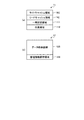
つぎに、ドライブ制御部14の機能について説明する。図11は、ドライブ制御部の機能構成の一例を示すブロック図である。ドライブ制御部14は、DRAM11−NANDメモリ12間のデータ転送やNANDメモリ12に関する各種機能の制御を行うデータ管理部141と、ATAインタフェースから受けた指示に基づいてデータ管理部141と協働してデータ転送処理を行うATAコマンド処理部142と、データ管理部141およびATAコマンド処理部142と協動して各種のセキュリティ情報を管理するセキュリティ管理部143と、電源オン時に、各管理プログラム(ファームウェア)をNANDメモリ12から図示しないメモリ(たとえば、SRAM(Static RAM))にロードするブートローダ144と、ドライブ制御部14内の各コントローラや回路の初期化を行う初期化管理部145と、外部からRS232Cインタフェースを介して供給されたデバッグ用データを処理するデバッグサポート部146と、を備える。
Next, functions of the
図12は、データ管理部の機能構成の一例を示すブロック図である。データ管理部141は、DRAM11とNANDメモリ12との間でデータ転送を行うデータ転送処理部151と、DRAM11およびNANDメモリ12に記憶されるデータの変更に伴って管理情報の変更や保存を行う管理情報管理部152と、電源オン時などにNANDメモリ12に保存された管理情報に基づいて最新の管理情報を復元する管理情報復元部155と、データや管理情報保存情報を書込むブロックの書換回数をNANDメモリ全体で均等化する書換ブロック均等化処理部156と、をさらに備える。
FIG. 12 is a block diagram illustrating an example of a functional configuration of the data management unit. The
また、管理情報管理部152は、管理情報書込部153と、管理情報保存部154と、をさらに備える。管理情報書込部153は、データ転送処理部151によるDRAM11またはNANDメモリ12で記憶されるデータの変更処理によって管理情報の更新が必要な場合に、DRAM11に記憶されている管理情報の更新を行う。
The management
管理情報保存部154は、メモリシステム10が所定の条件を満たしたとき、管理情報をスナップショット210として、または管理情報中の更新された分の情報をログ220として、NANDメモリ12の管理情報保存領域126に保存する。また、このスナップショット210またはログ220の保存に伴って第2のルートポインタ230または第2のルートポインタ230と第1のルートポインタ240が書込まれる位置が変更される場合には、この第2のルートポインタ230または第2のルートポインタ230と第1のルートポインタ240に対する更新処理も行う。
When the
管理情報保存部154によるスナップショット210は、NANDメモリ12の管理情報保存領域126中のログ220を記憶するために設けられたログ記憶領域が埋まってしまった(領域がデータで満杯になった)場合など、本メモリシステムの所定の条件に応じて実行される。
In the snapshot 210 by the management
また、管理情報保存部154によるログ220の保存は、DRAM11に記憶されている管理情報(不揮発性テーブル)の更新を伴うNANDメモリ12上のデータ更新時(NANDメモリ12へのデータ書込みが必要な場合)に行われる。
The
管理情報復元部155は、メモリシステム10に電源がオンされると、NANDメモリ12の管理情報保存領域126に保存されている管理情報保存情報に基づいた管理情報の復元処理を行う。具体的には、固定領域1261中の第1のルートポインタ240、可変領域1262中の第2のルートポインタ230、およびログ220へと順にたどっていき、最新のスナップショット210に対するログ220が存在するか否かを判定する。ログ220が存在しない場合には、スナップショット格納用ブロックのスナップショット210を管理情報としてDRAM11に復元する。また、ログ220が存在する場合には、瞬断などの異常終了であった場合であるので、スナップショット格納用ブロックからスナップショット210を取得し、ログ格納用ブロックからログ220を取得して、DRAM11上でスナップショット210にログ220を反映させて管理情報(不揮発性テーブル)の復元を行う。
When the
書換ブロック均等化処理部156は、NANDメモリ12中のデータ格納領域125中のブロックと、管理情報保存領域126中のスナップショット210、ログ220および第2のルートポインタ230が格納されるブロックとを、可変領域1262中の利用可能な他のブロックに書換えた場合に、可変領域1262中の各ブロックの書換可能回数が均等化するように、書換先のブロックを選択し、書換えを行うデータ転送処理部151や管理情報管理部152の管理情報保存部154に指示する。また、新たなブロックにデータやスナップショット210、ログ220および第2のルートポインタ230を書込む際にも、可変領域1262中の各ブロックの書換可能回数が均等化するように、書込先のブロックを選択し、書換えを行うデータ転送処理部151や管理情報管理部152の管理情報保存部154に指示する。この場合、可変領域1262中の利用可能なブロックであれば、そのブロックが過去にデータ格納領域125として使用されていたブロックであるか、管理情報保存領域126中のスナップショット210、ログ220および第2のルートポインタ230が格納されていたブロックであるか、を問わず、書込先のブロックを指定することができる。
The rewrite block
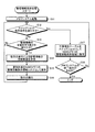
ここで、管理情報管理部152によるメモリシステム10の管理情報の保存処理について説明する。図13は、メモリシステムの管理情報の保存処理手順の一例を示すフローチャートである。なお、ここでは、メモリシステム10がホスト装置と接続され、ホスト装置の2次記憶装置として動作しているとともに、ホスト装置(メモリシステム10)が起動状態にあり、また、この起動状態の前のメモリシステム10の停止前にスナップショット210が保存されているものとする。
Here, the management information storage processing of the
まず、ホスト装置(メモリシステム10)の前回終了時に保存されたスナップショット210を基に、ホスト装置(メモリシステム10)が起動された状態にある(ステップS11)。ついで、管理情報管理部152は、上記所定のスナップショットの保存条件を満たすか否かを判定する(ステップS12)。スナップショット保存条件を満たさない場合(ステップS12でNoの場合)には、管理情報の更新を伴う指示(上記ログの保存条件を満たす指示)を受けたか否かを判定する(ステップS13)。管理情報の更新を伴う指示を受けなかった場合(ステップS13でNoの場合)には、ステップS12へと戻る。
First, the host device (memory system 10) is activated based on the snapshot 210 saved when the host device (memory system 10) ended last time (step S11). Next, the management
また、管理情報の更新を伴う指示(NANDメモリ12へのデータ書込み指示)を受けた場合(ステップS13でYesの場合)には、その指示を実行することによって管理情報がどのように更新されるか更新計画を決定し(ステップS14)、その更新計画をNANDメモリ12の管理情報保存領域126のログ格納用ブロックにログ220として保存する(ステップS15)。この更新計画(ログ)は、ログ格納用ブロックにログ220が格納されていない場合には、現時点の不揮発性テーブルとスナップショット格納用ブロックに保存されているスナップショット210との間の差分情報であり、ログ格納用ブロックにログ220(以下、過去ログという)が既に格納されている場合には、現時点の不揮発性テーブルと、スナップショット210と過去ログとを合わせたものとの間の差分情報である。なお、このログ220は、たとえば、ログ220(更新計画)をDRAM11上に記録した後、NANDメモリ12の管理情報保存領域126に保存される。
Further, when an instruction (instruction to write data to the NAND memory 12) accompanied with the update of the management information is received (Yes in step S13), how the management information is updated by executing the instruction. An update plan is determined (step S14), and the update plan is stored as a
ついで、論理NAND管理層は、ステップS13で受けた指示を実行する(ステップS16)。このような指示として、たとえばユーザデータのNANDメモリ12のデータ保存領域の所定のブロックへの書込処理が挙げられる。その後、再びステップS12へと戻る。
Next, the logical NAND management layer executes the instruction received in step S13 (step S16). An example of such an instruction is a process of writing user data to a predetermined block in the data storage area of the
また、ステップS12でスナップショット保存条件を満たす場合(ステップS12でYesの場合)には、DRAM11の一時記憶領域111内の少なくとも不揮発性テーブルを含む管理情報をスナップショット210としてNANDメモリ12の管理情報保存領域126に保存する(ステップS17)。そして、メモリシステム10の終了指示があるか否かを判定し(ステップS18)、終了指示がない場合(ステップS18でNoの場合)には再びステップS12へと戻り、終了指示がある場合(ステップS18でYesの場合)には、そのまま処理が終了する。
If the snapshot storage condition is satisfied in step S12 (Yes in step S12), the management information including at least the nonvolatile table in the
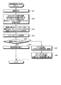
つぎに、管理情報復元部155によるメモリシステム10の管理情報の復元処理について説明する。図14は、メモリシステムの管理情報の復元処理手順の一例を示すフローチャートである。なお、ここでも、メモリシステム10がホスト装置と接続され、ホスト装置の2次記憶装置として動作しているものとする。
Next, the management information restoring process of the
まず、ホスト装置の電源がオンされ、メモリシステム10に対して起動指示が出されると(ステップS31)、管理情報復元部155は、NANDメモリ12の管理情報保存領域126中の最新の第1のルートポインタを読込み、第2のルートポインタ格納ブロックの位置を取得する(ステップS32)。ついで、スナップショット210とログ220が格納されているそれぞれのブロックのアドレスを取得し(ステップS33)、ステップS33で取得したNANDメモリ12中のアドレスからスナップショット210を読込み、DRAM11の一時記憶領域111に復元する(ステップ34)。
First, when the power of the host device is turned on and an activation instruction is issued to the memory system 10 (step S31), the management
その後、管理情報復元部155は、NANDメモリ12中のログ220を参照して、瞬断が発生したか否かを判定する(ステップS35)。瞬断が発生していない場合(ステップS35でNoの場合)には、ステップS34でDRAM11の一時記憶領域111に復元したスナップショット210から管理情報を復元し(ステップS36)、復元処理が終了する。
Thereafter, the management
一方、瞬断が発生した場合(ステップS35でYesの場合)には、ステップS33で取得したNANDメモリ12中のアドレスからログ220を取得してDRAM11の作業領域112に展開する(ステップS37)。そして、ステップS34でDRAM11の一時記憶領域111に復元したスナップショット210に対して、古いものから順にログ220を反映させて管理情報(不揮発性テーブル)を復元し(ステップS38)、管理情報の復元処理が終了する。
On the other hand, if an instantaneous interruption occurs (Yes in step S35), the
以上のように、本第1の実施の形態によれば、メモリシステム10の最新の管理情報であるスナップショット210とログ220の格納位置を示すポインタとして、スナップショット210とログ220の格納位置を示す第2のルートポインタ230を可変領域1262に設け、第2のルートポインタ230の格納位置を示す第1のルートポインタ240を固定領域1261に設けるように構成した。その結果、第1のルートポインタ240は、第2のルートポインタ格納用ブロックがすべて満たされるまで更新する必要がなく、第2のルートポインタ230の更新頻度に比べて著しく少なくすることができる。たとえば、第2のルートポインタ230を設けずに、第1のルートポインタ240をスナップショット210とログ220の格納位置を示すようにした場合には、スナップショット210が更新されるたびに第1のルートポインタ240が更新され、第1のルートポインタ格納用ブロックの消去回数が増えてしまう。これに対して、第2のルートポインタ230を設けることによって、スナップショット210が更新回数を、第2のルートポインタ230のページ数で割った数に抑えることができ、第1のルートポインタ格納用ブロックの消去回数を著しく減少させることができる。その結果、固定領域1261を構成するメモリセルトランジスタの寿命を延ばすことができるという効果を有する。また、第1のルートポインタ240の格納されている第1のルートポインタ格納用ブロックの書換回数を抑えることができるので、保存されているデータである第1のルートポインタ240の信頼性を高めることができるという効果も有する。
As described above, according to the first embodiment, the storage positions of the snapshot 210 and the
(第2の実施の形態)
第1の実施の形態において、第2のルートポインタおよび第1のルートポインタを多重化して保存することができる。
(Second Embodiment)
In the first embodiment, the second root pointer and the first root pointer can be multiplexed and stored.
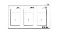
図15は、第1のルートポインタの多重化の一例を示す図である。ここでは、NANDメモリの管理情報保存領域の固定領域1261中の3つの異なるブロックに第1のルートポインタ240A〜240Cを保存している。この場合、第1のルートポインタの更新があった場合には、240A→240B→240Cの順にそれぞれのブロックへの書込みが行われる。また、第1のルートポインタ格納用ブロックが満杯になった場合には、このブロックを消去して新たな第2のルートポインタ格納用ブロックの位置を示す第1のルートポインタ240を、消去したブロックに書込む処理を行う。この場合にも、1つのブロックずつ順に消去と書込み処理を行う。このブロックの消去と書込み処理が行われる際に、第1のルートポインタ240A〜240Cを三重化することによって、第1のルートポインタ240が1つのブロックにしか格納されていない状態を短くすることができる。なお、ここでは、三重化する場合を示したが、二重化してもよいし、四重化以上の多重化を行ってもよい。四重化以上にすることで、第1のルートポインタ240を確実に二重化することができる。
FIG. 15 is a diagram illustrating an example of multiplexing of the first route pointer. Here, the
図16は、第2のルートポインタの多重化の一例を示す図である。この図16では、NANDメモリ12の管理情報保存領域126の可変領域1262中の2つの異なるブロックに第2のルートポインタ230A,230Bを保存している。
FIG. 16 is a diagram illustrating an example of multiplexing of the second route pointer. In FIG. 16, the
ここで、たとえば、これら2つの第2のルートポインタ230A,230Bを保存するブロックには、同じページ位置に同じ情報を保存するものとする。また、保存するタイミングとして、第2のルートポインタ230Aはスナップショットを保存する直前に保存し、第2のルートポインタ230Bはスナップショットの保存を終了した後に保存するものとする。このような保存規則を定めることによって、第2のルートポインタ230A、230Bが保存されるページ数が異なる場合には、瞬断が発生したものと判定することができ、瞬断時の起動処理をNANDメモリ12内のログ220を確認することなく行うことができる。なお、ここでは、二重化する場合を示したが、三重化以上の多重化を行ってもよい。
Here, for example, it is assumed that the same information is stored at the same page position in the block storing these two
また、第2のルートポインタ230を多重化する場合には、第1のルートポインタ240には、多重化したそれぞれの第2のルートポインタ230が格納されるブロックの位置を示す情報が格納される。
When the
この第2の実施の形態によれば、第1のルートポインタ240および第2のルートポインタを多重化することによって、それぞれの情報が消失してしまうことを防ぐことができるという効果を有する。
According to the second embodiment, by multiplexing the
なお、上述した説明では、電荷蓄積層は浮遊ゲート型に限らず、MONOS(Metal-Oxide-Nitride-Oxide-Semiconductor)構造のようなシリコン窒化膜を用いた電荷トラップ型やその他の方式であってもよい。 In the above description, the charge storage layer is not limited to the floating gate type, but is a charge trap type using a silicon nitride film such as a MONOS (Metal-Oxide-Nitride-Oxide-Semiconductor) structure or other methods. Also good.
10…メモリシステム、11…DRAM、12…NANDメモリ、13…電源回路、14…ドライブ制御部、15…バス、31…DRAM管理層、32…論理NAND管理層、33…物理NAND管理層、41…キャッシュ管理情報、42…管理情報、42b…論理ブロック管理情報、42a…論理ページ管理情報、43…NAND内論物変換情報、111…一時記憶領域、112…作業領域、125…データ格納領域、126…管理情報保存領域、141…データ管理部、151…データ転送処理部、152…管理情報管理部、153…管理情報書込部、154…管理情報保存部、155…管理情報復元部、156…書換ブロック均等化処理部、210…スナップショット、220…ログ、230,230A,230B…第2のルートポインタ、240,240A〜240C…第1のルートポインタ、1261…固定領域、1262…可変領域。
DESCRIPTION OF
Claims (3)
不揮発性の第2の記憶部と、
前記第1の記憶部を介してホスト装置と前記第2の記憶部との間のデータ転送を行うとともに、起動時に前記第2の記憶部に記憶された前記データの格納位置を含む管理情報を前記第1の記憶部に取込み、該取り込んだ管理情報を更新しながら管理情報に基づいて前記第1および第2の記憶部でのデータ管理を行うコントローラと、
を備え、
前記第2の記憶部は、前記第1の記憶部に取り込まれた最新の状態の管理情報、および該最新の状態の管理情報の保存位置を示す保存位置情報を含む管理情報保存情報を保存する管理情報保存領域を有し、
前記保存位置情報は、当該メモリシステムの起動時に前記コントローラによって読み込まれ、前記管理情報保存領域内の前記最新の状態の管理情報の格納位置を示す第2のポインタと、この第2のポインタの格納位置を示す第1のポインタとを含み、前記第1のポインタは前記第2の記憶部中の固定領域に格納され、前記第2のポインタは前記第2の記憶部中の前記固定領域を除いた領域に格納されることを特徴とするメモリシステム。 A volatile first storage unit;
A non-volatile second storage unit;
Management information including the storage location of the data stored in the second storage unit at the start-up is performed while transferring data between the host device and the second storage unit via the first storage unit. A controller that takes in the first storage unit and performs data management in the first and second storage units based on the management information while updating the taken-in management information;
With
The second storage unit stores management information storage information including management information in the latest state captured in the first storage unit and storage position information indicating a storage position of the management information in the latest state. It has a management information storage area,
The storage position information is read by the controller when the memory system is activated, and a second pointer indicating the storage position of the management information in the latest state in the management information storage area, and the storage of the second pointer A first pointer indicating a position, wherein the first pointer is stored in a fixed area in the second storage unit, and the second pointer excludes the fixed area in the second storage unit A memory system characterized by being stored in a separate area.
Priority Applications (10)
| Application Number | Priority Date | Filing Date | Title |
|---|---|---|---|
| JP2008051378A JP2009211202A (en) | 2008-02-29 | 2008-02-29 | Memory system |
| EP20100197364 EP2309392A1 (en) | 2008-02-29 | 2009-02-10 | Memory system |
| PCT/JP2009/052590 WO2009107506A1 (en) | 2008-02-29 | 2009-02-10 | Memory system |
| EP20090709441 EP2111583A4 (en) | 2008-02-29 | 2009-02-10 | Memory system |
| CN200980000132A CN101681313A (en) | 2008-02-29 | 2009-02-10 | Memory system |
| KR1020097017866A KR101103110B1 (en) | 2008-02-29 | 2009-02-10 | Memory system |
| US12/529,227 US8438343B2 (en) | 2008-02-29 | 2009-02-10 | Memory system with fixed and variable pointers |
| TW98105523A TWI418983B (en) | 2008-02-29 | 2009-02-20 | Memory system and method of controlling a memory system |
| US13/855,394 US8738867B2 (en) | 2008-02-29 | 2013-04-02 | Memory system |
| US14/226,510 US9043564B2 (en) | 2008-02-29 | 2014-03-26 | Memory system with fixed and variable pointers |
Applications Claiming Priority (1)
| Application Number | Priority Date | Filing Date | Title |
|---|---|---|---|
| JP2008051378A JP2009211202A (en) | 2008-02-29 | 2008-02-29 | Memory system |
Publications (1)
| Publication Number | Publication Date |
|---|---|
| JP2009211202A true JP2009211202A (en) | 2009-09-17 |
Family
ID=41115628
Family Applications (1)
| Application Number | Title | Priority Date | Filing Date |
|---|---|---|---|
| JP2008051378A Abandoned JP2009211202A (en) | 2008-02-29 | 2008-02-29 | Memory system |
Country Status (1)
| Country | Link |
|---|---|
| JP (1) | JP2009211202A (en) |
Cited By (2)
| Publication number | Priority date | Publication date | Assignee | Title |
|---|---|---|---|---|
| US8527733B2 (en) | 2010-12-15 | 2013-09-03 | Kabushiki Kaisha Toshiba | Memory system |
| JP2016105320A (en) * | 2010-09-28 | 2016-06-09 | ピュア・ストレージ・インコーポレイテッド | Adaptive RAID for SSD environment |
Citations (1)
| Publication number | Priority date | Publication date | Assignee | Title |
|---|---|---|---|---|
| JP2006285600A (en) * | 2005-03-31 | 2006-10-19 | Tokyo Electron Device Ltd | Storage, memory management device, memory management method, and program |
-
2008
- 2008-02-29 JP JP2008051378A patent/JP2009211202A/en not_active Abandoned
Patent Citations (1)
| Publication number | Priority date | Publication date | Assignee | Title |
|---|---|---|---|---|
| JP2006285600A (en) * | 2005-03-31 | 2006-10-19 | Tokyo Electron Device Ltd | Storage, memory management device, memory management method, and program |
Cited By (2)
| Publication number | Priority date | Publication date | Assignee | Title |
|---|---|---|---|---|
| JP2016105320A (en) * | 2010-09-28 | 2016-06-09 | ピュア・ストレージ・インコーポレイテッド | Adaptive RAID for SSD environment |
| US8527733B2 (en) | 2010-12-15 | 2013-09-03 | Kabushiki Kaisha Toshiba | Memory system |
Similar Documents
| Publication | Publication Date | Title |
|---|---|---|
| US11573712B2 (en) | Memory system storing management information and method of controlling same | |
| KR101103110B1 (en) | Memory system | |
| US8285954B2 (en) | Memory system managing a plurality of logs | |
| JP4675984B2 (en) | Memory system | |
| JP2009205555A (en) | Memory system | |
| KR101102155B1 (en) | Memory system | |
| JP2010152514A (en) | Memory system | |
| JP2009211202A (en) | Memory system | |
| JP4551938B2 (en) | Memory system | |
| JP4558052B2 (en) | Memory system | |
| JP2009211196A (en) | Memory system | |
| JP4551939B2 (en) | Memory system | |
| JP2009211188A (en) | Memory system | |
| JP2009211213A (en) | Memory system | |
| JP2009211218A (en) | Memory system and hit judgment method |
Legal Events
| Date | Code | Title | Description |
|---|---|---|---|
| A621 | Written request for application examination |
Free format text: JAPANESE INTERMEDIATE CODE: A621 Effective date: 20100218 |
|
| A01 | Written decision to grant a patent or to grant a registration (utility model) |
Free format text: JAPANESE INTERMEDIATE CODE: A01 Effective date: 20120508 |
|
| A762 | Written abandonment of application |
Free format text: JAPANESE INTERMEDIATE CODE: A762 Effective date: 20120607 |