JP2009200483A - Method for forming silicon oxide film - Google Patents
Method for forming silicon oxide film Download PDFInfo
- Publication number
- JP2009200483A JP2009200483A JP2009013724A JP2009013724A JP2009200483A JP 2009200483 A JP2009200483 A JP 2009200483A JP 2009013724 A JP2009013724 A JP 2009013724A JP 2009013724 A JP2009013724 A JP 2009013724A JP 2009200483 A JP2009200483 A JP 2009200483A
- Authority
- JP
- Japan
- Prior art keywords
- silicon oxide
- oxide film
- plasma
- processing
- thickness
- Prior art date
- Legal status (The legal status is an assumption and is not a legal conclusion. Google has not performed a legal analysis and makes no representation as to the accuracy of the status listed.)
- Pending
Links
- VYPSYNLAJGMNEJ-UHFFFAOYSA-N Silicium dioxide Chemical compound O=[Si]=O VYPSYNLAJGMNEJ-UHFFFAOYSA-N 0.000 title claims abstract description 143
- 229910052814 silicon oxide Inorganic materials 0.000 title claims abstract description 137
- 238000000034 method Methods 0.000 title claims description 111
- 238000012545 processing Methods 0.000 claims abstract description 170
- 239000007789 gas Substances 0.000 claims abstract description 117
- 238000007254 oxidation reaction Methods 0.000 claims abstract description 115
- 230000003647 oxidation Effects 0.000 claims abstract description 114
- 229910052760 oxygen Inorganic materials 0.000 claims abstract description 47
- 239000001301 oxygen Substances 0.000 claims abstract description 46
- QVGXLLKOCUKJST-UHFFFAOYSA-N atomic oxygen Chemical compound [O] QVGXLLKOCUKJST-UHFFFAOYSA-N 0.000 claims abstract description 43
- 229910052710 silicon Inorganic materials 0.000 claims abstract description 42
- 239000010703 silicon Substances 0.000 claims abstract description 42
- 230000008569 process Effects 0.000 claims description 58
- XUIMIQQOPSSXEZ-UHFFFAOYSA-N Silicon Chemical compound [Si] XUIMIQQOPSSXEZ-UHFFFAOYSA-N 0.000 claims description 40
- 230000007246 mechanism Effects 0.000 claims description 25
- UFHFLCQGNIYNRP-UHFFFAOYSA-N Hydrogen Chemical compound [H][H] UFHFLCQGNIYNRP-UHFFFAOYSA-N 0.000 claims description 19
- 230000015572 biosynthetic process Effects 0.000 claims description 18
- 239000001257 hydrogen Substances 0.000 claims description 15
- 229910052739 hydrogen Inorganic materials 0.000 claims description 15
- 238000003860 storage Methods 0.000 claims description 10
- 230000005855 radiation Effects 0.000 abstract description 15
- 230000001788 irregular Effects 0.000 abstract description 4
- 239000010408 film Substances 0.000 description 226
- 239000000758 substrate Substances 0.000 description 30
- 238000005530 etching Methods 0.000 description 23
- 229910021420 polycrystalline silicon Inorganic materials 0.000 description 21
- 229920005591 polysilicon Polymers 0.000 description 20
- 239000010410 layer Substances 0.000 description 18
- 150000002500 ions Chemical class 0.000 description 14
- 230000000052 comparative effect Effects 0.000 description 12
- 239000000463 material Substances 0.000 description 12
- 229910052751 metal Inorganic materials 0.000 description 12
- 239000002184 metal Substances 0.000 description 12
- 230000005540 biological transmission Effects 0.000 description 11
- 229910052581 Si3N4 Inorganic materials 0.000 description 10
- HQVNEWCFYHHQES-UHFFFAOYSA-N silicon nitride Chemical compound N12[Si]34N5[Si]62N3[Si]51N64 HQVNEWCFYHHQES-UHFFFAOYSA-N 0.000 description 10
- 229910004298 SiO 2 Inorganic materials 0.000 description 8
- 239000011261 inert gas Substances 0.000 description 8
- 238000004519 manufacturing process Methods 0.000 description 8
- -1 A1 2 0 3 Substances 0.000 description 7
- 239000010453 quartz Substances 0.000 description 6
- 238000005229 chemical vapour deposition Methods 0.000 description 5
- 239000004020 conductor Substances 0.000 description 5
- 230000001590 oxidative effect Effects 0.000 description 5
- MYMOFIZGZYHOMD-UHFFFAOYSA-N Dioxygen Chemical compound O=O MYMOFIZGZYHOMD-UHFFFAOYSA-N 0.000 description 4
- MWUXSHHQAYIFBG-UHFFFAOYSA-N Nitric oxide Chemical compound O=[N] MWUXSHHQAYIFBG-UHFFFAOYSA-N 0.000 description 4
- 229910001882 dioxygen Inorganic materials 0.000 description 4
- 238000002955 isolation Methods 0.000 description 4
- 239000004065 semiconductor Substances 0.000 description 4
- 230000009471 action Effects 0.000 description 3
- 229910052782 aluminium Inorganic materials 0.000 description 3
- XAGFODPZIPBFFR-UHFFFAOYSA-N aluminium Chemical compound [Al] XAGFODPZIPBFFR-UHFFFAOYSA-N 0.000 description 3
- 239000000919 ceramic Substances 0.000 description 3
- 239000000498 cooling water Substances 0.000 description 3
- 238000013461 design Methods 0.000 description 3
- 238000010438 heat treatment Methods 0.000 description 3
- 229910021421 monocrystalline silicon Inorganic materials 0.000 description 3
- 238000001020 plasma etching Methods 0.000 description 3
- 238000005498 polishing Methods 0.000 description 3
- 230000000644 propagated effect Effects 0.000 description 3
- 238000012360 testing method Methods 0.000 description 3
- XKRFYHLGVUSROY-UHFFFAOYSA-N Argon Chemical compound [Ar] XKRFYHLGVUSROY-UHFFFAOYSA-N 0.000 description 2
- PXHVJJICTQNCMI-UHFFFAOYSA-N Nickel Chemical compound [Ni] PXHVJJICTQNCMI-UHFFFAOYSA-N 0.000 description 2
- GQPLMRYTRLFLPF-UHFFFAOYSA-N Nitrous Oxide Chemical compound [O-][N+]#N GQPLMRYTRLFLPF-UHFFFAOYSA-N 0.000 description 2
- 229910021417 amorphous silicon Inorganic materials 0.000 description 2
- 238000004380 ashing Methods 0.000 description 2
- 238000004140 cleaning Methods 0.000 description 2
- 230000003247 decreasing effect Effects 0.000 description 2
- 230000005672 electromagnetic field Effects 0.000 description 2
- 230000005284 excitation Effects 0.000 description 2
- 230000006870 function Effects 0.000 description 2
- 229910052736 halogen Inorganic materials 0.000 description 2
- 150000002366 halogen compounds Chemical class 0.000 description 2
- 150000002367 halogens Chemical class 0.000 description 2
- 150000002431 hydrogen Chemical class 0.000 description 2
- 239000012535 impurity Substances 0.000 description 2
- 238000000206 photolithography Methods 0.000 description 2
- 229920002120 photoresistant polymer Polymers 0.000 description 2
- 230000001737 promoting effect Effects 0.000 description 2
- 230000008439 repair process Effects 0.000 description 2
- 239000000126 substance Substances 0.000 description 2
- 239000010409 thin film Substances 0.000 description 2
- XLYOFNOQVPJJNP-UHFFFAOYSA-N water Chemical compound O XLYOFNOQVPJJNP-UHFFFAOYSA-N 0.000 description 2
- RYGMFSIKBFXOCR-UHFFFAOYSA-N Copper Chemical compound [Cu] RYGMFSIKBFXOCR-UHFFFAOYSA-N 0.000 description 1
- ZOKXTWBITQBERF-UHFFFAOYSA-N Molybdenum Chemical compound [Mo] ZOKXTWBITQBERF-UHFFFAOYSA-N 0.000 description 1
- 229910004541 SiN Inorganic materials 0.000 description 1
- BQCADISMDOOEFD-UHFFFAOYSA-N Silver Chemical compound [Ag] BQCADISMDOOEFD-UHFFFAOYSA-N 0.000 description 1
- 229910052783 alkali metal Inorganic materials 0.000 description 1
- 150000001340 alkali metals Chemical class 0.000 description 1
- 229910045601 alloy Inorganic materials 0.000 description 1
- 239000000956 alloy Substances 0.000 description 1
- 229910052786 argon Inorganic materials 0.000 description 1
- 230000008901 benefit Effects 0.000 description 1
- 229910052802 copper Inorganic materials 0.000 description 1
- 239000010949 copper Substances 0.000 description 1
- 239000003989 dielectric material Substances 0.000 description 1
- 230000000694 effects Effects 0.000 description 1
- 230000005684 electric field Effects 0.000 description 1
- PCHJSUWPFVWCPO-UHFFFAOYSA-N gold Chemical group [Au] PCHJSUWPFVWCPO-UHFFFAOYSA-N 0.000 description 1
- 229910052737 gold Inorganic materials 0.000 description 1
- 239000010931 gold Substances 0.000 description 1
- 239000011229 interlayer Substances 0.000 description 1
- 239000007769 metal material Substances 0.000 description 1
- 238000012986 modification Methods 0.000 description 1
- 230000004048 modification Effects 0.000 description 1
- 229910052750 molybdenum Inorganic materials 0.000 description 1
- 239000011733 molybdenum Substances 0.000 description 1
- 229910052759 nickel Inorganic materials 0.000 description 1
- 229960001730 nitrous oxide Drugs 0.000 description 1
- 235000013842 nitrous oxide Nutrition 0.000 description 1
- 238000000059 patterning Methods 0.000 description 1
- 230000002093 peripheral effect Effects 0.000 description 1
- 238000005268 plasma chemical vapour deposition Methods 0.000 description 1
- 238000009832 plasma treatment Methods 0.000 description 1
- 229920001721 polyimide Polymers 0.000 description 1
- 239000009719 polyimide resin Substances 0.000 description 1
- 229920001343 polytetrafluoroethylene Polymers 0.000 description 1
- 239000004810 polytetrafluoroethylene Substances 0.000 description 1
- 230000001902 propagating effect Effects 0.000 description 1
- 238000010926 purge Methods 0.000 description 1
- 239000011347 resin Substances 0.000 description 1
- 229920005989 resin Polymers 0.000 description 1
- 238000007789 sealing Methods 0.000 description 1
- 238000004904 shortening Methods 0.000 description 1
- 229910052709 silver Inorganic materials 0.000 description 1
- 239000004332 silver Substances 0.000 description 1
- 239000010935 stainless steel Substances 0.000 description 1
- 229910001220 stainless steel Inorganic materials 0.000 description 1
- 230000008646 thermal stress Effects 0.000 description 1
- 238000012546 transfer Methods 0.000 description 1
- WFKWXMTUELFFGS-UHFFFAOYSA-N tungsten Chemical compound [W] WFKWXMTUELFFGS-UHFFFAOYSA-N 0.000 description 1
- 229910052721 tungsten Inorganic materials 0.000 description 1
- 239000010937 tungsten Substances 0.000 description 1
- 238000009279 wet oxidation reaction Methods 0.000 description 1
Images


Classifications
-
- H—ELECTRICITY
- H01—ELECTRIC ELEMENTS
- H01L—SEMICONDUCTOR DEVICES NOT COVERED BY CLASS H10
- H01L21/00—Processes or apparatus adapted for the manufacture or treatment of semiconductor or solid state devices or of parts thereof
- H01L21/02—Manufacture or treatment of semiconductor devices or of parts thereof
- H01L21/02104—Forming layers
- H01L21/02107—Forming insulating materials on a substrate
- H01L21/02225—Forming insulating materials on a substrate characterised by the process for the formation of the insulating layer
- H01L21/0226—Forming insulating materials on a substrate characterised by the process for the formation of the insulating layer formation by a deposition process
- H01L21/02263—Forming insulating materials on a substrate characterised by the process for the formation of the insulating layer formation by a deposition process deposition from the gas or vapour phase
- H01L21/02271—Forming insulating materials on a substrate characterised by the process for the formation of the insulating layer formation by a deposition process deposition from the gas or vapour phase deposition by decomposition or reaction of gaseous or vapour phase compounds, i.e. chemical vapour deposition
- H01L21/02274—Forming insulating materials on a substrate characterised by the process for the formation of the insulating layer formation by a deposition process deposition from the gas or vapour phase deposition by decomposition or reaction of gaseous or vapour phase compounds, i.e. chemical vapour deposition in the presence of a plasma [PECVD]
-
- H—ELECTRICITY
- H01—ELECTRIC ELEMENTS
- H01J—ELECTRIC DISCHARGE TUBES OR DISCHARGE LAMPS
- H01J37/00—Discharge tubes with provision for introducing objects or material to be exposed to the discharge, e.g. for the purpose of examination or processing thereof
- H01J37/32—Gas-filled discharge tubes
- H01J37/32009—Arrangements for generation of plasma specially adapted for examination or treatment of objects, e.g. plasma sources
- H01J37/32192—Microwave generated discharge
- H01J37/32211—Means for coupling power to the plasma
- H01J37/3222—Antennas
-
- H—ELECTRICITY
- H01—ELECTRIC ELEMENTS
- H01L—SEMICONDUCTOR DEVICES NOT COVERED BY CLASS H10
- H01L21/00—Processes or apparatus adapted for the manufacture or treatment of semiconductor or solid state devices or of parts thereof
- H01L21/02—Manufacture or treatment of semiconductor devices or of parts thereof
- H01L21/02104—Forming layers
- H01L21/02107—Forming insulating materials on a substrate
- H01L21/02109—Forming insulating materials on a substrate characterised by the type of layer, e.g. type of material, porous/non-porous, pre-cursors, mixtures or laminates
- H01L21/02112—Forming insulating materials on a substrate characterised by the type of layer, e.g. type of material, porous/non-porous, pre-cursors, mixtures or laminates characterised by the material of the layer
- H01L21/02123—Forming insulating materials on a substrate characterised by the type of layer, e.g. type of material, porous/non-porous, pre-cursors, mixtures or laminates characterised by the material of the layer the material containing silicon
- H01L21/02164—Forming insulating materials on a substrate characterised by the type of layer, e.g. type of material, porous/non-porous, pre-cursors, mixtures or laminates characterised by the material of the layer the material containing silicon the material being a silicon oxide, e.g. SiO2
-
- H—ELECTRICITY
- H01—ELECTRIC ELEMENTS
- H01L—SEMICONDUCTOR DEVICES NOT COVERED BY CLASS H10
- H01L21/00—Processes or apparatus adapted for the manufacture or treatment of semiconductor or solid state devices or of parts thereof
- H01L21/02—Manufacture or treatment of semiconductor devices or of parts thereof
- H01L21/02104—Forming layers
- H01L21/02107—Forming insulating materials on a substrate
- H01L21/02225—Forming insulating materials on a substrate characterised by the process for the formation of the insulating layer
- H01L21/02227—Forming insulating materials on a substrate characterised by the process for the formation of the insulating layer formation by a process other than a deposition process
- H01L21/0223—Forming insulating materials on a substrate characterised by the process for the formation of the insulating layer formation by a process other than a deposition process formation by oxidation, e.g. oxidation of the substrate
- H01L21/02233—Forming insulating materials on a substrate characterised by the process for the formation of the insulating layer formation by a process other than a deposition process formation by oxidation, e.g. oxidation of the substrate of the semiconductor substrate or a semiconductor layer
- H01L21/02236—Forming insulating materials on a substrate characterised by the process for the formation of the insulating layer formation by a process other than a deposition process formation by oxidation, e.g. oxidation of the substrate of the semiconductor substrate or a semiconductor layer group IV semiconductor
- H01L21/02238—Forming insulating materials on a substrate characterised by the process for the formation of the insulating layer formation by a process other than a deposition process formation by oxidation, e.g. oxidation of the substrate of the semiconductor substrate or a semiconductor layer group IV semiconductor silicon in uncombined form, i.e. pure silicon
-
- H—ELECTRICITY
- H01—ELECTRIC ELEMENTS
- H01L—SEMICONDUCTOR DEVICES NOT COVERED BY CLASS H10
- H01L21/00—Processes or apparatus adapted for the manufacture or treatment of semiconductor or solid state devices or of parts thereof
- H01L21/02—Manufacture or treatment of semiconductor devices or of parts thereof
- H01L21/04—Manufacture or treatment of semiconductor devices or of parts thereof the devices having at least one potential-jump barrier or surface barrier, e.g. PN junction, depletion layer or carrier concentration layer
- H01L21/18—Manufacture or treatment of semiconductor devices or of parts thereof the devices having at least one potential-jump barrier or surface barrier, e.g. PN junction, depletion layer or carrier concentration layer the devices having semiconductor bodies comprising elements of Group IV of the Periodic System or AIIIBV compounds with or without impurities, e.g. doping materials
- H01L21/28—Manufacture of electrodes on semiconductor bodies using processes or apparatus not provided for in groups H01L21/20 - H01L21/268
- H01L21/28008—Making conductor-insulator-semiconductor electrodes
- H01L21/28017—Making conductor-insulator-semiconductor electrodes the insulator being formed after the semiconductor body, the semiconductor being silicon
- H01L21/28158—Making the insulator
- H01L21/28167—Making the insulator on single crystalline silicon, e.g. using a liquid, i.e. chemical oxidation
- H01L21/28211—Making the insulator on single crystalline silicon, e.g. using a liquid, i.e. chemical oxidation in a gaseous ambient using an oxygen or a water vapour, e.g. RTO, possibly through a layer
-
- H—ELECTRICITY
- H01—ELECTRIC ELEMENTS
- H01L—SEMICONDUCTOR DEVICES NOT COVERED BY CLASS H10
- H01L21/00—Processes or apparatus adapted for the manufacture or treatment of semiconductor or solid state devices or of parts thereof
- H01L21/02—Manufacture or treatment of semiconductor devices or of parts thereof
- H01L21/04—Manufacture or treatment of semiconductor devices or of parts thereof the devices having at least one potential-jump barrier or surface barrier, e.g. PN junction, depletion layer or carrier concentration layer
- H01L21/18—Manufacture or treatment of semiconductor devices or of parts thereof the devices having at least one potential-jump barrier or surface barrier, e.g. PN junction, depletion layer or carrier concentration layer the devices having semiconductor bodies comprising elements of Group IV of the Periodic System or AIIIBV compounds with or without impurities, e.g. doping materials
- H01L21/30—Treatment of semiconductor bodies using processes or apparatus not provided for in groups H01L21/20 - H01L21/26
- H01L21/31—Treatment of semiconductor bodies using processes or apparatus not provided for in groups H01L21/20 - H01L21/26 to form insulating layers thereon, e.g. for masking or by using photolithographic techniques; After treatment of these layers; Selection of materials for these layers
- H01L21/314—Inorganic layers
- H01L21/316—Inorganic layers composed of oxides or glassy oxides or oxide based glass
- H01L21/3165—Inorganic layers composed of oxides or glassy oxides or oxide based glass formed by oxidation
- H01L21/31654—Inorganic layers composed of oxides or glassy oxides or oxide based glass formed by oxidation of semiconductor materials, e.g. the body itself
- H01L21/31658—Inorganic layers composed of oxides or glassy oxides or oxide based glass formed by oxidation of semiconductor materials, e.g. the body itself by thermal oxidation, e.g. of SiGe
- H01L21/31662—Inorganic layers composed of oxides or glassy oxides or oxide based glass formed by oxidation of semiconductor materials, e.g. the body itself by thermal oxidation, e.g. of SiGe of silicon in uncombined form
-
- H—ELECTRICITY
- H01—ELECTRIC ELEMENTS
- H01L—SEMICONDUCTOR DEVICES NOT COVERED BY CLASS H10
- H01L21/00—Processes or apparatus adapted for the manufacture or treatment of semiconductor or solid state devices or of parts thereof
- H01L21/02—Manufacture or treatment of semiconductor devices or of parts thereof
- H01L21/04—Manufacture or treatment of semiconductor devices or of parts thereof the devices having at least one potential-jump barrier or surface barrier, e.g. PN junction, depletion layer or carrier concentration layer
- H01L21/18—Manufacture or treatment of semiconductor devices or of parts thereof the devices having at least one potential-jump barrier or surface barrier, e.g. PN junction, depletion layer or carrier concentration layer the devices having semiconductor bodies comprising elements of Group IV of the Periodic System or AIIIBV compounds with or without impurities, e.g. doping materials
- H01L21/30—Treatment of semiconductor bodies using processes or apparatus not provided for in groups H01L21/20 - H01L21/26
- H01L21/31—Treatment of semiconductor bodies using processes or apparatus not provided for in groups H01L21/20 - H01L21/26 to form insulating layers thereon, e.g. for masking or by using photolithographic techniques; After treatment of these layers; Selection of materials for these layers
- H01L21/3205—Deposition of non-insulating-, e.g. conductive- or resistive-, layers on insulating layers; After-treatment of these layers
- H01L21/321—After treatment
- H01L21/32105—Oxidation of silicon-containing layers
-
- H—ELECTRICITY
- H01—ELECTRIC ELEMENTS
- H01L—SEMICONDUCTOR DEVICES NOT COVERED BY CLASS H10
- H01L21/00—Processes or apparatus adapted for the manufacture or treatment of semiconductor or solid state devices or of parts thereof
- H01L21/70—Manufacture or treatment of devices consisting of a plurality of solid state components formed in or on a common substrate or of parts thereof; Manufacture of integrated circuit devices or of parts thereof
- H01L21/71—Manufacture of specific parts of devices defined in group H01L21/70
- H01L21/76—Making of isolation regions between components
- H01L21/762—Dielectric regions, e.g. EPIC dielectric isolation, LOCOS; Trench refilling techniques, SOI technology, use of channel stoppers
- H01L21/76224—Dielectric regions, e.g. EPIC dielectric isolation, LOCOS; Trench refilling techniques, SOI technology, use of channel stoppers using trench refilling with dielectric materials
- H01L21/76232—Dielectric regions, e.g. EPIC dielectric isolation, LOCOS; Trench refilling techniques, SOI technology, use of channel stoppers using trench refilling with dielectric materials of trenches having a shape other than rectangular or V-shape, e.g. rounded corners, oblique or rounded trench walls
- H01L21/76235—Dielectric regions, e.g. EPIC dielectric isolation, LOCOS; Trench refilling techniques, SOI technology, use of channel stoppers using trench refilling with dielectric materials of trenches having a shape other than rectangular or V-shape, e.g. rounded corners, oblique or rounded trench walls trench shape altered by a local oxidation of silicon process step, e.g. trench corner rounding by LOCOS
-
- H—ELECTRICITY
- H01—ELECTRIC ELEMENTS
- H01L—SEMICONDUCTOR DEVICES NOT COVERED BY CLASS H10
- H01L29/00—Semiconductor devices adapted for rectifying, amplifying, oscillating or switching, or capacitors or resistors with at least one potential-jump barrier or surface barrier, e.g. PN junction depletion layer or carrier concentration layer; Details of semiconductor bodies or of electrodes thereof ; Multistep manufacturing processes therefor
- H01L29/40—Electrodes ; Multistep manufacturing processes therefor
- H01L29/41—Electrodes ; Multistep manufacturing processes therefor characterised by their shape, relative sizes or dispositions
- H01L29/423—Electrodes ; Multistep manufacturing processes therefor characterised by their shape, relative sizes or dispositions not carrying the current to be rectified, amplified or switched
- H01L29/42312—Gate electrodes for field effect devices
- H01L29/42316—Gate electrodes for field effect devices for field-effect transistors
- H01L29/4232—Gate electrodes for field effect devices for field-effect transistors with insulated gate
- H01L29/42372—Gate electrodes for field effect devices for field-effect transistors with insulated gate characterised by the conducting layer, e.g. the length, the sectional shape or the lay-out
-
- H—ELECTRICITY
- H01—ELECTRIC ELEMENTS
- H01L—SEMICONDUCTOR DEVICES NOT COVERED BY CLASS H10
- H01L29/00—Semiconductor devices adapted for rectifying, amplifying, oscillating or switching, or capacitors or resistors with at least one potential-jump barrier or surface barrier, e.g. PN junction depletion layer or carrier concentration layer; Details of semiconductor bodies or of electrodes thereof ; Multistep manufacturing processes therefor
- H01L29/66—Types of semiconductor device ; Multistep manufacturing processes therefor
- H01L29/68—Types of semiconductor device ; Multistep manufacturing processes therefor controllable by only the electric current supplied, or only the electric potential applied, to an electrode which does not carry the current to be rectified, amplified or switched
- H01L29/76—Unipolar devices, e.g. field effect transistors
- H01L29/772—Field effect transistors
- H01L29/78—Field effect transistors with field effect produced by an insulated gate
- H01L29/788—Field effect transistors with field effect produced by an insulated gate with floating gate
- H01L29/7881—Programmable transistors with only two possible levels of programmation
-
- H—ELECTRICITY
- H10—SEMICONDUCTOR DEVICES; ELECTRIC SOLID-STATE DEVICES NOT OTHERWISE PROVIDED FOR
- H10B—ELECTRONIC MEMORY DEVICES
- H10B41/00—Electrically erasable-and-programmable ROM [EEPROM] devices comprising floating gates
- H10B41/30—Electrically erasable-and-programmable ROM [EEPROM] devices comprising floating gates characterised by the memory core region
-
- H—ELECTRICITY
- H01—ELECTRIC ELEMENTS
- H01L—SEMICONDUCTOR DEVICES NOT COVERED BY CLASS H10
- H01L21/00—Processes or apparatus adapted for the manufacture or treatment of semiconductor or solid state devices or of parts thereof
- H01L21/70—Manufacture or treatment of devices consisting of a plurality of solid state components formed in or on a common substrate or of parts thereof; Manufacture of integrated circuit devices or of parts thereof
- H01L21/77—Manufacture or treatment of devices consisting of a plurality of solid state components or integrated circuits formed in, or on, a common substrate
- H01L21/78—Manufacture or treatment of devices consisting of a plurality of solid state components or integrated circuits formed in, or on, a common substrate with subsequent division of the substrate into plural individual devices
- H01L21/82—Manufacture or treatment of devices consisting of a plurality of solid state components or integrated circuits formed in, or on, a common substrate with subsequent division of the substrate into plural individual devices to produce devices, e.g. integrated circuits, each consisting of a plurality of components
- H01L21/822—Manufacture or treatment of devices consisting of a plurality of solid state components or integrated circuits formed in, or on, a common substrate with subsequent division of the substrate into plural individual devices to produce devices, e.g. integrated circuits, each consisting of a plurality of components the substrate being a semiconductor, using silicon technology
- H01L21/8232—Field-effect technology
- H01L21/8234—MIS technology, i.e. integration processes of field effect transistors of the conductor-insulator-semiconductor type
- H01L21/823468—MIS technology, i.e. integration processes of field effect transistors of the conductor-insulator-semiconductor type with a particular manufacturing method of the gate sidewall spacers, e.g. double spacers, particular spacer material or shape
Landscapes
- Engineering & Computer Science (AREA)
- Physics & Mathematics (AREA)
- Microelectronics & Electronic Packaging (AREA)
- Power Engineering (AREA)
- Condensed Matter Physics & Semiconductors (AREA)
- General Physics & Mathematics (AREA)
- Computer Hardware Design (AREA)
- Manufacturing & Machinery (AREA)
- Chemical & Material Sciences (AREA)
- Plasma & Fusion (AREA)
- Ceramic Engineering (AREA)
- Analytical Chemistry (AREA)
- Chemical Kinetics & Catalysis (AREA)
- Crystallography & Structural Chemistry (AREA)
- General Chemical & Material Sciences (AREA)
- Formation Of Insulating Films (AREA)
- Drying Of Semiconductors (AREA)
- Plasma Technology (AREA)
- Element Separation (AREA)
- Metal-Oxide And Bipolar Metal-Oxide Semiconductor Integrated Circuits (AREA)
- Semiconductor Memories (AREA)
- Non-Volatile Memory (AREA)
- Electrodes Of Semiconductors (AREA)
Abstract
Description
本発明は、シリコン酸化膜の形成方法に関し、詳細には、例えば、半導体装置の製造過程でシリコンに形成されたトレンチ内を酸化したり、トランジスタのゲート電極をエッチングにより形成した後でライン&スペースの凹凸パターンに酸化処理を行ったりする場合に適用可能なシリコン酸化膜の形成方法に関する。 The present invention relates to a method of forming a silicon oxide film, and more specifically, for example, a line and space after a trench formed in silicon is oxidized in a manufacturing process of a semiconductor device or a gate electrode of a transistor is formed by etching. The present invention relates to a method for forming a silicon oxide film that can be applied when an oxidization process is performed on the uneven pattern.
シリコン基板上に形成される素子を電気的に分離する技術として、シャロートレンチアイソレーション(Shallow Trench Isolation;STI)が知られている。STIでは、シリコン窒化膜などをマスクとしてシリコンをエッチングしてトレンチを形成し、その中にSiO2などの絶縁膜を埋め込んだ後、化学機械研磨(CMP;Chemical Mechanical Polishing)処理によりマスク(シリコン窒化膜)をストッパーとして平坦化する工程が実施される。STIにおいては、エッチングによって形成されたトレンチの内面を酸化処理してシリコン酸化膜を形成する工程が行われている。この酸化処理工程は、シリコン酸化膜の形成によってトレンチの形状を非鋭角的に加工することにより、リーク電流の発生などを防止することを目的としている。 As a technique for electrically isolating elements formed on a silicon substrate, shallow trench isolation (STI) is known. In STI, silicon is etched using a silicon nitride film or the like as a mask to form a trench, and an insulating film such as SiO 2 is embedded therein, and then a mask (silicon nitride) is formed by chemical mechanical polishing (CMP) treatment. A step of flattening is performed using the film) as a stopper. In STI, a process of forming a silicon oxide film by oxidizing the inner surface of a trench formed by etching is performed. The purpose of this oxidation treatment step is to prevent the occurrence of leakage current by processing the shape of the trench non-acutely by forming a silicon oxide film.
また、例えばトランジスタのゲート電極をエッチングによって形成した後に、エッチングダメージを修復する目的で、ライン&スペースの凹凸パターンに上記と同様の方法で酸化処理を行うことも行われている。 Also, for example, after the gate electrode of the transistor is formed by etching, an oxidation treatment is performed on the concavo-convex pattern of the line & space by the same method as described above for the purpose of repairing the etching damage.
上記トレンチやライン&スペースなどの凹凸形状を有するシリコン表面にシリコン酸化膜を形成する方法としては、酸化炉やRTP(Rapid Thermal Process)装置を用いる熱酸化処理と、プラズマ処理装置を用いるプラズマ酸化処理に大別される。 As a method of forming a silicon oxide film on a silicon surface having an uneven shape such as a trench or a line & space, a thermal oxidation process using an oxidation furnace or an RTP (Rapid Thermal Process) apparatus, and a plasma oxidation process using a plasma processing apparatus It is divided roughly into.
例えば、熱酸化処理の一つである酸化炉によるウェット酸化処理では、800℃超の温度にシリコン基板を加熱し、WVG(Water Vapor Generator)装置を用いて酸化雰囲気に曝すことによりシリコン表面を酸化してシリコン酸化膜を形成する。 For example, in a wet oxidation process using an oxidation furnace, which is one of thermal oxidation processes, a silicon substrate is heated to a temperature exceeding 800 ° C., and the silicon surface is oxidized by exposing it to an oxidizing atmosphere using a WVG (Water Vapor Generator) apparatus. Then, a silicon oxide film is formed.
熱酸化処理は、良質なシリコン酸化膜を形成できる方法であると考えられている。しかし、熱酸化処理は、800℃超の高温による処理が必要であることから、サーマルバジェットが増大し、熱応力によってシリコン基板に歪みなどを生じさせてしまうという問題があった。 Thermal oxidation treatment is considered to be a method capable of forming a high-quality silicon oxide film. However, since the thermal oxidation process requires a process at a high temperature exceeding 800 ° C., there is a problem that the thermal budget increases and the silicon substrate is distorted by the thermal stress.
一方、プラズマ酸化処理としては、アルゴンガスと酸素ガスを含み、酸素の流量比率が約1%の処理ガスを用い、133.3Paのチャンバー内圧力で形成されたマイクロ波励起プラズマをシリコン表面に作用させてプラズマ酸化処理を行なう方法が提案されている(例えば、特許文献1)。この特許文献1の方法では、処理温度が400℃前後と比較的低温でプラズマ酸化処理が行われるため、熱酸化処理におけるサーマルバジェットの増大や基板の歪みなどの問題を回避することができる。また、処理圧力133.3Pa程度、処理ガス中のO2流量1%程度の条件(説明の便宜上、「低圧力、低酸素濃度条件」という)でプラズマ酸化処理を行なうことによって、高い酸化レートが得られるとともに、凹凸を有するシリコン表面を酸化した場合に、凹凸表面全体に均一な膜厚でシリコン酸化膜を形成できるとともに、凸部上端のシリコンのコーナーに丸み形状を導入し、この部位からの電界集中によるリーク電流を抑制できるという長所を有している。
On the other hand, as the plasma oxidation treatment, a process gas containing argon gas and oxygen gas and having a flow rate ratio of oxygen of about 1% is used, and microwave excited plasma formed at a chamber pressure of 133.3 Pa is applied to the silicon surface. A method of performing plasma oxidation treatment is proposed (for example, Patent Document 1). In the method of
近年では、半導体デバイスの微細化が益々進んでおり、パターンの寸法精度を極力高める努力が進められている。このため、STIにおけるトレンチ内面の酸化処理や、ゲートエッチング後のダメージ修復目的の酸化処理など凹凸形状を有するシリコン表面の酸化処理において、凹凸の側壁部分で横方向の酸化膜形成が進むと、デバイスを製造する領域(例えばトランジスタのゲート電極、STIにおける素子形成領域など)が酸化膜によって狭められてしまい、デバイスの微細設計が困難になる。従って、凹凸の側壁部分と底部で酸化処理の選択性を高め、側壁に形成される酸化膜を薄く形成することにより、デバイスを製造する領域の寸法精度を確保することが望まれている。 In recent years, semiconductor devices have been increasingly miniaturized, and efforts have been made to increase the dimensional accuracy of patterns as much as possible. For this reason, in the oxidation treatment of the silicon surface having the concavo-convex shape such as the oxidation treatment of the trench inner surface in the STI and the oxidation treatment for damage repair after the gate etching, when the lateral oxide film formation proceeds on the concavo-convex sidewall portion, the device The region for manufacturing the transistor (for example, the gate electrode of the transistor, the element formation region in the STI, etc.) is narrowed by the oxide film, which makes it difficult to finely design the device. Accordingly, it is desired to ensure the dimensional accuracy of the device manufacturing region by increasing the selectivity of the oxidation treatment at the uneven sidewall portions and the bottom portion and forming a thin oxide film formed on the sidewalls.
本発明は、上記事情に鑑みてなされたものであって、凹凸形状を有するシリコンの酸化処理において、側壁に形成されるシリコン酸化膜の膜厚を底部に比べて薄く形成することが可能なシリコン酸化膜の形成方法を提供することを目的とする。 The present invention has been made in view of the above circumstances, and is capable of forming a silicon oxide film formed on a sidewall thinner than a bottom in an oxidation process of silicon having an uneven shape. An object is to provide a method for forming an oxide film.
本発明のシリコン酸化膜の形成方法は、プラズマ処理装置の処理室内で、凹凸形状を有する被処理体の表面に露出したシリコン部分に処理ガスのプラズマを作用させて酸化処理を施し、シリコン酸化膜を形成するシリコン酸化膜の形成方法であって、前記処理室内で被処理体を載置する載置台に被処理体の面積当り0.2W/cm2以上2.3W/cm2以下の範囲内の出力で高周波電力を印加しながら、前記処理ガス中の酸素の割合が0.1%以上50%以下の範囲内であり、処理圧力が1.3Pa以上667Pa以下の範囲内の条件で前記プラズマを生成させることにより、前記凹凸形状の側壁面に形成される前記シリコン酸化膜の膜厚と、凹部の底壁面に形成される前記シリコン酸化膜の膜厚との比[側壁面の膜厚/底壁面の膜厚]を0.6以下とするものである。 In the method for forming a silicon oxide film of the present invention, in a processing chamber of a plasma processing apparatus, a plasma of a processing gas is applied to a silicon portion exposed on the surface of an object to be processed having an irregular shape to perform an oxidation process, thereby forming a silicon oxide film a method of forming a silicon oxide film forming the said processing chamber with the workpiece to the area per 0.2 W / cm 2 or more 2.3 W / cm 2 or less in the range of the object on the mounting table for mounting The plasma is applied under the conditions that the ratio of oxygen in the processing gas is in the range of 0.1% to 50% and the processing pressure is in the range of 1.3 Pa to 667 Pa while applying high frequency power at the output of The ratio of the film thickness of the silicon oxide film formed on the uneven sidewall surface to the film thickness of the silicon oxide film formed on the bottom wall surface of the recess [the film thickness of the sidewall surface / Bottom wall thickness] is 0 .6 or less.
本発明のシリコン酸化膜の形成方法では、前記凹凸形状の側壁面の前記シリコン酸化膜の膜厚と、前記凹部の底壁面の前記シリコン酸化膜の膜厚との比[側壁面の膜厚/底壁面の膜厚]が0.01以上0.6以下であり、前記処理ガス中の酸素の割合が0.5%以上50%以下の範囲内であり、かつ前記処理圧力が6.7Pa以上133Pa以下の範囲内である。 In the method for forming a silicon oxide film of the present invention, the ratio of the film thickness of the silicon oxide film on the uneven sidewall surface to the film thickness of the silicon oxide film on the bottom wall surface of the recess [the film thickness of the sidewall surface / The film thickness of the bottom wall] is 0.01 or more and 0.6 or less, the ratio of oxygen in the processing gas is in the range of 0.5% or more and 50% or less, and the processing pressure is 6.7 Pa or more. Within the range of 133 Pa or less.
また、本発明のシリコン酸化膜の形成方法では、前記凹凸形状の側壁面の前記シリコン酸化膜の膜厚と、前記凹部の底壁面の前記シリコン酸化膜の膜厚との比[側壁面の膜厚/底壁面の膜厚]が0.01以上0.4以下であり、前記処理ガス中の酸素の割合が0.5%以上25%以下の範囲内であり、かつ前記処理圧力が20Pa以上60Pa以下の範囲内が好ましい。 In the method for forming a silicon oxide film of the present invention, the ratio of the film thickness of the silicon oxide film on the concavo-convex sidewall surface to the film thickness of the silicon oxide film on the bottom wall surface of the recess [film on the sidewall surface] Thickness / thickness of bottom wall surface] is 0.01 or more and 0.4 or less, the ratio of oxygen in the processing gas is in the range of 0.5% or more and 25% or less, and the processing pressure is 20 Pa or more. Within the range of 60 Pa or less is preferable.
また、本発明のシリコン酸化膜の形成方法では、前記処理ガス中に水素を含有するものである。この場合、前記処理ガス中の水素と酸素の合計流量に対する水素流量の比率が1%以上90%以下の範囲内が好ましい。 In the method for forming a silicon oxide film of the present invention, the processing gas contains hydrogen. In this case, the ratio of the hydrogen flow rate to the total flow rate of hydrogen and oxygen in the processing gas is preferably in the range of 1% to 90%.
また、本発明のシリコン酸化膜の形成方法では、前記高周波電力の周波数は、100kHz以上60MHz以下の範囲内が好ましい。 In the method for forming a silicon oxide film of the present invention, the frequency of the high-frequency power is preferably in the range of 100 kHz to 60 MHz.
また、本発明のシリコン酸化膜の形成方法では、処理温度が室温以上600℃以下の範囲内が好ましい。 In the method for forming a silicon oxide film of the present invention, the processing temperature is preferably in the range of room temperature to 600 ° C.
また、本発明のシリコン酸化膜の形成方法において、前記プラズマは、前記処理ガスと、複数のスロットを有する平面アンテナにより前記処理室内に導入されるマイクロ波と、によって形成されるマイクロ波励起プラズマである。この場合、前記マイクロ波のパワー密度が、被処理体の面積あたり0.255W/cm2以上2.55W/cm2以下の範囲内が好ましい。 In the method for forming a silicon oxide film of the present invention, the plasma is a microwave-excited plasma formed by the processing gas and a microwave introduced into the processing chamber by a planar antenna having a plurality of slots. is there. In this case, the power density of the microwave is preferably in the range of 0.255 W / cm 2 to 2.55 W / cm 2 per area of the object to be processed.
本発明の第2の観点のコンピュータ読み取り可能な記憶媒体は、コンピュータ上で動作する制御プログラムが記憶されたものである。このコンピュータ読み取り可能な記憶媒体において、前記制御プログラムは、実行時に、プラズマ処理装置の処理室内で、凹凸形状を有する被処理体の表面に露出したシリコン部分に対し、被処理体を載置する載置台に被処理体の面積当り0.2W/cm2以上2.3W/cm2以下の範囲内の出力で高周波電力を印加しながら、処理ガス中の酸素の割合が0.1%以上50%以下の範囲内であり、かつ処理圧力が1.3Pa以上667Pa以下の範囲内である条件で生成させた処理ガスのプラズマを作用させることによって酸化処理を施し、前記凹凸形状の側壁面に形成される前記シリコン酸化膜の膜厚と、凹部の底壁面に形成される前記シリコン酸化膜の膜厚との比[側壁面の膜厚/底壁面の膜厚]が0.6以下になるようにシリコン酸化膜を形成するシリコン酸化膜の形成方法が行われるようにコンピュータに前記プラズマ処理装置を制御させるものである。 A computer-readable storage medium according to the second aspect of the present invention stores a control program that runs on a computer. In the computer-readable storage medium, the control program, when executed, places a processing object on the silicon portion exposed on the surface of the processing object having an uneven shape in the processing chamber of the plasma processing apparatus. while applying the high frequency power output in the range of 2.3 W / cm 2 or less per unit area of 0.2 W / cm 2 or more of the object in table, the proportion of oxygen in the processing gas is 0.1% 50% Oxidation treatment is performed by applying plasma of a processing gas generated under conditions where the processing pressure is within a range of 1.3 Pa to 667 Pa, and is formed on the uneven side wall surface. The ratio of the film thickness of the silicon oxide film to the film thickness of the silicon oxide film formed on the bottom wall surface of the recess [side wall film thickness / bottom wall film thickness] is 0.6 or less. Silicon oxide The plasma processing apparatus is controlled by a computer so that a silicon oxide film forming method for forming a film is performed.
本発明の第3の観点のプラズマ処理装置は、プラズマを用いて被処理体を処理する上部が開口した処理室と、前記処理室の前記開口部を塞ぐ誘電体部材と、前記誘電体部材の外側に設けられ、前記処理室内に電磁波を導入するためのアンテナと、前記処理室内に原料ガスを供給するガス供給機構と、前記処理室内を減圧排気する排気機構と、前記処理室内で被処理体を載置する載置台と、前記載置台に接続された高周波電源と、前記処理室内で、凹凸形状を有する被処理体表面に露出したシリコン部分に処理ガスのプラズマによる酸化処理を施してシリコン酸化膜を形成するにあたり、前記載置台に被処理体の面積当り0.2W/cm2以上2.3W/cm2以下の範囲内の出力で高周波電力を印加するとともに、前記ガス供給機構によって供給される前記処理ガス中の酸素の割合を0.1%以上50%以下の範囲内とし、かつ前記排気機構により処理圧力を1.3Pa以上667Pa以下の範囲内としながら、前記アンテナによって前記処壇室内に電磁波を導入することにより前記プラズマを生成させて、前記凹凸形状の側壁面に形成される前記シリコン酸化膜の膜厚と、凹部の底壁面に形成される前記シリコン酸化膜の膜厚との比[側壁面の膜厚/底壁面の膜厚]が0.6以下となるように制御する制御部と、を備えている。 According to a third aspect of the present invention, there is provided a plasma processing apparatus comprising: a processing chamber in which an upper portion for processing an object to be processed using plasma is opened; a dielectric member that closes the opening of the processing chamber; An antenna provided outside for introducing electromagnetic waves into the processing chamber, a gas supply mechanism for supplying a source gas into the processing chamber, an exhaust mechanism for evacuating the processing chamber under reduced pressure, and an object to be processed in the processing chamber And a high-frequency power source connected to the mounting table, and a silicon portion exposed to the surface of the object to be processed having an uneven shape in the processing chamber is subjected to an oxidation treatment with plasma of a processing gas to oxidize silicon in forming film, to apply a high frequency power at the output in the range of 2.3 W / cm 2 or less per unit area of 0.2 W / cm 2 or more of the workpiece to the mounting table, provided by the gas supply mechanism The ratio of oxygen in the processing gas supplied is in the range of 0.1% to 50%, and the processing is performed by the antenna while the processing pressure is in the range of 1.3 Pa to 667 Pa by the exhaust mechanism. The plasma is generated by introducing electromagnetic waves into the chamber, and the thickness of the silicon oxide film formed on the uneven side wall surface and the thickness of the silicon oxide film formed on the bottom wall surface of the recess And a control unit that controls the ratio [film thickness of the side wall surface / film thickness of the bottom wall surface] to be 0.6 or less.
本発明のシリコン酸化膜の形成方法では、被処理体を載置する載置台に被処理体の面積当り0.2W/cm2以上2.3W/cm2以下の範囲内の出力で高周波電力を印加しながら、処理ガス中の酸素の割合を0.1%以上50%以下の範囲内とし、かつ処理圧力を1.3Pa以上667Pa以下の範囲内としてプラズマ酸化処理を行い、凹凸形状の側壁面と底壁面の膜厚の比[側壁面の膜厚/底壁面の膜厚]を0.6以下とする。このように極端に大きな選択比で異方性の高い酸化処理を行うことで、例えばSTIのトレンチ内のシリコン酸化膜形成やトランジスタのゲート電極エッチング後のダメージ修復のためのシリコン酸化膜形成において、凹凸形状の側壁面のシリコン酸化膜の膜厚を極力薄く形成しつつ、凹部の底壁面に十分な厚みでシリコン酸化膜を形成できる。従って、本発明のシリコン酸化膜の形成方法を各種デバイス作製過程で利用することにより、横方向の寸法ロスを極力抑え、デバイスを製造する領域の寸法精度を確保し、微細化への対応を図ることが可能になる。 The method of forming a silicon oxide film of the present invention, the RF power output in the range of 2.3 W / cm 2 or less per unit area of 0.2 W / cm 2 or more of the workpiece to the mounting table mounting the object to be processed While applying, plasma oxidation treatment is performed with the ratio of oxygen in the processing gas in the range of 0.1% to 50% and the processing pressure in the range of 1.3 Pa to 667 Pa, and the uneven side wall surface And the ratio of the thickness of the bottom wall surface [side wall surface thickness / bottom wall thickness] is 0.6 or less. By performing highly anisotropic oxidation treatment with an extremely large selection ratio in this way, for example, in the formation of a silicon oxide film in a trench of STI or the formation of a silicon oxide film for repairing damage after etching a gate electrode of a transistor, It is possible to form the silicon oxide film with a sufficient thickness on the bottom wall surface of the recess while forming the silicon oxide film on the uneven side wall surface as thin as possible. Therefore, by utilizing the silicon oxide film forming method of the present invention in various device manufacturing processes, the lateral dimension loss is suppressed as much as possible, the dimensional accuracy of the region for manufacturing the device is secured, and the miniaturization is supported. It becomes possible.
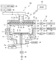
以下、本発明の実施の形態について図面を参照して詳細に説明する。図1は、本発明の実施の形態にかかるシリコン酸化膜の形成方法に利用可能なプラズマ処理装置100の概略構成を模式的に示す断面図である。また、図2は、図1のプラズマ処理装置100の平面アンテナを示す平面図である。
Hereinafter, embodiments of the present invention will be described in detail with reference to the drawings. FIG. 1 is a cross-sectional view schematically showing a schematic configuration of a
プラズマ処理装置100は、複数のスロット状の孔を有する平面アンテナ、特にRLSA(Radial Line Slot Antenna;ラジアルラインスロットアンテナ)にて直接処理室内にマイクロ波を導入して処理室内でプラズマを発生させることにより、高密度かつ低電子温度のマイクロ波励起プラズマを発生させ得るRLSAマイクロ波プラズマ処理装置として構成されている。プラズマ処理装置100では、1×10¹⁰〜5×10¹²/cm3のプラズマ密度で、かつ0.7〜2eVの低電子温度を有するプラズマによる処理が可能である。プラズマを生成する方式としては、誘導結合型方式(ICP,Induction Couplet Plasma)、マグネトロン方式、ECR方式(Electron cyclotron Resonance)、表面波方式で生成したプラズマも適用される。従って、プラズマ処理装置100は、各種半導体装置の製造過程において、シリコン酸化膜(例えばSiO2膜)を形成する目的で好適に利用できる。
The
プラズマ処理装置100は、主要な構成として、気密に構成されたチャンバー(処理室)1と、チャンバー1内にガスを供給するガス供給部としてのガス供給機構18と、チャンバー1内を減圧排気するための排気機構としての排気装置24と、チャンバー1の上部に設けられ、チャンバー1内にマイクロ波を導入するマイクロ波導入機構27と、これらプラズマ処理装置100の各構成部を制御する制御部50と、を備えている。
The
チャンバー1は、接地された略円筒状の容器により形成されている。なお、チャンバー1は角筒形状の容器により形成してもよい。チャンバー1は、アルミニウム等の材質からなる底壁1aと側壁1bとを有している。
The
チャンバー1の内部は、被処理体であるシリコン基板(ウエハW)を水平に支持するための載置台2が設けられている。載置台2は、熱伝導性の高い材質例えばAlN等のセラミックスにより構成されている。この載置台2は、排気室11の底部中央から上方に延びる円筒状の支持部材3により支持されている。支持部材3は、例えばAlN等のセラミックスにより構成されている。
Inside the
また、載置台2には、その外縁部をカバーし、ウエハWをガイドし、載置台2を覆うためのカバーリング4が設けられている。このカバーリング4は、環状に形成されていてもよく、載置台2の全面をカバーしていることが好ましい。カバーリング4によって、ウエハWへの不純物の混入防止を図ることができる。カバーリング4は、例えば石英、単結晶シリコン、ポリシリコン、アモルファスシリコン、SiN等の材質で構成され、これらの中でも石英がもっとも好ましい。また、カバーリング4を構成する前記材質は、アルカリ金属、金属などの不純物の含有量が少ない高純度のものが好ましい。
Further, the mounting table 2 is provided with a
また、載置台2には、温度調節機構としての抵抗加熱型のヒータ5が埋め込まれている。このヒータ5は、ヒータ電源5aから給電されることにより載置台2を加熱して、その熱で被処理体であるウエハWを均一に加熱する。
In addition, a resistance
また、載置台2には、熱電対(TC)6が配備されている。この熱電対6によって温度計測を行うことにより、ウエハWの加熱温度を例えば室温から900℃までの範囲で制御可能となっている。
The mounting table 2 is provided with a thermocouple (TC) 6. By measuring the temperature with the
また、載置台2には、ウエハWを支持して昇降させるためのウエハ支持ピン(図示せず)が設けられている。各ウエハ支持ピンは、載置台2の表面に対して突没可能に設けられている。 The mounting table 2 is provided with wafer support pins (not shown) for supporting the wafer W and raising and lowering it. Each wafer support pin is provided so as to protrude and retract with respect to the surface of the mounting table 2.
チャンバー1の内周には、石英からなる円筒状のライナー7が設けられている。また、載置台2の外周側には、チャンバー1内を均一排気するため、多数の排気孔8aを有する石英製のバッフルプレート8が環状に設けられている。このバッフルプレート8は、複数の支柱9により支持されている。
A
チャンバー1の底壁1aの略中央部には、円形の開口部10が形成されている。底壁1aにはこの開口部10と連通し、下方に向けて突出する排気室11が設けられている。この排気室11には、排気管12が接続されており、この排気管12を介して排気装置24に接続されている。
A
チャンバー1の上部には、環状のアッパープレート13が接合されている。アッパープレート13の内周は、内側(チャンバー内空間)へ向けて突出し、環状の支持部13aを形成している。
An annular
チャンバー1の側壁1bには、環状をなすガス導入部15が設けられている。このガス導入部15は、酸素含有ガスやプラズマ励起用ガスを供給するガス供給機構18に接続されている。なお、ガス導入部15はノズル状またはシャワー状に設けてもよい。
An annular
また、チャンバー1の側壁1bには、プラズマ処理装置100と、これに隣接する搬送室(図示せず)との間で、ウエハWの搬入出を行うための搬入出口16と、この搬入出口16を開閉するゲートバルブ17とが設けられている。
Further, on the
ガス供給機構18は、例えば不活性ガス供給源19aおよび酸素含有ガス供給源19bおよび水素ガス供給源19cを有している。なお、ガス供給機構18は、上記以外の図示しないガス供給源として、例えばチャンバー1内雰囲気を置換する際に用いるパージガス供給源、チャンバー1内をクリーニングする際に用いるクリーニングガス供給源等を有していてもよい。
The
不活性ガスはプラズマ励起用ガスとして使われ、安定したプラズマを生成することができ、例えば希ガスなどを用いることができる。希ガスとしては、例えばArガス、Krガス、Xeガス、Heガスなどを用いることができる。これらの中でも、経済性に優れている点でArガスを用いることが特に好ましい。また、酸素含有ガスとしては、例えば酸素ガス(O2)、水蒸気(H20)、一酸化窒素(NO)、一酸化二窒素(N20)などを用いることができる。 The inert gas is used as a plasma excitation gas and can generate a stable plasma. For example, a rare gas can be used. As the rare gas, for example, Ar gas, Kr gas, Xe gas, He gas, or the like can be used. Among these, it is particularly preferable to use Ar gas because it is economical. As the oxygen-containing gas, for example, oxygen gas (O 2 ), water vapor (H 2 0), nitrogen monoxide (NO), dinitrogen monoxide (N 2 0), or the like can be used.
不活性ガス、酸素含有ガスおよび水素ガスは、ガス供給機構18の不活性ガス供給源19a、酸素含有ガス供給源19bおよび水素ガス供給源から、ガスライン20を介してガス導入部15に至り、ガス導入部15からチャンバー1内に導入される。各ガス供給源に接続する各々のガスライン20には、マスフローコントローラ21およびその前後の開閉バルブ22が設けられている。このようなガス供給機構18の構成により、供給されるガスの切替えや流量等の制御が出来るようになっている。
The inert gas, the oxygen-containing gas, and the hydrogen gas reach the
排気機構としての排気装置24は、例えばターボ分子ポンプなどの高速真空ポンプ等の真空ポンプを備えている。前記のように、真空ポンプ24は、排気管12を介してチャンバー1の排気室11に接続されている。チャンバー1内のガスは、排気室11の空間11a内へ均一に流れ、さらに空間11aから真空ポンプ24を作動させることにより、排気管12を介して外部へ排気される。これにより、チャンバー1内を所定の真空度、例えば0.133Paまで高速に減圧することが可能となっている。
The exhaust device 24 as an exhaust mechanism includes a vacuum pump such as a high-speed vacuum pump such as a turbo molecular pump. As described above, the vacuum pump 24 is connected to the
次に、マイクロ波導入機構27の構成について説明する。マイクロ波導入機構27は、主要な構成として、透過板28、アンテナとしての平面アンテナ31、遅波材33、金属カバー34、導波管37、マッチング回路38およびマイクロ波発生装置39を備えている。
Next, the configuration of the
マイクロ波を透過させる透過板28は、アッパープレート13において内周側に突出した支持部13a上に配備されている。透過板28は、誘電体、例えば石英やA1203、AlN等のセラミックス等の部材で構成されている。この透過板28と支持部13aとの間は、Oリング等のシール部材29を介して気密にシールされている。したがって、チャンバー1内は気密に保持される。
The
アンテナとしての平面アンテナ31は、透過板28の上方(チャンバ1の外側)において、載置台2と対向するように設けられている。平面アンテナ31は、円板状をなしている。なお、平面アンテナ31の形状は、円板状に限らず、例えば四角板状でもよい。この平面アンテナ31は、アッパープレート13の上端に係止されている。
The
平面アンテナ31は、例えば表面が金または銀メッキされた銅板、アルミニウム板、ニッケル板およびそれらの合金などの導電性部材で構成されている。平面アンテナ31は、マイクロ波を放射する多数のスロット状のマイクロ波放射孔32を有している。マイクロ波放射孔32は、所定のパターンで平面アンテナ31を貫通して形成されている。
The
個々のマイクロ波放射孔32は、例えば図2に示すように、細長い長方形状(スロット状)をなしている。そして、典型的には隣接するマイクロ波放射孔32が「T」字状に配置されている。また、このように所定の形状(例えばT字状)に組み合わせて配置されたマイクロ波放射孔32は、さらに全体として同心円状に配置されている。 The individual microwave radiation holes 32 have an elongated rectangular shape (slot shape), for example, as shown in FIG. And typically, the adjacent microwave radiation holes 32 are arranged in a “T” shape. Further, the microwave radiation holes 32 arranged in combination in a predetermined shape (for example, T shape) are further arranged concentrically as a whole.
マイクロ波放射孔32の長さや配列間隔は、マイクロ波の波長(λg)に応じて決定される。例えば、マイクロ波放射孔32の間隔は、λg/4、λg/2またはλgとなるように配置される。なお、図2においては、同心円状に形成された隣接するマイクロ波放射孔32どうしの間隔を△rで示している。なお、マイクロ波放射孔32の形状は、円形状、円弧状等の他の形状であってもよい。さらに、マイクロ波放射孔32の配置形態は特に限定されず、同心円状のほか、例えば、螺旋状、放射状等に配置することもできる。
The length and arrangement interval of the microwave radiation holes 32 are determined according to the wavelength (λg) of the microwave. For example, the interval between the microwave radiation holes 32 is arranged to be λg / 4, λg / 2, or λg. In FIG. 2, the interval between adjacent microwave radiation holes 32 formed concentrically is indicated by Δr. Note that the
平面アンテナ31の上面には、真空よりも大きい誘電率を有する遅波材33が設けられている。この遅波材33は、真空中ではマイクロ波の波長が長くなることから、マイクロ波の波長を短くしてプラズマを調整する機能を有している。遅波材の材質としては、例えば石英、ポリテトラフルオロエチレン樹脂、ポリイミド樹脂などを用いることができる。
A
なお、平面アンテナ31と透過板28との間、また、遅波材33と平面アンテナ31との間は、それぞれ接触させても離間させてもよいが、接触させることが好ましい。
The
チャンバー1の上部には、これら平面アンテナ31および遅波材33を覆うように、金属カバー34が設けられている。金属カバー34は、例えばアルミニウムやステンレス鋼等の金属材料によって形成されている。金属カバー34と平面アンテナ31によって、偏平導波路が形成され、マイクロ波をチャンバー1内に均一に供給できるようになっている。アッパープレート13の上端と金属カバー34とは、シール部材35によりシールされている。また、金属カバー34の内部には、冷却水流路34aが形成されている。この冷却水流路34aに冷却水を通流させることにより、金属カバー34、遅波材33、平面アンテナ31および透過板28を冷却できるようになっている。なお、金属カバー34は接地されている。
A
金属カバー34の上壁(天井部)の中央には、開口部36が形成されており、この開口部36には導波管37が接続されている。導波管37の他端側には、マッチング回路38を介してマイクロ波を発生するマイクロ波発生装置39が接続されている。
An
導波管37は、上記金属カバー34の開口部36から上方へ延出する断面円形状の同軸導波管37aと、この同軸導波管37aの上端部にモード変換器40を介して接続された水平方向に延びる矩形導波管37bとを有している。モード変換器40は、矩形導波管37b内をTEモードで伝播するマイクロ波をTEMモードに変換する機能を有している。
The
同軸導波管37aの中心には内導体41が延在している。この内導体41は、その下端部において平面アンテナ31の中心に接続固定されている。このような構造により、マイクロ波は、同軸導波管37aの内導体41を介して平面アンテナ31により形成される偏平導波路へ放射状に効率よく均一に伝播される。
An
また、載置台2の表面側には電極42が埋設されている。この電極42にマッチングボックス(M.B.)43を介してバイアス印加用の高周波電源44が接続されており、電極42に高周波バイアス電力を供給することにより、ウエハW(被処理体)にバイアスを印加できる構成となっている。電極42の材質としては、例えばモリブデン、タングステンなどの導電性材料を用いることができる。電極42は、例えば網目状、格子状、渦巻き状等の形状に形成されている。
An
以上のような構成のマイクロ波導入機構27により、マイクロ波発生装置39で発生したマイクロ波が導波管37を介して平面アンテナ31へ伝搬され、さらにマイクロ波放射孔32(スロット)から透過板28を介してチャンバー1内に導入されるようになっている。なお、マイクロ波の周波数としては、例えば2.45GHzが好ましく用いられ、他に8.35GHz、1.98GHz等を用いることもできる。
With the
プラズマ処理装置100の各構成部は、制御部50に接続されて制御される構成となっている。制御部50は、典型的にはコンピュータであり、例えば図3に示したように、CPUを備えたプロセスコントローラ51と、このプロセスコントローラ51に接続されたユーザーインターフェース52および記憶部53を備えている。プロセスコントローラ51は、プラズマ処理装置100において、例えば温度、圧力、ガス流量、マイクロ波出力、バイアス印加用の高周波出力などのプロセス条件に関係する各構成部(例えば、ヒータ電源5a、ガス供給機構18、排気装置24、マイクロ波発生装置39、高周波電源44など)を統括して制御する制御手段である。
Each component of the
ユーザーインターフェース52は、工程管理者がプラズマ処理装置100を管理するためにコマンドの入力操作等を行うキーボードや、プラズマ処理装置100の稼働状況を可視化して表示するディスプレイ等を有している。また、記憶部53には、プラズマ処理装置100で実行される各種処理をプロセスコントローラ51の制御にて実現するための制御プログラム(ソフトウエア)や処理条件データ等が記録されたレシピなどが保存されている。
The
そして、必要に応じて、ユーザーインターフェース52からの指示等にて任意のレシピを記憶部53から呼び出してプロセスコントローラ51に実行させることで、プロセスコントローラ51により制御されてプラズマ処理装置100のチャンバー1内で所望の処理が行われる。また、前記制御プログラムや処理条件データ等のレシピは、コンピュータ読み取り可能な記憶媒体、例えばCD−ROM、ハードディスク、フレキシブルディスク、フラッシュメモリ、DVD、ブルーレイディスクなどに格納された状態のものを利用できる。さらに、前記レシピを他の装置から例えば専用回線を介して伝送させて利用することも可能である。
Then, if necessary, an arbitrary recipe is called from the
このように構成されたプラズマ処理装置100では、600℃以下例えば室温(25℃程度)以上600℃以下の低温で、被処理体上に形成された下地膜や基板(ウエハW)等へのダメージフリーなプラズマ処理を行うことができる。また、プラズマ処理装置100は、プラズマの均一性に優れていることから、大口径のウエハW(被処理体)に対してもプロセスの均一性を実現できる。
In the
次に、RLSA方式のプラズマ処理装置100を用いたプラズマ酸化処理について説明する。まず、ゲートバルブ17を開にして搬入出口16からウエハWをチャンバー1内に搬入し、載置台2上に載置する。
Next, plasma oxidation processing using the RLSA type
次に、チャンバー1内を真空ポンプにより減圧排気しながら、ガス供給機構18の不活性ガス供給源19a、酸素含有ガス供給源19bおよび水素ガス供給源19cから、不活性ガス、酸素含有ガスおよび必要に応じて水素ガスを所定の流量でそれぞれガス導入部15を介してチャンバー1内に導入する。このようにして、チャンバー1内を所定の圧力に調節する。
Next, while evacuating the inside of the
次に、マイクロ波発生装置39で発生させた所定周波数例えば2.45GHzのマイクロ波を、マッチング回路38を介して導波管37に導く。導波管37に導かれたマイクロ波は、矩形導波管37bおよび同軸導波管37aを順次通過し、内導体41を介して平面アンテナ31に供給される。つまり、マイクロ波は、矩形導波管37b内ではTEモードで伝搬し、このTEモードのマイクロ波はモード変換器40でTEMモードに変換されて、同軸導波管37a内を平面アンテナ31に向けて伝搬されていく。そして、マイクロ波は、平面アンテナ31に貫通形成されたスロット状のマイクロ波放射孔32から誘電体としての透過板28を介してチャンバー1内におけるウエハWの上方空間に放射される。この際のマイクロ波出力は、例えば200mm径以上のウエハWを処理する場合には、パワー密度として0.255〜2.55W/cm2の範囲内から選択することができる。
Next, a microwave having a predetermined frequency, for example, 2.45 GHz, generated by the
平面アンテナ31から透過板28を経てチャンバー1に放射されたマイクロ波により、チャンバー1内で電磁界が形成され、不活性ガスおよび酸素含有ガスがそれぞれプラズマ化する。このマイクロ波励起プラズマは、マイクロ波が平面アンテナ31の多数のマイクロ波放射孔32から放射されることにより、略1×10¹⁰〜5×10¹²/cm3の高密度で、かつウエハW近傍では、略1.2eV以下の低電子温度プラズマとなる。このようにして形成されるプラズマは、基板(ウエハW)へのイオン等によるプラズマダメージが少ない。その結果、プラズマ中の活性種例えばラジカルやイオンの作用によりウエハW表面に形成されたシリコン(単結晶シリコン、多結晶シリコンまたはアモルファスシリコン)に対してプラズマ酸化処理が行われ、ダメージのないシリコン酸化膜が形成される。
An electromagnetic field is formed in the
また、プラズマ酸化処理を行なっている間、載置台2に高周波電源44から所定の周波数およびパワーの高周波電力を供給する。この高周波電源44から供給される高周波電力によって、基板に高周波バイアス電圧(高周波バイアス)が印加され、その結果、プラズマの低い電子温度を維持しつつ、プラズマ酸化処理の異方性が促進される。すなわち、高周波バイアスが基板に印加されることにより、基板近傍に電磁界が形成され、これがプラズマ中のイオンを基板(ウエハW)へ引き込むように作用するため、シリコンの凹部や凸部の側壁へのイオンによる酸化作用を弱め、これらの部位での酸化レートを抑制する一方で、凹部の底壁では酸化レートを増大させるように作用する。従って、シリコンの凹部や凸部の側壁では等方性の酸化が抑制されて横方向に酸化膜が形成されにくくなり、凹凸パターンの寸法精度を維持できる。それに対して、凹部の底部では、高周波バイアスによってイオンが引き込まれ、十分な膜厚でシリコン酸化膜を形成することができる。
Further, high-frequency power having a predetermined frequency and power is supplied from the high-
<プラズマ酸化処理条件>
ここで、プラズマ処理装置100において行なわれるプラズマ酸化処理の好ましい条件について説明を行う。処理ガスとしては、希ガスとしてArガスを、酸素含有ガスとしてO2ガスをそれぞれ使用することが好ましい。このとき、処理ガス中に含まれるO2ガスの流量比率(体積比率)は、プラズマ処理の異方性を高め、凹凸の側壁の酸化を抑制しつつ、凹部の底部の酸化を促進させる観点から、0.1%以上50%以下の範囲内が好ましく、0.5%以上25%以下の範囲内がより好ましく、0.5%以上10%以下の範囲内がさらに好ましく、0.5%以上1%以下の範囲内が望ましい。つまり、チャンバー内の酸素分圧を低くしてプラズマを生成することによって、凹凸の内部はさらに酸素(イオン)分圧が低くなるので、バイアス印加により、酸素イオンが底部に引き込まれ、側壁部への酸素イオンの作用が抑制されるからである。
<Plasma oxidation treatment conditions>
Here, preferable conditions for the plasma oxidation process performed in the
また、本実施の形態では、処理ガス中に水素を含めることも可能である。水素を添加することにより、プラズマ中にOHラジカルが生成するため、酸化レートを増加させることが可能である。水素を使用する場合、高い酸化レートを得るために、処理ガス全体に対して水素と酸素の合計の流量比率(体積比率)を、0.1%以上50%以下の範囲内とすることが好ましく、0.5%以上25%以下の範囲内とすることがより好ましく、0.5%以上10%以下の範囲内とすることがさらに好ましく、0.5%以上1%以下の範囲内とすることが望ましい。この場合、水素と酸素の合計流量に対する水素流量の体積比率([H2流量/(H2+O2の合計流量)]×100)を1%以上90%以下の範囲内に設定することが好ましく、凹部の底部の酸化レートを向上させる観点からは10%以上60%以下の範囲内がより好ましく、特に凹凸部の側壁に形成されるシリコン酸化膜を凹部の底部に形成されるシリコン酸化膜よりも選択的に薄く形成する観点からは1%以上50%以下の範囲内とすることが望ましい。 In this embodiment mode, hydrogen can also be included in the processing gas. By adding hydrogen, OH radicals are generated in the plasma, so that the oxidation rate can be increased. When using hydrogen, in order to obtain a high oxidation rate, it is preferable that the total flow rate ratio (volume ratio) of hydrogen and oxygen with respect to the entire processing gas is within a range of 0.1% to 50%. More preferably in the range of 0.5% to 25%, still more preferably in the range of 0.5% to 10%, and in the range of 0.5% to 1%. It is desirable. In this case, it is preferable to set the volume ratio of the hydrogen flow rate to the total flow rate of hydrogen and oxygen ([H 2 flow rate / (total flow rate of H 2 + O 2 )] × 100) within a range of 1% to 90%. From the viewpoint of improving the oxidation rate at the bottom of the recess, the range of 10% to 60% is more preferable. In particular, the silicon oxide film formed on the side wall of the concavo-convex portion is more preferable than the silicon oxide film formed on the bottom of the recess. Also, from the viewpoint of selectively forming a thin film, it is desirable that the content be in the range of 1% to 50%.
また、処理圧力は、プラズマ酸化処理の異方性を高め、凹凸の側壁の酸化を抑制しつつ、凹部の底部の酸化を促進させる観点から、1.3Pa以上667Pa以下の範囲内に設定することが好ましく、6.7Pa以上133Pa以下の範囲内がより好ましく、20Pa以上60Pa以下の範囲内が望ましい。 In addition, the processing pressure is set within a range of 1.3 Pa or more and 667 Pa or less from the viewpoint of promoting the oxidation of the bottom of the concave portion while increasing the anisotropy of the plasma oxidation treatment and suppressing the oxidation of the side walls of the concave and convex portions. Is preferable, the range of 6.7 Pa to 133 Pa is more preferable, and the range of 20 Pa to 60 Pa is desirable.
また、上記処理ガス中の酸素流量比率と処理圧力の好ましい組み合わせは以下のとおりである。凹凸形状の側壁面のシリコン酸化膜の膜厚と、凹部の底壁面のシリコン酸化膜の膜厚との比[側壁面の膜厚/底壁面の膜厚]を0.01以上0.6以下とする場合には、処理ガス中の酸素の割合を0.5%以上50%以下の範囲内とし、かつ処理圧力を6.7Pa以上133Pa以下の範囲内とすることが好ましい。 Moreover, the preferable combination of the oxygen flow rate ratio in the said process gas and process pressure is as follows. The ratio of the thickness of the silicon oxide film on the concavo-convex sidewall surface to the thickness of the silicon oxide film on the bottom wall surface of the recess [side wall thickness / bottom wall thickness] is 0.01 or more and 0.6 or less In this case, it is preferable that the ratio of oxygen in the processing gas is in the range of 0.5% to 50% and the processing pressure is in the range of 6.7 Pa to 133 Pa.
また、凹凸形状の側壁面のシリコン酸化膜の膜厚と、凹部の底壁面のシリコン酸化膜の膜厚との比[側壁面の膜厚/底壁面の膜厚]を0.01以上0.4以下とする場合には、処理ガス中の酸素の割合を0.5%以上25%以下の範囲内とし、かつ処理圧力を20Pa以上60Pa以下の範囲内とすることが好ましい。 Further, the ratio of the thickness of the silicon oxide film on the concavo-convex side wall surface to the thickness of the silicon oxide film on the bottom wall surface of the recess [side wall surface thickness / bottom wall thickness] is 0.01 or more. In the case of 4 or less, it is preferable that the ratio of oxygen in the processing gas is in the range of 0.5% to 25% and the processing pressure is in the range of 20 Pa to 60 Pa.
本実施の形態では、プラズマ酸化処理を行なっている間、高周波電源44から所定の周波数およびパワーの高周波電力を載置台2に供給し、基板(ウエハW)に高周波バイアスを印加する。高周波電源44から供給される高周波電力の周波数は、例えば100kHz以上60MHz以下の範囲内が好ましく、400kHz以上13.5MHz以下の範囲内がより好ましい。高周波電力は、ウエハWの面積当たりのパワー密度として例えば0.2W/cm2以上2.3W/cm2以下の範囲内で印加することが好ましく、0.35W/cm2以上1.2W/cm2以下の範囲内で印加することがより好ましい。また、高周波のパワーは200W以上2000W以下の範囲内が好ましく、300W以上1200W以下の範囲内がより好ましい。載置台2に印加された高周波電力は、プラズマの低い電子温度を維持しつつ、プラズマ中のイオン種をウエハWへ引き込む作用を有している。従って、高周波電力を印加することにより、プラズマ酸化の異方性を高め、凹凸部の側壁部分に比べて底壁部分に形成されるシリコン酸化膜の膜厚を極端に大きくすることができる。また、本実施の形態では、ウエハWへ高周波バイアスを印加しても、低電子温度のプラズマであるため、シリコン酸化膜へのプラズマ中のイオン等によるダメージがなく、低温かつ短時間で良質なシリコン酸化膜を形成することが出来る。
In the present embodiment, high-frequency power having a predetermined frequency and power is supplied from the high-
また、プラズマ酸化処理におけるマイクロ波のパワー密度は、ラジカル成分を減らし、異方性を向上させる観点から、0.255W/cm2以上2.55W/cm2以下の範囲内とすることが好ましい。なお、本発明においてマイクロ波のパワー密度は、ウエハWの面積1cm2あたりのマイクロ波パワーを意味する。例えば300mm径以上のウエハWを処理する場合には、マイクロ波パワーを500W以上5000W未満の範囲内とすることが好ましく、1000W以上3000W以下とすることがより好ましい。 The power density of the microwave in the plasma oxidation process reduces the radical component, from the viewpoint of improving the anisotropy, it is preferable to 0.255W / cm 2 or more 2.55 W / cm 2 within the following ranges. In the present invention, the microwave power density means the microwave power per 1 cm 2 area of the wafer W. For example, when processing a wafer W having a diameter of 300 mm or more, the microwave power is preferably in the range of 500 W or more and less than 5000 W, and more preferably 1000 W or more and 3000 W or less.
また、ウエハWの加熱温度は、載置台2の温度として、例えば室温(25℃程度)以上600℃以下の範囲内とすることが好ましく、200℃以上500℃以下の範囲内に設定することがより好ましく、400℃以上500℃以下の範囲内に設定することが望ましい。 In addition, the heating temperature of the wafer W is preferably set in the range of room temperature (about 25 ° C.) to 600 ° C. as the temperature of the mounting table 2, and set in the range of 200 ° C. to 500 ° C. More preferably, it is desirable to set within the range of 400 ° C. or more and 500 ° C. or less.
以上の条件は、制御部50の記憶部53にレシピとして保存されている。そして、プロセスコントローラ51がそのレシピを読み出してプラズマ処理装置100の各構成部例えばガス供給機構18、排気装置24、マイクロ波発生装置39、ヒータ電源5a、高周波電源44などへ制御信号を送出することにより、所望の条件でのプラズマ酸化処理が実現する。
The above conditions are stored as a recipe in the
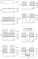
次に、図4(a)〜図4(i)を参照しながら、本発明のシリコン酸化膜の形成方法によりSTIにおけるトレンチ内表面にシリコン酸化膜を形成する場合を例に挙げて説明する。図4(a)〜図4(i)は、STIにおけるトレンチの形成とその後で行なわれる酸化膜形成までの工程を図示したものである。 Next, with reference to FIGS. 4A to 4I, a case where a silicon oxide film is formed on the inner surface of a trench in STI by the silicon oxide film forming method of the present invention will be described as an example. FIG. 4A to FIG. 4I illustrate the steps from formation of a trench in STI to subsequent oxide film formation.
まず、図4(a)および図4(b)において、シリコン基板101に例えば熱酸化などの方法によりSiO2などのシリコン酸化膜102を形成する。次に、図4(c)では、シリコン酸化膜102上に、例えばCVD(Chemical Vapor Deposition)によりSi3N4などのシリコン窒化膜103を形成する。さらに、図4(d)では、シリコン窒化膜103の上に、フォトレジストを塗布した後、フォトリソグラフィー技術によりパターニングしてレジスト層104を形成する。
First, in FIGS. 4A and 4B, a
次に、レジスト層104をエッチングマスクとし、例えばハロゲン系のエッチングガスを用いてシリコン窒化膜103とシリコン酸化膜102を選択的にプラズマエッチングする。このようにして、レジスト層104のパターンに対応してシリコン基板101を露出させる(図4(e))。また、シリコン窒化膜103により、トレンチのためのマスクパターンが形成される。図4(f)は、例えば酸素などを含む処理ガスを用いた酸素含有プラズマにより、いわゆるアッシング処理を実施し、レジスト層104を除去した状態を示している。
Next, using the resist
図4(g)では、シリコン窒化膜103およびシリコン酸化膜102をマスクとして、シリコン基板101に対し異方性プラズマエッチングを実施して、トレンチ105を形成する。このエッチングは、例えばCl2、HBr、SF6、CF4などのハロゲンまたはハロゲン化合物や、前記ハロゲン化合物にO2を含むエッチングガスを使用して行なうことができる。
In FIG. 4G, anisotropic plasma etching is performed on the
図4(h)は、STIにおけるエッチング後のウエハWのトレンチ105に対し、シリコン酸化膜を形成する工程を示している。ここでは、載置台2の電極42に上記範囲の周波数およびパワー(パワー密度)で高周波電力を供給しながら、処理ガス中の酸素の割合が0.1%以上50%以下の範囲内で、かつ処理圧力が1.3Pa以上667Pa以下の範囲内の条件でプラズマ酸化処理を行う。このような条件でプラズマ酸化処理を行なうことにより、図4(i)に示したように、トレンチ105の内表面を酸化してシリコン酸化膜111を形成することができる。このように選択的な酸化処理によって形成されたシリコン酸化膜111は、トレンチ105の側壁に形成されたシリコン酸化膜111aの膜厚と、トレンチ105の底部に形成されたシリコン酸化膜111bの膜厚との比[シリコン酸化膜111aの膜厚/シリコン酸化膜111bの膜厚]が、0.6以下例えば0.01から0.6の範囲内(好ましくは、0.01から0.4の範囲内)であり、トレンチ105の側壁部分のシリコン酸化膜111aの厚みを極端に抑えることができる。この場合、ゲート電極を形成する際にゲート長を減少させずに済み、デバイスのより微細化が実現される。
FIG. 4H shows a step of forming a silicon oxide film in the
STIにおける素子分離膜を埋めこむためのトレンチ105の側壁のシリコン酸化膜111aがシリコン基板101内で横方向に(側壁部分を)厚膜化すると、その分デバイス形成領域(例えば、DRAMであればメモリセル形成領域)の面積が縮小させられてしまう。例えば、トレンチ105の側壁に形成されたシリコン酸化膜111aの膜厚と、トレンチ105の底部に形成されたシリコン酸化膜111bの膜厚との比[シリコン酸化膜111aの膜厚/シリコン酸化膜111bの膜厚]が0.6を超えると、寸法精度に誤差が生じて微細化への対応が困難になる。従って、デバイス形成領域の面積を十分に確保しつつ微細化を図るためには、トレンチ105の側壁に形成されるシリコン酸化膜111aの膜厚を選択的に極力薄くすることが必要になる。本実施の形態では、トレンチ105の内面の酸化処理において、底部と側壁の酸化の選択性を高くして、側壁に形成されるシリコン酸化膜111aを底部のシリコン酸化膜111bに比べて極端に薄く形成することにより、デバイスの微細化への対応を図ることが可能になる。
When the
なお、本実施の形態のシリコン酸化膜の形成方法によってシリコン酸化膜111を形成した後は、STIによる素子分離領域形成の手順に従い、例えばCVD法によりトレンチ105内にSiO2などの絶縁膜を埋込んだ後、シリコン窒化膜103をストッパー層としてCMP(Chemical Mechanical Polishing)によって研磨を行ない平坦化する。平坦化した後は、エッチングまたはCMPによってシリコン窒化膜103および埋込み絶縁膜の上部を除去することにより、素子分離構造が形成される。
After the
また、本実施の形態のシリコン酸化膜の形成方法は、トランジスタのゲートエッチング後に行われるエッチングダメージ修復のための酸化処理にも適用可能である。例えば、図5(a)は、トランジスタのゲート電極となるポリシリコン電極200に対し、プラズマ酸化処理を施している状態を示している。シリコン基板101上にSiO2等の絶縁膜202を介してポリシリコン層を形成し、このポリシリコン層をレジスト等のエッチングマスク201を利用してライン&スペースのパターン形状にプラズマエッチングすることにより、ポリシリコン電極200が形成される。このプラズマエッチングの際に、ポリシリコン電極200の側面および基板表面にプラズマダメージが入る。この例では、ポリシリコン電極200が形成されたシリコン基板101に、図1のプラズマ処理装置100を用いてプラズマ酸化処理を行うことにより、エッチングによるプラズマダメージを修復するようにしている。プラズマ酸化処理は、載置台2に上記範囲の周波数およびパワー(パワー密度)で高周波電力を供給しながら、処理ガス中の酸素の割合が50%以下例えば0.1%以上50%以下の範囲内で、かつ処理圧力が667Pa以下例えば1.3Pa以上667Pa以下の範囲内の条件で行う。なお、プラズマ酸化処理により、図5(b)に示すように、ポリシリコン電極200の側面に薄いシリコン酸化膜203が形成される。
The method for forming a silicon oxide film of this embodiment can also be applied to an oxidation process for repairing etching damage performed after gate etching of a transistor. For example, FIG. 5A shows a state in which a plasma oxidation process is performed on a
トランジスタ設計上、ゲート電極となるポリシリコン電極200の側壁部分のシリコン酸化膜203が横方向(側壁部分)に厚膜化すると、その分ポリシリコン電極200内でトランジスタ形成部分の面積(チャンネル幅)が縮小してエッチングにより形成されたライン&スペースの寸法との間に誤差が生じてしまう。例えば、ポリシリコン電極200の側壁に形成されたシリコン酸化膜203の膜厚が厚くなると、上記誤差が大きくなり過ぎて、微細化への対応が困難になる。したがって、トランジスタ形成部分の面積を確保するためには、ポリシリコン電極200の側壁部分のシリコン酸化膜203の厚みを極端に薄く抑制する必要がある。本実施の形態のシリコン酸化膜の形成方法では、シリコン基板101とポリシリコン電極200の側壁との酸化処理の選択性を高め、側壁に形成されるシリコン酸化膜203を薄くすることにより寸法精度を維持し、微細化を図る上でもトランジスタ形成部分の面積を十分に確保することができるようになる。
In the transistor design, when the
また、プラズマ処理装置100を用いて、凹凸形状を有するシリコン表面に対してプラズマ酸化処理を行なう場合、主として載置台2へ供給する高周波電力、処理圧力および処理ガス中の酸素比率を調節することにより、凹部の底部と側壁との酸化処理の選択性を制御できる。例えば、図6(a)に示したように、処理圧力を高くするとプラズマ中のラジカルが増加するため酸化の等方性が強くなり、逆に、処理圧力を低くするとプラズマ中のイオンが増加するため酸化の異方性が強まる。また、図6(b)に示したように、処理ガス中のO2ガスの比率を増加させるとプラズマ中のイオンが減少するために酸化の等方性が強くなり、O2ガスの比率を低くするとプラズマ中のイオンが増加するために酸化の異方性が強まる。さらに、図6(c)に示したように、載置台2に供給する高周波電力が小さいと酸化の等方性が強くなり、高周波電力を大きくするに従い、プラズマ中のイオンがウエハWへ引き込まれやすくなるために酸化の異方性が極端に強くなる。
Further, when plasma oxidation processing is performed on a silicon surface having an uneven shape using the
本実施の形態のシリコン酸化膜の形成方法では、載置台2に高周波電力を供給して基板(ウエハW)に高周波バイアスを印加し、プラズマ中のイオンを基板(ウエハW)に引き込むことによって酸化の異方性を極端に高めるとともに、処理圧力を667Pa以下に設定し、かつ処理ガス中のO2比率を50%以下に設定した。このような条件設定により、酸化活性種としてイオン主体の酸化を行い、凹凸形状の底部と側壁とに形成されるシリコン酸化膜の厚みを選択的に制御している。 In the silicon oxide film forming method of the present embodiment, high-frequency power is supplied to the mounting table 2 to apply a high-frequency bias to the substrate (wafer W), and the ions in the plasma are drawn into the substrate (wafer W). The processing pressure was set to 667 Pa or lower, and the O 2 ratio in the processing gas was set to 50% or lower. Under such a condition setting, oxidation mainly of ions is performed as the oxidation active species, and the thickness of the silicon oxide film formed on the bottom and side walls of the concavo-convex shape is selectively controlled.
次に、本発明の効果を確認した試験結果について説明する。本実施の形態のシリコン酸化膜の形成方法を、凹凸形状(ライン&スペース)のパターンが形成されたシリコン表面の酸化膜形成に適用した。図7は、凹凸形状のパターン120を有するシリコン基板101のシリコン表面を酸化してシリコン酸化膜121を形成した後のウエハWの表面付近の断面構造を模式的に示したものである。本試験では、図1のプラズマ処理装置100を用い、下記の条件でシリコン表面に対してプラズマ酸化処理を行ない、シリコン酸化膜121を形成した。その後、TEM写真を撮影し、その画像から、凹凸形状のパターン120における凸部のトップの膜厚a、凹部の側壁の膜厚bおよび底部の膜厚cを測定し、各部の酸化レートと側壁/底部膜厚比(b/c)を算出した。なお、パターン120における凹部の開口幅L1は130nmであり、この開口幅L1と凹部の深さL2との比(アスペクト比L2/L1)は5であった。
Next, test results for confirming the effects of the present invention will be described. The method for forming a silicon oxide film according to the present embodiment was applied to the formation of an oxide film on a silicon surface on which a concavo-convex pattern (line and space) was formed. FIG. 7 schematically shows a cross-sectional structure near the surface of the wafer W after the silicon surface of the
これらの結果を表1から表3および図8から図14に示した。側壁/底部膜厚比(b/c)は、側壁と底部との酸化の選択性の指標であり、この値が小さいほど選択性が良好である。デバイスの微細化に対応するために、側壁のシリコン酸化膜の膜厚bは極力薄く形成することが好ましいからである。側壁/底部膜厚比(b/c)は、例えば0.6以下が好ましく、0.4以下がより好ましい。 These results are shown in Tables 1 to 3 and FIGS. The side wall / bottom film thickness ratio (b / c) is an index of the selectivity of oxidation between the side wall and the bottom, and the smaller the value, the better the selectivity. This is because it is preferable to form the silicon oxide film b on the side wall as thin as possible in order to cope with the miniaturization of the device. The side wall / bottom film thickness ratio (b / c) is preferably, for example, 0.6 or less, and more preferably 0.4 or less.
<実施例1〜4の共通条件>
高周波バイアスの周波数:13.56MHz
高周波バイアスのパワー:600W(パワー密度0.702W/cm2)
マイクロ波パワー:1200W(パワー密度0.614W/cm2)
処理温度:465℃
目標膜厚:6nm(トップ膜厚aとして)
ウエハ径:300mm
<比較例1の条件>
高周波バイアスを印加しない点以外は、実施例1〜4と同じである。
<Common conditions of Examples 1-4>
High frequency bias frequency: 13.56 MHz
High frequency bias power: 600 W (power density 0.702 W / cm 2 )
Microwave power: 1200 W (power density 0.614 W / cm 2 )
Processing temperature: 465 ° C
Target film thickness: 6 nm (as top film thickness a)
Wafer diameter: 300 mm
<Conditions of Comparative Example 1>
Except for not applying a high frequency bias, it is the same as Examples 1-4.

表1から、プラズマ酸化処理における側壁と底部の選択性の指標である側壁/底部膜厚比b/cに関しては、載置台2に高周波バイアスを印加せずにプラズマ酸化処理を行った比較例1では、側壁の膜厚が底部の膜厚より厚くなっており、その膜厚比b/cは、1.272となっており、略等方的に酸化が進行したことを示している。これに対して、載置台2に高周波電力を供給しながら、40Paから133Paの範囲内の比較的低い圧力条件でプラズマ酸化処理を行った実施例1〜実施例4では、側壁/底部膜厚比b/cが0.235〜0.376の範囲内であり、良好な結果を示した。これらの結果から、プラズマ酸化処理における側壁と底部の選択性を高め側壁の膜厚を薄くするには、載置台2に高周波バイアス電力を印加しながら133Pa以下例えば6.7Pa以上133Pa以下の比較的低い圧力条件を選択することが有効であり、しかも圧力を低くするほど側壁/底部膜厚比b/cを小さくでき側壁の膜厚を薄くできることが判明した。このことは、O2比率が1%と同じである実施例2と実施例4における膜厚比b/cの比較からも裏付けられた。 From Table 1, as for the side wall / bottom film thickness ratio b / c, which is an index of the selectivity between the side wall and the bottom in the plasma oxidation process, Comparative Example 1 in which the plasma oxidation process was performed without applying a high frequency bias to the mounting table 2. Then, the film thickness of the side wall is thicker than the film thickness of the bottom part, and the film thickness ratio b / c is 1.272, indicating that the oxidation has progressed substantially isotropically. On the other hand, in Example 1 to Example 4 in which plasma oxidation was performed under relatively low pressure conditions in the range of 40 Pa to 133 Pa while supplying high-frequency power to the mounting table 2, the sidewall / bottom film thickness ratio b / c was in the range of 0.235 to 0.376, and good results were shown. From these results, in order to increase the selectivity between the side wall and the bottom in the plasma oxidation process and to reduce the film thickness of the side wall, while applying high frequency bias power to the mounting table 2, it is relatively low at 133 Pa or less, for example, 6.7 Pa or more and 133 Pa or less. It has been found that it is effective to select a low pressure condition, and that the side wall / bottom film thickness ratio b / c can be reduced and the side wall film thickness can be reduced as the pressure is lowered. This was supported by a comparison of the film thickness ratio b / c between Example 2 and Example 4 where the O 2 ratio was the same as 1%.
また、処理圧力が同じ40Paである実施例1〜実施例3の比較から、O2比率が低いほど側壁/底部膜厚比b/cを低く抑制できることが示された。すなわち、O2比率が0.5%から1%の範囲内の実施例1および実施例2では、側壁/底部膜厚比b/cが0.235〜0.276の範囲内であり、O2比率が25%の実施例3(側壁/底部膜厚比b/c=0.376)に比べて側壁の膜厚を薄くできるという優れた結果を示した。これは、溝内の酸素イオン、ラジカルの分圧が低くなることで、側壁への酸化作用が抑制されることによるものである。 Further, from the comparison of the processing pressure is the same 40Pa Examples 1 3, O 2 ratio that can lower the suppressed lower side wall / bottom film thickness ratio b / c was shown. That is, in Example 1 and Example 2 in which the O 2 ratio is in the range of 0.5% to 1%, the side wall / bottom film thickness ratio b / c is in the range of 0.235 to 0.276. 2 ratio showed superior results that can reduce the film thickness of the sidewall as compared to the 25% of example 3 (side wall / bottom film thickness ratio b / c = 0.376). This is due to the fact that the partial pressure of oxygen ions and radicals in the groove is reduced, so that the oxidizing action on the side walls is suppressed.
図8は、実施例1から実施例3におけるプラズマ酸化処理での側壁と底部の膜厚比b/cと処理ガス中の酸素ガスの割合との関係をグラフ化したものである。この図8から、処理圧力が40Paの条件で、処理ガス中の酸素ガスの体積比率を50%以下にすれば、側壁/底部膜厚比b/cを0.6以下にすることが可能であり、同体積比率を25%以下にすれば側壁/底部膜厚比b/cを0.4以下にできることが判明した。 FIG. 8 is a graph showing the relationship between the film thickness ratio b / c between the side wall and the bottom in the plasma oxidation process in Examples 1 to 3 and the ratio of oxygen gas in the process gas. From FIG. 8, it is possible to reduce the side wall / bottom film thickness ratio b / c to 0.6 or less by setting the volume ratio of oxygen gas in the processing gas to 50% or less under the condition where the processing pressure is 40 Pa. It was found that the side wall / bottom film thickness ratio b / c can be reduced to 0.4 or less by setting the volume ratio to 25% or less.
図9は、実施例2〜4におけるプラズマ酸化処理での側壁と底部の膜厚比b/cと処理圧力との関係をグラフ化したものである。この図9から、1%O2の条件で、処理圧力267Pa以下にすれば、側壁/底部膜厚比b/cを0.6以下にすることが可能であり、処理圧力を133Pa以下にすれば、側壁/底部膜厚比b/cを0.4以下にでき側壁の膜厚を薄くできることが判明した。 FIG. 9 is a graph showing the relationship between the film thickness ratio b / c between the side wall and the bottom in the plasma oxidation process in Examples 2 to 4 and the processing pressure. From FIG. 9, when the processing pressure is 267 Pa or less under the condition of 1% O 2 , the side wall / bottom film thickness ratio b / c can be 0.6 or less, and the processing pressure is reduced to 133 Pa or less. Thus, it has been found that the side wall / bottom film thickness ratio b / c can be reduced to 0.4 or less, and the side wall film thickness can be reduced.
図10のグラフは、実施例1〜4および比較例1におけるシリコン酸化膜の側壁/底部膜厚比b/cと処理ガス中の酸素分圧との関係をプロットしたものである。この図10より、側壁/底部膜厚比b/cが0.4以下の、薄い膜厚の側壁にするためには処理ガス中の酸素分圧を10以下とすることが好ましく、2以下とすることがより好ましいことがわかる。 The graph of FIG. 10 plots the relationship between the side wall / bottom thickness ratio b / c of the silicon oxide film in Examples 1 to 4 and Comparative Example 1 and the oxygen partial pressure in the processing gas. From FIG. 10, it is preferable to set the oxygen partial pressure in the processing gas to 10 or less in order to obtain a thin film thickness side wall having a side wall / bottom film thickness ratio b / c of 0.4 or less. It turns out that it is more preferable to do.
図11は、実施例1におけるプラズマ酸化処理時間と、トップ膜厚aの平均膜厚および該平均膜厚のウエハ面内均一性との関係を示している。この図11に示されるように、実施例1の条件でプラズマ酸化処理を行った場合には、約180秒で目標膜厚(トップ膜厚a=6nm)に達しており、十分な酸化レートが得られている。また、プラズマ酸化処理におけるウエハ面内均一性は、4%以下で推移しており良好な結果であった。なお、図11におけるウエハ面内均一性は、(ウエハ面内の最大膜厚−同最小膜厚)/(ウエハ面内の平均膜厚×2)の百分率(×100%)により算出した(図12、図14も同様である)。 FIG. 11 shows the relationship between the plasma oxidation processing time in Example 1, the average film thickness of the top film thickness a, and the uniformity of the average film thickness within the wafer surface. As shown in FIG. 11, when the plasma oxidation process was performed under the conditions of Example 1, the target film thickness (top film thickness a = 6 nm) was reached in about 180 seconds, and a sufficient oxidation rate was obtained. Has been obtained. In addition, the wafer in-plane uniformity in the plasma oxidation treatment was 4% or less, which was a good result. In addition, the wafer in-plane uniformity in FIG. 11 was calculated by the percentage (× 100%) of (maximum film thickness in wafer surface−same minimum film thickness) / (average film thickness in wafer surface × 2) (FIG. 11). 12 and FIG. 14 are the same).
図12は、実施例2におけるプラズマ酸化処理時間と、トップ膜厚aの平均膜厚および該平均膜厚のウエハ面内均一性との関係を示している。この図12に示されるように、実施例1の条件でプラズマ酸化処理を行った場合には、約135秒で目標膜厚(トップ膜厚a=6nm)に達しており、十分な酸化レートが得られている。また、プラズマ酸化処理におけるウエハ面内均一性は、ほぼ2%以下で推移しており極めて良好な結果であった。 FIG. 12 shows the relationship between the plasma oxidation processing time in Example 2, the average film thickness of the top film thickness a, and the in-wafer uniformity of the average film thickness. As shown in FIG. 12, when the plasma oxidation process was performed under the conditions of Example 1, the target film thickness (top film thickness a = 6 nm) was reached in about 135 seconds, and a sufficient oxidation rate was obtained. Has been obtained. In addition, the in-plane uniformity of the wafer in the plasma oxidation treatment was almost 2% or less, which was a very good result.
図11および図12から、側壁/底部膜厚比b/cが0.4以下であった実施例1および実施例2のプラズマ酸化処理条件においても、実用上十分な酸化レートとウエハ面内均一性が得られることが確認された。 From FIG. 11 and FIG. 12, even in the plasma oxidation processing conditions of Example 1 and Example 2 where the side wall / bottom film thickness ratio b / c was 0.4 or less, a practically sufficient oxidation rate and uniform in-wafer surface were obtained. It was confirmed that the property was obtained.
次に、処理ガス中に水素を添加した実施例5〜8および比較例2、3の試験結果について、表2、表3、図13および図14を参照しながら説明する。 Next, test results of Examples 5 to 8 and Comparative Examples 2 and 3 in which hydrogen is added to the processing gas will be described with reference to Tables 2, 3 and 13 and FIG.
<実施例5〜8、比較例3の共通条件>
高周波バイアスの周波数:13.56MHz
マイクロ波パワー:1200W(パワー密度0.614W/cm2)
処理温度:465℃
目標膜厚:6nm(トップ膜厚aとして)
ウエハ径:300mm
<比較例2の条件>
高周波バイアスを印加しない点以外は、実施例5〜8、比較例3と同じである。
<Common conditions of Examples 5 to 8 and Comparative Example 3>
High frequency bias frequency: 13.56 MHz
Microwave power: 1200 W (power density 0.614 W / cm 2 )
Processing temperature: 465 ° C
Target film thickness: 6 nm (as top film thickness a)
Wafer diameter: 300 mm
<Conditions of Comparative Example 2>
Except not applying a high frequency bias, it is the same as Examples 5-8 and the comparative example 3. FIG.
表2および表3から、処理ガス中にH2を添加し、かつ載置台2に高周波バイアス電力を印加しながらプラズマ酸化処理を行うことによって、酸化レートを大幅に向上させ得ることが示された。水素の割合は0.1%以上2%未満が好ましく、0.1%〜1%がより好ましい。また、H2を添加しても、実施例5から8のように、載置台2に高周波バイアス電力を0.2[W/cm2]以上の電力密度で印加しながらプラズマ酸化処理を行うことによって、側壁と底部の選択性(つまり、側壁/底部膜厚比b/c)が実用上十分な値(側壁/底部膜厚比b/c=0.3〜0.6)であった。特に、40Paの処理圧力でプラズマ酸化処理を行った実施例8は、膜厚比b/c=0.3であり、高い酸化レートと側壁と底部の高い選択性とを両立でき、側壁の膜厚を薄くすることが出来た。このように、処理ガス中にH2を添加することにより、酸化レートを高め、スループットを向上させ得ることが判明した。 From Table 2 and Table 3, it was shown that the oxidation rate can be significantly improved by performing plasma oxidation treatment while adding H 2 to the processing gas and applying high-frequency bias power to the mounting table 2. . The proportion of hydrogen is preferably 0.1% or more and less than 2%, and more preferably 0.1% to 1%. Even if H 2 is added, plasma oxidation treatment is performed while applying high-frequency bias power to the mounting table 2 at a power density of 0.2 [W / cm 2 ] or more, as in Examples 5 to 8. Therefore, the selectivity between the side wall and the bottom (that is, the side wall / bottom film thickness ratio b / c) was a practically sufficient value (side wall / bottom film thickness ratio b / c = 0.3 to 0.6). In particular, Example 8 in which the plasma oxidation treatment was performed at a treatment pressure of 40 Pa had a film thickness ratio b / c = 0.3, and can achieve both a high oxidation rate and a high selectivity at the side wall and the bottom, and the film on the side wall. We were able to reduce the thickness. Thus, it has been found that by adding H 2 to the processing gas, the oxidation rate can be increased and the throughput can be improved.
また、実施例5から実施例8および比較例2、3におけるシリコン酸化膜の側壁/底部膜厚比b/cと高周波バイアスの電力密度(バイアスパワー)との関係を図13に示した。表2および図13より、処理圧力が667Paのときは、被処理体に印加する高周波バイアスの電力密度を0.2[W/cm2]以上とすることによって、側壁/底部膜厚比b/cを0.6以下にでき、側壁の膜厚を薄くできることが判明した。また、処理圧力が40Paのときは、被処理体に印加する高周波バイアスの電力密度を0.2[W/cm2]以上とすることによって側壁/底部膜厚比b/cを0.6以下にすることが可能であり、さらに高周波バイアスの電力密度を0.35[W/cm2]以上とすることによって、側壁/底部膜厚比b/cを0.4以下にでき、側壁の膜厚を薄く出来ることが判明した。 FIG. 13 shows the relationship between the silicon oxide film sidewall / bottom film thickness ratio b / c and the power density (bias power) of the high frequency bias in Examples 5 to 8 and Comparative Examples 2 and 3. From Table 2 and FIG. 13, when the processing pressure is 667 Pa, the side wall / bottom film thickness ratio b / is set by setting the power density of the high frequency bias applied to the object to be processed to 0.2 [W / cm 2 ] or more. It was found that c can be made 0.6 or less, and the thickness of the sidewall can be reduced. When the processing pressure is 40 Pa, the sidewall / bottom film thickness ratio b / c is 0.6 or less by setting the power density of the high frequency bias applied to the object to be processed to 0.2 [W / cm 2 ] or more. Further, by setting the power density of the high frequency bias to 0.35 [W / cm 2 ] or more, the side wall / bottom film thickness ratio b / c can be made 0.4 or less, and the film on the side wall It has been found that the thickness can be reduced.
一方、処理ガス中に水素を添加した場合でも、被処理体(ウエハW)に高周波バイアスを印加しなかった比較例2や、高周波バイアスの電力密度が0.16[W/cm2]と小さかった比較例3では、十分な酸化レートが得られず、しかも膜厚比b/cが0.8〜1.2と選択性が低い結果となった。従って、プラズマ酸化処理における側壁と底部の高い選択性を得ながら、側壁の膜厚を薄くし、酸化レートを大きくしたい場合には、載置台2に高周波バイアス電力を供給しながら、処理ガス中にH2を添加することが好ましいことが判明した。 On the other hand, even when hydrogen is added to the processing gas, Comparative Example 2 in which no high frequency bias is applied to the object to be processed (wafer W), and the power density of the high frequency bias is as small as 0.16 [W / cm 2 ]. In Comparative Example 3, a sufficient oxidation rate was not obtained, and the film thickness ratio b / c was 0.8 to 1.2, resulting in low selectivity. Therefore, in the case where it is desired to reduce the thickness of the sidewall and increase the oxidation rate while obtaining high selectivity between the sidewall and the bottom in the plasma oxidation process, the high-frequency bias power is supplied to the mounting table 2 in the processing gas. It has been found preferable to add H 2 .
図14は、実施例8におけるプラズマ酸化処理時間と、トップ膜厚aの平均膜厚および該平均膜厚のウエハ面内均一性との関係を示している。この図14に示されるように、実施例8の条件でプラズマ酸化処理を行った場合には、約90秒で目標膜厚(トップ膜厚a=6nm)に達しており、非常に大きな酸化レートが得られている。このように、処理ガス中にH2を添加することにより、7.1nm/minという大きな酸化レートを実現することができ、側壁の膜厚を薄く維持しつつスループットを向上させ得ることが確認できた。 FIG. 14 shows the relationship between the plasma oxidation processing time in Example 8, the average film thickness of the top film thickness a, and the in-wafer uniformity of the average film thickness. As shown in FIG. 14, when the plasma oxidation process was performed under the conditions of Example 8, the target film thickness (top film thickness a = 6 nm) was reached in about 90 seconds, and a very large oxidation rate was achieved. Is obtained. Thus, by adding H 2 to the processing gas, a large oxidation rate of 7.1 nm / min can be realized, and it can be confirmed that the throughput can be improved while the film thickness of the sidewall is kept thin. It was.
以上詳述したように、プラズマ処理装置100を使用し、凹凸パターンを有するウエハWの表面に露出したシリコン部分に処理ガスのプラズマによる酸化処理を施してシリコン酸化膜を形成する場合に、処理ガス中の酸素の割合を0.1%以上50%以下の範囲内とし、かつ処理圧力を1.3Pa以上667Pa以下の範囲内とすることにより、側壁/底部膜厚比b/cを0.6以下例えば0.01以上0.6以下の範囲内にすることができる。従って、例えばSTIにおけるトレンチ内の酸化処理や、トランジスタのゲートエッチング後のエッチングダメージ修復のための酸化などにおいて、側壁部分の酸化膜厚を極力薄くしながら、底部に必要な膜厚でシリコン酸化膜を選択的に形成することができる。その結果、凹凸パターンの横方向の寸法精度が確保され、デバイスの微細設計への対応が可能になる。
As described above in detail, when the
また、処理ガス中にH2を添加することにより、酸化レートを高くして短時間に凹凸形状の凹部の底壁面に20nm以下例えば6nm以上20nm以下の範囲内の膜厚でかつ、側壁には0.6nm以上12nm以下の膜厚でシリコン酸化膜を薄く形成することができる。 Further, by adding H 2 to the processing gas, the oxidation rate is increased, and the thickness of the bottom wall surface of the concave-convex recess is 20 nm or less, for example, in the range of 6 nm or more and 20 nm or less, and the side wall is formed on the side wall. A silicon oxide film can be thinly formed with a thickness of 0.6 nm to 12 nm.
以上、本発明の実施の形態を挙げて説明したが、本発明は上記実施の形態に限定されることなく、種々の変形が可能である。例えば上記実施の形態では、本発明のシリコン酸化膜の形成方法を行う装置として最適なRLSA方式のプラズマ処理装置を例に挙げて説明した。しかし、例えばICPプラズマ方式、ECRプラズマ方式、表面反射波プラズマ方式、マグネトロンプラズマ方式等の他のプラズマ処理装置を使用することも可能である。 As described above, the embodiments of the present invention have been described. However, the present invention is not limited to the above embodiments, and various modifications can be made. For example, in the above-described embodiment, the RLSA type plasma processing apparatus that is optimal as an apparatus for performing the silicon oxide film forming method of the present invention has been described as an example. However, other plasma processing apparatuses such as an ICP plasma system, an ECR plasma system, a surface reflection wave plasma system, and a magnetron plasma system can be used.
また、上記実施の形態では、凹凸パターンに対するシリコン酸化膜形成の例として、STIにおける単結晶のシリコン基板101のトレンチ105内部の酸化処理、およびエッチングによってトランジスタのポリシリコンゲート電極を形成した後のエッチングダメージ修復のための酸化処理について説明した。しかし、本発明のシリコン酸化膜の形成方法は、凹凸パターンの表面にシリコン酸化膜を形成する必要性の高い他の種々のアプリケーションにも適用できる。さらに、凹凸によって部位により面方位が相違するシリコン表面例えばフィン構造や溝ゲート構造などの3次元トランジスタの製造過程で、ゲート絶縁膜等としてのシリコン酸化膜を選択的に側壁に薄く形成する場合にも適用可能である。また、逆に凹凸シリコンの底部に選択的に厚くシリコン酸化膜を形成したい場合にも適用できる。
Further, in the above embodiment, as an example of forming a silicon oxide film for the concavo-convex pattern, etching after forming the polysilicon gate electrode of the transistor by oxidation inside the
図15および図16に、本発明に係るシリコン酸化膜の形成方法を、フラッシュメモリを製造する工程に適用した事例を示す。図15(a)に示すように、まず、シリコン基板301上に、基板を熱酸化処理してSiO2の第1の絶縁膜層302を形成し、その上にCVDにより第1のポリシリコン層303、Si3N4層およびSiO2層で構成される第2の絶縁膜層304を積層形成し、さらにその上に第2のポリシリコン層305を形成する。周知のように、フラッシュメモリデバイスでは、第1の絶縁層302はトンネル酸化膜として作動し、第1のポリシリコン層303はフローティングゲートとして作動し、第2のポリシリコン層305はコントロールゲートとして作動する。これらの層をシリコン基板301上に形成する方法についても、周知である。
15 and 16 show an example in which the method for forming a silicon oxide film according to the present invention is applied to a process for manufacturing a flash memory. As shown in FIG. 15A, first, a substrate is thermally oxidized on a
図15(a)には示していないが、次に、第2のポリシリコン層305上にフォトレジストを塗布し、これをフォトリソグラフィー技術によってパターニングしてエッチングのためのマスク306とする。その後、このようにして形成されたマスク306を利用して、例えばプラズマエッチングを行うことによって、図15(b)に示すように、シリコン基板301にトレンチ307を一気に形成し、各メモリ領域を分離する。
Although not shown in FIG. 15A, next, a photoresist is applied on the
次に、図16(a)に示すように、トレンチ307に対して本発明の方法に従ってプラズマ酸化処理を行い、トレンチ307の内表面にシリコン酸化膜308を形成する。このようにすることによって、トレンチ307の側壁におけるシリコン酸化膜308aの膜厚を底部のシリコン酸化膜308bの膜厚に比べて極端に薄く形成することができるため、本デバイスでは、個々のメモリ素子においてゲート長を長く取ることができる。
Next, as shown in FIG. 16A, plasma oxidation is performed on the
次に、図16(b)に示すように、マスク306を例えばアッシングによって除去し、適宜メタル配線(図示せず)を形成した後、例えばCVDまたはプラズマCVDによりSiO2などの層間絶縁膜309を形成して、各メモリ領域を埋め込み、フラッシュメモリを完成する。上述したように、このフラッシュメモリでは、各メモリ素子の側壁に形成されるシリコン酸化膜の膜厚を非常に薄くすることが可能なため、素子を微細化しつつゲート長を長く取ることができる。これによって、メモリ容量が大きくかつ動作の信頼性が高いフラッシュメモリを得ることができる。
Next, as shown in FIG. 16B, the
1…チャンバー(処理室)、2…載置台、3…支持部材、5…ヒ一夕、12…排気管、15…ガス導入部、16…搬入出口、17…ゲートバルブ、18…ガス供給機構、19a…不活性ガス供給源、19b…酸素含有ガス供給源、19c…水素ガス供給源、24…排気装置、28…透過板、29…シール部材、31…平面アンテナ、32…マイクロ波放射孔、37…導波管、37a…同軸導波管、37b…矩形導波管、39…マイクロ波発生装置、50…制御部、51…プロセスコントローラ、52…ユーザーインターフェース、53…記憶部、100…プラズマ処理装置、101…シリコン基板、102…シリコン酸化膜、103…シリコン窒化膜、105…トレンチ、120…パターン、121…シリコン酸化膜、200…ポリシリコン電極、W…半導体ウエハ(基板)
DESCRIPTION OF
Claims (11)
前記処理室内で被処理体を載置する載置台に被処理体の面積当り0.2W/cm2以上2.3W/cm2以下の範囲内の出力で高周波電力を印加しながら、前記処理ガス中の酸素の割合が体積比で0.1%以上50%以下の範囲内であり、処理圧力が1.3Pa以上667Pa以下の範囲内の条件で前記プラズマを生成させることにより、前記凹凸形状の側壁面に形成される前記シリコン酸化膜の膜厚と、凹部の底壁面に形成される前記シリコン酸化膜の膜厚との比[側壁面の膜厚/底壁面の膜厚]を0.6以下とすることを特徴とするシリコン酸化膜の形成方法。 In this method, a silicon oxide film is formed by forming a silicon oxide film by applying a plasma of a processing gas to a silicon portion exposed on the surface of an object to be processed having an uneven shape in a processing chamber of a plasma processing apparatus. And
While applying the high frequency power at the output of the area per 0.2 W / cm 2 or more 2.3 W / cm 2 or less in the range of the object on the mounting table mounting the object to be processed in the processing chamber, the processing gas By generating the plasma under the condition that the ratio of oxygen in the volume ratio is 0.1% or more and 50% or less and the processing pressure is 1.3 Pa or more and 667 Pa or less, The ratio of the thickness of the silicon oxide film formed on the side wall surface to the thickness of the silicon oxide film formed on the bottom wall surface of the recess [side wall surface thickness / bottom wall thickness] is 0.6. A method for forming a silicon oxide film, comprising:
前記制御プログラムは、実行時に、プラズマ処理装置の処理室内で、凹凸形状を有する被処理体の表面に露出したシリコン部分に対し、被処理体を載置する載置台に被処理体の面積当り0.2W/cm2以上2.3W/cm2以下の範囲内の出力で高周波電力を印加しながら、処理ガス中の酸素の割合が体積比で0.1%以上50%以下の範囲内であり、かつ処理圧力が1.3Pa以上667Pa以下の範囲内である条件で生成させた処理ガスのプラズマを作用させることによって酸化処理を施し、前記凹凸形状の側壁面に形成される前記シリコン酸化膜の膜厚と、凹部の底壁面に形成される前記シリコン酸化膜の膜厚との比[側壁面の膜厚/底壁面の膜厚]が0.6以下になるようにシリコン酸化膜を形成するシリコン酸化膜の形成方法が行われるようにコンピュータに前記プラズマ処理装置を制御させるものであることを特徴とするコンピュータ読み取り可能な記憶媒体。 A computer-readable storage medium storing a control program that runs on a computer,
The control program executes 0 per area of the object to be processed on a mounting table on which the object to be processed is placed on a silicon portion exposed on the surface of the object to be processed having an uneven shape in the processing chamber of the plasma processing apparatus. while applying the high frequency power at the output of the .2W / cm 2 or more 2.3 W / cm 2 or less in the range, the proportion of oxygen in the process gas is in the range less than 50% greater than 0.1% by volume And an oxidation treatment is performed by applying plasma of a processing gas generated under a condition where a processing pressure is in a range of 1.3 Pa or more and 667 Pa or less, and the silicon oxide film formed on the uneven side wall surface is formed. The silicon oxide film is formed so that the ratio of the film thickness to the film thickness of the silicon oxide film formed on the bottom wall surface of the recess [side wall film thickness / bottom wall film thickness] is 0.6 or less. Silicon oxide film formation method A computer-readable storage medium characterized by causing a computer to control the plasma processing apparatus.
前記処理室の前記開口部を塞ぐ誘電体部材と、
前記誘電体部材の外側に設けられ、前記処理室内に電磁波を導入するためのアンテナと、
前記処理室内に原料ガスを供給するガス供給機構と、
前記処理室内を減圧排気する排気機構と、
前記処理室内で被処理体を載置する載置台と、
前記載置台に接続された高周波電源と、
前記処理室内で、凹凸形状を有する被処理体表面に露出したシリコン部分に処理ガスのプラズマによる酸化処理を施してシリコン酸化膜を形成するにあたり、
前記載置台に被処理体の面積当り0.2W/cm2以上2.3W/cm2以下の範囲内の出力で高周波電力を印加するとともに、前記ガス供給機構によって供給される前記処理ガス中の酸素の割合を体積比で0.1%以上50%以下の範囲内とし、かつ前記排気機構により処理圧力を1.3Pa以上667Pa以下の範囲内としながら、前記アンテナによって前記処理室内に電磁波を導入することにより前記プラズマを生成させて、前記凹凸形状の側壁面に形成される前記シリコン酸化膜の膜厚と、凹部の底壁面に形成される前記シリコン酸化膜の膜厚との比[側壁面の膜厚/底壁面の膜厚]が0.6以下となるように制御する制御部と、
を備えたことを特徴とするプラズマ処理装置。 A processing chamber having an open top for processing an object to be processed using plasma;
A dielectric member that closes the opening of the processing chamber;
An antenna provided outside the dielectric member for introducing electromagnetic waves into the processing chamber;
A gas supply mechanism for supplying a source gas into the processing chamber;
An exhaust mechanism for exhausting the processing chamber under reduced pressure;
A mounting table for mounting an object to be processed in the processing chamber;
A high-frequency power source connected to the mounting table;
In forming a silicon oxide film by subjecting the silicon portion exposed to the surface of the object to be processed having an uneven shape in the processing chamber to oxidation treatment with plasma of a processing gas.
Applies a high frequency power at the output in the range of 2.3 W / cm 2 or less per unit area of 0.2 W / cm 2 or more of the workpiece to the mounting table, in the process gas supplied by the gas supply mechanism Electromagnetic waves are introduced into the processing chamber by the antenna while the oxygen ratio is in the range of 0.1% to 50% by volume and the processing pressure is in the range of 1.3 Pa to 667 Pa by the exhaust mechanism. Ratio of the film thickness of the silicon oxide film formed on the concavo-convex shape side wall surface and the film thickness of the silicon oxide film formed on the bottom wall surface of the recess [side wall surface The film thickness / the thickness of the bottom wall surface] is controlled to be 0.6 or less,
A plasma processing apparatus comprising:
Priority Applications (1)
| Application Number | Priority Date | Filing Date | Title |
|---|---|---|---|
| JP2009013724A JP2009200483A (en) | 2008-01-24 | 2009-01-24 | Method for forming silicon oxide film |
Applications Claiming Priority (2)
| Application Number | Priority Date | Filing Date | Title |
|---|---|---|---|
| JP2008013564 | 2008-01-24 | ||
| JP2009013724A JP2009200483A (en) | 2008-01-24 | 2009-01-24 | Method for forming silicon oxide film |
Publications (2)
| Publication Number | Publication Date |
|---|---|
| JP2009200483A true JP2009200483A (en) | 2009-09-03 |
| JP2009200483A5 JP2009200483A5 (en) | 2012-01-26 |
Family
ID=40901251
Family Applications (1)
| Application Number | Title | Priority Date | Filing Date |
|---|---|---|---|
| JP2009013724A Pending JP2009200483A (en) | 2008-01-24 | 2009-01-24 | Method for forming silicon oxide film |
Country Status (5)
| Country | Link |
|---|---|
| US (1) | US20110017586A1 (en) |
| JP (1) | JP2009200483A (en) |
| KR (1) | KR101249611B1 (en) |
| TW (1) | TW200941579A (en) |
| WO (1) | WO2009093760A1 (en) |
Cited By (4)
| Publication number | Priority date | Publication date | Assignee | Title |
|---|---|---|---|---|
| JP2009239157A (en) * | 2008-03-28 | 2009-10-15 | Toshiba Corp | Method of manufacturing semiconductor device |
| WO2011040455A1 (en) * | 2009-09-30 | 2011-04-07 | 東京エレクトロン株式会社 | Selective plasma nitriding method and plasma nitriding device |
| JP2012216667A (en) * | 2011-03-31 | 2012-11-08 | Tokyo Electron Ltd | Plasma treatment method |
| WO2018179038A1 (en) * | 2017-03-27 | 2018-10-04 | 株式会社Kokusai Electric | Semiconductor device production method, program and substrate processing device |
Families Citing this family (7)
| Publication number | Priority date | Publication date | Assignee | Title |
|---|---|---|---|---|
| JP2011097029A (en) * | 2009-09-30 | 2011-05-12 | Tokyo Electron Ltd | Process for manufacturing semiconductor device |
| US8642479B2 (en) * | 2011-07-14 | 2014-02-04 | Nanya Technology Corporation | Method for forming openings in semiconductor device |
| WO2013047464A1 (en) | 2011-09-28 | 2013-04-04 | 東京エレクトロン株式会社 | Etching method and device |
| KR101854609B1 (en) | 2011-12-27 | 2018-05-08 | 삼성전자주식회사 | Method of Forming a Gate Insulating Layer |
| US20130320453A1 (en) * | 2012-06-01 | 2013-12-05 | Abhijit Jayant Pethe | Area scaling on trigate transistors |
| JP2014209515A (en) * | 2013-04-16 | 2014-11-06 | 東京エレクトロン株式会社 | Etching method |
| JP6125467B2 (en) * | 2014-06-16 | 2017-05-10 | 富士フイルム株式会社 | Print order receiving machine, its operating method and operating program |
Citations (7)
| Publication number | Priority date | Publication date | Assignee | Title |
|---|---|---|---|---|
| JP2002033381A (en) * | 2000-07-19 | 2002-01-31 | Mitsubishi Electric Corp | Formation method of element isolation insulating film and manufacturing method of semiconductor device |
| WO2002058130A1 (en) * | 2001-01-22 | 2002-07-25 | Tokyo Electron Limited | Method for producing material of electronic device |
| JP2002280369A (en) * | 2001-03-19 | 2002-09-27 | Canon Sales Co Inc | Apparatus and method of forming oxide film on silicon substrate |
| WO2004023549A1 (en) * | 2002-08-30 | 2004-03-18 | Fujitsu Amd Semiconductor Limited | Semiconductor device and its manufacturing method |
| JP2005286339A (en) * | 2004-03-29 | 2005-10-13 | Sharp Corp | High-density plasma process for producing silicon dioxide on silicon carbide substrate |
| JP2005294551A (en) * | 2004-03-31 | 2005-10-20 | Toshiba Corp | Method and apparatus for oxidation treatment of silicon based material, and manufacturing method for semiconductor device |
| WO2006073568A2 (en) * | 2004-11-16 | 2006-07-13 | Applied Materials, Inc. | MULTI-LAYER HIGH QUALITY GATE DIELECTRIC FOR LOW-TEMPERATURE POLY-SILICON TFTs |
Family Cites Families (6)
| Publication number | Priority date | Publication date | Assignee | Title |
|---|---|---|---|---|
| JPH0519296A (en) * | 1991-07-12 | 1993-01-29 | Matsushita Electric Ind Co Ltd | Method and device for forming insulating film |
| JPH11219950A (en) * | 1998-02-03 | 1999-08-10 | Hitachi Ltd | Manufacture of semiconductor integrated circuit and manufacturing device thereof |
| JP3505493B2 (en) * | 1999-09-16 | 2004-03-08 | 松下電器産業株式会社 | Method for manufacturing semiconductor device |
| JP2004047950A (en) * | 2002-04-03 | 2004-02-12 | Hitachi Kokusai Electric Inc | Method for manufacturing semiconductor and equipment for manufacturing semiconductor |
| JP4694108B2 (en) * | 2003-05-23 | 2011-06-08 | 東京エレクトロン株式会社 | Oxide film forming method, oxide film forming apparatus, and electronic device material |
| JP2006286662A (en) * | 2005-03-31 | 2006-10-19 | Toshiba Corp | Oxidation treatment method of silicon-based treatment object, oxidation treatment apparatus and method of manufacturing semiconductor apparatus |
-
2009
- 2009-01-23 KR KR1020107017810A patent/KR101249611B1/en active IP Right Grant
- 2009-01-23 TW TW098103133A patent/TW200941579A/en unknown
- 2009-01-23 WO PCT/JP2009/051517 patent/WO2009093760A1/en active Application Filing
- 2009-01-24 JP JP2009013724A patent/JP2009200483A/en active Pending
-
2010
- 2010-07-22 US US12/805,301 patent/US20110017586A1/en not_active Abandoned
Patent Citations (7)
| Publication number | Priority date | Publication date | Assignee | Title |
|---|---|---|---|---|
| JP2002033381A (en) * | 2000-07-19 | 2002-01-31 | Mitsubishi Electric Corp | Formation method of element isolation insulating film and manufacturing method of semiconductor device |
| WO2002058130A1 (en) * | 2001-01-22 | 2002-07-25 | Tokyo Electron Limited | Method for producing material of electronic device |
| JP2002280369A (en) * | 2001-03-19 | 2002-09-27 | Canon Sales Co Inc | Apparatus and method of forming oxide film on silicon substrate |
| WO2004023549A1 (en) * | 2002-08-30 | 2004-03-18 | Fujitsu Amd Semiconductor Limited | Semiconductor device and its manufacturing method |
| JP2005286339A (en) * | 2004-03-29 | 2005-10-13 | Sharp Corp | High-density plasma process for producing silicon dioxide on silicon carbide substrate |
| JP2005294551A (en) * | 2004-03-31 | 2005-10-20 | Toshiba Corp | Method and apparatus for oxidation treatment of silicon based material, and manufacturing method for semiconductor device |
| WO2006073568A2 (en) * | 2004-11-16 | 2006-07-13 | Applied Materials, Inc. | MULTI-LAYER HIGH QUALITY GATE DIELECTRIC FOR LOW-TEMPERATURE POLY-SILICON TFTs |
Cited By (10)
| Publication number | Priority date | Publication date | Assignee | Title |
|---|---|---|---|---|
| JP2009239157A (en) * | 2008-03-28 | 2009-10-15 | Toshiba Corp | Method of manufacturing semiconductor device |
| US7858467B2 (en) | 2008-03-28 | 2010-12-28 | Kabushiki Kaisha Toshiba | Method of manufacturing semiconductor device |
| US8097503B2 (en) | 2008-03-28 | 2012-01-17 | Kabushiki Kaisha Toshiba | Method of manufacturing semiconductor device |
| US8404537B2 (en) | 2008-03-28 | 2013-03-26 | Kabushiki Kaisha Toshiba | Method of manufacturing semiconductor device |
| WO2011040455A1 (en) * | 2009-09-30 | 2011-04-07 | 東京エレクトロン株式会社 | Selective plasma nitriding method and plasma nitriding device |
| JP2011077321A (en) * | 2009-09-30 | 2011-04-14 | Tokyo Electron Ltd | Selective plasma nitriding method, and plasma nitriding device |
| US20120184111A1 (en) * | 2009-09-30 | 2012-07-19 | Tokyo Electron Limited | Selective plasma nitriding method and plasma nitriding apparatus |
| JP2012216667A (en) * | 2011-03-31 | 2012-11-08 | Tokyo Electron Ltd | Plasma treatment method |
| WO2018179038A1 (en) * | 2017-03-27 | 2018-10-04 | 株式会社Kokusai Electric | Semiconductor device production method, program and substrate processing device |
| US10796900B2 (en) | 2017-03-27 | 2020-10-06 | Kokusai Electric Corporation | Method of manufacturing semiconductor device |
Also Published As
| Publication number | Publication date |
|---|---|
| US20110017586A1 (en) | 2011-01-27 |
| TW200941579A (en) | 2009-10-01 |
| KR101249611B1 (en) | 2013-04-01 |
| KR20100119547A (en) | 2010-11-09 |
| WO2009093760A1 (en) | 2009-07-30 |
Similar Documents
| Publication | Publication Date | Title |
|---|---|---|
| JP5073482B2 (en) | Silicon oxide film manufacturing method, control program thereof, storage medium, and plasma processing apparatus | |
| JP5138261B2 (en) | Silicon oxide film forming method, plasma processing apparatus, and storage medium | |
| KR101249611B1 (en) | Method for forming silicon oxide film, storage medium, and plasma processing apparatus | |
| TWI515791B (en) | Plasma etching method and plasma etching device | |
| JP5231233B2 (en) | Plasma oxidation processing method, plasma processing apparatus, and storage medium | |
| WO2011040426A1 (en) | Process for manufacturing semiconductor device | |
| JP5089121B2 (en) | Method for forming silicon oxide film and plasma processing apparatus | |
| JP4906659B2 (en) | Method for forming silicon oxide film | |
| JP2011077321A (en) | Selective plasma nitriding method, and plasma nitriding device | |
| JP5231232B2 (en) | Plasma oxidation processing method, plasma processing apparatus, and storage medium | |
| US8389420B2 (en) | Method and apparatus for forming silicon oxide film | |
| JP5271702B2 (en) | Silicon oxide film forming method and silicon oxide film forming apparatus |
Legal Events
| Date | Code | Title | Description |
|---|---|---|---|
| A521 | Request for written amendment filed |
Free format text: JAPANESE INTERMEDIATE CODE: A523 Effective date: 20111130 Free format text: JAPANESE INTERMEDIATE CODE: A821 Effective date: 20111130 |
|
| A621 | Written request for application examination |
Free format text: JAPANESE INTERMEDIATE CODE: A621 Effective date: 20111130 |
|
| A977 | Report on retrieval |
Free format text: JAPANESE INTERMEDIATE CODE: A971007 Effective date: 20120524 |
|
| A131 | Notification of reasons for refusal |
Free format text: JAPANESE INTERMEDIATE CODE: A131 Effective date: 20120529 |
|
| A02 | Decision of refusal |
Free format text: JAPANESE INTERMEDIATE CODE: A02 Effective date: 20130507 |