JP2009181804A - Transmission cable with shield - Google Patents
Transmission cable with shield Download PDFInfo
- Publication number
- JP2009181804A JP2009181804A JP2008019639A JP2008019639A JP2009181804A JP 2009181804 A JP2009181804 A JP 2009181804A JP 2008019639 A JP2008019639 A JP 2008019639A JP 2008019639 A JP2008019639 A JP 2008019639A JP 2009181804 A JP2009181804 A JP 2009181804A
- Authority
- JP
- Japan
- Prior art keywords
- conductor
- loss
- shield
- transmission line
- current
- Prior art date
- Legal status (The legal status is an assumption and is not a legal conclusion. Google has not performed a legal analysis and makes no representation as to the accuracy of the status listed.)
- Pending
Links
Images


Abstract
Description
本発明は、高周波成分を含む電気信号を伝送するためのシールド付き伝送線路、とくにシールド付きケーブルおよび多層プリント配線基板に関するものである。 The present invention relates to a transmission line with a shield for transmitting an electrical signal containing a high-frequency component, and more particularly to a shielded cable and a multilayer printed wiring board.
近年の半導体集積回路の処理速度向上に伴い、電子機器の内部や電子機器の間で、1GHz以上の高周波成分を含む高速な電気信号がやりとりされるようになった。その結果、ケーブルやプリント配線基板などの伝送線路の部分で意図せざる高周波電磁界が発生して、機器の誤動作や、人体・隣接電子機器に悪影響を与える可能性が懸念されている。このため、1GHz以上の高周波帯でも電磁ノイズの発生を規制する動きが広がっており、伝送線路部分での不要電磁界の発生を抑制する技術が必要になっている。 With the recent increase in processing speed of semiconductor integrated circuits, high-speed electrical signals including high-frequency components of 1 GHz or higher have been exchanged inside and between electronic devices. As a result, an unintended high-frequency electromagnetic field is generated in a transmission line portion such as a cable or a printed wiring board, and there is a concern that the device may malfunction or adversely affect human bodies or adjacent electronic devices. For this reason, the movement which regulates generation | occurrence | production of electromagnetic noise has spread also in the high frequency band of 1 GHz or more, and the technique which suppresses generation | occurrence | production of the unnecessary electromagnetic field in a transmission line part is needed.
伝送線路からの不要電磁界の発生を抑える技術としては、従来から、伝送線路の周囲にシールド層を設けて、伝送線路を流れる電流によって発生する電磁界をシールド層の内部または近傍に閉じ込める対策が実施されてきた。一般に、伝送線路は、往路電流と帰路電流が流れる少なくとも二本以上の導線から構成され、シールド層は多くの場合、導体材料によって構成される。以下では、上述の伝送線路を構成する二本以上の導線を、単に伝送線路を構成する導線と略記する。伝送線路の周囲にシールド層を設置する際の形態には、大別して次の二種類がある。 Conventionally, as a technique for suppressing the generation of unnecessary electromagnetic fields from transmission lines, there has been a measure to provide a shield layer around the transmission line and confine the electromagnetic field generated by the current flowing through the transmission line in or near the shield layer. Has been implemented. In general, a transmission line is composed of at least two conductors through which a forward current and a return current flow, and the shield layer is often composed of a conductor material. Hereinafter, two or more conductors constituting the above-described transmission line are simply abbreviated as conductors constituting the transmission line. There are roughly the following two types of forms when the shield layer is installed around the transmission line.
まず、第一のシールド層の設置形態においては、伝送線路を構成する導線の外側に、伝送線路を構成する導線とは別な導体から成るシールド層を追加する。これによって、伝送線路を構成する導線で発生する電磁界が、シールド層の近傍または内部に閉じ込められる。また、第二のシールド設置形態においては、シールド層として新たな導体を追加するのではなく、伝送線路を構成する導線のうちの一部の導線が、他の導線の一部または全部を覆う構造とする。これによって、上記の一部の導線がシールド層としての機能を持ち、他の導線で発生する電磁界が、上記の一部の導線の近傍または内部に閉じ込められる。 First, in the installation form of the first shield layer, a shield layer made of a conductor different from the conductor constituting the transmission line is added outside the conductor constituting the transmission line. As a result, the electromagnetic field generated by the conducting wire constituting the transmission line is confined in the vicinity of or inside the shield layer. Further, in the second shield installation form, instead of adding a new conductor as a shield layer, a structure in which a part of the conductors constituting the transmission line covers a part or all of the other conductors. And As a result, the above-mentioned part of the conductors has a function as a shield layer, and an electromagnetic field generated by the other conductors is confined in the vicinity of or inside the part of the conductors.
上述の第一のシールド層の設置形態の例としては、シールド付きペアケーブル(TwinAx)やシールド付きカッドケーブル、シールド付きツイストペアケーブル(FTP)、シールド付きフラットケーブル(FFC)、リジッドプリント配線基板またはフレキシブルプリント配線基板上のマイクロストリップ線路などがある。また、同じく上述の第二のシールド設置形態の例としては、同軸ケーブルや、リジッドプリント配線基板またはフレキシブルプリント配線基板上のストリップ線路などがある。ただし、以上の例は、あくまでも従来技術によるシールド付き伝送線路において、シールド層の設置形態の分類を明確にするために例示したものであって、本発明の適用範囲を限定するものではない。 Examples of the installation form of the first shield layer described above include shielded pair cable (TwinAx), shielded quad cable, shielded twisted pair cable (FTP), shielded flat cable (FFC), rigid printed wiring board, or flexible There is a microstrip line on a printed wiring board. Similarly, examples of the second shield installation form include a coaxial cable, a strip line on a rigid printed wiring board or a flexible printed wiring board, and the like. However, the above example is merely illustrated for clarifying the classification of the installation form of the shield layer in the shielded transmission line according to the prior art, and does not limit the application range of the present invention.
従来技術について記載した非特許文献1としては、「高速信号ボードの設計(応用編)」の(10.2 同軸ケーブルのノイズと干渉)がある。ここで非特許文献1として同軸ケーブルに関する文献を挙げたのは、同軸ケーブルは構造が単純なために、シールド層を流れる不要電流の分析が最も進んでいるからであり、本発明の適用範囲が同軸ケーブルに限定されることを意味するものではない。
また特開平9−129041号公報(特許文献1)には高周波用の伝送線路において、シールド層を導電率が異なる複数の導体で構成することが開示されている。 Japanese Patent Laid-Open No. 9-129041 (Patent Document 1) discloses that, in a high-frequency transmission line, the shield layer is composed of a plurality of conductors having different conductivities.
しかしながら従来の技術では、伝送線路自体から発生する電磁界をシールド層の近傍または内部に閉じ込めることは可能であるが、シールド層が導体によって構成されているために、シールド層を電子回路に接続すると、信号伝送の目的とは直接関係のない電流がシールド層に流れて、それが新たな不要電磁界の発生源になってしまうという問題があった。このために従来の技術では、シールド層に電流を流さないようにシールド層と電子回路の接続部にコモンモードチョークなどのノイズ対策部品を追加する対策がとられてきた。
またそのほかにも、上述の原因から考えて合理的な対策とは言いがたいが、シールド層を厚くしてシールド層の遮蔽性能を上げるという対策もとられてきた。
However, in the conventional technology, it is possible to confine the electromagnetic field generated from the transmission line itself in the vicinity or inside of the shield layer. However, since the shield layer is composed of a conductor, the shield layer is connected to an electronic circuit. However, there is a problem in that a current that is not directly related to the purpose of signal transmission flows through the shield layer, which becomes a new source of unnecessary electromagnetic fields. For this reason, in the prior art, measures have been taken to add a noise countermeasure component such as a common mode choke at the connection between the shield layer and the electronic circuit so that no current flows in the shield layer.
In addition to this, it is difficult to say that this is a reasonable measure in view of the above causes, but a measure has been taken to increase the shielding performance of the shield layer by increasing the thickness of the shield layer.
しかしこれらは、新たにノイズ対策部品を追加する方法や、シールド層の膜厚を厚くする方法であるためシールド付き伝送線路のコストが高くなるという問題があった。 However, these are a method of adding a new noise countermeasure component and a method of increasing the thickness of the shield layer, and thus there is a problem that the cost of the shielded transmission line is increased.
また特許文献1記載の方法は、同軸ケーブルの外部から同軸ケーブルの内部への熱伝達を抑制するための方法であり、そのためにシールド層を99%以上の高損失材料で構成するものである。しかしながら、この構成では高周波領域において電磁ノイズの発生量を少なくすることはできないという問題があった。
The method described in
そこで本発明の目的は、上記課題を解決し、高周波領域において電磁ノイズの発生量が少なく、かつ良好な信号伝送特性を持つシールド付き伝送線路を、低コストに提供することにある。 SUMMARY OF THE INVENTION Accordingly, an object of the present invention is to solve the above problems and provide a shielded transmission line having a low amount of electromagnetic noise generated in a high frequency region and having good signal transmission characteristics at a low cost.
本発明では上記の課題を解決するために、請求項1の発明は伝送線路の入力側と出力側を電気的に接続するために設けられた一本以上の導体線と、伝送線路の入力側と出力側を電気的に接続するとともに前記導体線から発生する不要電磁界をシールドするための一本以上のシールド導体線と、前記導体線と前記シールド導体線を保持し互いに電気的に絶縁するための絶縁体によって構成されるシールド付き伝送線路において、前記シールド導体線を導電率が異なる二種類以上の導体材料によって構成し、かつ、前記シールド導体線の前記導体線に近い側に低損失導体材料、前記導体線から遠い側に高損失導体材料を配置したことを特徴とするシールド付き伝送線路である。
In order to solve the above-mentioned problems in the present invention, the invention of
請求項2の発明は、伝送線路の入力側と出力側を電気的に接続するために設けられた二本以上の導体線と、前記導体線を保持し互いに電気的に絶縁するための絶縁体と、前記導体線から発生する不要電磁界をシールドするためのシールド導体によって構成されるシールド付き伝送線路において、前記シールド導体を導電率が異なる二種類以上の導体材料によって構成し、かつ、前記シールド導体の前記導体線に近い側に低損失導体材料、前記導体線から遠い側に高損失導体材料を配置し、かつ、前記高損失導体材料の厚みを前記低損失材料の厚みよりも小さくしたことを特徴とするシールド付き伝送線路である。 According to a second aspect of the present invention, there are provided two or more conductor wires provided to electrically connect an input side and an output side of a transmission line, and an insulator for holding the conductor wires and electrically insulating each other. And a shielded transmission line constituted by a shield conductor for shielding an unnecessary electromagnetic field generated from the conductor wire, wherein the shield conductor is constituted by two or more kinds of conductor materials having different conductivity, and the shield A low-loss conductor material is disposed on the side of the conductor close to the conductor wire, a high-loss conductor material is disposed on the side far from the conductor wire, and the thickness of the high-loss conductor material is smaller than the thickness of the low-loss material. It is a transmission line with a shield characterized by these.
請求項3の発明は、伝送線路の入力側と出力側を電気的に接続するために設けられた一本以上の導体線と、伝送線路の入力側と出力側を電気的に接続するとともに前記導体線から発生する不要電磁界をシールドするための一本以上のシールド導体線と、前記導体線と前記シールド導体線を保持し互いに電気的に絶縁するための絶縁体によって構成されるシールド付き伝送線路において、前記シールド導体線を導電率が異なる二種類以上の導体材料によって構成し、かつ、前記シールド導体線の前記導体線に近い側に低損失導体材料、前記導体線から遠い側に高損失導体材料を配置し、かつ、前記高損失導体材料の厚みを前記低損失材料の厚みよりも小さくしたことを特徴とするシールド付き伝送線路である。 According to a third aspect of the present invention, the one or more conductor wires provided for electrically connecting the input side and the output side of the transmission line, the input side and the output side of the transmission line are electrically connected, and Shielded transmission comprising one or more shielded conductor wires for shielding unwanted electromagnetic fields generated from the conductor wires, and an insulator for holding the conductor wires and the shield conductor wires and electrically insulating them from each other In the line, the shield conductor wire is composed of two or more kinds of conductor materials having different electrical conductivities, and a low loss conductor material is provided on the side of the shield conductor wire close to the conductor wire, and a high loss is provided on the side far from the conductor wire. The shielded transmission line is characterized in that a conductor material is disposed and the thickness of the high loss conductor material is smaller than the thickness of the low loss material.
請求項4の発明は、伝送線路の入力側と出力側を電気的に接続するために設けられた二本以上の導体線と、前記導体線を保持し互いに電気的に絶縁するための絶縁体と、前記導体線から発生する不要電磁界をシールドするためのシールド導体によって構成されるシールド付き伝送線路において、前記シールド導体を導電率が異なる二種類以上の導体材料によって構成し、かつ、前記シールド導体の前記導体線に近い側に低損失導体材料、前記導体線から遠い側に高損失導体材料を配置し、かつ、前記高損失導体材料の厚みを前記低損失材料の厚みよりも小さくし、かつ、前記高損失導体材料の厚みを、前記シールド付き伝送線路からの不要電磁界の発生を抑制したい周波数領域の下限値νminにおける表皮深さδ(νmin)よりも大きくしたことを特徴とするシールド付き伝送線路である。 According to a fourth aspect of the present invention, there are provided two or more conductor wires provided for electrically connecting an input side and an output side of a transmission line, and an insulator for holding the conductor wires and electrically insulating each other. And a shielded transmission line constituted by a shield conductor for shielding an unnecessary electromagnetic field generated from the conductor wire, wherein the shield conductor is constituted by two or more kinds of conductor materials having different conductivity, and the shield A low loss conductor material on the side of the conductor close to the conductor wire, a high loss conductor material on the side far from the conductor wire, and the thickness of the high loss conductor material is smaller than the thickness of the low loss material; and that the thickness of the high losses conductive material, and larger than the skin depth at the lower limit value [nu min of the frequency region to suppress the generation of unnecessary electromagnetic field from the shielded transmission line δ (ν min) A shielded transmission line to the butterflies.
請求項5の発明は、伝送線路の入力側と出力側を電気的に接続するために設けられた一本以上の導体線と、伝送線路の入力側と出力側を電気的に接続するとともに前記導体線から発生する不要電磁界をシールドするための一本以上のシールド導体線と、前記導体線と前記シールド導体線を保持し互いに電気的に絶縁するための絶縁体によって構成されるシールド付き伝送線路において、前記シールド導体線を導電率が異なる二種類以上の導体材料によって構成し、かつ、前記シールド導体線の前記導体線に近い側に低損失導体材料、前記導体線から遠い側に高損失導体材料を配置し、かつ、前記高損失導体材料の厚みを前記低損失材料の厚みよりも小さくし、かつ、前記高損失導体材料の厚みを、前記シールド付き伝送線路からの不要電磁界の発生を抑制したい周波数領域の下限値νminにおける表皮深さδ(νmin)よりも大きくしたことを特徴とするシールド付き伝送線路である。 According to a fifth aspect of the present invention, the one or more conductor lines provided for electrically connecting the input side and the output side of the transmission line, the input side and the output side of the transmission line are electrically connected, and Shielded transmission comprising one or more shielded conductor wires for shielding unwanted electromagnetic fields generated from the conductor wires, and an insulator for holding the conductor wires and the shield conductor wires and electrically insulating them from each other In the line, the shield conductor wire is composed of two or more kinds of conductor materials having different electrical conductivities, and a low loss conductor material is provided on the side of the shield conductor wire close to the conductor wire, and a high loss is provided on the side far from the conductor wire. A conductive material is disposed, and the thickness of the high-loss conductor material is made smaller than the thickness of the low-loss material, and the thickness of the high-loss conductor material is reduced to an unnecessary electromagnetic field from the shielded transmission line. A shielded transmission line, characterized in that is larger than the skin depth δ (ν min) in the lower limit value [nu min of the frequency region to be suppressed from occurring.
請求項6の発明は、請求項4に記載のシールド導体をシールド層に使用したことを特徴とする、シールド付きペアケーブル、およびシールド付きツイストペアケーブルを含むシールド付き多線ケーブルである。 The invention of claim 6 is a shielded multi-wire cable including a shielded pair cable and a shielded twisted pair cable, wherein the shield conductor according to claim 4 is used for a shield layer.
請求項7の発明は、請求項5に記載のシールド導体線を外部導体として使用したことを特徴とする同軸ケーブルである。 A seventh aspect of the present invention is a coaxial cable characterized by using the shield conductor wire according to the fifth aspect as an outer conductor.
請求項8の発明は、請求項4に記載のシールド導体を、ストリップ線路のグランド配線として使用したことを特徴とするリジッドプリント基板およびフレキシブルプリント基板である。 The invention according to claim 8 is a rigid printed board and a flexible printed board characterized in that the shield conductor according to claim 4 is used as a ground wiring of a strip line.
請求項9の発明は、請求項5に記載のシールド導体線を、マイクロストリップ線路のグランド配線または電源配線として使用したことを特徴とするリジッドプリント基板およびフレキシブルプリント基板である。 A ninth aspect of the present invention is a rigid printed circuit board and a flexible printed circuit board characterized in that the shield conductor line according to the fifth aspect is used as a ground wiring or a power supply wiring of a microstrip line.
請求項10の発明は、請求項4に記載のシールド導体をシールド層に使用したことを特徴とするフレキシブルフラットケーブルである。 The invention of claim 10 is a flexible flat cable characterized in that the shield conductor according to claim 4 is used for a shield layer.
請求項11の発明は、外部導体を複数の導体線を撚り合わせた撚り線層によって構成したことを特徴とする同軸ケーブルにおいて、前記外部導体を二層以上の撚り線層によって構成し、かつ、前記撚り線層の内側の層を低損失導体材料、外側の層を高損失導体材料によって構成し、かつ、前記高損失導体材料によって構成した撚り線層の厚みを、前記低損失導体材料によって構成した撚り線層の厚みよりも小さくしたことを特徴とする同軸ケーブルである。
The invention according to
請求項12の発明は、外部導体を複数の導体線を撚り合わせた撚り線層によって構成したことを特徴とする同軸ケーブルにおいて、前記外部導体を二層以上の撚り線層によって構成し、かつ、前記撚り線層の内側の層を低損失導体材料、外側の層を高損失導体材料によって構成し、かつ、前記高損失導体材料によって構成した撚り線層の厚みを、前記低損失導体材料によって構成した撚り線層の厚みよりも小さくし、かつ、前記高損失導体材料によって構成した撚り線層の厚みを、前記同軸ケーブルからの不要電磁界の発生を抑制したい周波数領域の下限値νminにおける表皮深さδ(νmin)よりも大きくしたことを特徴とする同軸ケーブルである。
The invention according to
請求項13の発明は、内部導体を構成する一本の導体線と、外部導体を構成する一本の中空導体線と、内部導体と外部導体を保持し互いに電気的に絶縁するための絶縁体からなるセミリジッド同軸ケーブルにおいて、前記外部導体を二種類以上の導体材料によって構成し、かつ前記外部導体の内側表面に低損失導体材料、外側表面に高損失導体材料を配置し、かつ、前記高損失導体材料の厚みを前記低損失材料の厚みよりも小さくしたことを特徴とするセミリジッド同軸ケーブルである。
The invention according to
請求項14の発明は、内部導体を構成する一本の導体線と、外部導体を構成する一本の中空導体線と、内部導体と外部導体を保持し互いに電気的に絶縁するための絶縁体からなるセミリジッド同軸ケーブルにおいて、前記外部導体を二種類以上の導体材料によって構成し、かつ前記外部導体の内側表面に低損失導体材料、外側表面に高損失導体材料を配置し、かつ、前記高損失導体材料の厚みを前記低損失材料の厚みよりも小さくし、かつ、前記高損失導体材料の厚みを、前記セミリジッド同軸ケーブルからの不要電磁界の発生を抑制したい周波数領域の下限値νminにおける表皮深さδ(νmin)よりも大きくしたことを特徴とするセミリジッド同軸ケーブルである。
The invention according to
請求項15の発明は、請求項14に記載のセミリジッド同軸ケーブルにおいて、外部導体を、低損失導体材料からなる中空導体線の外側表面に高損失導体材料をメッキすることによって形成したことを特徴とするセミリジッド同軸ケーブルである。
The invention of claim 15 is the semi-rigid coaxial cable according to
本発明によれば、高周波領域において電磁ノイズの発生量が少なく、かつ良好な信号伝送特性を持つシールド付き伝送線路を、低コストで実現することができる。 According to the present invention, it is possible to realize a shielded transmission line that generates a small amount of electromagnetic noise in a high frequency region and has good signal transmission characteristics at a low cost.
まず本発明の原理について以下に詳述する。
本発明では、シールド導体を流れる不要電流の高周波成分がシールド導体表面の薄い表面層に集中し、かつ、上述の不要電流の高周波成分が、伝送線路から遠い側のシールド導体表面に集中して流れるという事実に着目した。すなわち、本発明は、上述の不要電流の高周波成分を減衰させるために、シールド導体の伝送線路から遠い側の表面に、高周波電流層の厚さ、すなわち表皮深さδ(ν)よりも厚い高損失導体層を設けたことを特徴としている。ここで、周波数νにおける表皮深さδ(ν)は、周知のように、導体材料の透磁率μと導電率σを用いて次の数式(1)によって与えられる。

In the present invention, the high-frequency component of the unnecessary current flowing through the shield conductor is concentrated on the thin surface layer of the shield conductor surface, and the above-described high-frequency component of the unnecessary current flows concentrated on the shield conductor surface far from the transmission line. Focused on the fact that. That is, in order to attenuate the high-frequency component of the above-described unnecessary current, the present invention provides a high-frequency current layer having a thickness higher than the skin depth δ (ν) on the surface far from the transmission line of the shield conductor. A lossy conductor layer is provided. Here, the skin depth δ (ν) at the frequency ν is given by the following equation (1) using the magnetic permeability μ and the conductivity σ of the conductor material, as is well known.
以下、図面を参照して本発明の作用を詳細に説明する。なお、全ての図において同一の機能を有するものには同一符号を付け、その繰り返しの説明は省略する。 Hereinafter, the operation of the present invention will be described in detail with reference to the drawings. Note that components having the same function are denoted by the same reference symbols throughout the drawings, and repeated description thereof is omitted.
まず、シールド層を持たない伝送線路からの不要電磁界の発生機構を図1に示す。一般に、電気信号を送信側回路1から受信側回路3に伝送するためには、伝送線路2を介して送信側回路1と受信側回路3を接続する必要がある。伝送線路2を構成する導線21は、送信側回路1の信号源11と受信側回路3の負荷31を接続し、その結果として、受信側回路3の負荷31を流れる電流または負荷31の両端に現れる電圧が受信信号として検出される。この際、導線21を流れる電流は電磁気学の法則にしたがって電磁界22を発生し、それが伝送線路の外部において不要電磁界として観測される。
First, FIG. 1 shows a mechanism for generating an unnecessary electromagnetic field from a transmission line having no shield layer. Generally, in order to transmit an electrical signal from the
次に、シールド付き伝送線路からの不要電磁界の発生機構を図2(a)に示す。一般に、シールド付き伝送線路のシールド層は、伝送線路を構成する導線21をシールド導体23によって部分的または完全に覆うことによって、導線21に流れる電流から発生する電磁界22を、シールド導体23の近傍または内部に閉じ込める役割を果たす。
Next, FIG. 2A shows a mechanism for generating an unnecessary electromagnetic field from the shielded transmission line. In general, the shield layer of a shielded transmission line is configured so that the
しかし、図2(b)にその一例を示す従来技術によるシールド付き伝送線路においては、シールド導体23を送信側回路1および受信側回路3に電気的に接続した際に、信号伝送とは直接関係がない不要電流25がシールド導体23を流れることができるため、シールド導体を設けることによって新たな不要電磁界26が発生してしまうという問題がある。
However, in the transmission line with a shield according to the prior art, an example of which is shown in FIG. 2B, when the
この際、高周波においては電流の流れる経路が導体表面の表皮深さδ(ν)の領域に限定されるという事実と、高周波電流はインピーダンスを最小にする経路を流れるという一般法則を用いると、上述の不要電磁界26は、シールド導体23の伝送線路から遠い側の表面を流れることが分かる。また、流れる不要電流25の大きさは、(i)送信側回路と受信側回路の設計、(ii)シールド導体と送信側回路および受信側回路の接続方法、(iii)シールド層の電気抵抗、が決まるとほぼ決まってしまうので、従来技術によるシールド付き伝送線路では、シールド上を流れる不要電流25による不要電磁界26の発生を抑制することは困難である。
At this time, when the fact that the current flow path is limited to the area of the skin depth δ (ν) of the conductor surface at high frequency and the general law that the high frequency current flows through the path that minimizes the impedance is used, It can be seen that the unnecessary
これに対して、図2(c)にその一例を示す本発明のシールド付き伝送線路では、シールド導体の、伝送線路を構成する導線から遠い側の表面に、不要電流25の高周波成分を減衰させるための高損失導体層41を設けて、高周波領域における不要電磁界26の発生を抑制した。本発明の目的は、不要電流25の高周波成分を減衰させることにあるので、高損失導体層41の厚みは、不要電磁界の発生を抑えたい周波数領域の下限値をνminとして、周波数νminにおける表皮深さδ(νmin)よりも大きくとれば十分である。代表的な金属に対する表皮深さδ(νmin)の値は、周知のようにνmin=1GHzにおいて数μm以下なので、高損失導体層41の厚みは、通常のケーブルやプリント基板のシールド層の厚みに比べて十分に薄い。
On the other hand, in the shielded transmission line of the present invention, an example of which is shown in FIG. 2 (c), the high frequency component of the unnecessary current 25 is attenuated on the surface of the shield conductor on the side far from the conducting wire constituting the transmission line. Therefore, the generation of the unnecessary
次に、図2の場合とは異なるタイプのシールド付き伝送線路からの不要電磁界の発生機構を、図3(a)に示す。図3(a)の伝送線路では、伝送線路を構成する一部の導線の役割をシールド導体線24が兼ねている。同軸ケーブルやプリント配線基板のストリップ線路は、このタイプのシールド付き伝送線路に分類できる。図3(a)のシールド付き伝送線路では、信号源11から出力される電流が導線21を通って受信側回路に達した後、シールド導体線24を通って送信側回路に戻る。この際に導線21を流れる往路電流の総和とシールド導体線24を流れる帰路電流の総和が等しければ、シールド導体線24の外部には通常の使用において問題となるような大きさの放射電磁界は生じない。
Next, FIG. 3A shows a mechanism for generating an unnecessary electromagnetic field from a shielded transmission line of a type different from that in FIG. In the transmission line of FIG. 3 (a), the
ところが、図3(b)に示す従来技術によるシールド付き伝送線路では、図3(a)においてシールド導体線24を送信側回路1および受信側回路3に接続した際に、シールド導体線24に、信号電流以外の、信号伝送とは直接関係がない不要電流25が流れることが可能であり、それによって新たな不要電磁界26が発生する場合がある。この不要電流25は、上述の図2の場合と同じ理由によって、シールド導体線24の伝送線路から遠い側の表面を流れ、かつ従来の技術においては不要電流25から発生する不要電磁界26の量を減らすことは難しい。
However, in the shielded transmission line according to the prior art shown in FIG. 3B, when the
これに対し、図3(c)にその一例を示す本発明のシールド付き伝送線路では、シールド導体の伝送線路を構成する導線から遠い側の表面に、不要電流25の高周波成分を減衰させるための高損失導体層41を設けて、高周波領域における不要電磁界26の発生を抑制した。本発明は、不要電流25の高周波成分を減衰させることを目的としているので、高損失導体層41の厚みは、不要電磁界の発生を抑えたい周波数領域の下限値をνminとして、周波数νminにおける表皮深さδ(νmin)よりも大きくとれば十分である。
On the other hand, in the shielded transmission line of the present invention, an example of which is shown in FIG. 3 (c), the high-frequency component of the unwanted current 25 is attenuated on the surface far from the conducting wire constituting the transmission line of the shield conductor. The high
なお、以上に示した図面と説明は、あくまで代表的な場合について本発明の作用を例示したものであって、本発明の適用範囲を限定するものではない。 Note that the drawings and explanations given above are merely examples of the operation of the present invention in typical cases, and do not limit the scope of application of the present invention.
以下、図面を参照しながら本発明の実施例を詳細に説明する。 Hereinafter, embodiments of the present invention will be described in detail with reference to the drawings.
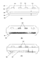
[第一の実施の形態]
本発明の第一の実施例を図5(a)に示す。図5(a)は本発明の一例として構成したシールド付きペアケーブルの断面図である。また、図4(a)は、図5(a)との比較対象になる従来技術によるシールド付きペアケーブルの断面図である。
[First embodiment]
A first embodiment of the present invention is shown in FIG. FIG. 5A is a cross-sectional view of a shielded pair cable configured as an example of the present invention. FIG. 4A is a cross-sectional view of a shielded pair cable according to the prior art which is a comparison object with FIG.
図4(a)の従来技術によるシールド付きペアケーブルにおいて、101は周囲の媒質、102はシールド導体、103は誘電体、106と107は本来目的とする信号伝送を行うための信号導体を表す。
In the shielded pair cable according to the prior art shown in FIG. 4A,
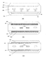
図4(b)は、従来技術のシールド付きペアケーブルについて、直流付近の周波数における、導体内部の電流分布を図示したものである。信号電流123は、「直流電流は電気抵抗を最小にする経路を流れる」という一般法則にしたがって、信号導体106と107の断面をほぼ均一に流れる。電流121は、信号電流123が流れることによってシールド導体内に誘起される電流であって、電流122は、主に送信側電子回路の内部や送信側電子回路とシールド導体の接続部で生じる不要電流を表している。シールド層の信号電流によって誘起された電流121は、ペアケーブルの奇モードの電界の空間分布に対応して角度方向には不均一な分布を持つが、直流付近の周波数においては表皮深さが大きいため、半径方向にはシールド導体の内側表面からシールド導体の内部に深く侵入しうる。また、不要電流122も、直流付近の周波数においては導体内部に深く侵入する。このため、直流付近の周波数においては、シールド導体を上述の誘起電流121と不要電流122が空間的に重なり合った形で流れることになる。
FIG. 4 (b) illustrates the current distribution inside the conductor at a frequency in the vicinity of a direct current for a shielded pair cable according to the prior art. The signal current 123 flows substantially uniformly in the cross sections of the
図4(c)は、従来技術のシールド付きペアケーブルについて、高周波における導体内部の電流分布を図示したものである。信号電流143は、表皮効果と近接効果のために信号導体106と107の対抗する面に集中する。また、シールド導体内の電流は、数式(1)の表皮効果のために、シールド導体表面の表皮深さδ(νmin)程度の厚みの領域に集中する。信号電流によってシールド導体内部に誘起される電流141は、ペアケーブルの奇モードの電界に対応して角度方向には不均一な空間分布を持ち、かつ信号導体上の電荷分布が作る電界を遮蔽するようにシールド導体の内側表面に集中する。一方、不要電流142は「高周波電流はインピーダンスを最小にする経路を流れる」という一般法則にしたがって、シールド導体の外側表面に集中する。
FIG. 4C illustrates the current distribution inside the conductor at high frequency for the shielded pair cable of the prior art. The signal current 143 is concentrated on the opposing surfaces of the
図5(a)は、本発明の一実施例として構成したシールド付きペアケーブルの断面図であって、104は高損失導体層、105は低損失導体層を表している。本実施例においては、従来不要電流の高周波成分が流れていた部分に高損失導体層104を設けたことにより、不要電流の高周波成分を効率的に減衰させて、シールド層からの不要電磁界の発生を抑制できるようになった。
FIG. 5A is a cross-sectional view of a shielded pair cable configured as an embodiment of the present invention, in which 104 represents a high-loss conductor layer and 105 represents a low-loss conductor layer. In the present embodiment, the high
図5(a)において、低損失導体層105の材料としては、例えば、通常信号導体やシールド導体として用いられる銅、銀、アルミ、金などの導電率の大きい金属や、それらの合金、またはそれらの金属を層状構造にしたものを用いても良い。また、高損失導体層104の材料としては、低損失導体層105に比べて導電率が小さい材料を用いることが可能であり、例えば、スズ、ニッケル、クロム、鉄、ビスマス、チタン、カーボンなどの金属や半金属、導電性ポリマー、導電率の大きい半導体材料、はんだ合金、ステンレス、炭素鋼、フェライト、およびそれらの材料を層状構造にしたものなどを用いてもよい。
In FIG. 5A, examples of the material of the low-
高損失導体層104と低損失導体層105からなる層状構造の構成手段としては、低損失導体からなる一本の円筒導体の表面に高損失導体材料をメッキしても良いし、低損失導体からなる一本の円筒導体の表面に高損失導体材料を材料とする複数の円柱導体からなる撚り線層を形成しても良いし、低損失導体を材料とする一本の円筒導体の表面に高損失導体を材料とする金属箔を巻き付けても良いし、低損失導体を材料とする複数の円柱導体からなる撚り線層の外側に、高損失導体を材料とする複数の円柱導体からなる撚り線層を形成しても良いし、低損失導体を材料とする複数の円柱導体からなる撚り線層の外側に高損失導体をメッキしても良いし、低損失導体を材料とする複数の円柱導体からなる撚り線層の外側に、高損失導体を材料とする金属箔を巻き付けても良い。
As a means for forming a layered structure composed of the high-
また、信号導体106、107は、一本の導体円柱や導体円筒によって構成しても良いし、可とう性を持たせるために複数の導体円柱や導体円筒からなる撚り線構造によって構成しても良い。図5(a)では信号導体の数を二本としているが、本発明の要点はシールド導体の構造にあるので、信号導体の数は二本以上であっても良い。さらに、図5(a)の断面図に対応する長手方向の構造は、一様でもよく、また信号導体の配置にねじりを加えた所謂ツイストペア構造であっても良い。
Further, the
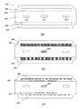
以下、本実施例のシールド付きペアケーブルの機能を、直流付近に近い周波数と、高周波領域に分けて詳しく説明する。図5(b)は、本発明のシールド付きペアケーブルの、直流付近の周波数における導体内部の電流分布を図示したものである。シールド導体には、信号電流に伴って誘起される電流121と不要電流122が流れているので、高損失導体層104を設けると両者が影響を受けることになる。しかし、直流付近の周波数においては、どちらの電流もシールド導体の内部に深く侵入しているので、高損失導体層の断面積をαH、低損失導体層の断面積をαLとすると、高損失導体層104を設けたことによる直流抵抗の変化はおよそ(αH+αL)/αL倍になる。ここで、不要電磁界を抑制したい周波数が十分高い周波領域にある場合には、対応する表皮厚さが小さいので、シールド導体厚を適切に設定することによって(αH+αL)/αLを、個々の応用の目的から見て十分1に近い値にすることが可能である。したがって、直流付近の周波数においては、高損失導体層104を設けたことによる、信号電流に伴って誘起される電流121と不要電流122への影響は十分に小さくすることができる。
Hereinafter, the function of the shielded pair cable according to the present embodiment will be described in detail for a frequency close to a direct current and a high frequency region. FIG. 5B illustrates the current distribution inside the conductor at a frequency near the direct current of the shielded pair cable of the present invention. Since the current 121 induced by the signal current and the unnecessary current 122 flow through the shield conductor, both are affected when the high
一方、図5(c)は、本発明のシールド付きペアケーブルの、高い周波数、すなわち不要電磁界の発生を抑えたい周波数領域の下限値νminにおける、導体内部の電流分布を図示したものである。高周波においては、信号電流に伴って誘起される電流141がシールド導体の内側表面に集中するため、高損失導体層104の厚みが低損失導体層105の厚みよりも小さければ、高損失導体層104を設けたことによる、誘起電流141への影響は存在しない。
On the other hand, FIG. 5C illustrates the current distribution inside the conductor at the high frequency, that is, the lower limit value ν min of the frequency region where it is desired to suppress the generation of unwanted electromagnetic fields, in the shielded pair cable of the present invention. . At high frequencies, the current 141 induced with the signal current concentrates on the inner surface of the shield conductor. Therefore, if the thickness of the high
また、高周波においては、不要電流はシールド導体の外側表面の電流経路144を流れるほかないが、電流経路144が高損失導体層104によって形成されているために、不要電流は伝送方向に急速に減衰してしまい、実際にはほとんど流れることができない。高損失導体層104の電気抵抗率をρH、低損失導体層105の電気抵抗率をρLとすると、高損失導体層104を設けた場合の不要電流の高周波成分の減衰率は、高損失導体層がない場合のおよそρH/ρL倍になる。ρH/ρL≫1であるような材料の組合せを用いれば、高損失導体層を設けた部分(電流経路144)を流れる電流は十分な距離を伝播した後では十分に小さくなるので、本発明の構造によって、不要電磁界の原因になる不要電流の高周波成分を選択的に除去することができる。なお、以上はあくまで本発明の一実施例を示したものであり、本発明の有効範囲を限定するものではない。
At high frequencies, the unnecessary current flows through the
[第二の実施の形態]
本発明の第二の実施例の断面図を図7(a)に示す。図7(a)は本発明の一例として構成した同軸ケーブルの断面図である。また、図6(a)は図7(a)と比較される従来技術による同軸ケーブルの断面図である。
[Second Embodiment]
A cross-sectional view of the second embodiment of the present invention is shown in FIG. FIG. 7A is a cross-sectional view of a coaxial cable configured as an example of the present invention. FIG. 6A is a cross-sectional view of a conventional coaxial cable compared with FIG. 7A.
従来技術による同軸ケーブルを示した図6(a)において、201は周囲の媒質、202は外部導体、203は誘電体、206は内部導体である。同軸ケーブルにおいては、信号電流が内部導体と外部導体を流れると同時に、外部導体はシールド導体としての役割も兼ねる。 In FIG. 6A showing a coaxial cable according to the prior art, 201 is a surrounding medium, 202 is an outer conductor, 203 is a dielectric, and 206 is an inner conductor. In a coaxial cable, a signal current flows through an inner conductor and an outer conductor, and at the same time, the outer conductor also serves as a shield conductor.
図6(b)は、従来技術の同軸ケーブルについて、直流付近の周波数における、導体内部の電流分布を図示したものである。信号電流223は、「直流電流は電気抵抗を最小にする経路を流れる」という一般法則にしたがって、内部導体206の断面をほぼ均一に流れる。電流221は外部導体を流れる信号電流であって、内部導体を流れる往路電流に対する帰路電流である。
FIG. 6B illustrates the current distribution inside the conductor at a frequency in the vicinity of the direct current of the coaxial cable of the prior art. The signal current 223 flows substantially uniformly in the cross section of the
また、電流222は、主に送信側電子回路の内部や送信側電子回路と外部導体の接続部で生じる不要電流を表している。外部導体を流れる信号電流221は、「直流電流は電気抵抗を最小にする経路を流れる」という一般法則にしたがって、外部導体の内部をほぼ均一に流れる。また、不要電流222も、直流付近の周波数においては外部導体の内部に深く侵入している。このため、直流付近の周波数においては、外部導体を、上述の信号電流221と不要電流222が空間的に重なり合った形で流れることになる。信号電流221と不要電流222は、それぞれ、同軸ケーブルのノーマルモード電流とコモンモード電流と呼ばれることもある。 The current 222 represents an unnecessary current mainly generated in the transmission-side electronic circuit or in the connection portion between the transmission-side electronic circuit and the external conductor. The signal current 221 flowing through the outer conductor flows substantially uniformly inside the outer conductor in accordance with the general rule that “DC current flows through a path that minimizes electrical resistance”. The unnecessary current 222 also penetrates deeply into the outer conductor at a frequency near DC. For this reason, at the frequency near the direct current, the signal current 221 and the unnecessary current 222 flow through the outer conductor in a spatially overlapping manner. The signal current 221 and the unnecessary current 222 may be called a normal mode current and a common mode current of the coaxial cable, respectively.
図6(c)は、従来技術の同軸ケーブルについて、高周波における導体内部の電流分布を図示したものである。内部導体の信号電流243は、表皮効果のために内部導体206の表面に集中する。また、外部導体内部の電流も、表皮効果のために外部導体表面の表皮深さδ(νmin)程度の厚みの領域に集中する。外部導体を流れる信号電流241は、内部導体の信号電流243と電気的に結合しているため、外部導体の内側表面に集中する。一方、不要電流242は「高周波電流はインピーダンスを最小にする経路を流れる」という一般法則にしたがって、外部導体の外側表面に集中する。
FIG. 6C illustrates the current distribution inside the conductor at a high frequency for the coaxial cable of the prior art. The
図7(a)は、本発明の一実施例として構成した同軸ケーブルの断面図であって、204は高損失導体層、205は低損失導体層を表している。本実施例においては、従来不要電流の高周波成分が流れていた部分に高損失導体層204を設けたことによって、不要電流の高周波成分を効率的に減衰させて、外部導体からの不要電磁界の発生を抑制できるようになった。
FIG. 7A is a cross-sectional view of a coaxial cable configured as an embodiment of the present invention, in which 204 represents a high-loss conductor layer and 205 represents a low-loss conductor layer. In the present embodiment, the high
図7(a)において、低損失導体層205の材料としては、例えば、通常信号導体や外部導体として用いられる銅、銀、アルミ、金などの導電率の大きい金属や、それらの合金、またはそれらの金属を層状構造にしたものを用いても良い。また、高損失導体層204の材料としては、低損失導体層205に比べて導電率が小さい材料を用いることが可能であり、例えば、スズ、ニッケル、クロム、鉄、ビスマス、チタン、カーボンなどの金属や半金属、導電性ポリマー、導電率の大きい半導体材料、はんだ合金、ステンレス、炭素鋼、フェライト、およびそれらの材料を層状構造にしたものなどを用いてもよい。
In FIG. 7A, the material of the low-
高損失導体層204と低損失導体層205からなる層状構造の構成手段としては、低損失導体からなる一本の円筒導体の表面に高損失導体材料をメッキしても良いし、低損失導体からなる一本の円筒導体の表面に高損失導体材料を材料とする複数の円柱導体からなる撚り線層を形成しても良いし、低損失導体を材料とする一本の円筒導体の表面に高損失導体を材料とする金属箔を巻き付けても良いし、低損失導体を材料とする複数の円柱導体からなる撚り線層の外側に、高損失導体を材料とする複数の円柱導体からなる撚り線層を形成しても良いし、低損失導体を材料とする複数の円柱導体からなる撚り線層の外側に高損失導体をメッキしても良いし、低損失導体を材料とする複数の円柱導体からなる撚り線層の外側に、高損失導体を材料とする金属箔を巻き付けても良い。
As a means for forming a layered structure composed of the high-
また、内部導体206は、一本の導体円柱や導体円筒によって構成しても良いし、可とう性を持たせるために複数の導体円柱や導体円筒からなる撚り線構造によって構成しても良い。図7(a)では信号導体の数を一本としているが、本発明の要点は外部導体の構造にあるので、信号電流の往路導体になる内部導体の数は、一本以上であっても良い。
Further, the
さらに、図7(a)の断面図に対応する長手方向の構造は、一様でもよく、また信号導体の配置にねじりを加えた所謂ツイストペア構造であっても良い。 Furthermore, the structure in the longitudinal direction corresponding to the cross-sectional view of FIG. 7A may be uniform, or may be a so-called twisted pair structure in which the arrangement of signal conductors is twisted.
以下、本実施例の同軸ケーブルの機能を、直流付近に近い周波数と、高周波領域に分けて詳しく説明する。 Hereinafter, the function of the coaxial cable of the present embodiment will be described in detail by dividing it into a frequency close to DC and a high frequency region.
図7(b)は、本発明の同軸ケーブルの、直流付近の周波数における導体内部の電流分布を図示したものである。外部導体には、信号電流221と不要電流222が流れているので、高損失導体層204を設けると両者が影響を受けることになる。しかし、直流付近の周波数においては、どちらの電流も外部導体の内部に深く侵入しているので、高損失導体層と低損失導体層の断面積をαHおよびαLとすると、高損失導体層204を設けたことによる直流抵抗の変化はおよそ(αH+αL)/αL倍になる。ここで、不要電磁界を抑制したい周波数が十分高い周波領域にある場合には、対応する表皮厚さが小さいので、外部導体の厚さを適切に設定することによって(αH+αL)/αLを、個々の応用の目的から見て十分1に近い値にすることが可能である。したがって、直流付近の周波数においては、高損失導体層204を設けたことによる、信号電流221と不要電流222への影響は十分に小さくすることができる。
FIG. 7B illustrates the current distribution inside the conductor at a frequency near the direct current of the coaxial cable of the present invention. Since the signal current 221 and the unnecessary current 222 flow in the external conductor, both are affected when the high-
一方、図7(c)は、本発明の同軸ケーブルの、高い周波数、すなわち不要電磁界の発生を抑えたい周波数領域の下限値νminにおける、導体内部の電流分布を図示したものである。 On the other hand, FIG. 7C illustrates the current distribution inside the conductor at the lower limit value ν min of the high frequency, that is, the frequency region where it is desired to suppress the generation of unwanted electromagnetic fields, in the coaxial cable of the present invention.
高周波においては、外部導体を流れる信号電流241が外部導体の内側表面に集中するため、高損失導体層204の厚みが低損失導体層205の厚みよりも小さければ、高損失導体層204を設けたことによる、信号電流241への影響は存在しない。また、高周波においては、不要電流は外部導体の外側表面の電流経路244を流れるほかないが、電流経路244が高損失導体層204によって形成されているので、不要電流は伝送方向に急速に減衰してしまい、実際にはほとんど流れることができない。
At high frequencies, the signal current 241 flowing through the outer conductor is concentrated on the inner surface of the outer conductor. Therefore, if the thickness of the high
高損失導体層204と低損失導体層205の電気抵抗率をρHおよびρLとすると、高損失導体層204を設けた場合の不要電流の高周波成分の減衰率は、高損失導体層がない場合のおよそρH/ρL倍になる。ρH/ρL≫1であるような材料の組合せを用いれば、外部導体の外側表面の電流経路244を流れる不要電流は、十分な距離を伝播した後では十分に小さくなるので、本発明の構造によって、不要電磁界の原因になる不要電流の高周波成分を選択的に除去することができる。なお、以上はあくまで本発明の一実施例を示したものであり、本発明の有効範囲を限定するものではない。
When the electrical resistivity of the high-
[第三の実施の形態]
本発明の第三の実施例の断面図を図9(a)に示す。図9(a)は本発明の一例として、プリント配線基板上に差動ストリップ線路を構成したものの断面図である。また、図8(a)は図9(a)と比較される、従来技術によるプリント配線基板の断面図である。
[Third embodiment]
A sectional view of the third embodiment of the present invention is shown in FIG. FIG. 9A is a cross-sectional view of a differential strip line formed on a printed wiring board as an example of the present invention. FIG. 8A is a cross-sectional view of a printed wiring board according to the prior art, compared with FIG. 9A.
従来技術によるプリント配線基板を示した図8(a)において、301は周囲の媒質、302はレジスト、303はグランド導体、306は誘電体、311と312は信号導体、313は周囲にある信号導体以外の配線パターンである。プリント配線基板上の差動ストリップ線路においては、信号導体311、312に近接して配置されたグランド導体が、下方への不要電磁界の漏出を防ぎ、さらに信号導体と逆符号の電磁界を発生して不要電磁界を弱めるためのシールド層として機能する。
8A showing a printed wiring board according to the prior art, 301 is a surrounding medium, 302 is a resist, 303 is a ground conductor, 306 is a dielectric, 311 and 312 are signal conductors, and 313 is a surrounding signal conductor. It is a wiring pattern other than. In the differential strip line on the printed circuit board, the ground conductor arranged in the vicinity of the
図8(b)は、従来技術のプリント配線基板について、直流付近の周波数における、導体内部の電流分布を図示したものである。信号電流323は、「直流電流は電気抵抗を最小にする経路を流れる」という一般法則にしたがって、信号導体311と312の断面をほぼ均一に流れる。電流321は、差動ストリップ線路の信号導体311と312に信号電流323が流れることによってグランド導体内に誘起される電流であって、電流322は、主に送信側電子回路の内部や電子回路とプリント配線基板の接続部で生じる不要電流を表している。グランド導体内の誘起電流321は、差動ストリップ線路の電界分布に対応して、信号電流323のペア内の位相関係に依存した横方向に不均一な分布を持つが、直流付近の周波数においては表皮深さが大きいので、深さ方向にはグランド導体内部に深く侵入しうる。また、不要電流322も、直流付近の周波数においてはグランド導体内部に深く侵入する。このため、直流付近の周波数においては、グランド導体内部を、上述の誘起電流321と不要電流322が空間的に重なり合った形で流れることになる。
FIG. 8B illustrates the current distribution inside the conductor at a frequency in the vicinity of a direct current for a printed wiring board according to the prior art. The signal current 323 flows substantially uniformly through the cross sections of the
図8(c)は、従来技術のプリント配線基板の、高周波における導体内部の電流分布を図示したものである。信号電流343は、表皮効果と近接効果によって信号導体311と312の下側表面、中でもコーナー部分に集中する。また、グランド導体を流れる二種類の電流も、表皮効果のためにグランド導体表面の表皮深さδ(νmin)程度の厚みの領域に集中する。二種類の電流のうち、信号電流によって誘起される電流341は、差動ストリップ線路の電界分布に応じた横方向に不均一な空間分布を持ち、かつ信号導体上の電荷分布が作る電界を遮蔽するように、グランド導体303の信号導体311、312に近い側の表面に集中する。一方、不要電流342は「高周波電流はインピーダンスを最小にする経路を流れる」という一般法則にしたがって、グランド導体303の、信号導体311、312から遠い側の表面に集中する。
FIG. 8C illustrates the current distribution inside the conductor at a high frequency of the printed circuit board according to the prior art. The signal current 343 is concentrated on the lower surfaces of the
図9(a)は、本発明の一実施例として構成したプリント配線基板上の差動ストリップ線路の断面図であって、304は高損失導体層、305は低損失導体層を表している。本実施例においては、従来不要電流の高周波成分が流れていた部分に高損失導体層304を設けたことにより、不要電流の高周波成分を効率的に減衰させて、グランド導体からの不要電磁界の発生を抑制できるようになった。
FIG. 9A is a cross-sectional view of a differential strip line on a printed wiring board configured as an embodiment of the present invention, where 304 indicates a high-loss conductor layer and 305 indicates a low-loss conductor layer. In this embodiment, the high
図9(a)において、低損失導体層305の材料としては、例えば、通常導体材料として用いられる銅に加え、銀、アルミ、金などの導電率の大きい金属や、それらの合金、またはそれらの金属を層状構造にしたものを用いても良い。また、高損失導体層304の材料としては、低損失導体層305に比べて導電率が小さい材料を用いることが可能であり、例えば、スズ、ニッケル、クロム、鉄、ビスマス、チタン、カーボンなどの金属や半金属、導電性ポリマー、導電率の大きい半導体材料、はんだ合金、ステンレス、炭素鋼、フェライト、およびそれらの材料を層状構造にしたものなどを用いてもよい。誘電体306の材料としては、通常のリジッドプリント配線基板やフレキシブルプリント配線基板に用いられている材料をそのまま用いることができる。例を挙げれば、ガラスエポキシ樹脂、テフロン(登録商標)、アルミナ、サファイア、ポリイミド、液晶ポリマーなどである。また、レジスト302は無くても良い。
In FIG. 9A, as a material of the low-
高損失導体層304と低損失導体層305からなる層状構造の構成手段としては、低損失導体の表面に高損失導体材料をメッキしても良い。また、図9(a)では差動ストリップ線路の例を示したが、本発明の要点はグランド導体の構造にあるので、信号配線は差動ストリップ線路以外の線路であっても良く、例えば導体配列は所謂GSSG配列などのより複雑なものであって良く、線路構造もストリップ線路以外のコプレーナー線路などであっても良い。また、図9(a)では一層の信号層と一層のグランド層からなる二層プリント配線基板の例を示したが、多層プリント配線基板でも、信号配線層と隣接するグランド配線層の、信号配線層から遠い側の表面に高損失導体層を設ければ本発明の効果がえられることは明白である。
As a means for forming a layered structure composed of the high-
以下、本実施例のプリント配線基板の機能を、直流付近に近い周波数と、高周波領域に分けて詳しく説明する。 Hereinafter, the function of the printed wiring board of the present embodiment will be described in detail by dividing it into a frequency close to DC and a high frequency region.
図9(b)は、本発明のプリント配線基板の、直流付近の周波数における導体内部の電流分布を図示したものである。グランド導体には、信号電流に伴って誘起される電流321と不要電流322が流れているので、高損失導体層304を設けると両者が影響を受けることになる。しかし、直流付近の周波数においては、どちらの電流もグランド導体の内部に深く侵入しているので、高損失導体層の断面積をαH、低損失導体層の断面積αLとすると、高損失導体層304を設けたことによる直流抵抗の変化はおよそ(αH+αL)/αL倍となる。ここで、不要電磁界を抑制したい周波数が十分高い周波領域にある場合には、対応する表皮厚さが小さいので、グランド導体厚を適切に設定することによって(αH+αL)/αLを、個々の応用の目的から見て十分1に近い値にすることが可能である。したがって、直流付近の周波数においては、高損失導体層304を設けたことによる、信号電流に伴って誘起される電流321と不要電流322への影響は十分に小さくすることができる。
FIG. 9B illustrates the current distribution inside the conductor at a frequency near the direct current of the printed wiring board of the present invention. Since a current 321 and an unnecessary current 322 induced along with a signal current flow through the ground conductor, both are affected when the high-
一方、図9(c)は、本発明のプリント配線基板の、高い周波数、すなわち不要電磁界の発生を抑えたい周波数領域の下限値νminにおける、導体内部の電流分布を図示したものである。高周波においては、信号電流に伴って誘起される電流341が、グランド導体の、信号導体に近い側の表面に集中するために、高損失導体層304の厚みが低損失導体層305の厚みよりも小さければ、高損失導体層304を設けたことによる、誘起電流341への影響は存在しない。また、高周波においては、不要電流は、グランド導体の信号導体から遠い側の表面(電流経路344)を流れるほかないが、電流経路344が高損失導体層304によって形成されているので、不要電流は伝送方向に急速に減衰してしまい、実際にはほとんど流れることができない。高損失導体層304と低損失導体層305の電気抵抗率をρHおよびρLとすると、高損失導体層304を設けた場合の不要電流の高周波成分の減衰率は、高損失導体層がない場合のおよそρH/ρL倍になる。ρH/ρL≫1であるような材料の組合せを用いれば、高損失導体層を設けた部分(電流経路344)を流れる電流は十分な距離を伝播した後では十分に小さくなるので、本発明の構造によって、不要電磁界の原因になる不要電流の高周波成分を選択的に除去することができる。なお、以上はあくまで本発明の一実施例を示したものであり、本発明の有効範囲を限定するものではない。
On the other hand, FIG. 9C illustrates the current distribution inside the conductor at the high frequency, that is, the lower limit value ν min of the frequency region where it is desired to suppress the generation of unwanted electromagnetic fields, in the printed wiring board of the present invention. At high frequencies, the current 341 induced by the signal current concentrates on the surface of the ground conductor on the side close to the signal conductor, so the thickness of the high
[第四の実施の形態]
本発明の第四の実施例の断面図を図11(a)に示す。図11(a)は本発明の一例として、プリント配線基板上に差動マイクロストリップ線路を構成したものの断面図である。また、図10(a)は図11(a)と比較される、従来技術によるプリント配線基板の断面図である。
[Fourth embodiment]
A cross-sectional view of the fourth embodiment of the present invention is shown in FIG. FIG. 11A is a sectional view of a differential microstrip line formed on a printed wiring board as an example of the present invention. FIG. 10A is a cross-sectional view of a printed wiring board according to the prior art, compared with FIG.
従来の技術を示した図10(a)において、301は周囲の媒質、302はレジスト、303はグランド導体、306は誘電体、311と312は信号導体、313は周囲にある信号導体以外の配線パターンである。プリント配線基板上の差動マイクロストリップ線路においては、信号導体311、312の上下に近接して配置されたグランド導体が、不要電磁界の漏出を防ぎ、さらに信号導体と逆符号の電磁界を発生して不要電磁界を弱めるためのシールド層として機能する。
In FIG. 10A showing the prior art, 301 is a surrounding medium, 302 is a resist, 303 is a ground conductor, 306 is a dielectric, 311 and 312 are signal conductors, and 313 is a wiring other than the surrounding signal conductors. It is a pattern. In the differential microstrip line on the printed circuit board, the ground conductors arranged close to the top and bottom of the
図11(a)は、本発明の一実施例として構成したプリント配線基板上の差動ストリップ線路の断面図であって、304は高損失導体層、305は低損失導体層を表している。本実施例においては、従来不要電流の高周波成分が流れていた部分に高損失導体層304を設けたことにより、不要電流の高周波成分を効率的に減衰させて、シールド層からの不要電磁界の発生を抑制できるようになった。図11(a)の構成材料の例、層状構造の構成手段の例、構造変形例などは、実施例三の場合と同様である。本実施例は実施例三と類似しているので、機能などの詳細の説明は省略する。
FIG. 11A is a cross-sectional view of a differential strip line on a printed wiring board configured as an embodiment of the present invention, where 304 indicates a high-loss conductor layer and 305 indicates a low-loss conductor layer. In this embodiment, the high
[第五の実施の形態]
本発明の第五の実施例の断面図を図13(a)に示す。図13(a)は本発明の一例として、プリント配線基板上にストリップ線路を構成したものの断面図である。また、図12(a)は図13(a)と比較される、従来技術によるプリント配線基板の断面図である。
[Fifth embodiment]
A cross-sectional view of the fifth embodiment of the present invention is shown in FIG. FIG. 13A is a cross-sectional view of a strip line formed on a printed wiring board as an example of the present invention. FIG. 12A is a cross-sectional view of a printed wiring board according to the prior art, compared with FIG.
従来技術によるプリント配線基板を示した図12(a)において、401は周囲の媒質、402はレジスト、403はグランド導体、406は誘電体、411は信号導体、413は周囲にある信号導体以外の配線パターンである。プリント配線基板上のストリップ線路においては、信号導体411に近接して配置されたグランド導体が、信号導体を流れる往路電流に対応した帰路電流を流すとともに、下方への不要電磁界の漏出を防ぎ、さらに信号導体と逆符号の電磁界を発生して不要電磁界を弱めるためのシールド層としての機能を持つ。
In FIG. 12A showing a printed wiring board according to the prior art, 401 is a surrounding medium, 402 is a resist, 403 is a ground conductor, 406 is a dielectric, 411 is a signal conductor, 413 is a signal conductor other than the surrounding signal conductor. It is a wiring pattern. In the strip line on the printed circuit board, the ground conductor disposed in the vicinity of the
図12(b)は、従来技術のプリント配線基板について、直流付近の周波数における導体内部の電流分布を図示したものである。信号電流423は、「直流電流は電気抵抗を最小にする経路を流れる」という一般法則にしたがって、信号導体411の断面をほぼ均一に流れる。電流421は、グランド導体を流れるリターン電流であって、電流422は、主に送信側電子回路の内部や電子回路とプリント配線基板の接続部で生じる不要電流を表している。グランド導体を流れるリターン電流421は、横方向に不均一な分布を持つが、直流付近の周波数においては表皮深さが大きいので深さ方向にはグランド導体内部に深く侵入している。また、不要電流422も、直流付近の周波数においてはグランド導体内部に深く侵入する。このため、直流付近の周波数においては、グランド導体内部を、リターン電流421と不要電流422が空間的に重なり合った形で流れることになる。
FIG. 12B illustrates the current distribution inside the conductor at a frequency near the direct current for a printed wiring board according to the prior art. The signal current 423 flows substantially uniformly in the cross section of the
図12(c)は、従来技術のプリント配線基板の、高周波における導体内部の電流分布を図示したものである。信号電流443は、表皮効果によって信号導体411の下側表面、中でもコーナー部分に集中する。また、グランド導体を流れる二種類の電流も、表皮効果のためにグランド導体表面の表皮深さδ(νmin)程度の厚みの領域に集中する。二種類の電流のうち、リターン電流441は、信号導体上の電荷分布が作る電界を遮蔽するように、グランド導体403の信号導体411に近い側の表面に集中する。一方、不要電流442は「高周波電流はインピーダンスを最小にする経路を流れる」という一般法則にしたがって、グランド導体403の、信号導体411から遠い側の表面に集中する。
FIG. 12C illustrates the current distribution inside the conductor at a high frequency of the printed circuit board according to the prior art. The signal current 443 is concentrated on the lower surface of the
図13(a)は、本発明の一実施例として構成したプリント配線基板上のストリップ線路の断面図であって、404は高損失導体層、405は低損失導体層を表している。本実施例においては、従来不要電流の高周波成分が流れていた部分に高損失導体層404を設けたことにより、不要電流の高周波成分を効率的に減衰させて、グランド導体からの不要電磁界の発生を抑制できるようになった。
FIG. 13A is a cross-sectional view of a strip line on a printed wiring board configured as an embodiment of the present invention, where 404 indicates a high-loss conductor layer and 405 indicates a low-loss conductor layer. In this embodiment, the high-
図13(a)において、低損失導体層405の材料としては、例えば、通常導体材料として用いられる銅に加え、銀、アルミ、金などの導電率の大きい金属や、それらの合金、またはそれらの金属を層状構造にしたものを用いても良い。また、高損失導体層404の材料としては、低損失導体層405に比べて導電率が小さい材料を用いることが可能であり、例えば、スズ、ニッケル、クロム、鉄、ビスマス、チタン、カーボンなどの金属や半金属、導電性ポリマー、導電率の大きい半導体材料、はんだ合金、ステンレス、炭素鋼、フェライト、およびそれらの材料を層状構造にしたものなどを用いてもよい。誘電体406の材料としては、通常のリジッドプリント配線基板やフレキシブルプリント配線基板に用いられている材料をそのまま用いることができる。例を挙げれば、ガラスエポキシ樹脂、テフロン(登録商標)、アルミナ、サファイア、ポリイミド、液晶ポリマーなどである。また、レジスト402は無くても良い。
In FIG. 13 (a), as a material of the low-
高損失導体層404と低損失導体層405からなる層状構造の構成手段としては、低損失導体の表面に高損失導体材料をメッキしても良い。また、図13(a)ではストリップ線路の例を示したが、本発明の要点はグランド導体の構造にあるので、信号配線はストリップ線路以外の線路であっても良い。
As a means for forming a layered structure including the high-
また、図13(a)では一層の信号層と一層のグランド層からなる二層プリント配線基板の例を示したが、多層プリント配線基板でも、信号配線層と隣接するグランド配線層の、信号配線層から遠い側の表面に高損失導体層を設ければ本発明の効果がえられることは明白である。また、グランド層ではなく、信号配線層と隣接する電源層の信号配線層から遠い側の表面に高損失導体層を設けることによっても本発明で述べられている効果をえることができる。 FIG. 13A shows an example of a two-layer printed wiring board composed of a single signal layer and a single ground layer. However, in the multilayer printed wiring board, the signal wiring of the ground wiring layer adjacent to the signal wiring layer is also shown. It is obvious that the effect of the present invention can be obtained by providing a high-loss conductor layer on the surface far from the layer. Further, the effect described in the present invention can also be obtained by providing a high-loss conductor layer on the surface of the power supply layer adjacent to the signal wiring layer far from the signal wiring layer instead of the ground layer.
以下、本実施例のプリント配線基板の機能を、直流付近に近い周波数と、高周波領域に分けて詳しく説明する。図13(b)は、本発明のプリント配線基板の、直流付近の周波数における導体内部の電流分布を図示したものである。グランド導体には、リターン電流421と不要電流422が流れているので、高損失導体層404を設けると両者が影響を受けることになる。しかし、直流付近の周波数においては、どちらの電流もグランド導体の内部に深く侵入しているので、高損失導体層と低損失導体層の断面積をαHおよびαLとすると、高損失導体層404を設けたことによる直流抵抗の変化はおよそ(αH+αL)/αL倍となる。ここで、不要電磁界を抑制したい周波数が十分高い周波領域にある場合には、対応する表皮厚さが小さいので、グランド導体厚を適切に設定することによって(αH+αL)/αLを、個々の応用の目的から見て十分1に近い値にすることが可能である。したがって、直流付近の周波数においては、高損失導体層404を設けたことによる、リターン電流421と不要電流422への影響は十分に小さくすることができる。
Hereinafter, the function of the printed wiring board of the present embodiment will be described in detail by dividing it into a frequency close to DC and a high frequency region. FIG. 13B illustrates the current distribution inside the conductor at a frequency near the direct current of the printed wiring board of the present invention. Since the return current 421 and the unnecessary current 422 flow through the ground conductor, the provision of the high-
一方、図13(c)は、本発明のプリント配線基板の、高い周波数、すなわち不要電磁界の発生を抑えたい周波数領域の下限値νminにおける、導体内部の電流分布を図示したものである。高周波においては、リターン電流441が、グランド導体の、信号導体に近い側の表面に集中するために、高損失導体層404の厚みが低損失導体層405の厚みよりも小さければ、高損失導体層404を設けたことによるリターン電流341への影響は存在しない。また、高周波においては、不要電流は、グランド導体の信号導体から遠い側の表面444を流れるほかないが、電流経路444が高損失導体層404によって形成されているので、不要電流は伝送方向に急速に減衰してしまい、実際にはほとんど流れることができない。
On the other hand, FIG. 13C illustrates the current distribution inside the conductor at the high frequency, that is, the lower limit value ν min of the frequency region where it is desired to suppress the generation of unwanted electromagnetic fields, in the printed wiring board of the present invention. At high frequencies, the return current 441 concentrates on the surface of the ground conductor on the side closer to the signal conductor. Therefore, if the thickness of the high
高損失導体層404と低損失導体層405の電気抵抗率をρHおよびρLとすると、高損失導体層404を設けた場合の不要電流の高周波成分の減衰率は、高損失導体層がない場合のおよそρH/ρL倍になる。ρH/ρL≫1であるような材料の組合せを用いれば、高損失導体層を設けた部分444を流れる電流は十分な距離を伝播した後では十分に小さくなるので、本発明の構造によって、不要電磁界の原因になる不要電流の高周波成分を選択的に除去することができる。なお、以上はあくまで本発明の一実施例を示したものであり、本発明の有効範囲を限定するものではない。
If the electrical resistivity of the high-
[第六の実施の形態]
本発明の第六の実施例の断面図を図15(a)に示す。図15(a)は本発明の一例として、プリント配線基板にマイクロストリップ線路を構成したものの断面図である。また、図14(a)は図15(a)と比較される、従来技術によるプリント配線基板の断面図である。
[Sixth embodiment]
A sectional view of the sixth embodiment of the present invention is shown in FIG. FIG. 15A is a cross-sectional view of a microstrip line formed on a printed wiring board as an example of the present invention. FIG. 14A is a cross-sectional view of a printed wiring board according to the prior art, compared with FIG.
従来の技術を示した図14(a)において、401は周囲の媒質、402はレジスト、403はグランド導体、406は誘電体、411は信号導体、413は周囲にある信号導体以外の配線パターンである。プリント配線基板上のマイクロストリップ線路においては、信号導体411の上下に近接して配置されたグランド導体403が、不要電磁界の漏出を防ぎ、さらに信号導体と逆符号の電磁界を発生して不要電磁界を弱めるためのシールド層として機能する。
In FIG. 14A showing the prior art, 401 is a surrounding medium, 402 is a resist, 403 is a ground conductor, 406 is a dielectric, 411 is a signal conductor, and 413 is a wiring pattern other than the surrounding signal conductor. is there. In the microstrip line on the printed wiring board, the
図15(a)は、本発明の一実施例として構成したプリント配線基板上のストリップ線路の断面図であって、404は高損失導体層、405は低損失導体層を表している。本実施例においては、従来不要電流の高周波成分が流れていた部分に高損失導体層404を設けたことにより、不要電流の高周波成分を効率的に減衰させて、シールド層からの不要電磁界の発生を抑制できるようになった。図15(a)の構成材料の例、層状構造の構成手段の例、構造変形例などは、実施例5の場合と同様である。本実施例は実施例5と類似しているので、機能などの詳細の説明は省略する。
FIG. 15A is a cross-sectional view of a strip line on a printed wiring board configured as an embodiment of the present invention, where 404 indicates a high-loss conductor layer and 405 indicates a low-loss conductor layer. In this embodiment, the high-
[第七の実施の形態]
本発明の第七の実施例の断面図を図17(a)に示す。図17(a)は本発明の一例として構成したシールド付きフレキシブルフラットケーブルの断面図である。また、図16(a)は図17(a)と比較される、従来技術によるシールド付きフレキシブルフラットケーブルの断面図である。
[Seventh embodiment]
A sectional view of the seventh embodiment of the present invention is shown in FIG. FIG. 17A is a cross-sectional view of a shielded flexible flat cable configured as an example of the present invention. FIG. 16 (a) is a cross-sectional view of a shielded flexible flat cable according to the prior art, compared with FIG. 17 (a).
従来の技術を示した図16(a)において、501は周囲の媒質、503はシールド導体、503は誘電体、511は信号導体、513は周囲にある信号導体以外の配線パターンである。シールド付きフレキシブルフラットケーブルにおいては、信号導体511の上下に近接して配置されたシールド導体502が、不要電磁界の漏出を防ぐためのシールド層として機能する。
In FIG. 16A showing the prior art, 501 is a surrounding medium, 503 is a shield conductor, 503 is a dielectric, 511 is a signal conductor, and 513 is a wiring pattern other than the surrounding signal conductor. In the shielded flexible flat cable, the
図17(a)は、本発明の一実施例として構成したシールド付きフレキシブルフラットケーブルの断面図であって、504は高損失導体層、505は低損失導体層を表している。本実施例においては、従来不要電流の高周波成分が流れていた部分に高損失導体層504を設けたことにより、不要電流の高周波成分を効率的に減衰させて、シールド層からの不要電磁界の発生を抑制できるようになった。図17(a)の構成材料の例、層状構造の構成手段の例、構造変形例などは、実施例五の場合と同様である。本実施例は上述した実施例三〜実施例六と類似しているので、機能などの詳細の説明は省略する。
FIG. 17A is a cross-sectional view of a shielded flexible flat cable configured as an embodiment of the present invention, in which 504 represents a high-loss conductor layer and 505 represents a low-loss conductor layer. In the present embodiment, the high
以上説明した第一〜第七の実施形態によれば、高周波成分を含む電気信号が流れる各種のシールド付き伝送線路において、シールド導体を流れる高周波不要電流を効果的に減衰させて除去することができる。またそれによって、伝送特性に顕著な影響を与えることなく、低コストな手段で、伝送線路の部分から発生する高周波不要電磁界の発生量を小さくすることができる。 According to the first to seventh embodiments described above, it is possible to effectively attenuate and remove unnecessary high-frequency current flowing through the shield conductor in various shielded transmission lines through which electric signals including high-frequency components flow. . Further, it is possible to reduce the generation amount of the high-frequency unnecessary electromagnetic field generated from the transmission line portion by a low-cost means without significantly affecting the transmission characteristics.
以下に最適条件の根拠について詳述する。シールド付き伝送線路の代表的な例として図18に示す同軸ケーブルについて、シールド導体の役割を果たす外部導体の内部における電流の空間分布を計算した例を図19に示す。計算にあたっては、外部導体の導電率を5.8×10⁶[S/m]、誘電体の誘電率を2.1とし、外部導体の内側の半径をA=0.0655mm、外側の半径をB=0.0735mmとした。通常のごく一般的な伝送線路に対して本発明の手法が有効であることは上記の記載からすでに明らかなので、パラメータの選定にあたっては、極端な場合として極細同軸ケーブルの値を用いた。 The basis for the optimum condition will be described in detail below. As a typical example of a transmission line with a shield, FIG. 19 shows an example in which the spatial distribution of current inside an outer conductor serving as a shield conductor is calculated for the coaxial cable shown in FIG. In the calculation, the conductivity of the outer conductor is 5.8 × 10 6 [S / m], the dielectric constant of the dielectric is 2.1, the inner radius of the outer conductor is A = 0.0655 mm, and the outer radius is B = 0.0735 mm. Since it is already clear from the above description that the method of the present invention is effective for a very general transmission line, the value of the micro coaxial cable was used as an extreme case in selecting the parameters.
図19(a)は、周波数が50Hzの場合における外部導体(シールド導体)内部の電流分布である。この場合には、周波数が低く、表皮深さが大きいために、シールド導体の内部において信号電流と不要電流は空間的に分離していない。 FIG. 19A shows the current distribution inside the outer conductor (shield conductor) when the frequency is 50 Hz. In this case, since the frequency is low and the skin depth is large, the signal current and the unnecessary current are not spatially separated inside the shield conductor.
一方、図19(b)は、周波数が10GHzの場合における外部導体(シールド導体)内部の電流分布である。この場合には、周波数が大きいため、極細同軸ケーブルのような極端に外部導体(シールド導体)が薄い伝送線路に対しても、信号電流と不要電流が明確に空間的に分離する。図19(b)において、内部導体(信号導体)に近い側に集中しているのが信号電流であり、内部導体(信号導体)から遠い側に集中しているのが不要電流である。10GHzの場合における表皮深さは約0.7μmである。なお、ここで外部導体の信号電流および不要電流と書いたものは、慣用においては、同軸ケーブルのノーマルモード電流とコモンモード電流とも呼ばれることがある。 On the other hand, FIG. 19B shows a current distribution inside the outer conductor (shield conductor) when the frequency is 10 GHz. In this case, since the frequency is large, the signal current and the unnecessary current are clearly separated spatially even for a transmission line having an extremely thin outer conductor (shield conductor) such as a micro coaxial cable. In FIG. 19B, the signal current is concentrated on the side closer to the internal conductor (signal conductor), and the unnecessary current is concentrated on the side far from the internal conductor (signal conductor). The skin depth in the case of 10 GHz is about 0.7 μm. In addition, what was written here as the signal current and unnecessary current of the outer conductor may be called a normal mode current and a common mode current of the coaxial cable in common usage.
本発明の構成において、高損失材料の厚みは広い範囲の値をとることができるが、シールド導体上の不要電流を効率的に減衰させるために、高損失材料の厚みは、不要電磁界の抑制効果をえたい最低周波数における表皮深さよりも大きくする必要がある。また、高損失材料の厚みが低損失材料の厚みよりも大きくなると、低い周波数における電気抵抗などの信号伝送特性に影響が出るため、高損失材料の厚みは低損失材料の厚みよりも小さくするべきである。 In the configuration of the present invention, the thickness of the high loss material can take a wide range of values, but the thickness of the high loss material suppresses unnecessary electromagnetic fields in order to efficiently attenuate unnecessary current on the shield conductor. It is necessary to make it larger than the skin depth at the lowest frequency where the effect is desired. Also, if the thickness of the high-loss material is larger than the thickness of the low-loss material, signal transmission characteristics such as electrical resistance at low frequencies will be affected, so the thickness of the high-loss material should be smaller than the thickness of the low-loss material. It is.
なお、高周波用の伝送線路において、シールド層を導電率が異なる複数の導体で構成した上述の特許文献1の例があるが、本発明とは解決しようとする課題が異なるため、使用されるパラメータ領域が異なっている。特許文献1では、特許明細書の記述により、所期の効果をえるためにはシールド層の99%以上を高損失材料で構成する必要があるが、本発明は、高損失材料がシールド層の50%以下の場合に関するものなので、特許文献1とは対象とするパラメータ領域が異なっている。
In addition, in the high-frequency transmission line, there is an example of
本発明のシールド付き伝送線路を、高周波成分を含む電気信号が流れるデバイスやシステムに用いると、従来のシールド付き伝送線路を使った場合に比べて不要電磁界の発生量を小さくすることができる。適用システムの例としては、コンピュータ、携帯電話、PDAなどの情報機器に用いられているプリント配線基板および基板間接続ケーブル、テレビ、ビデオカメラなどの映像機器に用いられているプリント配線基板および基板間接続ケーブル、自動車、飛行機や車載機器に用いられているプリント配線基板および基板間接続ケーブル、筐体や建物間の通信に用いられるメタルトランシーバ用ケーブル、医療機器に用いられているプリント配線基板および基板間接続ケーブル、微弱電気信号を出力するセンサーへの入出力ケーブルなどがある。 When the shielded transmission line of the present invention is used in a device or system in which an electrical signal containing a high-frequency component flows, the amount of unnecessary electromagnetic fields generated can be reduced as compared with the case where a conventional shielded transmission line is used. Examples of application systems include printed wiring boards and inter-board connection cables used in information equipment such as computers, mobile phones, and PDAs, and printed wiring boards and boards used in video equipment such as televisions and video cameras. Connection cables, printed wiring boards and inter-board connection cables used in automobiles, airplanes and in-vehicle equipment, metal transceiver cables used for communication between housings and buildings, printed wiring boards and boards used in medical equipment There are connection cables between cables and I / O cables to sensors that output weak electrical signals.
また、本発明のシールド付き伝送線路を使用すると、送信側電子回路や電子回路と伝送線路の接続部分で発生するコモンモード電流を選択的に減衰させることができるので、伝送特性を改良する目的でも使用することができる。この目的では、とくに、無線アンテナへの給電ケーブルや、微弱電気信号を出力するセンサーへの入出力ケーブルに用いることができる。 In addition, when the shielded transmission line of the present invention is used, the common mode current generated in the transmission-side electronic circuit or the connection part between the electronic circuit and the transmission line can be selectively attenuated, so that the transmission characteristics can be improved. Can be used. For this purpose, in particular, it can be used for a power feeding cable to a wireless antenna or an input / output cable to a sensor that outputs a weak electric signal.
1 送信側回路
11 信号源
12 送信側回路のグランド
13 送信側回路における往路電流と帰路電流の位相差
14 信号源の接地電圧
2 伝送線路
21 伝送線路を構成する導線
22 伝送線路を構成する導線から発生する不要電磁界
23 シールド導体
24 シールド導体線
25 シールド導体を流れる不要電流
26 シールド導体から発生する不要電磁界
27 シールド導体の送信側回路のグランドに対する接地電圧
28 シールド導体の受信側回路のグランドに対する接地電圧
29 伝送線路を構成する導線の一部(帰路導線)
3 受信側回路
31 信号負荷
32 受信側回路のグランド
33 信号負荷の接地電圧
40 送信側回路のグランドと受信側回路のグランドの電位差
41 高損失導体層
42 低損失導体層
101 周囲の媒質
102 シールド導体
103 誘電体
104 高損失導体層(シールド導体の一部)
105 低損失導体層(シールド導体の一部)
106 信号導体(伝送線路を構成する導体)
107 信号導体(伝送線路を構成する導体)
121 信号電流によって誘起されたシールド導体上の電流(直流付近の周波数)
122 シールド導体上の不要電流 (直流付近の周波数)
123 信号電流(直流付近の周波数)
124 高損失導体層を設けたことによる高損失領域
141 信号電流によって誘起されたシールド導体上の電流
(不要電磁界の発生を抑えたい周波数領域の下限周波数νmin)
142 シールド導体上の不要電流
(不要電磁界の発生を抑えたい周波数領域の下限周波数νmin)
143 信号電流(不要電磁界の発生を抑えたい周波数領域の下限周波数νmin)
144 シールド導体の外側表面の電流経路
(不要電磁界の発生を抑えたい周波数領域の下限周波数νmin)
201 周囲の媒質
202 シールド導体(=外部導体)
203 誘電体
204 高損失導体層(シールド導体(=外部導体)の一部)
205 低損失導体層(シールド導体(=外部導体)の一部)
206 内部導体(伝送線路を構成する導体)
221 外部導体を流れる信号電流(直流付近の周波数)
222 外部導体を流れる不要電流 (直流付近の周波数)
223 信号電流(直流付近の周波数)
224 高損失導体層を設けたことによる高損失領域
241 外部導体を流れる信号電流
(不要電磁界の発生を抑えたい周波数領域の下限周波数νmin)
242 外部導体を流れる不要電流
(不要電磁界の発生を抑えたい周波数領域の下限周波数νmin)
243 信号電流(不要電磁界の発生を抑えたい周波数領域の下限周波数νmin)
244 高損失導体層を設けたことによる高損失領域
301 周囲の媒質
302 レジスト
303 グランド導体
304 高損失導体層(シールド導体(=グランド導体)の一部)
305 低損失導体層(シールド導体(=グランド導体)の一部)
306 誘電体
311 信号導体(伝送線路を構成する導体)
312 信号導体(伝送線路を構成する導体)
313 信号導体以外の周囲の配線パターン
321 信号電流によって誘起されたグランド導体上の電流(直流付近の周波数)
322 グランド導体上の不要電流(直流付近の周波数)
323 信号電流(直流付近の周波数)
324 高損失導体層を設けたことによる高損失領域
341 信号電流によって誘起されたグランド導体上の電流
(不要電磁界の発生を抑えたい周波数領域の下限周波数νmin)
342 グランド導体上の不要電流
(不要電磁界の発生を抑えたい周波数領域の下限周波数νmin)
343 信号電流(不要電磁界の発生を抑えたい周波数領域の下限周波数νmin)
344 高損失導体層を設けたことによる高損失領域
401 周囲の媒質
402 レジスト
403 グランド導体
404 高損失導体層(シールド導体(=グランド導体)の一部)
405 低損失導体層(シールド導体(=グランド導体)の一部)
406 誘電体
411 信号導体(伝送線路を構成する導体)
413 信号導体以外の周囲の配線パターン
421 グランド導体上のリターン電流(直流付近の周波数)
422 グランド導体上の不要電流(直流付近の周波数)
423 信号電流(直流付近の周波数)
424 高損失導体層を設けたことによる高損失領域
441 グランド導体上のリターン電流
(不要電磁界の発生を抑えたい周波数領域の下限周波数νmin)
442 グランド導体上の不要電流
(不要電磁界の発生を抑えたい周波数領域の下限周波数νmin)
443 信号電流(不要電磁界の発生を抑えたい周波数領域の下限周波数νmin)
444 高損失導体層を設けたことによる高損失領域
501 周囲の媒質
502 シールド導体
503 誘電体
504 高損失導体層(シールド導体の一部)
505 低損失導体層(シールド導体の一部)
511 信号導体(伝送線路を構成する導体)
513 信号導体以外の周囲の配線パターン
521 シールド導体上のリターン電流(直流付近の周波数)
522 シールド導体上の不要電流(直流付近の周波数)
523 信号電流(直流付近の周波数)
524 高損失導体層を設けたことによる高損失領域
541 シールド導体上のリターン電流
(不要電磁界の発生を抑えたい周波数領域の下限周波数νmin)
542 シールド導体上の不要電流
(不要電磁界の発生を抑えたい周波数領域の下限周波数νmin)
543 信号電流(不要電磁界の発生を抑えたい周波数領域の下限周波数νmin)
544 高損失導体層を設けたことによる高損失領域
DESCRIPTION OF
3
105 Low loss conductor layer (part of shield conductor)
106 Signal conductor (conductor constituting the transmission line)
107 Signal conductor (conductor constituting the transmission line)
121 Current on shield conductor induced by signal current (frequency near DC)
122 Unnecessary current on shield conductor (frequency near DC)
123 Signal current (frequency near DC)
124
142 Unnecessary current on the shield conductor (lower frequency limit ν min in the frequency region where generation of unnecessary electromagnetic field is to be suppressed)
143 Signal current (lower frequency limit ν min in the frequency region where generation of unwanted electromagnetic fields is to be suppressed)
144 Current path on the outer surface of the shield conductor (lower frequency limit ν min in the frequency region where generation of unwanted electromagnetic fields is to be suppressed)
201 Surrounding medium 202 Shield conductor (= external conductor)
203
205 Low loss conductor layer (a part of shield conductor (= outer conductor))
206 Inner conductor (Conductor constituting the transmission line)
221 Signal current flowing through outer conductor (frequency near DC)
222 Unnecessary current flowing through the outer conductor (frequency near DC)
223 Signal current (frequency near DC)
224
242 Unnecessary current flowing in the outer conductor (lower frequency limit ν min in the frequency region where generation of unnecessary electromagnetic field is to be suppressed)
243 Signal current (lower frequency limit ν min in the frequency region where generation of unnecessary electromagnetic field is to be suppressed)
244
305 Low loss conductor layer (a part of shield conductor (= ground conductor))
306
312 Signal conductor (conductor constituting the transmission line)
313
322 Unwanted current on ground conductor (frequency near DC)
323 Signal current (frequency near DC)
324
342 Unnecessary current on the ground conductor (lower frequency limit ν min in the frequency region where generation of unnecessary electromagnetic fields is to be suppressed)
343 Signal current (lower frequency limit ν min in the frequency region where generation of unnecessary electromagnetic field is desired to be suppressed)
344
405 Low loss conductor layer (a part of shield conductor (= ground conductor))
406
413 Surrounding
422 Unnecessary current on ground conductor (frequency near DC)
423 Signal current (frequency near DC)
424
442 Unnecessary current on the ground conductor (lower frequency limit ν min in the frequency region where generation of unnecessary electromagnetic field is to be suppressed)
443 Signal current (lower frequency limit ν min in the frequency region where generation of unnecessary electromagnetic field is to be suppressed)
444
505 Low loss conductor layer (part of shield conductor)
511 Signal conductor (conductor constituting the transmission line)
513 Surrounding
522 Unwanted current on shield conductor (frequency near DC)
523 Signal current (frequency near DC)
524
542 Unnecessary current on the shield conductor (lower frequency limit ν min in the frequency region where generation of unnecessary electromagnetic field is to be suppressed)
543 Signal current (lower frequency limit ν min in the frequency region where generation of unnecessary electromagnetic field is to be suppressed)
544 High loss area by providing high loss conductor layer
Claims (15)
前記シールド導体線を導電率が異なる二種類以上の導体材料によって構成し、かつ、前記シールド導体線の前記導体線に近い側に低損失導体材料、前記導体線から遠い側に高損失導体材料を配置したことを特徴とするシールド付き伝送線路。 One or more conductor lines provided to electrically connect the input side and output side of the transmission line, and unnecessary electromagnetic waves generated from the conductor line while electrically connecting the input side and output side of the transmission line In a shielded transmission line constituted by one or more shield conductor lines for shielding a field, and an insulator for holding the conductor lines and the shield conductor lines and electrically insulating each other,
The shield conductor wire is composed of two or more kinds of conductor materials having different conductivity, and a low loss conductor material is provided on the side of the shield conductor wire close to the conductor wire, and a high loss conductor material is provided on the side far from the conductor wire. A shielded transmission line characterized by being arranged.
前記シールド導体を導電率が異なる二種類以上の導体材料によって構成し、かつ、前記シールド導体の前記導体線に近い側に低損失導体材料、前記導体線から遠い側に高損失導体材料を配置し、かつ、前記高損失導体材料の厚みを前記低損失材料の厚みよりも小さくしたことを特徴とするシールド付き伝送線路。 Two or more conductor wires provided to electrically connect the input side and output side of the transmission line, an insulator for holding the conductor wires and electrically insulating each other, and generated from the conductor wires In a shielded transmission line constituted by a shield conductor for shielding unnecessary electromagnetic fields to be
The shield conductor is composed of two or more kinds of conductor materials having different electrical conductivity, and a low loss conductor material is disposed on the side of the shield conductor close to the conductor line, and a high loss conductor material is disposed on the side far from the conductor line. And the thickness of the said high loss conductor material was made smaller than the thickness of the said low loss material, The transmission line with a shield characterized by the above-mentioned.
前記シールド導体線を導電率が異なる二種類以上の導体材料によって構成し、かつ、前記シールド導体線の前記導体線に近い側に低損失導体材料、前記導体線から遠い側に高損失導体材料を配置し、かつ、前記高損失導体材料の厚みを前記低損失材料の厚みよりも小さくしたことを特徴とするシールド付き伝送線路。 One or more conductor lines provided to electrically connect the input side and output side of the transmission line, and unnecessary electromagnetic waves generated from the conductor line while electrically connecting the input side and output side of the transmission line In a shielded transmission line constituted by one or more shield conductor lines for shielding a field, and an insulator for holding the conductor lines and the shield conductor lines and electrically insulating each other,
The shield conductor wire is composed of two or more kinds of conductor materials having different conductivity, and a low loss conductor material is provided on the side of the shield conductor wire close to the conductor wire, and a high loss conductor material is provided on the side far from the conductor wire. A shielded transmission line, wherein the transmission line is arranged and the thickness of the high loss conductor material is smaller than the thickness of the low loss material.
前記シールド導体を導電率が異なる二種類以上の導体材料によって構成し、かつ、前記シールド導体の前記導体線に近い側に低損失導体材料、前記導体線から遠い側に高損失導体材料を配置し、かつ、前記高損失導体材料の厚みを前記低損失材料の厚みよりも小さくし、かつ、前記高損失導体材料の厚みを、前記シールド付き伝送線路からの不要電磁界の発生を抑制したい周波数領域の下限値νminにおける表皮深さδ(νmin)よりも大きくしたことを特徴とするシールド付き伝送線路。 Two or more conductor wires provided to electrically connect the input side and output side of the transmission line, an insulator for holding the conductor wires and electrically insulating each other, and generated from the conductor wires In a shielded transmission line constituted by a shield conductor for shielding unnecessary electromagnetic fields to be
The shield conductor is composed of two or more kinds of conductor materials having different electrical conductivity, and a low loss conductor material is disposed on the side of the shield conductor close to the conductor line, and a high loss conductor material is disposed on the side far from the conductor line. And the thickness of the high-loss conductor material is smaller than the thickness of the low-loss material, and the thickness of the high-loss conductor material is a frequency region in which generation of unnecessary electromagnetic fields from the shielded transmission line is suppressed. A shielded transmission line characterized by being larger than the skin depth δ (ν min ) at the lower limit value ν min of.
前記シールド導体線を導電率が異なる二種類以上の導体材料によって構成し、かつ、前記シールド導体線の前記導体線に近い側に低損失導体材料、前記導体線から遠い側に高損失導体材料を配置し、かつ、前記高損失導体材料の厚みを前記低損失材料の厚みよりも小さくし、かつ、前記高損失導体材料の厚みを、前記シールド付き伝送線路からの不要電磁界の発生を抑制したい周波数領域の下限値νminにおける表皮深さδ(νmin)よりも大きくしたことを特徴とするシールド付き伝送線路。 One or more conductor lines provided to electrically connect the input side and output side of the transmission line, and unnecessary electromagnetic waves generated from the conductor line while electrically connecting the input side and output side of the transmission line In a shielded transmission line constituted by one or more shield conductor lines for shielding a field, and an insulator for holding the conductor lines and the shield conductor lines and electrically insulating each other,
The shield conductor wire is composed of two or more kinds of conductor materials having different conductivity, and a low loss conductor material is provided on the side of the shield conductor wire close to the conductor wire, and a high loss conductor material is provided on the side far from the conductor wire. And to reduce the thickness of the high-loss conductor material smaller than the thickness of the low-loss material and suppress the generation of unnecessary electromagnetic fields from the shielded transmission line by reducing the thickness of the high-loss conductor material. A shielded transmission line characterized by being larger than the skin depth δ (ν min ) at the lower limit value ν min of the frequency domain.
前記外部導体を二種類以上の導体材料によって構成し、かつ前記外部導体の内側表面に低損失導体材料、外側表面に高損失導体材料を配置し、かつ、前記高損失導体材料の厚みを前記低損失材料の厚みよりも小さくし、かつ、前記高損失導体材料の厚みを、前記セミリジッド同軸ケーブルからの不要電磁界の発生を抑制したい周波数領域の下限値νminにおける表皮深さδ(νmin)よりも大きくしたことを特徴とするセミリジッド同軸ケーブル。 In a semi-rigid coaxial cable composed of one conductor wire constituting the inner conductor, one hollow conductor wire constituting the outer conductor, and an insulator for holding and electrically insulating the inner conductor and the outer conductor,
The outer conductor is composed of two or more kinds of conductor materials, a low-loss conductor material is disposed on the inner surface of the outer conductor, a high-loss conductor material is disposed on the outer surface, and the thickness of the high-loss conductor material is reduced. The skin depth δ (ν min ) at the lower limit value ν min of the frequency region where the thickness of the lossy material is smaller and the thickness of the high loss conductor material is desired to suppress the generation of unwanted electromagnetic fields from the semi-rigid coaxial cable A semi-rigid coaxial cable that is larger than
Priority Applications (1)
| Application Number | Priority Date | Filing Date | Title |
|---|---|---|---|
| JP2008019639A JP2009181804A (en) | 2008-01-30 | 2008-01-30 | Transmission cable with shield |
Applications Claiming Priority (1)
| Application Number | Priority Date | Filing Date | Title |
|---|---|---|---|
| JP2008019639A JP2009181804A (en) | 2008-01-30 | 2008-01-30 | Transmission cable with shield |
Publications (2)
| Publication Number | Publication Date |
|---|---|
| JP2009181804A true JP2009181804A (en) | 2009-08-13 |
| JP2009181804A5 JP2009181804A5 (en) | 2011-03-10 |
Family
ID=41035609
Family Applications (1)
| Application Number | Title | Priority Date | Filing Date |
|---|---|---|---|
| JP2008019639A Pending JP2009181804A (en) | 2008-01-30 | 2008-01-30 | Transmission cable with shield |
Country Status (1)
| Country | Link |
|---|---|
| JP (1) | JP2009181804A (en) |
Cited By (5)
| Publication number | Priority date | Publication date | Assignee | Title |
|---|---|---|---|---|
| JP2011086458A (en) * | 2009-10-14 | 2011-04-28 | Hitachi Cable Ltd | Differential signaling cable and transmission cable using the same, and method of manufacturing differential signaling cable |
| WO2011136008A1 (en) * | 2010-04-28 | 2011-11-03 | 古河電気工業株式会社 | Rotary connector device |
| WO2013153869A1 (en) * | 2012-04-11 | 2013-10-17 | 株式会社日本マイクロニクス | Multilayer wiring board, manufacturing method therefor and probe card |
| CN106057297A (en) * | 2016-07-27 | 2016-10-26 | 河北华通线缆集团股份有限公司 | Reinforced and tensioned flat video elevator cable and its production technology |
| SE2250858A1 (en) * | 2022-07-07 | 2024-01-08 | Anders Hansson | A signal transmission device |
Citations (3)
| Publication number | Priority date | Publication date | Assignee | Title |
|---|---|---|---|---|
| JPH09139122A (en) * | 1995-11-14 | 1997-05-27 | Totoku Electric Co Ltd | High-frequency coaxial cable and manufacture thereof |
| JP2007042569A (en) * | 2004-11-16 | 2007-02-15 | Matsushita Electric Ind Co Ltd | Signal transmission cable and method of manufacturing the same |
| JP2007067004A (en) * | 2005-08-29 | 2007-03-15 | Nec Toppan Circuit Solutions Inc | Printed wiring board and semiconductor integrated circuit device |
-
2008
- 2008-01-30 JP JP2008019639A patent/JP2009181804A/en active Pending
Patent Citations (3)
| Publication number | Priority date | Publication date | Assignee | Title |
|---|---|---|---|---|
| JPH09139122A (en) * | 1995-11-14 | 1997-05-27 | Totoku Electric Co Ltd | High-frequency coaxial cable and manufacture thereof |
| JP2007042569A (en) * | 2004-11-16 | 2007-02-15 | Matsushita Electric Ind Co Ltd | Signal transmission cable and method of manufacturing the same |
| JP2007067004A (en) * | 2005-08-29 | 2007-03-15 | Nec Toppan Circuit Solutions Inc | Printed wiring board and semiconductor integrated circuit device |
Cited By (9)
| Publication number | Priority date | Publication date | Assignee | Title |
|---|---|---|---|---|
| JP2011086458A (en) * | 2009-10-14 | 2011-04-28 | Hitachi Cable Ltd | Differential signaling cable and transmission cable using the same, and method of manufacturing differential signaling cable |
| WO2011136008A1 (en) * | 2010-04-28 | 2011-11-03 | 古河電気工業株式会社 | Rotary connector device |
| JP5823380B2 (en) * | 2010-04-28 | 2015-11-25 | 古河電気工業株式会社 | Rotating connector device |
| WO2013153869A1 (en) * | 2012-04-11 | 2013-10-17 | 株式会社日本マイクロニクス | Multilayer wiring board, manufacturing method therefor and probe card |
| JP2013219287A (en) * | 2012-04-11 | 2013-10-24 | Micronics Japan Co Ltd | Multilayer wiring board and manufacturing method of the same |
| US9622344B2 (en) | 2012-04-11 | 2017-04-11 | Kabushiki Kaisha Nihon Micronics | Multilayer wiring board with enclosed Ur-variant dual conductive layer |
| CN106057297A (en) * | 2016-07-27 | 2016-10-26 | 河北华通线缆集团股份有限公司 | Reinforced and tensioned flat video elevator cable and its production technology |
| SE2250858A1 (en) * | 2022-07-07 | 2024-01-08 | Anders Hansson | A signal transmission device |
| SE545950C2 (en) * | 2022-07-07 | 2024-03-26 | Anders Hansson | A signal transmission device |
Similar Documents
| Publication | Publication Date | Title |
|---|---|---|
| US9882256B2 (en) | High-frequency signal transmission line and electronic apparatus | |
| US10305156B2 (en) | Transmission line and electronic device | |
| US20150327357A1 (en) | Floating connector shield | |
| CN101160018A (en) | Flexible printed circuit board | |
| JP2009181804A (en) | Transmission cable with shield | |
| JP2009181804A5 (en) | ||
| US20230043511A1 (en) | Flexible flat cable and method of producing the same | |
| US11410791B2 (en) | Flexible cable | |
| US10217545B2 (en) | Cable structure | |
| US20140299374A1 (en) | Flat cable | |
| US20120048601A1 (en) | Printed circuit board | |
| US11444363B2 (en) | Flexible cable including a transmission line having an air gap configured to prevent signals from propagating to the air gap | |
| CN101877936A (en) | Flexible printed circuit board | |
| US20160203887A1 (en) | Shielded electrical cable | |
| KR20100035582A (en) | Printed circuit board and electronic device | |
| JP2014017084A (en) | Multi-core cable | |
| US20210083489A1 (en) | Charging circuit and charging method | |
| CN102484506B (en) | Communication system | |
| JP2008300343A (en) | Cable for signal transmission | |
| JP2015159372A (en) | Transmission line structure, housing, and electronic apparatus | |
| JP2008198651A (en) | Shield flexible printed board and electronic equipment | |
| US20070095557A1 (en) | Flat cable and electronic device using the same | |
| JP2007266866A (en) | Waveguide converter | |
| CN201392693Y (en) | Screening structure coaxial cable | |
| KR20150049233A (en) | Micro cable with magnetic core for noise protection |
Legal Events
| Date | Code | Title | Description |
|---|---|---|---|
| A521 | Written amendment |
Free format text: JAPANESE INTERMEDIATE CODE: A523 Effective date: 20110121 |
|
| A621 | Written request for application examination |
Effective date: 20110121 Free format text: JAPANESE INTERMEDIATE CODE: A621 |
|
| A977 | Report on retrieval |
Effective date: 20130220 Free format text: JAPANESE INTERMEDIATE CODE: A971007 |
|
| A131 | Notification of reasons for refusal |
Free format text: JAPANESE INTERMEDIATE CODE: A131 Effective date: 20130226 |
|
| A02 | Decision of refusal |
Effective date: 20130625 Free format text: JAPANESE INTERMEDIATE CODE: A02 |