JP2009141017A - Semiconductor device and manufacturing method thereof - Google Patents
Semiconductor device and manufacturing method thereof Download PDFInfo
- Publication number
- JP2009141017A JP2009141017A JP2007313902A JP2007313902A JP2009141017A JP 2009141017 A JP2009141017 A JP 2009141017A JP 2007313902 A JP2007313902 A JP 2007313902A JP 2007313902 A JP2007313902 A JP 2007313902A JP 2009141017 A JP2009141017 A JP 2009141017A
- Authority
- JP
- Japan
- Prior art keywords
- bis
- manufacturing
- semiconductor wafer
- alkali
- soluble polymer
- Prior art date
- Legal status (The legal status is an assumption and is not a legal conclusion. Google has not performed a legal analysis and makes no representation as to the accuracy of the status listed.)
- Pending
Links
Images


Abstract
Description
本発明は、半導体装置及びその製造方法に関する。 The present invention relates to a semiconductor device and a manufacturing method thereof.
半導体装置の製造工程中のダイシングにおいて、半導体ウェハの回路面にダイボンディングフィルムを貼り付けた状態で半導体ウェハをダイボンディングフィルムとともに切断する場合がある。 In dicing during the manufacturing process of a semiconductor device, the semiconductor wafer may be cut together with the die bonding film in a state where the die bonding film is attached to the circuit surface of the semiconductor wafer.
一方、感光性及び接着性を兼ね備える感光性接着剤がいくつか提案されている(特許文献1〜3参照)。
しかし、半導体ウェハをダイボンボンディングフィルムとともに切断する際、ダイボンディングフィルムの切断面においてバリが発生し易く、これが半導体装置製造の歩留まり低下の原因となる場合があった。 However, when the semiconductor wafer is cut together with the die-bonding film, burrs are likely to occur on the cut surface of the die-bonding film, which may cause a decrease in the yield of semiconductor device manufacturing.
そこで、本発明の目的は、ダイボンディングフィルムが回路面上に設けられた半導体ウェハをダイシングする工程を有する半導体装置の製造方法において、切断面におけるバリの発生を防止することにある。 Accordingly, an object of the present invention is to prevent generation of burrs on a cut surface in a method for manufacturing a semiconductor device having a step of dicing a semiconductor wafer having a die bonding film provided on a circuit surface.
本発明に係る半導体装置の製造方法は、半導体ウェハの回路面上に感光性接着剤からなるダイボンディングフィルムを設ける工程と、露光及び現像により、ダイボンディングフィルムを半導体ウェハのダイシングラインが露出する開口が形成されるようにパターニングする工程と、露出したダイシングラインに沿って半導体ウェハをダイシングブレードによって切断することにより、半導体ウェハを複数の半導体チップに切り分ける工程とを備える。 The method of manufacturing a semiconductor device according to the present invention includes a step of providing a die bonding film made of a photosensitive adhesive on a circuit surface of a semiconductor wafer, and an opening through which the dicing line of the semiconductor wafer is exposed by exposure and development. And a step of cutting the semiconductor wafer into a plurality of semiconductor chips by cutting the semiconductor wafer along the exposed dicing line with a dicing blade.
上記本発明に係る製造方法においては、ダイボンディングフィルムをダイシングブレードによって切断することがないため、ダイボンディングフィルムの切断面におけるバリの発生が防止される。 In the manufacturing method according to the present invention, since the die bonding film is not cut by the dicing blade, the generation of burrs on the cut surface of the die bonding film is prevented.
上記感光性接着剤は、アルカリ可溶性ポリマーと、放射線重合性化合物と、光重合開始剤とを含有することが好ましい。これにより、露光及び現像によってパターニングされた後に被着体に対する接着性(再接着性)を感光性接着剤に特に容易に付与することができる。同様の観点から、アルカリ可溶性ポリマーはカルボキシル基又はフェノール性水酸基を有することがより好ましい。 The photosensitive adhesive preferably contains an alkali-soluble polymer, a radiation polymerizable compound, and a photopolymerization initiator. Thereby, after patterning by exposure and development, adhesion (re-adhesion) to the adherend can be particularly easily imparted to the photosensitive adhesive. From the same viewpoint, the alkali-soluble polymer preferably has a carboxyl group or a phenolic hydroxyl group.
アルカリ可溶性ポリマーのガラス転移温度は150℃以下であることが好ましい。これにより、ダイボンディングフィルムを半導体ウェハ等の被着体に、より低い温度で貼付けることが可能になる。 The glass transition temperature of the alkali-soluble polymer is preferably 150 ° C. or lower. Thereby, it becomes possible to affix a die bonding film on adherends, such as a semiconductor wafer, at a lower temperature.
アルカリ可溶性ポリマーはポリイミドであることが好ましい。ポリイミドは、テトラカルボン酸二無水物と、下記化学式(I−a)、(I−b)、(II−a)、(II−b)又は(II−c)で表される芳香族ジアミンを含むジアミンとを反応させて得られるものであることが好ましい。 The alkali-soluble polymer is preferably polyimide. Polyimide is composed of tetracarboxylic dianhydride and an aromatic diamine represented by the following chemical formula (Ia), (Ib), (II-a), (II-b) or (II-c). It is preferable that it is a thing obtained by making it react with the diamine containing.
上記感光性接着剤は、熱硬化性樹脂を更に含有することが好ましい。 The photosensitive adhesive preferably further contains a thermosetting resin.
本発明に係る半導体装置は、以上のような製造方法によって得られるものである。本発明に係る半導体装置であれば、その製造工程中のダイシングにおけるバリの発生が抑制されるため、高い歩留まりで製造することが可能である。 The semiconductor device according to the present invention is obtained by the manufacturing method as described above. The semiconductor device according to the present invention can be manufactured at a high yield because the occurrence of burrs in dicing during the manufacturing process is suppressed.
本発明によれば、ダイボンディングフィルムが回路面上に設けられた半導体ウェハをダイシングする工程を有する半導体装置の製造方法において、切断面におけるバリの発生が防止される。 According to the present invention, in the method for manufacturing a semiconductor device including a step of dicing a semiconductor wafer on which a die bonding film is provided on a circuit surface, generation of burrs on a cut surface is prevented.
また、ダイボンディングフィルムと半導体ウェハとでは固さが大きく異なるため、これらを同時に切断する従来の方法の場合、ダイシングブレードが磨耗し易いという問題もあったが、本発明によればダイシングブレードの磨耗も抑制される。 In addition, since the hardness of the die bonding film and that of the semiconductor wafer are greatly different from each other, there is a problem that the dicing blade is easily worn in the case of the conventional method of cutting them at the same time. Is also suppressed.
以下、本発明の好適な実施形態について詳細に説明する。ただし、本発明は以下の実施形態に限定されるものではない。 Hereinafter, preferred embodiments of the present invention will be described in detail. However, the present invention is not limited to the following embodiments.
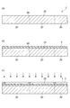
図1、2及び3は、半導体装置の製造方法の一実施形態を示す端面図である。本実施形態に係る半導体装置の製造方法は、半導体ウェハ2の回路面25に感光性接着剤からなるダイボンディングフィルム1を設ける工程(図1(a)、(b))と、露光及び現像により、ダイボンディングフィルム1を半導体ウェハ2のダイシングライン90が露出する開口11が形成されるようにパターニングする工程(図1(c)、図2(a))と、半導体ウェハ2を回路面25とは反対側からの研磨により薄くする工程(図2(b))と、露出したダイシングライン90に沿って半導体ウェハ2をダイシングブレード70によって切断することにより、半導体ウェハ2を複数の半導体チップ20に切り分ける工程(図2(c)、図3(a))とを備える。
1, 2 and 3 are end views showing one embodiment of a method of manufacturing a semiconductor device. The manufacturing method of the semiconductor device according to the present embodiment includes a step of providing a
図1(a)に示される半導体ウェハ2内には、ダイシングライン90によって区分された領域ごとに半導体チップ20が形成されている。この半導体チップ20の回路面25側の面に感光性接着剤からなるダイボンディングフィルム1が設けられる(図1(b))。予めフィルム状に成形された感光性接着剤を準備し、これをダイボンディングフィルム1として用いて半導体ウェハ2に貼り付ける方法が簡便である。
In the
ダイボンディングフィルム1を構成する感光性接着剤は、露光及び現像によってパターニングされた後に被着体に対する接着性を有し、アルカリ現像が可能なネガ型の感光性樹脂である。より詳細には、ダイボンディングフィルム1を露光及び現像によってパターニングして形成されるレジストパターンが、半導体チップ及びガラス基板等の被着体に対する接着性を有している。例えばレジストパターンに被着体を必要により加熱しながら圧着することにより、レジストパターンと被着体とを接着することが可能である。係る機能を有するダイボンディングフィルムに付与するための感光性接着剤の詳細については後述する。
The photosensitive adhesive constituting the
半導体ウェハ2に積層されたダイボンディングフィルム1に対して、所定の位置に開口を形成しているマスク3を介して活性光線(典型的には紫外線)を照射する(図1(c))。これによりダイボンディングフィルム1が所定のパターンで露光される。
The die
露光後、ダイボンディングフィルム1のうち露光されなかった部分をアルカリ現像液を用いた現像によって除去することにより、開口11が形成されるようにパターニングされる(図3(b))。開口11において半導体ウェハ2のダイシングライン90が露出する。なお、ネガ型に代えてポジ型の感光性接着剤を用いることも可能であり、その場合はダイボンディングフィルムのうち露光された部分が現像により除去される。
After the exposure, the unbonded portion of the
パターニングの後、半導体ウェハ2の感光性接着剤1とは反対側の面を研磨して、半導体ウェハ2を所定の厚さまで薄くする(図2(b))。研磨は、例えば、ダイボンディングフィルム1上に粘着フィルムを貼り付け、粘着フィルムによって半導体ウェハ2を研磨用の治具に固定して行われる。研磨の方法は、当該技術分野において通常用いられている機械研磨等の方法を採用することができる。
After the patterning, the surface of the semiconductor wafer 2 opposite to the
研磨後、半導体ウェハ2のダイボンディングフィルム1とは反対側の面にダイシングフィルム40を貼り付け、開口11において露出するダイシングライン90に沿って半導体ウェハ2をその回路面側から切断する(図2(c))。このダイシングにより、半導体ウェハ2が複数の半導体チップ20に切り分けられる(図3(a))。ダイシングは、例えば、ダイシングフィルム40によって全体をフレームに固定した状態で行われる。
After polishing, the
ダイシングの後、半導体チップ20がその回路面に貼り付けられたダイボンディングフィルム1とともにピックアップされる(図5(b))。ピックアップされた半導体チップ20は、半導体用の支持基材、又は他の半導体チップに対してダイボンディングフィルム1を介して接着される。その後、ワイヤボンディング、樹脂封止等の工程を経て半導体装置が得られる。
After the dicing, the
半導体チップ20の接着は、例えば、ダイボンディングフィルム1が流動性を発現するような温度にまで加熱しながら熱圧着する方法により行われる。熱圧着後、必要によりダイボンディングフィルム1を加熱して更に硬化を進行させる。
The bonding of the
以下、上記実施形態係る半導体装置の製造方法において用いられるダイボンディングフィルムを構成する感光性接着剤の好適な実施形態に関して説明する。 Hereinafter, a preferred embodiment of a photosensitive adhesive constituting a die bonding film used in the method for manufacturing a semiconductor device according to the embodiment will be described.
本実施形態に係る感光性接着剤は、アルカリ可溶性ポリマーと、放射線重合性化合物と、光重合開始剤とを含有するネガ型の感光性樹脂である。 The photosensitive adhesive according to the present embodiment is a negative photosensitive resin containing an alkali-soluble polymer, a radiation polymerizable compound, and a photopolymerization initiator.
アルカリ可溶性ポリマーは、アルカリ現像液に可溶であればよく、テトラメチルアンモニウムハイドライド水溶液に可溶であることが好ましい。例えば、カルボキシル基及び/又はフェノール性水酸基を有するポリマーであれば、アルカリ現像液への良好な溶解性を有する場合が多い。 The alkali-soluble polymer may be soluble in an alkaline developer, and is preferably soluble in an aqueous tetramethylammonium hydride solution. For example, a polymer having a carboxyl group and / or a phenolic hydroxyl group often has good solubility in an alkaline developer.
アルカリ可溶性ポリマーがカルボキシル基を有している場合、その酸価は好ましくは80〜180mg/KOHである。酸価が80〜180mg/KOHであることにより、アルカリ現像液によるパターン形成性、及び露光後の再接着性が特に良好になる。アルカリ可溶性ポリマーの酸価が80mg/KOH未満であるとアルカリ現像液への溶解性が低下する傾向があり、180mg/KOHを超えると現像中に感光性接着剤が被着体からはく離してしまう可能性が高くなる。同様の観点から、アルカリ可溶性ポリマーの酸価は150mg/KOH以下であることがより好ましい。特に、感光性接着剤が後述する熱硬化性樹脂を含有し、且つ、アルカリ可溶性ポリマーの酸価が80〜180mg/KOHであることが好ましい。 When the alkali-soluble polymer has a carboxyl group, the acid value is preferably 80 to 180 mg / KOH. When the acid value is 80 to 180 mg / KOH, the pattern formability with an alkali developer and the re-adhesion after exposure are particularly good. If the acid value of the alkali-soluble polymer is less than 80 mg / KOH, the solubility in an alkali developer tends to decrease, and if it exceeds 180 mg / KOH, the photosensitive adhesive peels off from the adherend during development. The possibility increases. From the same viewpoint, the acid value of the alkali-soluble polymer is more preferably 150 mg / KOH or less. In particular, it is preferable that the photosensitive adhesive contains a thermosetting resin described later, and the acid value of the alkali-soluble polymer is 80 to 180 mg / KOH.
露光後の良好な接着性を確保するために、アルカリ可溶性ポリマーのガラス転移温度(Tg)は、30〜150℃であることが好ましい。アルカリ可溶性ポリマーのTgが30℃未満であると、露光後の熱圧着時にボイドが生成しやすくなる傾向にある。Tgが150℃を超えると、露光前の被着体への貼付け温度及び露光後の圧着温度が高くなり周辺部材にダメージを与えやすくなる傾向にある。なお、上記Tgは粘弾性測定装置(レオメトリック社製)を用いてフィルム状の感光性接着剤の粘弾性の温度変化を測定したときのtanδのピーク温度である。 In order to ensure good adhesion after exposure, the glass transition temperature (Tg) of the alkali-soluble polymer is preferably 30 to 150 ° C. If the Tg of the alkali-soluble polymer is less than 30 ° C., voids tend to be easily generated during thermocompression bonding after exposure. When Tg exceeds 150 ° C., the temperature for pasting to the adherend before exposure and the pressure-bonding temperature after exposure tend to increase, and the peripheral members tend to be damaged. The above Tg is the peak temperature of tan δ when the temperature change of the viscoelasticity of the film-like photosensitive adhesive is measured using a viscoelasticity measuring device (Rheometric).
アルカリ可溶性ポリマーの重量平均分子量は5000〜150000であることが好ましく、20000〜500000がより好ましく、30000〜40000が更に好ましい。アルカリ可溶性ポリマーの重量平均分子量が5000より小さいと感光性接着剤のフィルム形成性が低下する傾向にあり、150000を超えるとアルカリ現像液への溶解性が低下して、現像時間が長くなる傾向にある。アルカリ可溶性ポリマーの重量平均分子量を5000〜150000とすることにより、露光後の再接着のための加熱温度を低くすることができるという効果も得られる。なお、上記の重量平均分子量は、高速液体クロマトグラフィー(例えば、島津製作所製「C−R4A」(商品名))を用いて測定される標準ポリスチレン換算値である。 The weight average molecular weight of the alkali-soluble polymer is preferably from 5,000 to 150,000, more preferably from 20,000 to 500,000, still more preferably from 30,000 to 40,000. If the weight average molecular weight of the alkali-soluble polymer is less than 5,000, the film-forming property of the photosensitive adhesive tends to be lowered, and if it exceeds 150,000, the solubility in an alkali developer is lowered and the development time tends to be longer. is there. By setting the weight average molecular weight of the alkali-soluble polymer to 5000 to 150,000, an effect that the heating temperature for re-adhesion after exposure can be lowered is also obtained. In addition, said weight average molecular weight is a standard polystyrene conversion value measured using a high performance liquid chromatography (For example, "C-R4A" (brand name) by Shimadzu Corporation).
アルカリ可溶性ポリマーは、エチレン性不飽和基等の放射線重合性官能基を有していてもよい。この場合、アルカリ可溶性ポリマーは放射線重合性化合物としても機能する。放射線重合性化合物として、放射線重合性官能基を有するアルカリ可溶性ポリマーのみを用いてもよいし、係るアルカリ可溶性ポリマーと、これとは別の放射線重合性化合物とを組合わせて用いてもよい。 The alkali-soluble polymer may have a radiation polymerizable functional group such as an ethylenically unsaturated group. In this case, the alkali-soluble polymer also functions as a radiation polymerizable compound. As the radiation-polymerizable compound, only an alkali-soluble polymer having a radiation-polymerizable functional group may be used, or such an alkali-soluble polymer and another radiation-polymerizable compound may be used in combination.
アルカリ可溶性ポリマーは、ポリイミド、ポリアミドイミド、ポリアミド酸、ポリベンゾオキサゾール、アクリルポリマー、スチレン−マレイン酸共重合体、ノボラック樹脂及びポリノルボルネン樹脂からなる群より選ばれる少なくとも1種のポリマーを含むことが好ましい。こららの中でも、ポリイミド、ポリアミド、ポリベンゾオキサゾール及びアクリルポリマーが好ましい。 The alkali-soluble polymer preferably contains at least one polymer selected from the group consisting of polyimide, polyamideimide, polyamic acid, polybenzoxazole, acrylic polymer, styrene-maleic acid copolymer, novolac resin, and polynorbornene resin. . Among these, polyimide, polyamide, polybenzoxazole and acrylic polymer are preferable.
アルカリ可溶性ポリマーとして用いられるポリイミドは、主鎖中にイミド骨格を有する1種又は2種以上の重合体から構成される。ポリイミドはカルボキシル基及び/又はフェノール性水酸基を有することが好ましい。 The polyimide used as the alkali-soluble polymer is composed of one or more polymers having an imide skeleton in the main chain. The polyimide preferably has a carboxyl group and / or a phenolic hydroxyl group.
カルボキシル基を有するポリイミドは、テトラカルボン酸二無水物と、カルボキシル基及びアミノ基を有するジアミンとの反応により、得ることができる。フェノール性水酸基を有するポリイミドは、テトラカルボン酸二無水物と、フェノール性水酸基及びアミノ基を有するジアミンとの反応により、得ることができる。これら反応により、ポリイミドにはジアミンに由来するカリボキシル基又はフェノール性水酸基が導入される。ジアミンの種類及びその仕込み比、反応条件等を適宜調整することにより、ポリイミドの酸価を所望の範囲に制御することができる。 A polyimide having a carboxyl group can be obtained by a reaction between a tetracarboxylic dianhydride and a diamine having a carboxyl group and an amino group. A polyimide having a phenolic hydroxyl group can be obtained by a reaction between a tetracarboxylic dianhydride and a diamine having a phenolic hydroxyl group and an amino group. Through these reactions, a carboxyl group or a phenolic hydroxyl group derived from diamine is introduced into the polyimide. The acid value of the polyimide can be controlled within a desired range by appropriately adjusting the type of diamine, its charging ratio, reaction conditions, and the like.
テトラカルボン酸二無水物とジアミンとの反応(縮合反応)は、当業者には理解されるように、公知の方法により行うことができる。例えば、この反応においては、まず、有機溶媒中で、テトラカルボン酸二無水物とジアミンとを、等モル又はほぼ等モルの比率で、反応温度80℃以下、好ましくは0〜60℃で付加反応させる。各成分の添加順序は任意である。反応が進行するにつれ反応液の粘度が徐々に上昇し、ポリイミドの前駆体であるポリアミド酸が生成する。生成したポリアミド酸を50〜80℃の温度に加熱して解重合させることによって、その分子量を調整することもできる。生成したポリアミド酸を脱水閉環させることにより、ポリイミドが生成する。脱水閉環は、加熱による熱閉環法、又は脱水剤を使用する化学閉環法により行うことができる。 The reaction (condensation reaction) between tetracarboxylic dianhydride and diamine can be carried out by a known method, as will be understood by those skilled in the art. For example, in this reaction, first, tetracarboxylic dianhydride and diamine are added in an organic solvent in an equimolar or almost equimolar ratio at a reaction temperature of 80 ° C. or less, preferably 0 to 60 ° C. Let The order of adding each component is arbitrary. As the reaction proceeds, the viscosity of the reaction solution gradually increases, and polyamic acid, which is a polyimide precursor, is generated. The molecular weight can be adjusted by heating the produced polyamic acid to a temperature of 50 to 80 ° C. for depolymerization. A polyimide is produced by dehydrating and ring-closing the produced polyamic acid. The dehydration ring closure can be performed by a thermal ring closure method by heating or a chemical ring closure method using a dehydrating agent.
テトラカルボン酸二無水物とジアミンとの仕込み比に関して、より具体的には、テトラカルボン酸二無水物の合計量1.0molに対して、ジアミンの合計量を好ましくは0.5〜2.0mol、より好ましくは0.8〜1.0molの範囲内とする。ジアミンの比率が2.0molを超えると末端がアミノ基であるポリイミドオリゴマーが多く生成し、0.5molを下回ると末端がカルボキシル基であるポリイミドオリゴマーが多く生成する傾向にある。ポリイミドオリゴマーの量が多くなると、ポリイミドの重量平均分子量が低下して、感光性接着剤の耐熱性等の種々の特性の低下が生じ易くなる。上記仕込み比を調整することによって、ポリイミドの重量平均分子量を5000〜150000の範囲内となるように調製することができる。 More specifically, regarding the charging ratio of tetracarboxylic dianhydride and diamine, more specifically, the total amount of diamine is preferably 0.5 to 2.0 mol with respect to 1.0 mol of the total amount of tetracarboxylic dianhydride. More preferably, it is in the range of 0.8 to 1.0 mol. When the ratio of the diamine exceeds 2.0 mol, many polyimide oligomers having amino groups at the ends are produced, and when the proportion is less than 0.5 mol, many polyimide oligomers having carboxyl groups at the ends tend to be produced. When the amount of the polyimide oligomer is increased, the weight average molecular weight of the polyimide is lowered, and various characteristics such as heat resistance of the photosensitive adhesive are easily lowered. By adjusting the charging ratio, the weight average molecular weight of the polyimide can be adjusted to be in the range of 5000 to 150,000.
ポリイミドの合成に使用されるジアミンとしては、アルカリ現像液への溶解性を特に良好なものとするために、上述の式(I−a)、(I−b)、(II−a)、(II−b)又は(II−c)で表される芳香族ジアミンが好ましい。 As the diamine used for the synthesis of the polyimide, in order to particularly improve the solubility in an alkali developer, the above formulas (Ia), (Ib), (II-a), (II The aromatic diamine represented by II-b) or (II-c) is preferable.
ポリイミドのTgを低下させて熱応力を低減するため、ジアミンは、更に、下記一般式(III)で表される脂肪族エーテルジアミンを含むことが好ましい。式(III)中、Q1、Q2及びQ3はそれぞれ独立に炭素数1〜10のアルキレン基を示し、n1は1〜80の整数を示す。 In order to reduce the Tg of polyimide and reduce thermal stress, the diamine preferably further contains an aliphatic ether diamine represented by the following general formula (III). In formula (III), Q 1 , Q 2 and Q 3 each independently represent an alkylene group having 1 to 10 carbon atoms, and n 1 represents an integer of 1 to 80.
式(III)の脂肪族エーテルジアミンとしては、より具体的には、下記化学式(IIIa)、(IIIb)又は(IIIc)で表されるものが挙げられる。これらの中でも、露光前の低温での貼付け性及び露光後の被着体に対する良好な接着性を確保できる点で、式(IIIa)の脂肪族エーテルジアミンが好ましい。 More specific examples of the aliphatic ether diamine of the formula (III) include those represented by the following chemical formula (IIIa), (IIIb) or (IIIc). Among these, the aliphatic ether diamine of the formula (IIIa) is preferable in that it can secure the adhesion at a low temperature before the exposure and the good adhesion to the adherend after the exposure.
脂肪族エーテルジアミンの市販品としては、例えば、サン テクノケミカル(株)製のジェファーミン「D−230」、「D−400」、「D−2000」、「D−4000」、「ED−600」、「ED−900」、「ED−2001」、「EDR−148」(以上商品名)、BASF(製)のポリエーテルアミン「D−230」、「D−400」、「D−2000」(以上商品名)が挙げられる。 Commercially available products of aliphatic ether diamines include, for example, Jeffamine “D-230”, “D-400”, “D-2000”, “D-4000”, “ED-600” manufactured by Sun Techno Chemical Co., Ltd. ”,“ ED-900 ”,“ ED-2001 ”,“ EDR-148 ”(trade name), BASF (manufactured) polyetheramine“ D-230 ”,“ D-400 ”,“ D-2000 ” (Product name).
更に、露光後の再接着性を更に高めるために、下記一般式(IV)で表されるシロキサンジアミンを使用することが好ましい。式(IV)中、R1及びR2はそれぞれ独立に炭素数1〜5のアルキレン基又は置換基を有してもよいフェニレン基を示し、R3、R4、R5及びR6はそれぞれ独立に炭素数1〜5のアルキル基、フェニル基又はフェノキシ基を示し、n2は1〜5の整数を示す。 Furthermore, in order to further improve the re-adhesion after exposure, it is preferable to use a siloxane diamine represented by the following general formula (IV). In formula (IV), R 1 and R 2 each independently represent an alkylene group having 1 to 5 carbon atoms or a phenylene group which may have a substituent, and R 3 , R 4 , R 5 and R 6 are each Independently, it represents an alkyl group having 1 to 5 carbon atoms, a phenyl group or a phenoxy group, and n 2 represents an integer of 1 to 5.
化学式(IV)で表されるシロキサンジアミンとしては、例えば、式中のn2が1のとき、1,1,3,3−テトラメチル−1,3−ビス(4−アミノフェニル)ジシロキサン、1,1,3,3−テトラフェノキシ−1,3−ビス(4−アミノエチル)ジシロキサン、1,1,3,3−テトラフェニル−1,3−ビス(2−アミノエチル)ジシロキサン、1,1,3,3−テトラフェニル−1,3−ビス(3−アミノプロピル)ジシロキサン、1,1,3,3−テトラメチル−1,3−ビス(2−アミノエチル)ジシロキサン、1,1,3,3−テトラメチル−1,3−ビス(3−アミノプロピル)ジシロキサン、1,1,3,3−テトラメチル−1,3−ビス(3−アミノブチル)ジシロキサン、1,3−ジメチル−1,3−ジメトキシ−1,3−ビス(4−アミノブチル)ジシロキサンが挙げられる。n2が2のとき、1,1,3,3,5,5−ヘキサメチル−1,5−ビス(4−アミノフェニル)トリシロキサン、1,1,5,5−テトラフェニル−3,3−ジメチル−1,5−ビス(3−アミノプロピル)トリシロキサン、1,1,5,5−テトラフェニル−3,3−ジメトキシ−1,5−ビス(4−アミノブチル)トリシロキサン、1,1,5,5−テトラフェニル−3,3−ジメトキシ−1,5−ビス(5−アミノペンチル)トリシロキサン、1,1,5,5−テトラメチル−3,3−ジメトキシ−1,5−ビス(2−アミノエチル)トリシロキサン、1,1,5,5−テトラメチル−3,3−ジメトキシ−1,5−ビス(4−アミノブチル)トリシロキサン、1,1,5,5−テトラメチル−3,3−ジメトキシ−1,5−ビス(5−アミノペンチル)トリシロキサン、1,1,3,3,5,5−ヘキサメチル−1,5−ビス(3−アミノプロピル)トリシロキサン、1,1,3,3,5,5−ヘキサエチル−1,5−ビス(3−アミノプロピル)トリシロキサン、1,1,3,3,5,5−ヘキサプロピル−1,5−ビス(3−アミノプロピル)トリシロキサンが挙げられる。 As the siloxane diamine represented by the chemical formula (IV), for example, when n 2 in the formula is 1, 1,1,3,3-tetramethyl-1,3-bis (4-aminophenyl) disiloxane, 1,1,3,3-tetraphenoxy-1,3-bis (4-aminoethyl) disiloxane, 1,1,3,3-tetraphenyl-1,3-bis (2-aminoethyl) disiloxane, 1,1,3,3-tetraphenyl-1,3-bis (3-aminopropyl) disiloxane, 1,1,3,3-tetramethyl-1,3-bis (2-aminoethyl) disiloxane, 1,1,3,3-tetramethyl-1,3-bis (3-aminopropyl) disiloxane, 1,1,3,3-tetramethyl-1,3-bis (3-aminobutyl) disiloxane, 1,3-dimethyl-1,3-dimethoxy- 1,3-bis (4-aminobutyl) disiloxane may be mentioned. When n 2 is 2, 1,1,3,3,5,5-hexamethyl-1,5-bis (4-aminophenyl) trisiloxane, 1,1,5,5-tetraphenyl-3,3- Dimethyl-1,5-bis (3-aminopropyl) trisiloxane, 1,1,5,5-tetraphenyl-3,3-dimethoxy-1,5-bis (4-aminobutyl) trisiloxane, 1,1 , 5,5-tetraphenyl-3,3-dimethoxy-1,5-bis (5-aminopentyl) trisiloxane, 1,1,5,5-tetramethyl-3,3-dimethoxy-1,5-bis (2-aminoethyl) trisiloxane, 1,1,5,5-tetramethyl-3,3-dimethoxy-1,5-bis (4-aminobutyl) trisiloxane, 1,1,5,5-tetramethyl −3,3-dimethoxy-1,5-bis ( 5-aminopentyl) trisiloxane, 1,1,3,3,5,5-hexamethyl-1,5-bis (3-aminopropyl) trisiloxane, 1,1,3,3,5,5-hexaethyl- Examples include 1,5-bis (3-aminopropyl) trisiloxane and 1,1,3,3,5,5-hexapropyl-1,5-bis (3-aminopropyl) trisiloxane.
これらのジアミンは単独で、又は2種以上を組み合わせて使用することができる。例えば、式(Ia)、(Ib)、(II−a)、(II−b)又は(II−c)で表される芳香族ジアミンを全ジアミンの10〜50モル%、一般式(IV)で表されるシロキサンジアミンを全ジアミンの1〜20モル%(更に好ましくは5〜10モル%)、一般式(III)で表される脂肪族エーテルジアミンを全ジアミンの10〜90モル%とすることが好ましい。式(Ia)又は(Ib)で表される芳香族ジアミンを上記比率で用いることにより、通常、ポリイミドの酸価を80〜180mg/KOH又は80〜150mg/KOHとすることができる。シロキサンジアミンが全ジアミンの1モル%未満であると、露光後の再接着性が低下する傾向にあり、20モル%を超えるとアルカリ現像液への溶解性が低下する傾向にある。また、脂肪族エーテルジアミンが全ジアミンの10モル%未満であると、ポリイミドのTgが高くなって低温加工性(低温での貼付け性)が低下する傾向にあり、90モル%を超えると、露光後の熱圧着時にボイドが発生しやすくなる傾向にある。 These diamines can be used alone or in combination of two or more. For example, the aromatic diamine represented by the formula (Ia), (Ib), (II-a), (II-b) or (II-c) is added in an amount of 10 to 50 mol% of the total diamine, and the general formula (IV) 1 to 20 mol% (more preferably 5 to 10 mol%) of the total diamine, and the aliphatic ether diamine represented by the general formula (III) is 10 to 90 mol% of the total diamine. It is preferable. By using the aromatic diamine represented by the formula (Ia) or (Ib) at the above ratio, the acid value of the polyimide can be usually 80 to 180 mg / KOH or 80 to 150 mg / KOH. When the siloxane diamine is less than 1 mol% of the total diamine, the re-adhesion property after exposure tends to decrease, and when it exceeds 20 mol%, the solubility in an alkali developer tends to decrease. If the aliphatic ether diamine is less than 10 mol% of the total diamine, the Tg of the polyimide tends to be high and the low-temperature processability (sticking property at low temperature) tends to decrease. Voids tend to be easily generated during subsequent thermocompression bonding.
ジアミンは、上記以外のジアミンを更に含んでいてもよい。例えば、o−フェニレンジアミン、m−フェニレンジアミン、p−フェニレンジアミン、3,3’−ジアミノジフェニルエーテル、3,4’−ジアミノジフェニルエーテル、4,4’−ジアミノジフェニルエーテル、3,3’−ジアミノジフェニルメタン、3,4’−ジアミノジフェニルメタン、4,4’−ジアミノジフェニルエーテメタン、ビス(4−アミノ−3,5−ジメチルフェニル)メタン、ビス(4−アミノ−3,5−ジイソプロピルフェニル)メタン、3,3’−ジアミノジフェニルジフルオロメタン、3,4’−ジアミノジフェニルジフルオロメタン、4,4’−ジアミノジフェニルジフルオロメタン、3,3’−ジアミノジフェニルスルフォン、3,4’−ジアミノジフェニルスルフォン、4,4’−ジアミノジフェニルスルフォン、3,3’−ジアミノジフェニルスルフィド、3,4’−ジアミノジフェニルスルフィド、4,4’−ジアミノジフェニルスルフィド、3,3’−ジアミノジフェニルケトン、3,4’−ジアミノジフェニルケトン、4,4’−ジアミノジフェニルケトン、2,2−ビス(3−アミノフェニル)プロパン、2,2’−(3,4’−ジアミノジフェニル)プロパン、2,2−ビス(4−アミノフェニル)プロパン、2,2−ビス(3−アミノフェニル)ヘキサフルオロプロパン、2,2−(3,4’−ジアミノジフェニル)ヘキサフルオロプロパン、2,2−ビス(4−アミノフェニル)ヘキサフルオロプロパン、1,3−ビス(3−アミノフェノキシ)ベンゼン、1,4−ビス(3−アミノフェノキシ)ベンゼン、1,4−ビス(4−アミノフェノキシ)ベンゼン、3,3’−(1,4−フェニレンビス(1−メチルエチリデン))ビスアニリン、3,4’−(1,4−フェニレンビス(1−メチルエチリデン))ビスアニリン、4,4’−(1,4−フェニレンビス(1−メチルエチリデン))ビスアニリン、2,2−ビス(4−(3−アミノフェノキシ)フェニル)プロパン、2,2−ビス(4−(3−アミノフェノキシ)フェニル)ヘキサフルオロプロパン、2,2−ビス(4−(4−アミノフェノキシ)フェニル)ヘキサフルオロプロパン、ビス(4−(3−アミノエノキシ)フェニル)スルフィド、ビス(4−(4−アミノエノキシ)フェニル)スルフィド、ビス(4−(3−アミノエノキシ)フェニル)スルフォン、ビス(4−(4−アミノエノキシ)フェニル)スルフォン、1,3−ビス(アミノメチル)シクロヘキサン及び2,2−ビス(4−アミノフェノキシフェニル)プロパンが挙げられる。 The diamine may further contain a diamine other than those described above. For example, o-phenylenediamine, m-phenylenediamine, p-phenylenediamine, 3,3′-diaminodiphenyl ether, 3,4′-diaminodiphenyl ether, 4,4′-diaminodiphenyl ether, 3,3′-diaminodiphenylmethane, 3 , 4′-diaminodiphenylmethane, 4,4′-diaminodiphenylethermethane, bis (4-amino-3,5-dimethylphenyl) methane, bis (4-amino-3,5-diisopropylphenyl) methane, 3,3 ′ -Diaminodiphenyldifluoromethane, 3,4'-diaminodiphenyldifluoromethane, 4,4'-diaminodiphenyldifluoromethane, 3,3'-diaminodiphenylsulfone, 3,4'-diaminodiphenylsulfone, 4,4'-diamino Diphenyls Phon, 3,3′-diaminodiphenyl sulfide, 3,4′-diaminodiphenyl sulfide, 4,4′-diaminodiphenyl sulfide, 3,3′-diaminodiphenyl ketone, 3,4′-diaminodiphenyl ketone, 4,4 '-Diaminodiphenyl ketone, 2,2-bis (3-aminophenyl) propane, 2,2'-(3,4'-diaminodiphenyl) propane, 2,2-bis (4-aminophenyl) propane, 2, 2-bis (3-aminophenyl) hexafluoropropane, 2,2- (3,4'-diaminodiphenyl) hexafluoropropane, 2,2-bis (4-aminophenyl) hexafluoropropane, 1,3-bis (3-aminophenoxy) benzene, 1,4-bis (3-aminophenoxy) benzene, 1,4-bis (4 Aminophenoxy) benzene, 3,3 ′-(1,4-phenylenebis (1-methylethylidene)) bisaniline, 3,4 ′-(1,4-phenylenebis (1-methylethylidene)) bisaniline, 4,4 '-(1,4-phenylenebis (1-methylethylidene)) bisaniline, 2,2-bis (4- (3-aminophenoxy) phenyl) propane, 2,2-bis (4- (3-aminophenoxy) Phenyl) hexafluoropropane, 2,2-bis (4- (4-aminophenoxy) phenyl) hexafluoropropane, bis (4- (3-aminoenoxy) phenyl) sulfide, bis (4- (4-aminoenoxy) phenyl) Sulfide, bis (4- (3-aminoenoxy) phenyl) sulfone, bis (4- (4-aminoenoxy) phenyl ) Sulfone, 1,3-bis (aminomethyl) cyclohexane and 2,2-bis (4-aminophenoxyphenyl) propane.
ポリイミドを合成する際の原料として用いるテトラカルボン酸二無水物は、接着剤の諸特性の低下を抑えるため、無水酢酸からの再結晶により精製されていることが好ましい。あるいは、テトラカルボン酸二無水物は、その融点よりも10〜20℃低い温度で12時間以上加熱することにより乾燥されていてもよい。テトラカルボン酸二無水物の純度は、示差走査熱量計(DSC)によって測定される吸熱開始温度と吸熱ピーク温度との差によって評価することができ、再結晶や乾燥等によりこの差が20℃以内、より好ましくは10℃以内となるように精製されたカルボン酸二無水物をポリイミドの合成のために用いることが好ましい。吸熱開始温度及び吸熱ピーク温度は、DSC(パーキンエルマー社製DSC−7型)を用いて、サンプル量:5mg、昇温速度:5℃/min、測定雰囲気:窒素の条件で測定される。 Tetracarboxylic dianhydride used as a raw material for the synthesis of polyimide is preferably purified by recrystallization from acetic anhydride in order to suppress deterioration of various properties of the adhesive. Alternatively, the tetracarboxylic dianhydride may be dried by heating at a temperature lower by 10 to 20 ° C. than its melting point for 12 hours or more. The purity of tetracarboxylic dianhydride can be evaluated by the difference between the endothermic onset temperature measured by a differential scanning calorimeter (DSC) and the endothermic peak temperature, and this difference is within 20 ° C. due to recrystallization or drying. More preferably, carboxylic dianhydride purified so as to be within 10 ° C. is used for the synthesis of polyimide. The endothermic start temperature and endothermic peak temperature are measured using DSC (DSC-7, manufactured by Perkin Elmer Co.) under the conditions of sample amount: 5 mg, temperature increase rate: 5 ° C./min, measurement atmosphere: nitrogen.
テトラカルボン酸二無水物としては、例えば、ピロメリット酸二無水物、3,3’,4,4’−ビフェニルテトラカルボン酸二無水物、2,2’,3,3’−ビフェニルテトラカルボン酸二無水物、2,2−ビス(3,4−ジカルボキシフェニル)プロパン二無水物、2,2−ビス(2,3−ジカルボキシフェニル)プロパン二無水物、1,1−ビス(2,3−ジカルボキシフェニル)エタン二無水物、1,1−ビス(3,4−ジカルボキシフェニル)エタン二無水物、ビス(2,3−ジカルボキシフェニル)メタン二無水物、ビス(3,4−ジカルボキシフェニル)メタン二無水物、ビス(3,4−ジカルボキシフェニル)スルホン二無水物、3,4,9,10−ペリレンテトラカルボン酸二無水物、ビス(3,4−ジカルボキシフェニル)エーテル二無水物、ベンゼン−1,2,3,4−テトラカルボン酸二無水物、3,4,3’,4’−ベンゾフェノンテトラカルボン酸二無水物、2,3,2’,3’−ベンゾフェノンテトラカルボン酸二無水物、3,3,3’,4’−ベンゾフェノンテトラカルボン酸二無水物、1,2,5,6−ナフタレンテトラカルボン酸二無水物、1,4,5,8−ナフタレンテトラカルボン酸二無水物、2,3,6,7−ナフタレンテトラカルボン酸二無水物、1,2,4,5−ナフタレンテトラカルボン酸二無水物、2,6−ジクロロナフタレン−1,4,5,8−テトラカルボン酸二無水物、2,7−ジクロロナフタレン−1,4,5,8−テトラカルボン酸二無水物、2,3,6,7−テトラクロロナフタレン−1,4,5,8−テトラカルボン酸二無水物、フェナンスレン−1,8,9,10−テトラカルボン酸二無水物、ピラジン−2,3,5,6−テトラカルボン酸二無水物、チオフェン−2,3,5,6−テトラカルボン酸二無水物、2,3,3’,4’−ビフェニルテトラカルボン酸二無水物、3,4,3’,4’−ビフェニルテトラカルボン酸二無水物、2,3,2’,3’−ビフェニルテトラカルボン酸二無水物、ビス(3,4−ジカルボキシフェニル)ジメチルシラン二無水物、ビス(3,4−ジカルボキシフェニル)メチルフェニルシラン二無水物、ビス(3,4−ジカルボキシフェニル)ジフェニルシラン二無水物、1,4−ビス(3,4−ジカルボキシフェニルジメチルシリル)ベンゼン二無水物、1,3−ビス(3,4−ジカルボキシフェニル)−1,1,3,3−テトラメチルジシクロヘキサン二無水物、p−フェニレンビス(トリメリテート無水物)、エチレンテトラカルボン酸二無水物、1,2,3,4−ブタンテトラカルボン酸二無水物、デカヒドロナフタレン−1,4,5,8−テトラカルボン酸二無水物、4,8−ジメチル−1,2,3,5,6,7−ヘキサヒドロナフタレン−1,2,5,6−テトラカルボン酸二無水物、シクロペンタン−1,2,3,4−テトラカルボン酸二無水物、ピロリジン−2,3,4,5−テトラカルボン酸二無水物、1,2,3,4−シクロブタンテトラカルボン酸二無水物、ビス(エキソ−ビシクロ[2,2,1]ヘプタン−2,3−ジカルボン酸二無水物、ビシクロ−[2,2,2]−オクト−7−エン−2,3,5,6−テトラカルボン酸二無水物、2,2−ビス(3,4−ジカルボキシフェニル)プロパン二無水物、2,2−ビス[4−(3,4−ジカルボキシフェニル)フェニル]プロパン二無水物、2,2−ビス(3,4−ジカルボキシフェニル)ヘキサフルオロプロパン二無水物、2,2−ビス[4−(3,4−ジカルボキシフェニル)フェニル]ヘキサフルオロプロパン二無水物、4,4’−ビス(3,4−ジカルボキシフェノキシ)ジフェニルスルフィド二無水物、1,4−ビス(2−ヒドロキシヘキサフルオロイソプロピル)ベンゼンビス(トリメリット酸無水物)、1,3−ビス(2−ヒドロキシヘキサフルオロイソプロピル)ベンゼンビス(トリメリット酸無水物)、5−(2,5−ジオキソテトラヒドロフリル)−3−メチル−3−シクロヘキセン−1,2−ジカルボン酸二無水物、及びテトラヒドロフラン−2,3,4,5−テトラカルボン酸二無水物が挙げられる。 Examples of the tetracarboxylic dianhydride include pyromellitic dianhydride, 3,3 ′, 4,4′-biphenyltetracarboxylic dianhydride, and 2,2 ′, 3,3′-biphenyltetracarboxylic acid. Dianhydride, 2,2-bis (3,4-dicarboxyphenyl) propane dianhydride, 2,2-bis (2,3-dicarboxyphenyl) propane dianhydride, 1,1-bis (2, 3-dicarboxyphenyl) ethane dianhydride, 1,1-bis (3,4-dicarboxyphenyl) ethane dianhydride, bis (2,3-dicarboxyphenyl) methane dianhydride, bis (3,4 -Dicarboxyphenyl) methane dianhydride, bis (3,4-dicarboxyphenyl) sulfone dianhydride, 3,4,9,10-perylenetetracarboxylic dianhydride, bis (3,4-dicarboxyphenyl) Ether dianhydride, benzene-1,2,3,4-tetracarboxylic dianhydride, 3,4,3 ′, 4′-benzophenone tetracarboxylic dianhydride, 2,3,2 ′, 3′- Benzophenone tetracarboxylic dianhydride, 3,3,3 ′, 4′-benzophenone tetracarboxylic dianhydride, 1,2,5,6-naphthalene tetracarboxylic dianhydride, 1,4,5,8- Naphthalenetetracarboxylic dianhydride, 2,3,6,7-naphthalenetetracarboxylic dianhydride, 1,2,4,5-naphthalenetetracarboxylic dianhydride, 2,6-dichloronaphthalene-1,4 , 5,8-tetracarboxylic dianhydride, 2,7-dichloronaphthalene-1,4,5,8-tetracarboxylic dianhydride, 2,3,6,7-tetrachloronaphthalene-1,4 5,8-Tetracar Acid dianhydride, phenanthrene-1,8,9,10-tetracarboxylic dianhydride, pyrazine-2,3,5,6-tetracarboxylic dianhydride, thiophene-2,3,5,6- Tetracarboxylic dianhydride, 2,3,3 ′, 4′-biphenyltetracarboxylic dianhydride, 3,4,3 ′, 4′-biphenyltetracarboxylic dianhydride, 2,3,2 ′, 3′-biphenyltetracarboxylic dianhydride, bis (3,4-dicarboxyphenyl) dimethylsilane dianhydride, bis (3,4-dicarboxyphenyl) methylphenylsilane dianhydride, bis (3,4- Dicarboxyphenyl) diphenylsilane dianhydride, 1,4-bis (3,4-dicarboxyphenyldimethylsilyl) benzene dianhydride, 1,3-bis (3,4-dicarboxyphenyl) -1,1, 3,3-tetramethyldicyclohexane dianhydride, p-phenylenebis (trimellitic anhydride), ethylenetetracarboxylic dianhydride, 1,2,3,4-butanetetracarboxylic dianhydride, decahydronaphthalene- 1,4,5,8-tetracarboxylic dianhydride, 4,8-dimethyl-1,2,3,5,6,7-hexahydronaphthalene-1,2,5,6-tetracarboxylic dianhydride , Cyclopentane-1,2,3,4-tetracarboxylic dianhydride, pyrrolidine-2,3,4,5-tetracarboxylic dianhydride, 1,2,3,4-cyclobutanetetracarboxylic dianhydride Anhydride, bis (exo-bicyclo [2,2,1] heptane-2,3-dicarboxylic dianhydride, bicyclo- [2,2,2] -oct-7-ene-2,3,5,6 -Tetracarboxylic acid 2,2-bis (3,4-dicarboxyphenyl) propane dianhydride, 2,2-bis [4- (3,4-dicarboxyphenyl) phenyl] propane dianhydride, 2,2-bis (3,4-dicarboxyphenyl) hexafluoropropane dianhydride, 2,2-bis [4- (3,4-dicarboxyphenyl) phenyl] hexafluoropropane dianhydride, 4,4′-bis (3 , 4-Dicarboxyphenoxy) diphenyl sulfide dianhydride, 1,4-bis (2-hydroxyhexafluoroisopropyl) benzene bis (trimellitic anhydride), 1,3-bis (2-hydroxyhexafluoroisopropyl) benzene Bis (trimellitic anhydride), 5- (2,5-dioxotetrahydrofuryl) -3-methyl-3-cyclohexene-1,2-di Carboxylic acid dianhydride, and tetrahydrofuran-2,3,4,5-tetracarboxylic acid dianhydride.
特に、溶剤への良好な溶解性を付与するため、下記化学式(V)又は(VI)で表されるテトラカルボン酸二無水物が好ましい。この場合、これらの式で表されるテトラカルボン酸二無水物の割合を、全テトラカルボン酸二無水物100モル%に対して50モル%以上とすることが好ましい。この割合が50モル%未満であると、溶解性向上効果が低下する傾向にある。 In particular, a tetracarboxylic dianhydride represented by the following chemical formula (V) or (VI) is preferable in order to impart good solubility in a solvent. In this case, it is preferable that the ratio of the tetracarboxylic dianhydrides represented by these formulas be 50 mol% or more with respect to 100 mol% of all tetracarboxylic dianhydrides. When this proportion is less than 50 mol%, the effect of improving solubility tends to be reduced.
以上のようなテトラカルボン酸二無水物は、単独で又は二種類以上を組み合わせて使用することができる。 The above tetracarboxylic dianhydrides can be used alone or in combination of two or more.
放射線重合性化合物は、紫外線や電子ビームなどの放射線の照射により、重合する化合物である。放射線重合性化合物は、アクリート基及びメタクリレート基のようなエチレン性不飽和基を有する化合物であることが好ましい。放射線重合性化合物の具体例としては、アクリル酸メチル、メタクリル酸メチル、アクリル酸エチル、メタクリル酸エチル、アクリル酸ブチル、メタクリル酸ブチル、アクリル酸2−エチルヘキシル、メタクリル酸2−エチルヘキシル、ペンテニルアクリレート、テトラヒドロフルフリルアクリレート、テトラヒドロフルフリルメタクリレート、ジエチレングリコールジアクリレート、トリエチレングリコールジアクリレート、テトラエチレングリコールジアクリレート、ジエチレングリコールジメタクリレート、トリエチレングリコールジメタクリレート、テトラエチレングリコールジメタクリレート、トリメチロールプロパンジアクリレート、トリメチロールプロパントリアクリレート、トリメチロールプロパンジメタクリレート、トリメチロールプロパントリメタクリレート、1,4−ブタンジオールジアクリレート、1,6−ヘキサンジオールジアクリレート、1,4−ブタンジオールジメタクリレート、1,6−ヘキサンジオールジメタクリレート、ペンタエリスリトールトリアクリレート、ペンタエリスリトールテトラアクリレート、ペンタエリスリトールトリメタクリレート、ペンタエリスリトールテトラメタクリレート、ジペンタエリスリトールヘキサアクリレート、ジペンタエリスリトールヘキサメタクリレート、スチレン、ジビニルベンゼン、4−ビニルトルエン、4−ビニルピリジン、N−ビニルピロリドン、2−ヒドロキシエチルアクリレート、2−ヒドロキシエチルメタクリレート、1,3−アクリロイルオキシ−2−ヒドロキシプロパン、1,2−メタクリロイルオキシ−2−ヒドロキシプロパン、メチレンビスアクリルアミド、N,N−ジメチルアクリルアミド、N−メチロールアクリルアミド、トリス(β−ヒドロキシエチル)イソシアヌレートのトリアクリレート、下記一般式(10)で表される化合物、ウレタンアクリレート若しくはウレタンメタクリレート、及び尿素アクリレートが挙げられる。式(10)中、R3及びR4はそれぞれ独立に水素原子又はメチル基を示し、q及びrはそれぞれ独立に1以上の整数を示す。 A radiation-polymerizable compound is a compound that polymerizes upon irradiation with radiation such as ultraviolet rays or electron beams. The radiation polymerizable compound is preferably a compound having an ethylenically unsaturated group such as an acrylate group and a methacrylate group. Specific examples of the radiation polymerizable compound include methyl acrylate, methyl methacrylate, ethyl acrylate, ethyl methacrylate, butyl acrylate, butyl methacrylate, 2-ethylhexyl acrylate, 2-ethylhexyl methacrylate, pentenyl acrylate, tetrahydro Furfuryl acrylate, tetrahydrofurfuryl methacrylate, diethylene glycol diacrylate, triethylene glycol diacrylate, tetraethylene glycol diacrylate, diethylene glycol dimethacrylate, triethylene glycol dimethacrylate, tetraethylene glycol dimethacrylate, trimethylolpropane diacrylate, trimethylolpropane Triacrylate, trimethylolpropane dimethacrylate, tri Tyrolpropane trimethacrylate, 1,4-butanediol diacrylate, 1,6-hexanediol diacrylate, 1,4-butanediol dimethacrylate, 1,6-hexanediol dimethacrylate, pentaerythritol triacrylate, pentaerythritol tetraacrylate , Pentaerythritol trimethacrylate, pentaerythritol tetramethacrylate, dipentaerythritol hexaacrylate, dipentaerythritol hexamethacrylate, styrene, divinylbenzene, 4-vinyltoluene, 4-vinylpyridine, N-vinylpyrrolidone, 2-hydroxyethyl acrylate, 2 -Hydroxyethyl methacrylate, 1,3-acryloyloxy-2-hydroxypropane, 1,2-methan Acryloyloxy-2-hydroxypropane, methylenebisacrylamide, N, N-dimethylacrylamide, N-methylolacrylamide, triacrylate of tris (β-hydroxyethyl) isocyanurate, a compound represented by the following general formula (10), Examples include urethane acrylate or urethane methacrylate, and urea acrylate. In formula (10), R 3 and R 4 each independently represent a hydrogen atom or a methyl group, and q and r each independently represent an integer of 1 or more.
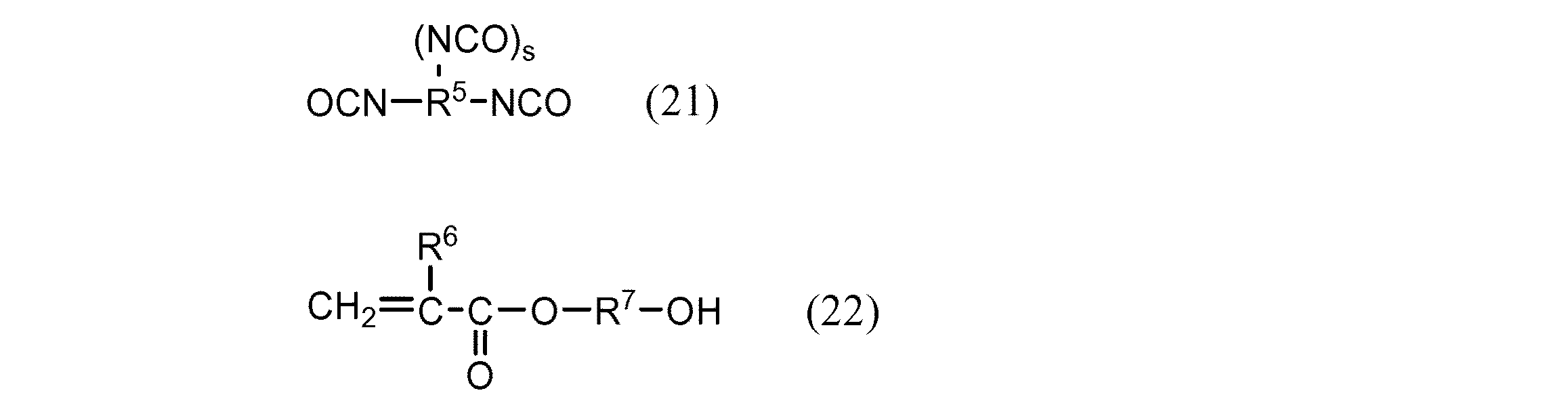
ウレタンアクリレート及びウレタンメタクリレートは、例えば、ジオール類、下記一般式(21)で表されるイソシアネート化合物、及び下記一般式(22)で表される化合物の反応により生成する。 Urethane acrylate and urethane methacrylate are produced, for example, by a reaction of a diol, an isocyanate compound represented by the following general formula (21), and a compound represented by the following general formula (22).
式(21)中、sは0又は1を示し、R5は炭素原子数が1〜30の2価又は3価の有機基を示す。式(22)中、R6は水素原子又はメチル基を示し、R7はエチレン基又はプロピレン基を示す。 In the formula (21), s represents 0 or 1, and R 5 represents a divalent or trivalent organic group having 1 to 30 carbon atoms. In formula (22), R 6 represents a hydrogen atom or a methyl group, and R 7 represents an ethylene group or a propylene group.
尿素メタクリレートは、例えば、下記一般式(31)で表されるジアミンと、下記一般式(32)で表される化合物との反応により生成する。 Urea methacrylate is produced, for example, by a reaction between a diamine represented by the following general formula (31) and a compound represented by the following general formula (32).
式(31)中、R8は炭素原子数が2〜30の2価の有機基を示す。式(32)中、tは0又は1を示す。 In formula (31), R 8 represents a divalent organic group having 2 to 30 carbon atoms. In formula (32), t represents 0 or 1.
以上のような化合物の他、官能基を含むビニル共重合体に、少なくとも1個のエチレン性不飽和基と、オキシラン環、イソシアネート基、水酸基、及びカルボキシル基等の官能基とを有する化合物を付加反応させて得られる、側鎖にエチレン性不飽和基を有する放射線重合性共重合体等などを使用することができる。 In addition to the above compounds, a compound having at least one ethylenically unsaturated group and a functional group such as an oxirane ring, an isocyanate group, a hydroxyl group, and a carboxyl group is added to a vinyl copolymer containing a functional group. A radiation-polymerizable copolymer having an ethylenically unsaturated group in the side chain and the like obtained by the reaction can be used.
これらの放射線重合性化合物は、単独で又は2種類以上を組み合わせて使用することができる。なかでも上記一般式(10)で示される放射線重合性化合物は硬化後の耐溶剤性を付与できる点で好ましく、ウレタンアクリレート及びウレタンメタクリレートは硬化後の可とう性を付与できる点で好ましい。 These radiation polymerizable compounds can be used alone or in combination of two or more. Among these, the radiation polymerizable compound represented by the general formula (10) is preferable in that it can provide solvent resistance after curing, and urethane acrylate and urethane methacrylate are preferable in that they can provide flexibility after curing.
放射線重合性化合物の分子量は2000以下が好ましい。分子量が2000を超えると、感光性接着剤のアルカリ現像液への溶解性が低下する傾向にあり、また、接着フィルムのタック性が低下して、半導体ウェハ等の被着体に低温で貼付けることが困難となる傾向にある。 The molecular weight of the radiation polymerizable compound is preferably 2000 or less. When the molecular weight exceeds 2000, the solubility of the photosensitive adhesive in an alkaline developer tends to be reduced, and the tackiness of the adhesive film is reduced, so that the adhesive is stuck to an adherend such as a semiconductor wafer at a low temperature. Tend to be difficult.
放射線重合性化合物の含有量は、アルカリ可溶性ポリマー100重量部に対して20〜80重量部であることが好ましく、30〜60重量部であることが更に好ましい。放射線重合性化合物の量が80重量部を超えると、重合した放射線重合性化合物が原因となって熱圧着後の接着性が低下する傾向にある。5重量部未満であると、露光後の耐溶剤性が低くなり、パターンを形成するのが困難となる傾向にある。 The content of the radiation-polymerizable compound is preferably 20 to 80 parts by weight, more preferably 30 to 60 parts by weight with respect to 100 parts by weight of the alkali-soluble polymer. When the amount of the radiation polymerizable compound exceeds 80 parts by weight, the adhesiveness after thermocompression bonding tends to decrease due to the polymerized radiation polymerizable compound. If it is less than 5 parts by weight, the solvent resistance after exposure tends to be low, and it tends to be difficult to form a pattern.
光重合開始剤は、パターン形成時の感度を良くするために、300〜400nmにおいて吸収帯を有することが好ましい。光重合開始剤の具体例としては、ベンゾフェノン、N,N’−テトラメチル−4,4’−ジアミノベンゾフェノン(ミヒラーケトン)、N,N’−テトラエチル−4,4’−ジアミノベンゾフェノン、4−メトキシ−4’−ジメチルアミノベンゾフェノン、2−ベンジル−2−ジメチルアミノ−1−(4−モルホリノフェニル)−ブタノン−1、2,2−ジメトキシ−1,2−ジフェニルエタン−1−オン、1−ヒドロキシ−シクロヘキシル−フェニル−ケトン、2−メチル−1−(4−(メチルチオ)フェニル)−2−モルフォリノプロパノン−1、2,4−ジエチルチオキサントン、2−エチルアントラキノン及びフェナントレンキノン等の芳香族ケトン、ベンゾインメチルエーテル、ベンゾインエチルエーテル及びベンゾインフェニルエーテル等のベンゾインエーテル、メチルベンゾイン及びエチルベンゾイン等のベンゾイン、ベンジルジメチルケタール等のベンジル誘導体、2−(o−クロロフェニル)−4,5−ジフェニルイミダゾール二量体、2−(o−クロロフェニル)−4,5−ジ(m−メトキシフェニル)イミダゾール二量体、2−(o−フルオロフェニル)−4,5−フェニルイミダゾール二量体、2−(o−メトキシフェニル)−4,5−ジフェニルイミダゾール二量体、2−(p−メトキシフェニル)−4,5−ジフェニルイミダゾール二量体、2,4−ジ(p−メトキシフェニル)−5−フェニルイミダゾール二量体及び2−(2,4−ジメトキシフェニル)−4,5−ジフェニルイミダゾール二量体等の2,4,5−トリアリールイミダゾール二量体、9−フェニルアクリジン及び1,7−ビス(9,9’−アクリジニル)ヘプタン等のアクリジン誘導体、ビス(2,6−ジメトキシベンゾイル)−2,4,4−トリメチル−ペンチルフォスフィンオキサイド及びビス(2,4,6,−トリメチルベンゾイル)−フェニルフォスフィンオキサイド等のビスアシルフォスフィンオキサイドが挙げられる。これらは単独で又は二種類以上を組み合わせて使用することができる。 The photopolymerization initiator preferably has an absorption band at 300 to 400 nm in order to improve sensitivity during pattern formation. Specific examples of the photopolymerization initiator include benzophenone, N, N′-tetramethyl-4,4′-diaminobenzophenone (Michler ketone), N, N′-tetraethyl-4,4′-diaminobenzophenone, 4-methoxy- 4′-dimethylaminobenzophenone, 2-benzyl-2-dimethylamino-1- (4-morpholinophenyl) -butanone-1,2,2-dimethoxy-1,2-diphenylethane-1-one, 1-hydroxy- Aromatic ketones such as cyclohexyl-phenyl-ketone, 2-methyl-1- (4- (methylthio) phenyl) -2-morpholinopropanone-1,2,4-diethylthioxanthone, 2-ethylanthraquinone and phenanthrenequinone, benzoin Methyl ether, benzoin ethyl ether and benzoin phenyl Benzoin ether such as ether, benzoin such as methylbenzoin and ethylbenzoin, benzyl derivatives such as benzyldimethyl ketal, 2- (o-chlorophenyl) -4,5-diphenylimidazole dimer, 2- (o-chlorophenyl) -4 , 5-di (m-methoxyphenyl) imidazole dimer, 2- (o-fluorophenyl) -4,5-phenylimidazole dimer, 2- (o-methoxyphenyl) -4,5-diphenylimidazole dimer 2-mer, 2- (p-methoxyphenyl) -4,5-diphenylimidazole dimer, 2,4-di (p-methoxyphenyl) -5-phenylimidazole dimer and 2- (2,4-dimethoxy) 2,4,5-triarylimidazole dimers such as phenyl) -4,5-diphenylimidazole dimer Acridine derivatives such as 9-phenylacridine and 1,7-bis (9,9′-acridinyl) heptane, bis (2,6-dimethoxybenzoyl) -2,4,4-trimethyl-pentylphosphine oxide and bis (2 , 4,6, -trimethylbenzoyl) -phenylphosphine oxide and the like. These can be used alone or in combination of two or more.
光重合開始剤の量は、特に制限はないが、アルカリ可溶性ポリマー100重量部に対して通常0.01〜30重量部である。 The amount of the photopolymerization initiator is not particularly limited, but is usually 0.01 to 30 parts by weight with respect to 100 parts by weight of the alkali-soluble polymer.
感光性接着剤は、熱硬化性樹脂を更に含有することが好ましい。本明細書において熱硬化性樹脂とは、熱により架橋反応を起こしうる反応性化合物をいう。このような化合物としては、例えば、エポキシ樹脂、シアネート樹脂、ビスマレイミド樹脂、フェノール樹脂、ユリア樹脂、メラミン樹脂、アルキド樹脂、アクリル樹脂、不飽和ポリエステル樹脂、ジアリルフタレート樹脂、シリコーン樹脂、レゾルシノールホルムアルデヒド樹脂、キシレン樹脂、フラン樹脂、ポリウレタン樹脂、ケトン樹脂、トリアリルシアヌレート樹脂、ポリイソシアネート樹脂、トリス(2−ヒドロキシエチル)イソシアヌラートを含有する樹脂、トリアリルトリメリタートを含有する樹脂、シクロペンタジエンから合成された熱硬化性樹脂、芳香族ジシアナミドの三量化による熱硬化性樹脂等が挙げられる。中でも、高温において優れた接着力を持たせることができる点で、エポキシ樹脂、シアネート樹脂及びビスマレイミド樹脂が好ましく、取り扱い性及びポリイミドとの相溶性の点からエポキシ樹脂が特に好ましい。これら熱硬化性樹脂は単独で又は二種類以上を組み合わせて用いることができる。 It is preferable that the photosensitive adhesive further contains a thermosetting resin. In the present specification, the thermosetting resin refers to a reactive compound capable of causing a crosslinking reaction by heat. Examples of such compounds include epoxy resins, cyanate resins, bismaleimide resins, phenol resins, urea resins, melamine resins, alkyd resins, acrylic resins, unsaturated polyester resins, diallyl phthalate resins, silicone resins, resorcinol formaldehyde resins, From xylene resin, furan resin, polyurethane resin, ketone resin, triallyl cyanurate resin, polyisocyanate resin, resin containing tris (2-hydroxyethyl) isocyanurate, resin containing triallyl trimellitate, cyclopentadiene Examples thereof include a thermosetting resin synthesized and a thermosetting resin by trimerization of aromatic dicyanamide. Among these, an epoxy resin, a cyanate resin, and a bismaleimide resin are preferable in that an excellent adhesive force can be imparted at a high temperature, and an epoxy resin is particularly preferable in terms of handling properties and compatibility with polyimide. These thermosetting resins can be used alone or in combination of two or more.
エポキシ樹脂としては、分子内に少なくとも2個のエポキシ基を有する化合物が好ましい。硬化性や硬化物特性の点からは、フェノールのグリシジルエーテル型のエポキシ樹脂が極めて好ましい。このようなエポキシ樹脂としては、例えば、ビスフェノールA、AD、S又はFのグリシジルエーテル、水素添加ビスフェノールAのグリシジルエーテル、ビスフェノールAのエチレンオキシド付加体のグリシジルエーテル、ビスフェノールAのプロピレンオキシド付加体のグリシジルエーテル、フェノールノボラック樹脂のグリシジルエーテル、クレゾールノボラック樹脂のグリシジルエーテル、ビスフェノールAノボラック樹脂のグリシジルエーテル、ナフタレン樹脂のグリシジルエーテル、3官能型又は4官能型のグリシジルエーテル、ジシクロペンタジエンフェノール樹脂のグリシジルエーテル、ダイマー酸のグリシジルエステル、3官能型又は4官能型のグリシジルアミン、ナフタレン樹脂のグリシジルアミンが挙げられる。これらは単独で又は二種類以上を組み合わせて使用することができる。 As the epoxy resin, a compound having at least two epoxy groups in the molecule is preferable. From the viewpoints of curability and cured product properties, phenol glycidyl ether type epoxy resins are extremely preferred. Examples of such epoxy resins include glycidyl ether of bisphenol A, AD, S or F, glycidyl ether of hydrogenated bisphenol A, glycidyl ether of ethylene oxide adduct of bisphenol A, and glycidyl ether of propylene oxide adduct of bisphenol A. Glycidyl ether of phenol novolac resin, glycidyl ether of cresol novolac resin, glycidyl ether of bisphenol A novolac resin, glycidyl ether of naphthalene resin, trifunctional or tetrafunctional glycidyl ether, glycidyl ether of dicyclopentadiene phenol resin, dimer Examples thereof include glycidyl esters of acids, trifunctional or tetrafunctional glycidyl amines, and glycidyl amines of naphthalene resins. These can be used alone or in combination of two or more.
シアネート樹脂としては、例えば、2,2’−ビス(4−シアネートフェニル)イソプロピリデン、1,1’−ビス(4−シアネートフェニル)エタン、ビス(4−シアネート−3,5−ジメチルフェニル)メタン、1,3−ビス[4−シアネートフェニル−1−(1−メチルエチリデン)]ベンゼン、シアネーテッドフェノール−ジシクロペンタンジエンアダクト、シアネーテッドノボラック、ビス(4−シアナートフェニル)チオエーテル、ビス(4−シアナートフェニル)エーテル、レゾルシノールジシアネート、1,1,1−トリス(4−シアネートフェニル)エタン、2−フェニル−2−(4−シアネートフェニル)イソプロピリデンが挙げられる。これらは単独で又は二種類以上を組み合わせて使用することができる。 Examples of the cyanate resin include 2,2′-bis (4-cyanatephenyl) isopropylidene, 1,1′-bis (4-cyanatephenyl) ethane, and bis (4-cyanate-3,5-dimethylphenyl) methane. 1,3-bis [4-cyanatephenyl-1- (1-methylethylidene)] benzene, cyanated phenol-dicyclopentanediene adduct, cyanated novolak, bis (4-cyanatophenyl) thioether, bis (4-cyanatophenyl) ether, resorcinol dicyanate, 1,1,1-tris (4-cyanatephenyl) ethane, 2-phenyl-2- (4-cyanatephenyl) isopropylidene. These can be used alone or in combination of two or more.
ビスマレイミド樹脂としては、例えば、o−、m−又はp−ビスマレイミドベンゼン、4−ビス(p−マレイミドクミル)ベンゼン、1,4−ビス(m−マレイミドクミル)ベンゼン、及び下記一般式(40)、(41)、(42)又は(43)で表されるマレイミド化合物が挙げられる。これらは単独で又は二種類以上を組み合わせて使用することができる。 Examples of the bismaleimide resin include o-, m- or p-bismaleimide benzene, 4-bis (p-maleimidocumyl) benzene, 1,4-bis (m-maleimidocumyl) benzene, and the following general formula. The maleimide compound represented by (40), (41), (42) or (43) is mentioned. These can be used alone or in combination of two or more.
式(40)において、R40は−O−、−CH2−、−CF2−、−SO2−、−S−、−CO−、−C(CH3)2−又は−C(CF3)2−を示し、4つのR41はそれぞれ独立に水素原子、低級アルキル基低級アルコキシ基、フッ素、塩素又は臭素を示し、2つのZ1はそれぞれ独立にエチレン性不飽和二重結合を有するジカルボン酸残基を示す。 In the formula (40), R 40 represents —O—, —CH 2 —, —CF 2 —, —SO 2 —, —S—, —CO—, —C (CH 3 ) 2 — or —C (CF 3 2 ), 4 R 41 each independently represents a hydrogen atom, a lower alkyl group, a lower alkoxy group, fluorine, chlorine or bromine, and two Z 1 s each independently represent a dicarboxylic acid having an ethylenically unsaturated double bond. Acid residues are indicated.
式(41)において、R42は−O−、−CH2−、−CF2−、−SO2−、−S−、−CO−、−C(CH3)2−又は−C(CF3)2−を示し、4つのR43はそれぞれ独立に水素、低級アルキル基、低級アルコキシ基、フッ素、塩素又は臭素を示し、2つのZ2はそれぞれ独立にエチレン性不飽和二重結合を有するジカルボン酸残基を示す。 In the formula (41), R 42 represents —O—, —CH 2 —, —CF 2 —, —SO 2 —, —S—, —CO—, —C (CH 3 ) 2 — or —C (CF 3 2 ), 4 R 43 each independently represent hydrogen, a lower alkyl group, a lower alkoxy group, fluorine, chlorine or bromine, and two Z 2 s each independently represent a dicarboxylic acid having an ethylenically unsaturated double bond Acid residues are indicated.
式(42)において、xは0〜4の整数を示し、複数のZ3はそれぞれ独立にエチレン性不飽和二重結合を有するジカルボン酸残基を示す。 In the formula (42), x represents an integer of 0 to 4, and a plurality of Z 3 each independently represents a dicarboxylic acid residue having an ethylenically unsaturated double bond.
式(43)において、2つのR44はそれぞれ独立に2価の炭化水素基を示し、複数のR45はそれぞれ独立に1価の炭化水素基を示し、2つのZ4はそれぞれ独立にエチレン性不飽和二重結合を有するジカルボン酸残基を示し、yは1以上の整数を示す。 In the formula (43), two R 44 s each independently represent a divalent hydrocarbon group, a plurality of R 45 s each independently represent a monovalent hydrocarbon group, and two Z 4 s independently represent ethylenic groups. A dicarboxylic acid residue having an unsaturated double bond is shown, and y is an integer of 1 or more.
式(40)〜(43)におけるZ1、Z2、Z3及びZ4としては、マレイン酸残基、シトラコン酸残基などが挙げられる。 Examples of Z 1 , Z 2 , Z 3 and Z 4 in formulas (40) to (43) include a maleic acid residue and a citraconic acid residue.
式(41)で表されるビスマレイミド樹脂としては、例えば、4,4−ビスマレイミドジフェニルエーテル、4,4−ビスマレイミドジフェニルメタン、4,4−ビスマレイミド−3,3’−ジメチル−ジフェニルメタン、4,4−ビスマレイミドジフェニルスルホン、4,4−ビスマレイミドジフェニルスルフィド、4,4−ビスマレイミドジフェニルケトン、2’−ビス(4−マレイミドフェニル)プロパン、4−ビスマレイミドジフェニルフルオロメタン、及び1,1,1,3,3,3−ヘキサフルオロ−2,2−ビス(4−マレイミドフェニル)プロパンが挙げられる。 Examples of the bismaleimide resin represented by the formula (41) include 4,4-bismaleimide diphenyl ether, 4,4-bismaleimide diphenylmethane, 4,4-bismaleimide-3,3′-dimethyl-diphenylmethane, 4-bismaleimide diphenyl sulfone, 4,4-bismaleimide diphenyl sulfide, 4,4-bismaleimide diphenyl ketone, 2′-bis (4-maleimidophenyl) propane, 4-bismaleimide diphenylfluoromethane, and 1,1, 1,3,3,3-hexafluoro-2,2-bis (4-maleimidophenyl) propane.
式(42)で表されるビスマレイミド樹脂としては、例えば、ビス[4−(4−マレイミドフェノキシ)フェニル]エーテル、ビス[4−(4−マレイミドフェノキシ)フェニル]メタン、ビス[4−(4−マレイミドフェノキシ)フェニル]フルオロメタン、ビス[4−(4−マレイミドフェノキシ)フェニル]スルホン、ビス[4−(3−マレイミドフェノキシ)フェニル]スルホン、ビス[4−(4−マレイミドフェノキシ)フェニル]スルフィド、ビス[4−(4−マレイミドフェノキシ)フェニル]ケトン、2−ビス[4−(4−マレイミドフェノキシ)フェニル]プロパン、及び1,1,1,3,3,3−ヘキサフルオロ−2,2−ビス[4−(4−マレイミドフェノキシ)フェニル]プロパンが挙げられる。 Examples of the bismaleimide resin represented by the formula (42) include bis [4- (4-maleimidophenoxy) phenyl] ether, bis [4- (4-maleimidophenoxy) phenyl] methane, and bis [4- (4 -Maleimidophenoxy) phenyl] fluoromethane, bis [4- (4-maleimidophenoxy) phenyl] sulfone, bis [4- (3-maleimidophenoxy) phenyl] sulfone, bis [4- (4-maleimidophenoxy) phenyl] sulfide Bis [4- (4-maleimidophenoxy) phenyl] ketone, 2-bis [4- (4-maleimidophenoxy) phenyl] propane, and 1,1,1,3,3,3-hexafluoro-2,2 -Bis [4- (4-maleimidophenoxy) phenyl] propane.
熱硬化性樹脂を用いる場合、これを硬化させるために、硬化剤、硬化促進剤、触媒等の添加剤を感光性接着剤中に適宜加えることができる。触媒を添加する場合は助触媒を必要に応じて使用することができる。 When a thermosetting resin is used, additives such as a curing agent, a curing accelerator, and a catalyst can be appropriately added to the photosensitive adhesive in order to cure the thermosetting resin. When a catalyst is added, a cocatalyst can be used as necessary.
エポキシ樹脂を使用する場合、エポキシ樹脂の硬化剤又は硬化促進剤を使用することが好ましく、これらを併用することがより好ましい。硬化剤としては、例えば、フェノール系化合物、脂肪族アミン、脂環族アミン、芳香族ポリアミン、ポリアミド、脂肪族酸無水物、脂環族酸無水物、芳香族酸無水物、ジシアンジアミド、有機酸ジヒドラジド、三フッ化ホウ素アミン錯体、イミダゾール類、第3級アミン、分子中に少なくとも2個のフェノール性水酸基を有するフェノール系化合物等が挙げられる。これらの中でも、アルカリ現像液への溶解性に優れる点から、分子中に少なくとも2個のフェノール性水酸基を有するフェノール系化合物が好ましい。 When using an epoxy resin, it is preferable to use an epoxy resin curing agent or curing accelerator, and it is more preferable to use these in combination. Examples of the curing agent include phenolic compounds, aliphatic amines, alicyclic amines, aromatic polyamines, polyamides, aliphatic acid anhydrides, alicyclic acid anhydrides, aromatic acid anhydrides, dicyandiamide, and organic acid dihydrazides. , Boron trifluoride amine complexes, imidazoles, tertiary amines, phenolic compounds having at least two phenolic hydroxyl groups in the molecule, and the like. Among these, a phenol compound having at least two phenolic hydroxyl groups in the molecule is preferable from the viewpoint of excellent solubility in an alkali developer.
上記分子中に少なくとも2個のフェノール性水酸基を有するフェノール系化合物としては、例えば、フェノールノボラック樹脂、クレゾールノボラック樹脂、t−ブチルフェノールノボラック樹脂、ジシクロペンタジェンクレゾールノボラック樹脂、ジシクロペンタジェンフェノールノボラック樹脂、キシリレン変性フェノールノボラック樹脂、ナフトールノボラック樹脂、トリスフェノールノボラック樹脂、テトラキスフェノールノボラック樹脂、ビスフェノールAノボラック樹脂、ポリ−p−ビニルフェノール樹脂、フェノールアラルキル樹脂等が挙げられる。 Examples of the phenolic compound having at least two phenolic hydroxyl groups in the molecule include phenol novolak resin, cresol novolak resin, t-butylphenol novolak resin, dicyclopentagencresol novolak resin, dicyclopentagen phenol novolak resin. And xylylene-modified phenol novolak resin, naphthol novolak resin, trisphenol novolak resin, tetrakisphenol novolak resin, bisphenol A novolak resin, poly-p-vinylphenol resin, phenol aralkyl resin and the like.
硬化促進剤としては、エポキシ樹脂の硬化を促進するものであれば特に制限はなく、例えば、イミダゾール類、ジシアンジアミド誘導体、ジカルボン酸ジヒドラジド、トリフェニルホスフィン、テトラフェニルホスホニウムテトラフェニルボレート、2−エチル−4−メチルイミダゾール−テトラフェニルボレート、1,8−ジアザビシクロ[5.4.0]ウンデセン−7−テトラフェニルボレート等が挙げられる。 The curing accelerator is not particularly limited as long as it accelerates the curing of the epoxy resin. For example, imidazoles, dicyandiamide derivatives, dicarboxylic acid dihydrazide, triphenylphosphine, tetraphenylphosphonium tetraphenylborate, 2-ethyl-4 -Methylimidazole-tetraphenylborate, 1,8-diazabicyclo [5.4.0] undecene-7-tetraphenylborate and the like.
エポキシ樹脂の硬化剤の量は、エポキシ樹脂100重量部に対して0〜200重量部が好ましく、硬化促進剤の量は、エポキシ樹脂100重量部に対して0〜50重量部が好ましい。 The amount of the epoxy resin curing agent is preferably 0 to 200 parts by weight with respect to 100 parts by weight of the epoxy resin, and the amount of the curing accelerator is preferably 0 to 50 parts by weight with respect to 100 parts by weight of the epoxy resin.
熱硬化性樹脂としてシアネート樹脂を使用する場合、触媒及び必要に応じて助触媒を使用することが好ましい。触媒としては、例えば、コバルト、亜鉛、銅等の金属塩や金属錯体などが挙げられ、助触媒としてはアルキルフェノール、ビスフェノール化合物、フェノールノボラック等のフェノール系化合物などが好ましい。 When a cyanate resin is used as the thermosetting resin, it is preferable to use a catalyst and, if necessary, a promoter. Examples of the catalyst include metal salts such as cobalt, zinc, and copper, metal complexes, and the like, and examples of the cocatalyst include phenolic compounds such as alkylphenols, bisphenol compounds, and phenol novolacs.
熱硬化性樹脂としてビスマレイミド樹脂を使用する場合、その硬化剤としてラジカル重合剤を使用することが好ましい。ラジカル重合剤としては、例えば、アセチルシクロヘキシルスルホニルパーオキサイド、イソブチリルパーオキサイド、ベンゾイルパーオキサイド、オクタノイルパーオキサイド、アセチルパーオキサイド、ジクミルパーオキサイド、クメンハイドロパーオキサイド、アゾビスイソブチロニトリル等が挙げられる。このとき、ラジカル重合剤の使用量は、ビスマレイミド樹脂100重量部に対して0.01〜1.0重量部が好ましい。 When a bismaleimide resin is used as the thermosetting resin, it is preferable to use a radical polymerization agent as the curing agent. Examples of the radical polymerization agent include acetylcyclohexylsulfonyl peroxide, isobutyryl peroxide, benzoyl peroxide, octanoyl peroxide, acetyl peroxide, dicumyl peroxide, cumene hydroperoxide, azobisisobutyronitrile, and the like. Can be mentioned. At this time, the usage-amount of a radical polymerization agent has preferable 0.01-1.0 weight part with respect to 100 weight part of bismaleimide resin.
感光性接着剤は、接着強度を上げる等の目的で、適宜カップリング剤を含有していてもよい。カップリング剤としては、例えば、シランカップリング剤、チタン系カップリング剤等が挙げられるが、中でもシランカップリング剤が高い接着力を付与できる点で好ましい。 The photosensitive adhesive may contain a coupling agent as appropriate for the purpose of increasing the adhesive strength. Examples of the coupling agent include a silane coupling agent, a titanium coupling agent, and the like, and among them, the silane coupling agent is preferable because it can provide high adhesive force.
カップリング剤を用いる場合、その使用量は、ポリイミド100重量部に対して、0〜50重量部が好ましく、0〜20重量部がより好ましい。50重量部を超えると感光性接着剤の保存安定性が低下する傾向にある。 When using a coupling agent, the usage-amount is preferable 0-50 weight part with respect to 100 weight part of polyimide, and 0-20 weight part is more preferable. When it exceeds 50 parts by weight, the storage stability of the photosensitive adhesive tends to be lowered.
シランカップリング剤としては、例えば、ビニルトリメトキシシラン、ビニルトリエトキシシラン、ビニルトリス(2−メトキシエトキシ)シラン、N−(2−アミノエチル)3−アミノプロピルメチルジメトキシシラン、N−(2−アミノエチル)3−アミノプロピルトリメトキシシラン、3−アミノプロピルトリエトキシシラン、3−アミノプロピルトリメトキシシラン、3−グリシドキシプロピルトリメトキシシラン、3−グリシドキシプロピルメチルジメトキシシラン、2−(3,4−エポキシシクロヘキシル)エチルトリメトキシシラン、3−イソシアネートプロピルトリエトキシシラン、3−メタクリロキシプロピルトリメトキシシラン、3−メルカプトプロピルトリメトキシシラン、3−ウレイドプロピルトリエトキシシラン、N−(1,3―ジメチルブチリデン)−3−(トリエトキシシリル)−1−プロパンアミン、N,N’―ビス[3−(トリメトキシシリル)プロピル]エチレンジアミン、ポリオキシエチレンプロピルトリアルコキシシラン、及びポリエトキシジメチルシロキサンが挙げられる。これらは単独で又は二種類以上を組み合わせて使用することができる。 Examples of the silane coupling agent include vinyltrimethoxysilane, vinyltriethoxysilane, vinyltris (2-methoxyethoxy) silane, N- (2-aminoethyl) 3-aminopropylmethyldimethoxysilane, and N- (2-amino). Ethyl) 3-aminopropyltrimethoxysilane, 3-aminopropyltriethoxysilane, 3-aminopropyltrimethoxysilane, 3-glycidoxypropyltrimethoxysilane, 3-glycidoxypropylmethyldimethoxysilane, 2- (3 , 4-epoxycyclohexyl) ethyltrimethoxysilane, 3-isocyanatopropyltriethoxysilane, 3-methacryloxypropyltrimethoxysilane, 3-mercaptopropyltrimethoxysilane, 3-ureidopropyltriethoxysilane N- (1,3-dimethylbutylidene) -3- (triethoxysilyl) -1-propanamine, N, N′-bis [3- (trimethoxysilyl) propyl] ethylenediamine, polyoxyethylenepropyltrialkoxysilane And polyethoxydimethylsiloxane. These can be used alone or in combination of two or more.
感光性接着剤は、フィラーを含有してもよい。フィラーとしては、例えば、銀粉、金粉、銅粉等の金属フィラー、シリカ、アルミナ、窒化ホウ素、チタニア、ガラス、酸化鉄、ほう酸アルミ、セラミック等の非金属無機フィラー、カーボン、ゴム系フィラー等の有機フィラーなどが挙げられる。 The photosensitive adhesive may contain a filler. Examples of the filler include metal fillers such as silver powder, gold powder, and copper powder, non-metallic inorganic fillers such as silica, alumina, boron nitride, titania, glass, iron oxide, aluminum borate, and ceramics, and organic materials such as carbon and rubber fillers. A filler etc. are mentioned.
上記フィラーは所望する機能に応じて使い分けることができる。例えば、金属フィラーは、接着フィルムに導電性又はチキソ性を付与する目的で添加され、非金属無機フィラーは、接着フィルムに低熱膨張性、低吸湿性を付与する目的で添加され、有機フィラーは接着フィルムに靭性を付与する目的で添加される。これら金属フィラー、非金属無機フィラー及び有機フィラーは単独で又は二種類以上を組み合わせて使用することができる。フィラーを用いた場合の混合、混練は、通常の攪拌機、らいかい機、三本ロール、ボールミル等の分散機を適宜、組み合わせて行うことができる。 The filler can be used properly according to the desired function. For example, the metal filler is added for the purpose of imparting conductivity or thixotropy to the adhesive film, the non-metallic inorganic filler is added for the purpose of imparting low thermal expansion and low hygroscopicity to the adhesive film, and the organic filler is bonded. It is added for the purpose of imparting toughness to the film. These metal fillers, non-metallic inorganic fillers and organic fillers can be used alone or in combination of two or more. Mixing and kneading in the case of using a filler can be performed by appropriately combining dispersers such as a normal stirrer, a raking machine, a three-roller, and a ball mill.
フィラーを用いる場合、その量は、アルカリ可溶性ポリマー100重量部に対し、1000重量部以下が好ましく、500重量部以下がより好ましい。下限は特に制限はないが、一般に1重量部である。フィラーの量が1000重量部を超えると接着性が低下する傾向がある。 When the filler is used, the amount thereof is preferably 1000 parts by weight or less and more preferably 500 parts by weight or less with respect to 100 parts by weight of the alkali-soluble polymer. The lower limit is not particularly limited, but is generally 1 part by weight. When the amount of the filler exceeds 1000 parts by weight, the adhesiveness tends to decrease.
感光性接着剤の露光後の100℃における貯蔵弾性率は0.01〜10MPaであることが好ましい。この貯蔵弾性率が0.01MPa未満であるとパターン形成後の熱圧着の際に加えられる熱及び圧力に対する耐性が低下して、パターンが潰れ易くなる傾向にあり、10MPaを超えると露光後の再接着性が低下して、パターン形成後に被着体に熱圧着する際、十分な接着力を得るために要する温度が高くなる傾向がある。 The storage elastic modulus at 100 ° C. after exposure of the photosensitive adhesive is preferably 0.01 to 10 MPa. When the storage elastic modulus is less than 0.01 MPa, resistance to heat and pressure applied during thermocompression bonding after pattern formation tends to be reduced, and the pattern tends to be easily crushed. When the adhesiveness is lowered and thermocompression is applied to the adherend after pattern formation, the temperature required to obtain sufficient adhesion tends to increase.
上記貯蔵弾性率の値は、露光された感光性接着剤からなる試験片の動的粘弾性を測定することにより得られる。動的粘弾性は、昇温速度:5℃/分、周波数:1Hz、測定温度:−50℃〜200℃の条件で測定される。測定装置としては、例えば、レオメトリックス社製粘弾性アナライザー「RSA−2」が用いられる。 The value of the storage elastic modulus is obtained by measuring the dynamic viscoelasticity of a test piece made of an exposed photosensitive adhesive. The dynamic viscoelasticity is measured under conditions of a temperature rising rate: 5 ° C./min, a frequency: 1 Hz, and a measurement temperature: −50 ° C. to 200 ° C. As the measuring device, for example, Rheometrics Viscoelasticity Analyzer “RSA-2” is used.
動的粘弾性測定のための試験片は、典型的には以下のようにして準備される。まず、PETフィルム及びこれの一面上に形成された厚さ約40μmの接着フィルムを有する接着シートを35mm×10mmの大きさに切り出し、高精度平行露光機(オーク製作所)を用いて露光量:1000mJ/cm2の条件でPETフィルム側から紫外線を照射する。露光後、PETフィルムをはく離して上記試験片が得られる。 A specimen for dynamic viscoelasticity measurement is typically prepared as follows. First, an adhesive sheet having a PET film and an adhesive film having a thickness of about 40 μm formed on one surface of the PET film is cut into a size of 35 mm × 10 mm, and an exposure amount is 1000 mJ using a high-precision parallel exposure machine (Oak Seisakusho). UV light is irradiated from the PET film side under the condition of / cm 2 . After the exposure, the test piece is obtained by peeling off the PET film.
感光性接着剤の、露光後、更に加熱硬化された後の260℃における貯蔵弾性率は1MPa以上であることが好ましい。この貯蔵弾性率が1MPa未満であると、感光性接着剤を用いて得た半導体装置を基板に半田付けで実装する際、高温の加熱によるはく離又は破壊を抑制することが困難になる傾向にある。 It is preferable that the storage elastic modulus at 260 ° C. after exposure and further heat-curing of the photosensitive adhesive is 1 MPa or more. When the storage elastic modulus is less than 1 MPa, when a semiconductor device obtained using a photosensitive adhesive is mounted on a substrate by soldering, it tends to be difficult to suppress peeling or destruction due to high-temperature heating. .
上記貯蔵弾性率の値は、露光後、更に加熱硬化された後の感光性接着剤からなる試験片の動的粘弾性を測定することにより得られる。動的粘弾性は、昇温速度:5℃/分、周波数:1Hz、測定温度:−50℃〜300℃の条件で測定される。測定装置としては、例えば、レオメトリックス社製粘弾性アナライザー「RSA−2」が用いられる。 The value of the storage elastic modulus is obtained by measuring the dynamic viscoelasticity of a test piece made of a photosensitive adhesive after exposure and further heat-cured. Dynamic viscoelasticity is measured under the conditions of a temperature increase rate: 5 ° C./min, a frequency: 1 Hz, and a measurement temperature: −50 ° C. to 300 ° C. As the measuring device, for example, Rheometrics Viscoelasticity Analyzer “RSA-2” is used.
上記動的粘弾性測定のための試験片は、典型的には、露光後の動的粘弾性測定のための試験片の作製の説明において上述した条件と同様の条件で露光された接着フィルムを、さらに160℃のオーブン中で3時間の加熱により硬化させて得られる。 The test piece for measuring the dynamic viscoelasticity typically includes an adhesive film exposed under the same conditions as those described above in the description of the preparation of the test piece for dynamic viscoelasticity measurement after exposure. Further, it is obtained by curing in an oven at 160 ° C. for 3 hours.
露光後、更に加熱硬化された後の熱重量分析おける感光性接着剤の質量減少率が5%となる温度(以下「5%質量減少温度」という。)は、260℃以上であることが好ましい。5%質量減少温度が260℃を下回ると、感光性接着剤を用いて得た半導体装置を基板に半田付けで実装する際、高温の加熱によるはく離又は破壊を抑制することが困難になる傾向にある。また、加熱時に発生する揮発成分による周辺材料、又は部材を汚染する可能性が高くなる。 After exposure, the temperature at which the mass reduction rate of the photosensitive adhesive in thermogravimetric analysis after further heat curing is 5% (hereinafter referred to as “5% mass reduction temperature”) is preferably 260 ° C. or higher. . When the 5% mass reduction temperature is below 260 ° C., it becomes difficult to suppress peeling or destruction due to high-temperature heating when a semiconductor device obtained using a photosensitive adhesive is mounted on a substrate by soldering. is there. In addition, there is a high possibility that the surrounding materials or members due to volatile components generated during heating are contaminated.
5%質量減少温度は、昇温速度:10℃/分、空気流量:80mL/分、測定温度:40℃〜400℃の条件で行われる熱重量分析において、初期の質量に対する質量減少率が5%となる温度である。熱重量分析のための試料は、露光後、更に加熱硬化された後の貯蔵弾性率についての説明において上述の条件と同様の条件で露光及び加熱された接着フィルムを、乳鉢を用いて細かく砕いて準備される。測定装置としては、例えば、エスアイアイナノテクノロジー株式会社製示差熱熱重量同時測定装置「EXSTAR 6300」が用いられる。 The 5% mass reduction temperature has a mass reduction rate of 5 with respect to the initial mass in a thermogravimetric analysis performed under the conditions of a heating rate: 10 ° C./min, an air flow rate: 80 mL / min, and a measurement temperature: 40 ° C. to 400 ° C. %. Samples for thermogravimetric analysis were finely crushed using an mortar with an adhesive film that had been exposed and heated under the same conditions as described above in the description of the storage modulus after exposure and further heat-cured. Be prepared. As the measuring device, for example, a differential thermothermal weight simultaneous measuring device “EXSTAR 6300” manufactured by SII Nano Technology Co., Ltd. is used.
以上の諸特性は、ポリイミド、放射線重合性化合物及び光重合開始剤、さらに必要に応じて熱硬化性樹脂及びフィラーを用いて感光性接着剤を調製し、これらの種類、及び配合比を調整することで達成できる。 The above properties are prepared by preparing a photosensitive adhesive using polyimide, a radiation-polymerizable compound and a photopolymerization initiator, and further using a thermosetting resin and a filler, if necessary, and adjusting their types and blending ratios. Can be achieved.
フィルム状の感光性接着剤(ダイボンディングフィルム)は、例えば、アルカリ可溶性ポリマー、放射線重合性化合物、光重合開始剤、及び必要に応じて他の成分を有機溶媒中で混合し、混合液を混練してワニスを調製し、基材上にこのワニスの層を形成させ、加熱によりワニス層を乾燥した後に基材を必要により除去する方法で得ることができる。 A film-like photosensitive adhesive (die bonding film) is prepared by, for example, mixing an alkali-soluble polymer, a radiation polymerizable compound, a photopolymerization initiator, and other components as required in an organic solvent, and kneading the mixed solution. Then, a varnish is prepared, a layer of this varnish is formed on the substrate, and after drying the varnish layer by heating, the substrate can be removed as necessary.
上記の混合及び混練は、通常の攪拌機、らいかい機、三本ロール、ボールミル等の分散機を適宜、組み合わせて行うことができる。熱硬化性樹脂を用いる場合には、乾燥中に熱硬化性樹脂が十分には反応しない温度で、かつ、溶媒が充分に揮散する条件で乾燥する。具体的には、通常60〜180℃で、0.1〜90分間加熱することによりワニス層を乾燥する。 The above mixing and kneading can be carried out by appropriately combining dispersers such as a normal stirrer, a raking machine, a triple roll, and a ball mill. When a thermosetting resin is used, drying is performed at a temperature at which the thermosetting resin does not sufficiently react during drying and under conditions where the solvent is sufficiently volatilized. Specifically, the varnish layer is dried by heating at 60 to 180 ° C. for 0.1 to 90 minutes.
熱硬化性樹脂が十分には反応しない温度とは、具体的には、DSC(例えば、パーキンエルマー社製「DSC−7型」(商品名))を用いて、サンプル量10mg、昇温速度5℃/min、測定雰囲気:空気、の条件で測定したときの反応熱のピーク温度以下の温度である。 Specifically, the temperature at which the thermosetting resin does not sufficiently react is a DSC (for example, “DSC-7 type” (trade name) manufactured by PerkinElmer, Inc.), a sample amount of 10 mg, and a heating rate of 5 The temperature is equal to or lower than the peak temperature of the reaction heat when measured under the conditions of ° C / min and measurement atmosphere: air.
ワニスの調製に用いる有機溶媒、すなわちワニス溶剤は、材料を均一に溶解又は分散できるものであれば、特に制限はない。例えば、ジメチルホルムアミド、トルエン、ベンゼン、キシレン、メチルエチルケトン、テトラヒドロフラン、エチルセロソルブ、エチルセロソルブアセテート、ジオキサン、シクロヘキサノン、酢酸エチル、及びN−メチル−ピロリジノンが挙げられる。 The organic solvent used for preparing the varnish, that is, the varnish solvent is not particularly limited as long as the material can be uniformly dissolved or dispersed. Examples include dimethylformamide, toluene, benzene, xylene, methyl ethyl ketone, tetrahydrofuran, ethyl cellosolve, ethyl cellosolve acetate, dioxane, cyclohexanone, ethyl acetate, and N-methyl-pyrrolidinone.
ワニス層の厚みは好ましくは1〜100μmである。この厚みが1μm未満であると被着体を固定する機能が低下する傾向にあり、100μmを超えると得られる接着フィルム1中の残存揮発分が多くなる傾向にある。
The thickness of the varnish layer is preferably 1 to 100 μm. If this thickness is less than 1 μm, the function of fixing the adherend tends to be reduced, and if it exceeds 100 μm, the residual volatile content in the resulting
接着フィルムの残存揮発分は好ましくは10質量%以下である。この残存揮発分が10%を超えると組立のための加熱の際に溶媒の揮発による発泡に起因して接着フィルム内部にボイドが残存し易くなり、耐湿信頼性が低下し易くなる傾向にある。また、加熱の際に発生する揮発成分による周辺材料又は部材を汚染する可能性も高くなる。この残存揮発成分は、50mm×50mmサイズに切断した接着フィルムの初期の質量をM1とし、この接着フィルムを160℃のオーブン中で3時間加熱した後の質量をM2としたときに、残存揮発分(質量%)={(M2−M1)/M1}×100により算出される。 The residual volatile content of the adhesive film is preferably 10% by mass or less. If this residual volatile content exceeds 10%, voids are likely to remain inside the adhesive film due to foaming due to volatilization of the solvent during heating for assembly, and the moisture resistance reliability tends to be reduced. In addition, the possibility of contamination of surrounding materials or members due to volatile components generated during heating increases. This residual volatile component is the residual volatile content when the initial mass of the adhesive film cut to a size of 50 mm × 50 mm is M1, and the mass after heating this adhesive film in an oven at 160 ° C. for 3 hours is M2. It is calculated by (mass%) = {(M2-M1) / M1} × 100.
接着フィルムを形成するために用いられる基材は、上記の乾燥条件に耐えるものであれば特に限定されるものではない。例えば、ポリエステルフィルム、ポリプロピレンフィルム、ポリエチレンテレフタレートフィルム、ポリイミドフィルム、ポリエーテルイミドフィルム、ポリエーテルナフタレートフィルム、メチルペンテンフィルムを基材3として用いることができる。基材3としてのフィルムは2種以上組み合わせた多層フィルムであってもよく、表面がシリコーン系、シリカ系等の離型剤などで処理されたものであってもよい。
The base material used for forming the adhesive film is not particularly limited as long as it can withstand the above drying conditions. For example, a polyester film, a polypropylene film, a polyethylene terephthalate film, a polyimide film, a polyetherimide film, a polyether naphthalate film, or a methylpentene film can be used as the
1…ダイボンディングフィルム、2…半導体ウェハ、11…開口、20…半導体チップ、25…回路面、40…ダイシングフィルム、90…ダイシングライン。
DESCRIPTION OF
Claims (8)
露光及び現像により、前記ダイボンディングフィルムを前記半導体ウェハのダイシングラインが露出する開口が形成されるようにパターニングする工程と、
露出した前記ダイシングラインに沿って前記半導体ウェハをダイシングブレードによって切断することにより、前記半導体ウェハを複数の半導体チップに切り分ける工程と、
を備える、半導体装置の製造方法。 Providing a die bonding film made of a photosensitive adhesive on the circuit surface of the semiconductor wafer;
Patterning the die bonding film by exposure and development so that an opening exposing a dicing line of the semiconductor wafer is formed; and
Cutting the semiconductor wafer with a dicing blade along the exposed dicing line, and cutting the semiconductor wafer into a plurality of semiconductor chips;
A method for manufacturing a semiconductor device.
The semiconductor device obtained by the manufacturing method as described in any one of Claims 1-7.
Priority Applications (1)
| Application Number | Priority Date | Filing Date | Title |
|---|---|---|---|
| JP2007313902A JP2009141017A (en) | 2007-12-04 | 2007-12-04 | Semiconductor device and manufacturing method thereof |
Applications Claiming Priority (1)
| Application Number | Priority Date | Filing Date | Title |
|---|---|---|---|
| JP2007313902A JP2009141017A (en) | 2007-12-04 | 2007-12-04 | Semiconductor device and manufacturing method thereof |
Publications (1)
| Publication Number | Publication Date |
|---|---|
| JP2009141017A true JP2009141017A (en) | 2009-06-25 |
Family
ID=40871380
Family Applications (1)
| Application Number | Title | Priority Date | Filing Date |
|---|---|---|---|
| JP2007313902A Pending JP2009141017A (en) | 2007-12-04 | 2007-12-04 | Semiconductor device and manufacturing method thereof |
Country Status (1)
| Country | Link |
|---|---|
| JP (1) | JP2009141017A (en) |
Cited By (3)
| Publication number | Priority date | Publication date | Assignee | Title |
|---|---|---|---|---|
| JP2011222593A (en) * | 2010-04-05 | 2011-11-04 | Hitachi Chem Co Ltd | Method of manufacturing semiconductor device |
| JP2013048296A (en) * | 2012-11-21 | 2013-03-07 | Hitachi Chemical Co Ltd | Semiconductor device manufacturing method |
| WO2018008389A1 (en) * | 2016-07-04 | 2018-01-11 | ソニーセミコンダクタソリューションズ株式会社 | Semiconductor device, method for manufacturing same, and electronic apparatus |
Citations (3)
| Publication number | Priority date | Publication date | Assignee | Title |
|---|---|---|---|---|
| JP2004056093A (en) * | 2002-05-31 | 2004-02-19 | Fujitsu Ltd | Semiconductor device and method of manufacturing the semiconductor device |
| JP2006303406A (en) * | 2004-09-15 | 2006-11-02 | Seiko Epson Corp | Packaging method of semiconductor device, semiconductor device, and packaging structure of semiconductor device |
| WO2007004569A1 (en) * | 2005-07-05 | 2007-01-11 | Hitachi Chemical Company, Ltd. | Photosensitive adhesive composition, and obtained using the same, adhesive film, adhesive sheet, semiconductor wafer with adhesive layer, semiconductor device and electronic part |
-
2007
- 2007-12-04 JP JP2007313902A patent/JP2009141017A/en active Pending
Patent Citations (3)
| Publication number | Priority date | Publication date | Assignee | Title |
|---|---|---|---|---|
| JP2004056093A (en) * | 2002-05-31 | 2004-02-19 | Fujitsu Ltd | Semiconductor device and method of manufacturing the semiconductor device |
| JP2006303406A (en) * | 2004-09-15 | 2006-11-02 | Seiko Epson Corp | Packaging method of semiconductor device, semiconductor device, and packaging structure of semiconductor device |
| WO2007004569A1 (en) * | 2005-07-05 | 2007-01-11 | Hitachi Chemical Company, Ltd. | Photosensitive adhesive composition, and obtained using the same, adhesive film, adhesive sheet, semiconductor wafer with adhesive layer, semiconductor device and electronic part |
Cited By (4)
| Publication number | Priority date | Publication date | Assignee | Title |
|---|---|---|---|---|
| JP2011222593A (en) * | 2010-04-05 | 2011-11-04 | Hitachi Chem Co Ltd | Method of manufacturing semiconductor device |
| JP2013048296A (en) * | 2012-11-21 | 2013-03-07 | Hitachi Chemical Co Ltd | Semiconductor device manufacturing method |
| WO2018008389A1 (en) * | 2016-07-04 | 2018-01-11 | ソニーセミコンダクタソリューションズ株式会社 | Semiconductor device, method for manufacturing same, and electronic apparatus |
| US10867856B2 (en) | 2016-07-04 | 2020-12-15 | Sony Semiconductor Solutions Corporation | Semiconductor device and method of manufacturing the same, and electronic apparatus |
Similar Documents
| Publication | Publication Date | Title |
|---|---|---|
| JP5758362B2 (en) | Semiconductor device and manufacturing method thereof | |
| JP5532085B2 (en) | Manufacturing method of camera module and camera module | |
| JP5157255B2 (en) | Photosensitive adhesive composition, and adhesive film, adhesive sheet, adhesive pattern using the same, and semiconductor device | |
| KR101014483B1 (en) | Adhesive composition, filmy adhesive, adhesive sheet, and semiconductor device made with the same | |
| JP5353064B2 (en) | Photosensitive adhesive composition, adhesive film obtained using the same, adhesive sheet, adhesive pattern, and semiconductor device | |
| JP5663826B2 (en) | Adhesive sheet, semiconductor wafer with adhesive layer, semiconductor device and manufacturing method thereof | |
| JP5526783B2 (en) | Semiconductor device and manufacturing method of semiconductor device | |
| JP5488001B2 (en) | Method for manufacturing semiconductor chip with adhesive and method for manufacturing semiconductor device | |
| JP5098607B2 (en) | Manufacturing method of semiconductor device | |
| JP5251094B2 (en) | Semiconductor device and manufacturing method thereof | |
| JP5092719B2 (en) | Semiconductor device and manufacturing method thereof | |
| JP2009141017A (en) | Semiconductor device and manufacturing method thereof | |
| JP2009141008A (en) | Semiconductor device and method of manufacturing the same, and photosensitive adhesive film | |
| JP2011155195A (en) | Method of manufacturing semiconductor chip with adhesive, and method of manufacturing semiconductor device | |
| JP5428152B2 (en) | Method for manufacturing connection structure | |
| JP2009141016A (en) | Method of manufacturing semiconductor device, photosensitive adhesive, and semiconductor device | |
| JP2013004811A (en) | Manufacturing method of semiconductor chip with adhesive layer and manufacturing method of semiconductor device |
Legal Events
| Date | Code | Title | Description |
|---|---|---|---|
| A621 | Written request for application examination |
Effective date: 20101125 Free format text: JAPANESE INTERMEDIATE CODE: A621 |
|
| A521 | Written amendment |
Effective date: 20111028 Free format text: JAPANESE INTERMEDIATE CODE: A523 |
|
| A977 | Report on retrieval |
Effective date: 20120928 Free format text: JAPANESE INTERMEDIATE CODE: A971007 |
|
| A131 | Notification of reasons for refusal |
Effective date: 20121002 Free format text: JAPANESE INTERMEDIATE CODE: A131 |
|
| A02 | Decision of refusal |
Effective date: 20130219 Free format text: JAPANESE INTERMEDIATE CODE: A02 |