JP2009135422A - Thin-film transistor and method of forming the same - Google Patents
Thin-film transistor and method of forming the same Download PDFInfo
- Publication number
- JP2009135422A JP2009135422A JP2008228383A JP2008228383A JP2009135422A JP 2009135422 A JP2009135422 A JP 2009135422A JP 2008228383 A JP2008228383 A JP 2008228383A JP 2008228383 A JP2008228383 A JP 2008228383A JP 2009135422 A JP2009135422 A JP 2009135422A
- Authority
- JP
- Japan
- Prior art keywords
- group
- semiconductor layer
- film transistor
- optionally substituted
- independently selected
- Prior art date
- Legal status (The legal status is an assumption and is not a legal conclusion. Google has not performed a legal analysis and makes no representation as to the accuracy of the status listed.)
- Pending
Links
- 0 C[Al]C(N(*)C(C1=C(N2*)[Al])=O)=C1C2=O Chemical compound C[Al]C(N(*)C(C1=C(N2*)[Al])=O)=C1C2=O 0.000 description 10
Images

Classifications
-
- C—CHEMISTRY; METALLURGY
- C09—DYES; PAINTS; POLISHES; NATURAL RESINS; ADHESIVES; COMPOSITIONS NOT OTHERWISE PROVIDED FOR; APPLICATIONS OF MATERIALS NOT OTHERWISE PROVIDED FOR
- C09B—ORGANIC DYES OR CLOSELY-RELATED COMPOUNDS FOR PRODUCING DYES, e.g. PIGMENTS; MORDANTS; LAKES
- C09B57/00—Other synthetic dyes of known constitution
- C09B57/004—Diketopyrrolopyrrole dyes
-
- C—CHEMISTRY; METALLURGY
- C09—DYES; PAINTS; POLISHES; NATURAL RESINS; ADHESIVES; COMPOSITIONS NOT OTHERWISE PROVIDED FOR; APPLICATIONS OF MATERIALS NOT OTHERWISE PROVIDED FOR
- C09B—ORGANIC DYES OR CLOSELY-RELATED COMPOUNDS FOR PRODUCING DYES, e.g. PIGMENTS; MORDANTS; LAKES
- C09B69/00—Dyes not provided for by a single group of this subclass
- C09B69/10—Polymeric dyes; Reaction products of dyes with monomers or with macromolecular compounds
- C09B69/109—Polymeric dyes; Reaction products of dyes with monomers or with macromolecular compounds containing other specific dyes
-
- H—ELECTRICITY
- H10—SEMICONDUCTOR DEVICES; ELECTRIC SOLID-STATE DEVICES NOT OTHERWISE PROVIDED FOR
- H10K—ORGANIC ELECTRIC SOLID-STATE DEVICES
- H10K85/00—Organic materials used in the body or electrodes of devices covered by this subclass
- H10K85/10—Organic polymers or oligomers
- H10K85/111—Organic polymers or oligomers comprising aromatic, heteroaromatic, or aryl chains, e.g. polyaniline, polyphenylene or polyphenylene vinylene
-
- H—ELECTRICITY
- H10—SEMICONDUCTOR DEVICES; ELECTRIC SOLID-STATE DEVICES NOT OTHERWISE PROVIDED FOR
- H10K—ORGANIC ELECTRIC SOLID-STATE DEVICES
- H10K10/00—Organic devices specially adapted for rectifying, amplifying, oscillating or switching; Organic capacitors or resistors having a potential-jump barrier or a surface barrier
- H10K10/40—Organic transistors
- H10K10/46—Field-effect transistors, e.g. organic thin-film transistors [OTFT]
- H10K10/462—Insulated gate field-effect transistors [IGFETs]
- H10K10/466—Lateral bottom-gate IGFETs comprising only a single gate
-
- H—ELECTRICITY
- H10—SEMICONDUCTOR DEVICES; ELECTRIC SOLID-STATE DEVICES NOT OTHERWISE PROVIDED FOR
- H10K—ORGANIC ELECTRIC SOLID-STATE DEVICES
- H10K10/00—Organic devices specially adapted for rectifying, amplifying, oscillating or switching; Organic capacitors or resistors having a potential-jump barrier or a surface barrier
- H10K10/40—Organic transistors
- H10K10/46—Field-effect transistors, e.g. organic thin-film transistors [OTFT]
- H10K10/462—Insulated gate field-effect transistors [IGFETs]
- H10K10/468—Insulated gate field-effect transistors [IGFETs] characterised by the gate dielectrics
- H10K10/472—Insulated gate field-effect transistors [IGFETs] characterised by the gate dielectrics the gate dielectric comprising only inorganic materials
-
- H—ELECTRICITY
- H10—SEMICONDUCTOR DEVICES; ELECTRIC SOLID-STATE DEVICES NOT OTHERWISE PROVIDED FOR
- H10K—ORGANIC ELECTRIC SOLID-STATE DEVICES
- H10K10/00—Organic devices specially adapted for rectifying, amplifying, oscillating or switching; Organic capacitors or resistors having a potential-jump barrier or a surface barrier
- H10K10/40—Organic transistors
- H10K10/46—Field-effect transistors, e.g. organic thin-film transistors [OTFT]
- H10K10/462—Insulated gate field-effect transistors [IGFETs]
- H10K10/484—Insulated gate field-effect transistors [IGFETs] characterised by the channel regions
Landscapes
- Chemical & Material Sciences (AREA)
- Organic Chemistry (AREA)
- Engineering & Computer Science (AREA)
- Materials Engineering (AREA)
- Thin Film Transistor (AREA)
- Polyoxymethylene Polymers And Polymers With Carbon-To-Carbon Bonds (AREA)
Abstract
Description
本発明は、薄膜トランジスタおよびその形成方法に関する。 The present invention relates to a thin film transistor and a method for forming the same.
本発明の実施形態は、低分子物質、オリゴマーなどのジケトピロロピロール(DPP)誘導体およびそれらからなる半導体ポリマーに関する。これらの分子は、有機薄膜トランジスタ(OTFT)等の電子デバイスの半導体層に用いられる。 Embodiments of the present invention relate to diketopyrrolopyrrole (DPP) derivatives such as low-molecular substances and oligomers, and semiconductor polymers composed thereof. These molecules are used in semiconductor layers of electronic devices such as organic thin film transistors (OTFTs).
薄膜トランジスタ(TFT)は、センサー、イメージスキャナーおよび電子表示デバイス等の多くの電子デバイスの基本的な要素である。OTFTには、従来のシリコンベースの材料と比較して、製造コストを低減できる、デバイスを物理的に小型・軽量化したりフレキシブルにする機械特性を付与できるといった利点がある。OTFTは一般に、支持基材、3種類の導電電極(ゲート電極、ソース電極およびドレイン電極)、チャネル半導体層、およびゲート電極をソース電極およびドレイン電極から分離する電気的に絶縁性のゲート誘電体層とから構成される。チャネル半導体は順にソース電極およびドレイン電極と接触する。OTFTに用いられる材料、半導体の各種層の間の界面特性、誘電体および電極などは全てOTFTの性能に影響を与えうる。 Thin film transistors (TFTs) are a fundamental element of many electronic devices such as sensors, image scanners and electronic display devices. OTFTs have the advantages of being able to reduce manufacturing costs and impart mechanical properties that make the device physically smaller, lighter and more flexible than conventional silicon-based materials. An OTFT is generally a supporting substrate, three types of conductive electrodes (gate electrode, source electrode and drain electrode), a channel semiconductor layer, and an electrically insulating gate dielectric layer that separates the gate electrode from the source and drain electrodes. It consists of. The channel semiconductor sequentially contacts the source electrode and the drain electrode. Materials used for OTFTs, interface properties between various semiconductor layers, dielectrics and electrodes can all affect OTFT performance.
チオフェン系の縮合環低分子物質およびポリマーは、薄膜トランジスタに使用されてきた、高移動度のP型半導体である。しかし、これらの材料のHOMO(最高占有分子軌道)エネルギー準位は比較的高いために多くの場合酸素に反応し、それゆえ環境条件下でのデバイスの製造には適していない。 Thiophene-based condensed ring low molecular weight materials and polymers are high mobility P-type semiconductors that have been used in thin film transistors. However, because these materials have relatively high HOMO (highest occupied molecular orbital) energy levels, they often react with oxygen and are therefore not suitable for device fabrication under environmental conditions.
例えば、チエノ[3,2−b]チオフェン系ポリマーは0.2〜0.6cm2/Vsという高い電界効果移動度を示す。しかし、これらのポリマーは空気中の酸素や湿気に対してやや反応性であり、このため環境条件におけるTFTの溶液製造が困難である。 For example, a thieno [3,2-b] thiophene polymer exhibits a high field effect mobility of 0.2 to 0.6 cm 2 / Vs. However, these polymers are somewhat reactive to oxygen and moisture in the air, and therefore it is difficult to produce TFT solutions under environmental conditions.
したがって、高い電荷キャリア移動度を提供するとともに半導体層の空気安定度を改良する方法の実現が求められている。
実施形態の1つの態様では、半導体層を含む薄膜トランジスタデバイスが提供される。この半導体層は、下記の化学構造を有する化合物を含む。

本発明のある1つの態様では、bは0でもよい。他の態様では、bは1以上である。さらに他の態様では、nは1である。さらに他の態様では、aは1である。 In one embodiment of the present invention, b may be 0. In another aspect, b is 1 or greater. In yet another aspect, n is 1. In yet another aspect, a is 1.
他の態様では、Arはヘテロアリール基を含む。へテロアリール基は少なくとも1つの5員環を含んでよい。へテロアリール基は5員環によりジケトピロロピロールの各縮合環に結合できる。へテロアリール基は、S、Se、OおよびNR’’から選択されるヘテロ原子を含んでよく、R’’は水素原子、置換されてもよい炭化水素およびヘテロ原子含有基から独立して選択される。ヘテロアリール基は、チオフェン環、ピロール環およびフラン環のうち少なくとも1つを含んでもよい。 In other embodiments, Ar comprises a heteroaryl group. A heteroaryl group may contain at least one 5-membered ring. A heteroaryl group can be attached to each fused ring of diketopyrrolopyrrole by a 5-membered ring. A heteroaryl group may contain a heteroatom selected from S, Se, O and NR ″, where R ″ is independently selected from a hydrogen atom, an optionally substituted hydrocarbon and a heteroatom-containing group. The The heteroaryl group may include at least one of a thiophene ring, a pyrrole ring, and a furan ring.
前記化合物は、下記の構造を有してもよい。
ある1つの態様では、各dは1である。 In one embodiment, each d is 1.
前記化合物は、下記の構造を有してもよい。
前記化合物は、(2,5−ジアルキル−3,6−ビス(チエニル−5−イル)−ジケトピロロピロール)、ポリ(2,5−ジアルキル−3,6−ビス(チエニル−5−イル)−ジケトピロロピロール)、(2,5−ジアリール−3、6−ビス(チエニル−5−イル)−ジケトピロロピロール)、ポリ(2,5−ジアリール−3、6−ビス(チエニル−5−イル)−ジケトピロロピロール)、(3,6−ビス(チエニル−5−イル)−ジケトピロロピロール)、ポリ(3,6−ビス(チエニル−5−イル)−ジケトピロロピロール)、(2,5−ジアルキル−3,6−ビス(フリル−5−イル)−ジケトピロロピロール)、ポリ(2,5−ジアルキル−3,6−ビス(フリル−5−イル)−ジケトピロロピロール)、(2,5−ジアリール−3,6−ビス(フリル−5−イル)−ジケトピロロピロール)、ポリ(2,5−ジアリール−3,6−ビス(フリル−5−イル)−ジケトピロロピロール)、(3,6−ビス(フリル−5−イル)−ジケトピロロピロール)、ポリ(3,6−ビス(フリル−5−イル)−ジケトピロロピロール)、(2,5−ジアルキル−3,6−ビス(ピロリル−5−イル)−ジケトピロロピロール)、ポリ(2,5−ジアルキル−3,6−ビス(ピロリル−5−イル)−ジケトピロロピロール)、(2,5−ジアリール−3,6−ビス(ピロリル−5−イル)−ジケトピロロピロール)、ポリ(2,5−ジアリール−3,6−ビス(ピロリル−5−イル)−ジケトピロロピロール)、(3,6−ビス(ピロリル−5−イル)−ジケトピロロピロール)、およびポリ(3,6−ビス(ピロリル−5−イル)−ジケトピロロピロール)からなる群より選択される少なくとも1つの単位を含んでもよい。 Said compounds are (2,5-dialkyl-3,6-bis (thienyl-5-yl) -diketopyrrolopyrrole), poly (2,5-dialkyl-3,6-bis (thienyl-5-yl) -Diketopyrrolopyrrole), (2,5-diaryl-3,6-bis (thienyl-5-yl) -diketopyrrolopyrrole), poly (2,5-diaryl-3,6-bis (thienyl-5) -Yl) -diketopyrrolopyrrole), (3,6-bis (thienyl-5-yl) -diketopyrrolopyrrole), poly (3,6-bis (thienyl-5-yl) -diketopyrrolopyrrole) , (2,5-dialkyl-3,6-bis (furyl-5-yl) -diketopyrrolopyrrole), poly (2,5-dialkyl-3,6-bis (furyl-5-yl) -diketo Pyrrolopyrrole), (2,5-diaryl-3) 6-bis (furyl-5-yl) -diketopyrrolopyrrole), poly (2,5-diaryl-3,6-bis (furyl-5-yl) -diketopyrrolopyrrole), (3,6-bis (Furyl-5-yl) -diketopyrrolopyrrole), poly (3,6-bis (furyl-5-yl) -diketopyrrolopyrrole), (2,5-dialkyl-3,6-bis (pyrrolyl-) 5-yl) -diketopyrrolopyrrole), poly (2,5-dialkyl-3,6-bis (pyrrolyl-5-yl) -diketopyrrolopyrrole), (2,5-diaryl-3,6-bis) (Pyrrolyl-5-yl) -diketopyrrolopyrrole), poly (2,5-diaryl-3,6-bis (pyrrolyl-5-yl) -diketopyrrolopyrrole), (3,6-bis (pyrrolyl- 5-yl) -diketopyrrolopyrrole), and Poly (3,6-bis (pyrrolyl-5-yl) - diketopyrrolopyrrole) may comprise at least one unit selected from the group consisting of.
前記化合物は、ポリ(2,5−ジオクタデシル−3,6−ビス(チエニル−5−イル)−ジケトピロロピロール)を含んでもよい。 The compound may include poly (2,5-dioctadecyl-3,6-bis (thienyl-5-yl) -diketopyrrolopyrrole).
Mが前記化合物中に存在する態様では、Mは下式およびその置換誘導体、ならびにそれらの組み合わせからなる群から選択できる。
他の態様では、薄膜トランジスタデバイスに用いられる化合物は、本明細書に開示される1〜67の構造の化合物、およびそれらの混合物からなる群から選択できる。 In other embodiments, the compound used in the thin film transistor device can be selected from the group consisting of compounds disclosed in the specification and having a structure of 1 to 67, and mixtures thereof.
前記化合物は、下記の一般式で表される構造を有してよい。
1つの態様では、各R’’’はオクタデシル基である。 In one embodiment, each R '' 'is an octadecyl group.
本発明の薄膜トランジスタデバイスにおいて、半導体層は上記化合物をその1体積パーセント以上含んでよく、50体積パーセント以上含んでもよい。 In the thin film transistor device of the present invention, the semiconductor layer may contain 1% by volume or more of the above compound, and may contain 50% by volume or more.
本発明の薄膜トランジスタデバイスにおいて、半導体層の電界効果移動度は、10-3cm2/Vsよりも大きくてよい。 In the thin film transistor device of the present invention, the field effect mobility of the semiconductor layer may be greater than 10 −3 cm 2 / Vs.
本発明の薄膜トランジスタデバイスはさらに、ゲート電極、ソース電極、ドレイン電極、ならびにソース電極、ドレイン電極および半導体層とゲート電極との間隔をあけるための誘電体層を含んでよい。 The thin film transistor device of the present invention may further include a gate electrode, a source electrode, a drain electrode, and a dielectric layer for spacing the source electrode, the drain electrode, and the semiconductor layer and the gate electrode.
実施形態の他の態様では、薄膜トランジスタが提供される。このデバイスは、ピロロ[3,4−c]ピロール−1,4−ジオン部分を含む半導体層を含む。 In another aspect of the embodiment, a thin film transistor is provided. The device includes a semiconductor layer that includes a pyrrolo [3,4-c] pyrrole-1,4-dione moiety.
本発明の薄膜トランジスタにおいて、上記ピロロ[3,4−c]ピロール−1,4−ジオン部分は下記の構造を有してよい。
実施形態の他の態様では、薄膜トランジスタを形成する方法であって、
a)下記の一般構造で表されるモノマーと、場合によりコモノマーとを重合させてポリマーを形成する工程と、
b)前記ポリマーを含むポリマー材料からなる薄膜トランジスタの半導体層を形成する工程を含む方法が提供される。
a) a step of polymerizing a monomer represented by the following general structure and optionally a comonomer to form a polymer;
b) A method is provided comprising the step of forming a semiconductor layer of a thin film transistor made of a polymer material containing the polymer.
本明細書に開示される実施形態の態様は、ジケトピロロピロール(DPP)(例えば、ピロロ[3,4−c]ピロール−1,4−ジオン)に基づく化合物(低分子物質、オリゴマーおよびポリマー)、それらの化合物に基づくポリマー状材料、およびこのようなポリマー状材料を形成する基本的要素としてのDPPの使用方法に関する。これらの材料は半導体類、特にOTFT用としての使用に適している。高度に共役したDPP系化合物は、従来の半導体材料よりもすぐれたp型半導体材料を提供する。特に、ジケトン単位に起因して電子求引性の性質を有するDPPは空気安定性を改善し、その高度に共役している縮合環構造は本明細書に開示されている半導体材料の電界効果移動度を向上させる。 Aspects of embodiments disclosed herein include compounds based on diketopyrrolopyrrole (DPP) (eg, pyrrolo [3,4-c] pyrrole-1,4-dione) (low molecular weight materials, oligomers and polymers). ), Polymeric materials based on these compounds, and the use of DPP as a basic element to form such polymeric materials. These materials are suitable for use as semiconductors, particularly for OTFTs. Highly conjugated DPP-based compounds provide p-type semiconductor materials that are superior to conventional semiconductor materials. In particular, DPP, which has electron withdrawing properties due to diketone units, improves air stability and its highly conjugated fused ring structure is a field effect transfer of the semiconductor materials disclosed herein. Improve the degree.
各種態様では、本明細書に開示されている特定の分子とポリマーとは([Ar−D−A]a−Mb)nの構造を有するDPP誘導体を含み、式中DはN,N置換されてもよいピロロ[3,4−c]ピロール−1,4−ジオン部分を含む高度に共役した電子求引性の縮合環構造を示しており、Arは置換されてもよいアリール基またはヘテロアリール基を表し、Mは存在していなくてもよい、Ar−D−Aとは異なる共役部分を表し、aとbとは対応する各部分の数を表し、aは1以上であり、bは0または1〜約20であり、nは繰り返し単位の数を表し、例えば1〜5000である。ポリマーの場合は例えばホモポリマーまたはコポリマーであってもよく、各種の繰り返し単位において、繰り返し単位の数は例えば2〜約5000であり、好ましくは約10〜約2000であってよい。特定の実施形態では、Arは、チオフェン、フラン、ピロールのような5員複素環を含む、置換されてもよいヘテロアリール基を表す。 In various embodiments, certain molecules and polymers disclosed herein include DPP derivatives having the structure ([Ar-DA] a -M b ) n , wherein D is an N, N-substituted 2 shows a highly conjugated electron withdrawing fused ring structure containing an optionally substituted pyrrolo [3,4-c] pyrrole-1,4-dione moiety, Ar being an optionally substituted aryl group or hetero Represents an aryl group, M may be absent, represents a conjugated moiety different from Ar-DA, a and b represent the number of corresponding moieties, a is 1 or more, b Is 0 or 1 to about 20, and n represents the number of repeating units, for example, 1 to 5000. In the case of a polymer, it may be, for example, a homopolymer or a copolymer. In various repeating units, the number of repeating units is, for example, 2 to about 5000, preferably about 10 to about 2000. In certain embodiments, Ar represents an optionally substituted heteroaryl group comprising a 5-membered heterocycle such as thiophene, furan, pyrrole.
特定の理論に制約されるものではないが、ジケトン単位に起因する上記構造の電子求引性の性質は改善された空気安定性を提供し、置換された5員複素環によって電界効果移動度が向上する。これらのポリマー中のチオフェン、フラン、ピロールのような5員複素環は電子リッチであるため、TFTデバイスにおける正孔の注入と輸送を容易にする。さらに、5員複素環は、それより大きいフェニレン系部分等の芳香環よりも小さい立体障害効果をもたらす。これにより、ポリマー骨格のねじれが最小化され、骨格の共平面性が高められると考えられる。骨格の共平面性は特に、プラスに帯電した正孔が移動するsp2軌道を一直線状に維持することによって、電子移動性の高度化を助ける。 Without being bound by any particular theory, the electron withdrawing nature of the above structure due to the diketone unit provides improved air stability, and the field effect mobility is increased by the substituted 5-membered heterocycle. improves. The five-membered heterocycles such as thiophene, furan, and pyrrole in these polymers are electron rich, which facilitates hole injection and transport in TFT devices. In addition, 5-membered heterocycles provide a smaller steric hindrance effect than larger aromatic rings such as phenylene moieties. This is thought to minimize the twist of the polymer backbone and enhance the coplanarity of the backbone. The coplanarity of the skeleton particularly helps to advance electron mobility by keeping the sp 2 orbit along which positively charged holes move, in a straight line.
図1は、本発明の例示DPP系化合物を用いて作成できるOTFT10の例示的な構成を示す。OTFT10は、基材12、ゲート電極14、ソース電極16、ドレイン電極18、誘電体層20および半導体層22を含み、本発明に開示される実施形態に従って形成することができる。基材12は、ゲート電極14を含むか、またはゲート電極14と接している。図示されている実施形態ではゲート電極14は基材12に完全に包含されているように(この実施形態では基材全体がゲート電極の役割を果たす)描かれているが、必ずしもそうである必要はない。重要なのは、誘電体層20がゲート電極14をソース電極16、ドレイン電極18および半導体層22から分離している点である。他の実施形態では、ゲート電極14は、例えば基材の一部にドーピングによって基材12のチャネルとして形成してもよく、または基材12の表面層として形成してもよい。
FIG. 1 shows an exemplary configuration of an
図示されている半導体層22は、対向する第1表面24および第2表面26を有している。ソース電極16は半導体層22に接している。ドレイン電極18も半導体層22の同じ表面24に接している。半導体層22は誘電体層20の上を覆い、ソース電極16とドレイン電極18との間に広がっている。OTFTデバイスは、幅がWで長さがLの半導体チャネルを含む(図1のページに垂直な方向)。
The illustrated
例示的な半導体層22を用いたOTFTの他の構成は、米国特許出願公開第20070112171号、および第20070160847号にて開示されている。
Other configurations of OTFTs using
基材12がゲート電極14としても機能する場合、基材は重度にnドープされたシリコンウェハで形成される。他の実施形態では、基材12はシリコン、ガラス板、プラスチックフィルムまたはシート、またはその他の好適な材料から構成される。フレキシブルな構造のデバイスの場合、ポリエステル、ポリカーボネート、ポリイミドなどのシート等のプラスチック基材を使用できる。基材12の厚みは約10マイクロメートル〜10ミリメートル超の範囲であり、例えばフレキシブルなプラスチック基材では約50〜約100マイクロメートルであり、ガラス板やシリコンウェハ等の剛性基材では約1〜約10ミリメートルである。
If the
半導体層22は約10ナノメートル〜約1マイクロメートル、例えば約20〜約200ナノメートルの厚みHを有してよい。半導体チャネルの幅Wは約1マイクロメートル〜約5ミリメートル、例えば約5マイクロメートル〜約1ミリメートルの範囲であってよい。半導体チャネルの長さLは約1マイクロメートル〜約1ミリメートル、例えば約5〜約100マイクロメートルの範囲であってよい。
The
ゲート電極14、ソース電極16およびドレイン電極18は、任意の好適な導電性材料で製造できる。ゲート電極14としては金属薄膜、導電性ポリマーフィルム、導電性インクまたはペーストから作成した導電性フィルム、または重度にドープされたシリコン等の基材そのものなどが使用可能である。ゲート電極材料の例としては、アルミニウム、金、銀、クロム、酸化インジウムスズ、ポリスチレンスルホン酸をドープしたポリ(3,4−エチレンジオキシチオフェン)(PSS−PEDOT)等の導電性ポリマー、ポリマーバインダー中にカーボンブラック/グラファイトまたはコロイド状銀分散液を含んでなる導電性インク/ペースト等が挙げられる。
ゲート電極層は、金属や導電性金属酸化物の真空蒸着やスパッタリング、導電性ポリマー溶液や導電性インクのスピンコーティング、キャスティングまたは印刷によるコーティング、または基材のドーピングなどによって製造できる。図示されているゲート電極14は、nドープしたシリコンから形成されている。ゲート電極層の厚みは、金属薄膜の場合は約10〜約200ナノメートルとすることができ、ポリマー導電体の場合は約1〜約10マイクロメートルとすることができる。
The
The gate electrode layer can be manufactured by vacuum deposition or sputtering of a metal or conductive metal oxide, spin coating of a conductive polymer solution or conductive ink, coating by casting or printing, or doping of a substrate. The illustrated
ソース電極16およびドレイン電極18に好適な典型的な材料としては、金、ニッケル、アルミニウム、白金、導電性ポリマーおよび導電性インクなどのゲート電極に使用される材料が挙げられる。ある実施形態では、ソース電極16とドレイン電極18とは金等の導電性材料から形成される。
Typical materials suitable for the
ソース電極およびドレイン電極の厚さは約40ナノメートル〜約1マイクロメートル、例えば約100〜約400ナノメートルとすることができる。 The thickness of the source and drain electrodes can be about 40 nanometers to about 1 micrometer, such as about 100 to about 400 nanometers.
誘電体層20としては、無機材料薄膜または有機ポリマーフィルムが使用可能である。無機材料の例としては、酸化ケイ素、窒化ケイ素、酸化アルミニウム、チタン酸バリウム、チタン酸バリウムジルコニウム等が挙げられ、有機ポリマーの例としては、ポリエステル、ポリカーボネート、ポリ(ビニルフェノール)、ポリイミド、ポリスチレン、ポリ(メタクリレート)、ポリ(アクリレート)、エポキシ樹脂等が挙げられる。例えば、熱成長酸化ケイ素(SiO2)を誘電体層20に用いることもできる。
As the
誘電体層20の厚みは、誘電体材料の誘電率に応じて約10ナノメートル〜約2000ナノメートル、例えば約100ナノメートル〜約500ナノメートルとすることができる。誘電体層の導電率は、約10-12S/cm未満とすることができる。
The thickness of the
誘電体層、ゲート電極、半導体層、ソース電極およびドレイン電極は、ゲート電極と半導体層がともに誘電体層に接触しており、ソース電極とドレイン電極がともに半導体層に接していれば、どのような順序で形成してもよい。電界効果トランジスタの組成物、製造および操作については、例えば米国特許第6107117号に記載されている。 What is the dielectric layer, gate electrode, semiconductor layer, source electrode and drain electrode as long as the gate electrode and the semiconductor layer are both in contact with the dielectric layer, and both the source electrode and the drain electrode are in contact with the semiconductor layer? They may be formed in any order. The composition, manufacture and operation of field effect transistors are described, for example, in US Pat. No. 6,107,117.
pチャネルのOTFTの場合、ソース電極は接地され、一般に+20ボルト〜−80ボルトの電圧がゲート電極に印加されている場合、例えば0ボルト〜−80ボルトのバイアス電圧をドレイン電極に印加して、半導体チャネルを移動する電荷キャリアを集める。 In the case of a p-channel OTFT, the source electrode is grounded, and in general, when a voltage of +20 volts to −80 volts is applied to the gate electrode, a bias voltage of 0 volts to −80 volts is applied to the drain electrode, for example, Collect charge carriers moving through the semiconductor channel.
ある態様では、本発明のポリマーを含む半導体層22は、OTFTデバイス中で、10-3cm2/Vs以上の電界効果移動度および103以上のオン/オフ比を示すことができる。オン/オフ比は、トランジスタがオンのときのソース−ドレイン電流の、トランジスタがオフのときのソース−ドレイン電流に対する比を示す。電界効果移動度は10-2cm2/Vs以上であってよく、例えば5×10-2cm2/Vs以上であり、例えば0.08〜0.12cm2/Vsである。オン/オフ比は104以上であってよく、例えば105以上であり、例えば約106である。
In some embodiments, the
これまで有機薄膜トランジスタ用の半導体層として述べてきたが、本明細書に開示されているポリマー材料は他の電子デバイス用半導体を形成する用途にも適用できる。 Although it has been described so far as a semiconductor layer for an organic thin film transistor, the polymer material disclosed in this specification can be applied to other uses for forming a semiconductor for an electronic device.
半導体層22の一例は、ピロロ[3,4−c]ピロール−1,4−ジオン部分(DPP部分または単位)を含む化合物(低分子、オリゴマーまたはポリマー)を含む。
OTFT用半導体の使用に好適な構造式(I)のピロロ[3,4−c]ピロール−1,4−ジオン部分を含有するモノマー、オリゴマーおよびポリマーの一般的構造は、下記の構造式(II)、(III)および(IV)で表される。
各Arは置換されてもよいアリールまたはヘテロアリールから独立に選択され、
各Mは共役部分であり、下記に示す官能基から独立に選択され、
aはDPP単位の数を表し、1以上、例えば1〜20であってよく、
bは共役部分Mの数を表し、0〜20、例えば1〜20であってよく、
nは繰り返し単位の数を表し、1以上である。上記式(III)および(IV)で表されるポリマーの場合、nは2以上、例えば2〜5000、例えば10〜50であってよく、
各繰り返し単位は互いに同じでも異なっていてもよい。半導体ポリマーの場合は、規則的または実質的に規則的な繰り返し単位であると電荷移動度が高いので一般により有利である。
General structures of monomers, oligomers and polymers containing a pyrrolo [3,4-c] pyrrole-1,4-dione moiety of structural formula (I) suitable for use in semiconductors for OTFTs have the following structural formula (II ), (III) and (IV).
Each Ar is independently selected from optionally substituted aryl or heteroaryl;
Each M is a conjugated moiety and is independently selected from the functional groups shown below;
a represents the number of DPP units and may be 1 or more, for example 1-20,
b represents the number of conjugated moieties M and may be 0-20, such as 1-20,
n represents the number of repeating units and is 1 or more. In the case of the polymers represented by the above formulas (III) and (IV), n may be 2 or more, for example 2 to 5000, for example 10 to 50,
Each repeating unit may be the same as or different from each other. In the case of semiconducting polymers, regular or substantially regular repeating units are generally more advantageous because of high charge mobility.
aおよびnは独立に1であってよく、bが0でもよいため、構造式(IV)は、上記3種類の構造を全て代表しうる。 Since a and n may be independently 1 and b may be 0, the structural formula (IV) can represent all the three types of structures.
共役部分Mの具体例として、下記の構造およびこれらの置換されてもよい誘導体が挙げられる。
構造式(I)、(II)、(III)、および(IV)のR基としての典型的な炭化水素としては、あらゆる好適な置換されてもよい炭化水素基が挙げられる。これらの置換されてもよい炭化水素基は、例えば1〜約50の炭素原子、または4〜約20の炭素原子を含み、例えば、直鎖アルキル基、分岐アルキル基、シクロアルキル基、アリール基、アルキルアリール基およびアリールアルキル基から選択することができる。 Exemplary hydrocarbons as R groups of structural formulas (I), (II), (III), and (IV) include any suitable optionally substituted hydrocarbon group. These optionally substituted hydrocarbon groups contain, for example, 1 to about 50 carbon atoms, or 4 to about 20 carbon atoms, such as straight chain alkyl groups, branched alkyl groups, cycloalkyl groups, aryl groups, It can be selected from alkylaryl groups and arylalkyl groups.
Rとしてのアルキル基の好適な例としては、これらに制限されないが、メチル、エチル、プロピル、ブチル、ペンチル、ヘキシル、ヘプチル、オクチル、ノニル、デシル、ウンデシル、ドデシル、トリデシル、テトラデシル、ペンタデシル、ヘキサデシル、ヘプタデシル、オクタデシル、シクロペンチル、シクロヘキシル、シクロヘプチルおよびそれらの異性体が挙げられる。これらのアルキル基は、ハロゲン原子(塩素、臭素、フッ素およびヨウ素)または本明細書に記載されているヘテロ原子含有基、またはこれらの組み合わせにより、1回以上置換されていてもよい。 Suitable examples of the alkyl group as R include, but are not limited to, methyl, ethyl, propyl, butyl, pentyl, hexyl, heptyl, octyl, nonyl, decyl, undecyl, dodecyl, tridecyl, tetradecyl, pentadecyl, hexadecyl, Examples include heptadecyl, octadecyl, cyclopentyl, cyclohexyl, cycloheptyl and isomers thereof. These alkyl groups may be substituted one or more times by halogen atoms (chlorine, bromine, fluorine and iodine) or heteroatom-containing groups described herein, or combinations thereof.
Rとして好適なアリール基の例としては、6〜500の炭素原子を有する芳香族炭化水素基(アルコキシアリール基およびアルキルアリー基を含む)が含まれ、これらに限定されないが、フェニル、ポリフェニルおよびナフチル、p−メトキシフェニル、m−メトキシフェニル、o−メトキシフェニル、エトキシフェニル、p−tert−ブトキシフェニル、m−tert−ブトキシフェニル等のアルコキシフェニル基、2−メチルフェニル、3−メチルフェニル、4−メチルフェニル、エチルフェニル、4−tert−ブチルフェニル、4−ブチルフェニルおよびジメチルフェニル等のアルキルフェニル基、メチルナフチル、エチルナフチル等のアルキルナフチル基、メトキシナフチルおよびエトキシナフチル等のアルコキシナフチル基、ジメチルナフチルおよびジエチルナフチル等のジアルキルナフチル基、ジメトキシナフチルおよびジエトキシナフチル等のジアルコキシナフチル基、その他上記に典型的なM基として記載されたアリール基、およびそれらの組み合わせが挙げられる。 Examples of aryl groups suitable as R include, but are not limited to, aromatic hydrocarbon groups having 6 to 500 carbon atoms, including but not limited to alkoxyaryl groups and alkylary groups. Alkoxyphenyl groups such as naphthyl, p-methoxyphenyl, m-methoxyphenyl, o-methoxyphenyl, ethoxyphenyl, p-tert-butoxyphenyl, m-tert-butoxyphenyl, 2-methylphenyl, 3-methylphenyl, 4 An alkylphenyl group such as methylphenyl, ethylphenyl, 4-tert-butylphenyl, 4-butylphenyl and dimethylphenyl; an alkylnaphthyl group such as methylnaphthyl and ethylnaphthyl; an alkoxynaphthyl group such as methoxynaphthyl and ethoxynaphthyl; Dialkyl naphthyl group such as methylnaphthyl and diethylnaphthyl, dimethoxy naphthyl and dialkoxy naphthyl group such as diethoxy naphthyl, other aryl groups listed as exemplary M groups above, and combinations thereof.
Rとして、またはRであるアルキル基の置換基として好適なヘテロ原子含有基の例としては、あらゆるヘテロ原子含有基が含まれ、これらに限定されないが、窒素含有部分、アルコキシ基、複素環系、アルコキシアリール、アリールアルコキシが挙げられる。代表的なヘテロ原子含有基としては、例えば、シアノ、ニトロ、メトキシ、エトキシおよびプロポキシなどを含むヘテロ原子含有基が挙げられる。ヘテロ原子含有基は、例えば2〜約120の原子、または例えば2〜約80の原子を有する。 Examples of heteroatom-containing groups suitable as R or as a substituent for an alkyl group that is R include, but are not limited to, any heteroatom-containing group, nitrogen-containing moiety, alkoxy group, heterocyclic ring system, Examples include alkoxyaryl and arylalkoxy. Representative heteroatom-containing groups include, for example, heteroatom-containing groups including cyano, nitro, methoxy, ethoxy, propoxy and the like. Heteroatom containing groups have, for example, from 2 to about 120 atoms, or such as from 2 to about 80 atoms.
R’としての炭化水素およびヘテロ原子含有基の例としては、上記のRとして例示されたものが挙げられる。R’がハロゲン原子の場合、あらゆる好適なハロゲン原子(塩素、臭素、フッ素およびヨウ素)が使用できる。 Examples of the hydrocarbon and hetero atom-containing group as R ′ include those exemplified as R above. When R 'is a halogen atom, any suitable halogen atom (chlorine, bromine, fluorine and iodine) can be used.
構造式(I)、(II)、(III)および(IV)のArのアリール基の例としては、上記のRとして例示されたものが挙げられる。 Examples of the aryl group of Ar in the structural formulas (I), (II), (III) and (IV) include those exemplified as R above.
種々の態様では、Ar基は置換されてもよいヘテロアリール基である。ヘテロアリール基は、2つ以上の炭素原子を含む(一般的には4つ以上の炭素原子を含む)不飽和環と、1つ以上の炭素以外の原子(S、Se、OまたはN等のヘテロ原子)とを含む複素環である。ヘテロアリール基は、例えば5〜約120の原子または10〜約80の原子を有する。ある実施形態では、ヘテロアリール基は電子供与基であり、正孔輸送を支援する。S、Se、OまたはN(NR’’基であってもよい)の場合は、特に、これらの例示的へテロ原子は孤立電子対を含み、正孔輸送を支援する。ヘテロアリール基の例としては、Rとして例示されたヘテロアリール基が挙げられる。 In various embodiments, the Ar group is an optionally substituted heteroaryl group. Heteroaryl groups include unsaturated rings containing 2 or more carbon atoms (generally containing 4 or more carbon atoms) and one or more non-carbon atoms (such as S, Se, O or N). A heteroatom). A heteroaryl group has, for example, 5 to about 120 atoms or 10 to about 80 atoms. In certain embodiments, the heteroaryl group is an electron donating group that aids hole transport. In the case of S, Se, O, or N (which may be a NR ″ group), in particular, these exemplary heteroatoms contain lone pairs and support hole transport. Examples of the heteroaryl group include the heteroaryl groups exemplified as R.
ある実施形態では、Arは、チオフェン、フランまたはピロールのような5員環の繰り返し単位を1つ以上含む、置換されてもよいヘテロアリール基である。 In certain embodiments, Ar is an optionally substituted heteroaryl group comprising one or more 5-membered ring repeating units such as thiophene, furan or pyrrole.
Arとしてのヘテロアリール基のその他の例としては、オキサゾール、イソオキサゾール、ピリジン、チアゾール、イソチアゾール、イミダゾール、トリアゾール、ピラゾール、フラザン、チアジアゾール、オキサジアゾール、ピリダジン、ピリミジン、ピラジン、インドール、イソインドール、インダゾール、クロメン、キノリン、イソキノリン、シンノリン、キナゾリン、キノキサリン、ナフチリジン、フタラジン、プリン、プテリジン、チエノフラン、イミダゾチアゾール、ベンゾフラン、ベンゾチオフェン、ベンゾオキサゾール、ベンゾチアゾール、ベンゾチアジアゾール、ベンゾイミダゾール、イミダゾピリジン、ピロロピリジン、ピロロピリミジン、ピリドピリミジン、およびこれらの組み合わせが挙げられる。 Other examples of heteroaryl groups as Ar include oxazole, isoxazole, pyridine, thiazole, isothiazole, imidazole, triazole, pyrazole, furazane, thiadiazole, oxadiazole, pyridazine, pyrimidine, pyrazine, indole, isoindole, Indazole, chromene, quinoline, isoquinoline, cinnoline, quinazoline, quinoxaline, naphthyridine, phthalazine, purine, pteridine, thienofuran, imidazothiazole, benzofuran, benzothiophene, benzoxazole, benzothiazole, benzothiadiazole, benzimidazole, imidazopyridine, pyrrolopyridine, Examples include pyrrolopyrimidine, pyridopyrimidine, and combinations thereof.
ある特定の実施形態では、ヘテロアリール基は、S、Se、Oまたは、NR’’の形でのN(R’’は上記の式(I)〜(IV)のところで述べたRと同様に定義される)のような1個のヘテロ原子を含む5員環の不飽和環を含み、この5員不飽和環によってDPP部分の対応する縮合環に結合している。 In certain embodiments, the heteroaryl group is S, Se, O, or N in the form of NR ″, where R ″ is the same as R described above for Formulas (I)-(IV). A 5-membered unsaturated ring containing one heteroatom as defined above and attached to the corresponding fused ring of the DPP moiety by this 5-membered unsaturated ring.
構造式(V)は、Arが置換されてもよい5員複素環を含む構造式(IV)の一例である化合物を示しており、この化合物は例示された半導体層での使用に適している。
各Zは独立してアルキルまたはアリール等の置換されてもよい炭化水素、CN、ヘテロアリール等のヘテロ原子含有基、またはBr、Cl、F等のハロゲン原子であり、
dは1以上の数、例えば1〜約10であり、
eはZの数を表し、0〜2の範囲をとることができ、
R、M、a、bおよびnは上記構造式(II)〜(IV)におけるそれと同様に定義されうる。一般に、コポリマーが規則的な構成を有するように、dおよびbの値は各繰り返し単位に対して同じまたはほぼ同じであってよい。Zが置換されてもよい炭化水素またはヘテロアリールである場合、Zは上記Rと同様に定義されたものでよい。
Structural formula (V) shows a compound that is an example of structural formula (IV) containing a 5-membered heterocycle optionally substituted with Ar, which is suitable for use in the exemplified semiconductor layer. .
Each Z is independently an optionally substituted hydrocarbon such as alkyl or aryl, a heteroatom-containing group such as CN or heteroaryl, or a halogen atom such as Br, Cl or F;
d is a number of 1 or more, for example 1 to about 10,
e represents the number of Z and can be in the range of 0-2;
R, M, a, b and n may be defined in the same manner as in the above structural formulas (II) to (IV). In general, the values of d and b may be the same or about the same for each repeating unit so that the copolymer has a regular configuration. When Z is an optionally substituted hydrocarbon or heteroaryl, Z may be as defined above for R.
eが0の場合、構造式(V)は下記構造式(VI)で表すことができる。
構造式(V)と(VI)で表される実施形態では、下記式で表される各Arはチオフェン、フランまたはピロール等の1つ以上の複素環を含む。
ある特定の実施形態では、bは0であり、前記の層は下記構造式(VII)を含む化合物を含む。
ある実施形態では、eは0であり、下記構造式(VIII)で示される。
半導体層の形成に用いられる、式(VIII)で表される化合物の例としては、1種以上の(2,5−ジアルキル−3,6−ビス(チエニル/フリル/ピロリル−5−イル)−ジケトピロロピロール)、ポリ(2,5−ジアルキル−3,6−ビス(チエニル/フリル/ピロリル−5−イル)−ジケトピロロピロール)、(2,5−ジアリール−3、6−ビス(チエニル/フリル/ピロリル−5−イル)−ジケトピロロピロール)、ポリ(2,5−ジアリール−3、6−ビス(チエニル/フリル/ピロリル−5−イル)−ジケトピロロピロール)、(3,6−ビス(チエニル/フリル/ピロリル−5−イル)−ジケトピロロピロール)、ポリ(3,6−ビス(チエニル/フリル/ピロリル−5−イル)−ジケトピロロピロール)およびそれらの組み合わせを含む。上式中、「チエニル/フリル/ピロリル」は「チエニル又はフリル又はピロリル」を意味する。 Examples of the compound represented by the formula (VIII) used for forming the semiconductor layer include one or more (2,5-dialkyl-3,6-bis (thienyl / furyl / pyrrolyl-5-yl)- Diketopyrrolopyrrole), poly (2,5-dialkyl-3,6-bis (thienyl / furyl / pyrrolyl-5-yl) -diketopyrrolopyrrole), (2,5-diaryl-3,6-bis ( Thienyl / furyl / pyrrolyl-5-yl) -diketopyrrolopyrrole), poly (2,5-diaryl-3,6-bis (thienyl / furyl / pyrrolyl-5-yl) -diketopyrrolopyrrole), (3 , 6-bis (thienyl / furyl / pyrrolyl-5-yl) -diketopyrrolopyrrole), poly (3,6-bis (thienyl / furyl / pyrrolyl-5-yl) -diketopyrrolopyrrole) and their Including the combined viewing. In the above formula, “thienyl / furyl / pyrrolyl” means “thienyl or furyl or pyrrolyl”.
種々の実施形態では、各繰り返し単位のdの値が同じまたはほぼ同じ値を有することにより、骨格が規則的なポリマーとなる。 In various embodiments, the value of d for each repeating unit has the same or nearly the same value, thereby making the backbone a regular polymer.
以下に、実施形態に従った半導体材料の例を示す。これらの例示化合物は、混合物として用いてもよい。式中、nは繰り返し単位の数であり、2〜5000とすることができ、R’’’、R’’’’、およびR’’’’’は同じであっても異なってもよい置換基であり、当該置換基は置換されてもよい炭化水素基およびヘテロ原子含有基からなる群から独立に選択され、YはF、Cl、およびBrから選択されるハロゲン原子である。
上記に記載した例示構造式の中で、構造式(1)、(4)、(7)、(10)(12)、(14)、(22)、(26)および(34)は薄膜導体用の半導体層として特に有用である。 Among the exemplary structural formulas described above, the structural formulas (1), (4), (7), (10) (12), (14), (22), (26) and (34) are thin film conductors. It is particularly useful as a semiconductor layer.
構造式(VIII)に基づいて形成されるポリマーの例として、ポリ(2,5−ジアルキル−3,6−ビス(チエニル−5−イル)−ジケトピロロピロール)に基づくポリマーを、例えば半導体層中に用いることができる。このため、そのようなポリマーは下記の一般式を有することができる。
層22は、構造式(II)〜(VIII)のいずれか、またはそれらの組み合わせに基づく低分子物質、オリゴマーまたはポリマーを含んでよい。ポリマーは、構造式(II)〜(VIII)のいずれかからなる少なくとも1種類の繰り返し単位を含んでよい。層22は、低分子物質、オリゴマーまたはポリマーのみから形成されてもよく、バインダー、溶媒またはドーパント等の化合物を追加で含んでもよい。ある態様では、層22は、本明細書に記載されているいずれかの構造を有する化合物を1体積パーセント以上、例えば、10体積%以上または50体積%以上、かつ100体積%までの化合物を含んでよい。
半導体デバイスを形成する際の層22の堆積を支援するため、化合物をバインダーに分散させてもよく、および/またはバインダーを層22に化合物を保持するマトリクスとしてもよい。例えば、1種類以上の例示化合物に加えてポリスチレンをバインダーとして含む層を形成してもよい。バインダーは層22のうち0.1〜99体積%、例えば、層22の50体積%未満の割合で含んでよい。
The compound may be dispersed in a binder and / or the binder may be a matrix that holds the compound in the
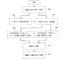
構造式(V)、(VI)、(VII)および(VIII)で表されるポリマーは、図2に示す4段階の工程により製造できる。 The polymers represented by structural formulas (V), (VI), (VII) and (VIII) can be produced by a four-step process shown in FIG.
S100では、塩基と有機溶媒の存在下で2モルの適切なニトリルまたはシッフ塩基と1モルのコハク酸ジエステルとを反応させることによりDPP部分を形成することができる。例えば、所望のAr基の形成用のカルボニトリル(Ar−CN)(例えば、チオフェンカルボニトリル)とコハク酸ジイソプロピルとをDPP部分の閉環のための適切な条件下で反応させて、下記一般式のモノマー(M1)を形成する。
S100では、インサイチューで(in situ)形成できるt−C5H11ONa等のナトリウムアルコキシドの存在下、溶液中で、約85℃で実施することができ、次いで氷酢酸等の有機酸で中和が行われる。米国特許第4579949号では、DPP分子形成の反応についてさらに詳細が述べられている。 In S100, it can be carried out in solution in the presence of a sodium alkoxide such as t-C 5 H 11 ONa, which can be formed in situ, at about 85 ° C. and then in an organic acid such as glacial acetic acid. Sum is done. US Pat. No. 4,579,949 provides further details on the reaction of DPP molecule formation.
S102では、S100で得られたモノマー(M1)のH基が所望のR基に変換されるが、その反応には式R−Yで表されるハロゲン化物(式中、RはH以外の上記で定義されたものであり、Yは塩素、臭素、およびヨウ素から選択できるハロゲンである)が用いられる。これにより、下記構造式(M2)のモノマーが形成される。
S102は、約40℃〜約180℃(例えば、約120℃)の温度で、溶液中で実施できる。反応は、ジメチルホルムアミドの等の好適な溶媒中で、アルカリ金属水酸化物や炭酸塩のような水性塩基、および18−クラウン−6等のクラウンエーテルの存在下で実施できる。好適な水性塩基としては、NaOH、KOH、Na2CO3、K2CO3等、例えばK2CO3水溶液が挙げられる。通常、化合物M1に対する塩基のモル比は0.5:1〜50:1の範囲から選択される。 S102 can be performed in solution at a temperature of about 40 ° C. to about 180 ° C. (eg, about 120 ° C.). The reaction can be carried out in a suitable solvent such as dimethylformamide in the presence of an aqueous base such as an alkali metal hydroxide or carbonate and a crown ether such as 18-crown-6. Suitable aqueous bases include NaOH, KOH, Na 2 CO 3 , K 2 CO 3 and the like, for example, an aqueous K 2 CO 3 solution. Usually, the molar ratio of base to compound M1 is selected from the range of 0.5: 1 to 50: 1.
S104では、S100またはS102で形成されるモノマー(M1)または(M2)とハロゲンとの反応によりAr基がハロゲン化され、下記一般式のモノマーを形成する。
式中、Yは例えば臭素、塩素またはヨウ素である。S104は、クロロホルム等の任意の好適な非反応性溶媒中で、例えば室温またはそれより高い温度で実施できる。 In the formula, Y is, for example, bromine, chlorine or iodine. S104 can be performed in any suitable non-reactive solvent such as chloroform, for example at room temperature or higher.
S106では、モノマー(M3)を重合して一般式(III)のホモポリマーが形成される。特に、Arが下記構造である場合、得られるポリマーは上記の構造(VIII)を有する。
あるいは、S108では、上記構造式(IV)、(V)または(VI)における単位Mを形成するためのチオフェン、フラン、ピロール、チエノ[3,2−b]チオフェン、ベンゾ[1,2−b:4,5−b’]ジチオフェンおよびそれらの混合物等のコモノマーとモノマー(M3)とを共重合させてもよい。 Alternatively, in S108, thiophene, furan, pyrrole, thieno [3,2-b] thiophene, benzo [1,2-b for forming the unit M in the structural formula (IV), (V) or (VI). : 4,5-b ′] comonomer such as dithiophene and a mixture thereof and the monomer (M3) may be copolymerized.
S106またはS108は、ヘキサメチルジスズ(hexamethylditin)、ヘキサ−n−ブチルジスズ(hexa−n−butylditin)、ヘキサフェニルジスズ(hexaphenylditin)のようなヘキサアルキルジスズ(hexaalkylditin)またはヘキサアリールジスズ(hexaarylditin)等のジスズ(ditin)化合物と、カップリング反応または重縮合反応に適した触媒とを用いて、場合によってヨウ化銅(I)の存在下で、溶液中で実施できる。カップリング触媒としてはパラジウムベースの触媒、例えば(Pd(PPh3)4)が使用でき、DPPモノマー:触媒のモル比は、1000:1〜10:1、例えば100:1〜30:1が可能である。溶媒としては、THFと1−メチル−2−ピロリジノン(NMP)の混合物が使用可能である。反応は、溶媒の沸点またはそれよりわずかに高い温度での還流下で実施できる。 S106 or S108 is a hexaalkylditin such as hexamethylditin, hexa-n-butylditin, hexaphenylditin or hexaarylditin. ) And a catalyst suitable for the coupling or polycondensation reaction, optionally in the presence of copper (I) iodide, in solution. The coupling catalyst can be a palladium-based catalyst, such as (Pd (PPh 3 ) 4 ), and the DPP monomer: catalyst molar ratio can be 1000: 1 to 10: 1, such as 100: 1 to 30: 1. It is. As the solvent, a mixture of THF and 1-methyl-2-pyrrolidinone (NMP) can be used. The reaction can be carried out under reflux at a temperature at or slightly above the boiling point of the solvent.
S110では、得られたポリマーは例えばソックスレー抽出によって精製できる。 In S110, the resulting polymer can be purified, for example, by Soxhlet extraction.
このようにして、重量平均分子量Mwが700〜1,000,000の範囲、例えば約5000以上である、ポリマーまたはコポリマーを形成することができる。 In this way, a polymer or copolymer having a weight average molecular weight Mw in the range of 700 to 1,000,000, for example about 5000 or more, can be formed.
S112では、上記ポリマーを含む層が半導体デバイスに組み込まれる。 In S112, the layer containing the polymer is incorporated into a semiconductor device.
図1に示されるタイプのOTFTを形成する際は、例えば得られたポリマー(III)、(IV)、(V)、(VI)、(VII)または(VIII)をジクロロベンゼン等の好適な溶媒に溶解し、得られた溶液を例えばスピンコーティング、キャスティング、真空蒸着等により誘電体層上に堆積させる。誘電体層としては、例えばドープされたシリコンウェハ上で成長させた酸化ケイ素層が用いられる。半導体ポリマーの堆積は環境条件下、例えば酸素が約5重量%を超えて存在するような大気中やその他の雰囲気中で、約25℃の温度で実施できる。また、堆積は雰囲気中の湿気を除去しなくても実施できる。例えば、堆積は約10%、またはそれ以上の相対湿度のもとでも実施できる。 In forming an OTFT of the type shown in FIG. 1, for example, the obtained polymer (III), (IV), (V), (VI), (VII) or (VIII) is replaced with a suitable solvent such as dichlorobenzene. And the resulting solution is deposited on the dielectric layer by, for example, spin coating, casting, vacuum evaporation or the like. For example, a silicon oxide layer grown on a doped silicon wafer is used as the dielectric layer. The deposition of the semiconducting polymer can be carried out at ambient temperatures, for example in the atmosphere or in other atmospheres where oxygen is present above about 5% by weight, at a temperature of about 25 ° C. Deposition can be performed without removing moisture in the atmosphere. For example, the deposition can be performed at a relative humidity of about 10% or higher.
半導体ポリマー層を堆積させる前に、誘電体層をオクチルトリクロロシラン等の反応性有機シランで改質することで、有機シランの薄層(例えば5nmの厚み)を誘電体層上に設けてもよい。 Prior to depositing the semiconductor polymer layer, the dielectric layer may be modified with a reactive organosilane such as octyltrichlorosilane to provide a thin layer of organosilane (eg 5 nm thick) on the dielectric layer. .
得られた半導体層は、次に例えば80℃の真空オーブン中で5〜10時間乾燥させる。次いで、例えばシャドーマスクを介して真空蒸着により半導体層の上面に金を堆積させて、ソース電極とドレイン電極とを半導体層上にパターン形成することができる。 The resulting semiconductor layer is then dried, for example, in a vacuum oven at 80 ° C. for 5-10 hours. Then, for example, gold is deposited on the upper surface of the semiconductor layer by vacuum vapor deposition through a shadow mask, and the source electrode and the drain electrode can be patterned on the semiconductor layer.
得られた半導体デバイスは、例えば140℃の好適な温度で10〜15分間、半導体ポリマーに損傷を与えないようにアニール処理してもよい。 The obtained semiconductor device may be annealed at a suitable temperature of, for example, 140 ° C. for 10 to 15 minutes so as not to damage the semiconductor polymer.
以下の実施例では、構造式(VIII)で表させる例示ポリマーを形成する反応スキーム、およびそれから形成されるOTFTを提供する。ただし、本発明の実施形態の範囲はこれにより制限されるものではない。
実施例1:ポリ(2,5−ジオクタデシル−3,6−ビス(チエニル−5−イル)−ジケトピロロピロールの合成
The following examples provide a reaction scheme for forming an exemplary polymer represented by Structural Formula (VIII), and an OTFT formed therefrom. However, the scope of the embodiment of the present invention is not limited thereby.
Example 1: Synthesis of poly (2,5-dioctadecyl-3,6-bis (thienyl-5-yl) -diketopyrrolopyrrole
例示ポリマー4の合成の概要をスキーム1に示す。
スキーム1
Scheme 1
<1>3,6−ビス−(チエニル)−ジケトピロロピロール(1)の合成 <1> Synthesis of 3,6-bis- (thienyl) -diketopyrrolopyrrole (1)
ナトリウム(3.45g、0.15mol)を60mLのt−アミルアルコールに加え、少量の塩化鉄(III)(50mg)を加えた。ナトリウムが見えなくなるまで、混合物を95〜102℃で1時間激しく攪拌した。溶液を85℃まで冷却した。得られた溶液に10.9g(0.1mol)の2−チオフェンカルボニトリルを加えた。次に、8.3g(0.04mol)のコハク酸ジイソプロピルを5mLのt−アミルアルコールに溶解させたものを、85℃で1時間かけて滴下して加えた。滴下が完了した後、混合物を2時間、85℃に保った。次に、反応混合物を50℃まで冷却し、50mLのメタノールで希釈し、次いで、約15mLの氷酢酸でゆっくり中和し、短時間還流して、反応混合物をろ過した。残渣を熱メタノールと水で数回洗浄し、得られた固体を真空下、50℃で乾燥した。青みがかった赤色固体(11g、収率92%)が得られた(化合物(1))。 Sodium (3.45 g, 0.15 mol) was added to 60 mL t-amyl alcohol and a small amount of iron (III) chloride (50 mg) was added. The mixture was stirred vigorously at 95-102 ° C. for 1 hour until no more sodium was visible. The solution was cooled to 85 ° C. 10.9 g (0.1 mol) of 2-thiophenecarbonitrile was added to the resulting solution. Next, 8.3 g (0.04 mol) of diisopropyl succinate dissolved in 5 mL of t-amyl alcohol was added dropwise at 85 ° C. over 1 hour. After the addition was complete, the mixture was kept at 85 ° C. for 2 hours. The reaction mixture was then cooled to 50 ° C., diluted with 50 mL of methanol, then slowly neutralized with about 15 mL of glacial acetic acid, refluxed briefly, and the reaction mixture was filtered. The residue was washed several times with hot methanol and water and the resulting solid was dried at 50 ° C. under vacuum. A bluish red solid (11 g, 92% yield) was obtained (compound (1)).
<2>2,5−ジオクタデシル−3,6−ビス−(チエニル)−ジケトピロロピロール(2) <2> 2,5-dioctadecyl-3,6-bis- (thienyl) -diketopyrrolopyrrole (2)
75mLのジメチルホルムアミド(DMF)に化合物(1)(1.5g、5mmol)、2.31g(16.7mmol)のK2CO3、12mgの18−クラウン−6、および1−ブロモオクタデカン(5.57g、16.7mmol)を混合したものを120℃で一晩加熱した。室温まで冷却した後、溶液をろ過し、固体を水で数回洗浄した。固体を加熱してクロロホルムに溶解し、ろ過した。ろ液を室温まで冷却し、赤色の沈殿を得た。固体をろ過し、真空下で乾燥した(化合物(2))。 In 75 mL of dimethylformamide (DMF) compound (1) (1.5 g, 5 mmol), 2.31 g (16.7 mmol) of K 2 CO 3 , 12 mg of 18-crown-6, and 1-bromooctadecane (5. 57 g, 16.7 mmol) was heated at 120 ° C. overnight. After cooling to room temperature, the solution was filtered and the solid was washed several times with water. The solid was heated to dissolve in chloroform and filtered. The filtrate was cooled to room temperature and a red precipitate was obtained. The solid was filtered and dried under vacuum (compound (2)).
<3>2,5−ジオクタデシル−3,6−ビス−(5−ブロモチエニル)−ジケトピロロピロール(3) <3> 2,5-dioctadecyl-3,6-bis- (5-bromothienyl) -diketopyrrolopyrrole (3)
化合物(2)(4.416g、3mmol)と30mLのクロロホルムを攪拌バー、冷却管、および添加用漏斗を装着した100mLの3口フラスコに入れた。次に、0.96g(6mmol)のBr2を20mLのクロロホルムに溶解したものをフラスコに室温で添加した。混合物を室温で10分間攪拌し、次に60℃に加温して、さらに1時間攪拌した。次に、反応混合物を室温まで冷却し、ろ過した。得られた赤色の固体をNa2SO3溶液と水とで洗浄し、最後にメタノールで十分に洗浄した。次いで、固体を加熱してクロロホルムに溶解し、次に室温まで冷却した。ろ過後に得られた暗紫色の固体を真空下で乾燥した。収率:1.78g(61.6%)。 1H NMR(CDCl3):8.69(d、J=4.2Hz、2H)、7.24(d、J=4.2Hz、2H)、3.98(t、J=7.7Hz、4H)、1.71(m、4H)、1.20−1.50(m、60H)、0.88(t、J=6.6Hz、6H)。融点:161℃。 Compound (2) (4.416 g, 3 mmol) and 30 mL of chloroform were placed in a 100 mL 3-neck flask equipped with a stir bar, condenser, and addition funnel. Next, 0.96 g (6 mmol) of Br 2 dissolved in 20 mL of chloroform was added to the flask at room temperature. The mixture was stirred at room temperature for 10 minutes, then warmed to 60 ° C. and stirred for an additional hour. The reaction mixture was then cooled to room temperature and filtered. The resulting red solid was washed with Na 2 SO 3 solution and water, and finally washed thoroughly with methanol. The solid was then heated to dissolve in chloroform and then cooled to room temperature. The dark purple solid obtained after filtration was dried under vacuum. Yield: 1.78 g (61.6%). 1 H NMR (CDCl 3 ): 8.69 (d, J = 4.2 Hz, 2H), 7.24 (d, J = 4.2 Hz, 2H), 3.98 (t, J = 7.7 Hz, 4H), 1.71 (m, 4H), 1.20-1.50 (m, 60H), 0.88 (t, J = 6.6 Hz, 6H). Melting point: 161 ° C.
<4>ポリ(2,5−ジオクタデシル−3,6−ビス(チエニル−5−イル)−ジケトピロロピロール)(4) <4> Poly (2,5-dioctadecyl-3,6-bis (thienyl-5-yl) -diketopyrrolopyrrole) (4)
ヘキサメチルジスズ(0.344g、1.05mmol)、テトラキス(トリフェニルホスフィン)パラジウム(0)、Pd(PPh3)4(58mg、0.05mmol)、ヨウ化銅(I)(3.8mg、0.02mmol)、上記化合物(3)(0.9631g、1mmol)、THF(30mL)および1−メチル−2−ピロリジノン(NMP)(15mL)を100mLのフラスコに入れた。反応混合物を加熱して48時間還流し、次に室温まで冷却し、200mLの攪拌しているアセトンに注ぎ込んだ。固体をろ過し、メタノールで洗浄して乾燥した。次いで、ヘプタンを用いたソックスレー抽出を48時間行って固体をさらに精製し、クロロベンゼンに溶解した。溶媒を除去して、暗青色の固体を得た(0.50g、62.5%)(化合物(4))。 Hexamethyldistin (0.344 g, 1.05 mmol), tetrakis (triphenylphosphine) palladium (0), Pd (PPh 3 ) 4 (58 mg, 0.05 mmol), copper (I) iodide (3.8 mg, 0.02 mmol), the above compound (3) (0.9631 g, 1 mmol), THF (30 mL) and 1-methyl-2-pyrrolidinone (NMP) (15 mL) were placed in a 100 mL flask. The reaction mixture was heated to reflux for 48 hours, then cooled to room temperature and poured into 200 mL of stirred acetone. The solid was filtered, washed with methanol and dried. Subsequently, Soxhlet extraction with heptane was performed for 48 hours, and the solid was further purified and dissolved in chlorobenzene. Removal of the solvent gave a dark blue solid (0.50 g, 62.5%) (compound (4)).
実施例2:OTFTの製造および特性評価 Example 2: Manufacture and characterization of OTFT
図1に概略的に示されるトップコンタクト型の薄膜トランジスタの構成を試験用デバイス構造として選択した。試験用デバイスは、nドープされたシリコンウェハ上に厚さ約200ナノメートルの熱的に成長した酸化ケイ素層20を設けたものの上に形成し、静電容量計で測定した静電容量は約15nF/cm2(ナノファラッド/平方センチメートル)であった。ウェハはゲート電極の機能を果たし、酸化ケイ素はゲート誘電体の役割を果たす。
The configuration of the top contact thin film transistor schematically shown in FIG. 1 was selected as the test device structure. The test device was formed on an n-doped silicon wafer provided with a thermally grown
酸化ケイ素層が設けられたnドープシリコンウェハは、初めにイソプロパノール、アルゴンプラズマ、イソプロパノールでそれぞれ洗浄し、その後空気乾燥し、0.1Mのオクチルトリクロロシラン(OTS−8)のトルエン溶液に60℃で20分浸漬した。続いて、ウェハをトルエン、イソプロパノールで洗浄し、空気乾燥した。ポリマー(4)(ポリ(2,5−ジオクタデシル−3,6−ビス−(チエニル−5−イル)−ジケトピロロピロール)をジクロロベンゼンに溶解した溶液(0.5重量%)を初めに1.0マイクロメートルのシリンジフィルターでろ過し、次いでOTS−8処理したシリコンウェハ上に1000rpm、室温で120秒間スピンコーティングした。これにより、厚みが20〜50nmの半導体層がシリコンウェハ上に形成され、これを真空オーブン内で、80℃で5〜10時間乾燥した。引き続き、シャドーマスクを介して真空蒸着することで、チャネル長さと幅の様々に異なる、厚みが約50ナノメートルの金のソース電極およびドレイン電極を半導体層の上面に形成した。これにより、種々の大きさの一連のトランジスタを作成した。デバイスの評価は、140℃で10〜15分アニール処理してから行った。 The n-doped silicon wafer provided with the silicon oxide layer is first cleaned with isopropanol, argon plasma, and isopropanol, then air-dried, and then added to a 0.1 M octyltrichlorosilane (OTS-8) toluene solution at 60 ° C. Soaked for 20 minutes. Subsequently, the wafer was washed with toluene and isopropanol and air-dried. First, a solution (0.5% by weight) of polymer (4) (poly (2,5-dioctadecyl-3,6-bis- (thienyl-5-yl) -diketopyrrolopyrrole) dissolved in dichlorobenzene was used. It was filtered with a 1.0 micrometer syringe filter and then spin-coated on an OTS-8 treated silicon wafer at 1000 rpm and room temperature for 120 seconds, thereby forming a semiconductor layer having a thickness of 20-50 nm on the silicon wafer. This was dried in a vacuum oven for 5-10 hours at 80 ° C. Subsequently, vacuum deposition through a shadow mask was used to vary the channel length and width, and the gold source was about 50 nanometers thick. An electrode and a drain electrode were formed on the upper surface of the semiconductor layer, thereby creating a series of transistors of various sizes. Evaluation of chair was performed after 10 to 15 minutes annealing at 140 ° C..
トランジスタ性能の評価は暗箱(すなわち、環境光を排除した密閉された箱)内で、Keithley 4200 SCS半導体特性評価システムを用いて環境条件下で行った。キャリア移動度μを、飽和領域(ゲート電圧、VG<ソース−ドレイン電圧、VSD)のデータから下記方程式(1)に基づいて計算した。
ISD=Ciμ(W/2L)(VG−VT)2 (1)
式中、ISDは飽和領域のドレイン電流、WおよびLはそれぞれ半導体チャネルの幅および長さ、Ciはゲート誘電体層20の単位面積あたりの静電容量、VGとVTはそれぞれゲート電圧としきい電圧である。デバイスのVTは、飽和領域におけるISDの平方根とデバイスのVGとの関係から、測定されたデータをIID=0まで外挿することによって決定された。
The transistor performance was evaluated in a dark box (that is, a sealed box that excluded ambient light) under environmental conditions using a Keithley 4200 SCS semiconductor characterization system. The carrier mobility μ was calculated based on the following equation (1) from data in the saturation region (gate voltage, V G <source-drain voltage, V SD ).
I SD = C i μ (W / 2L) (V G −V T ) 2 (1)
Where I SD is the drain current of the saturation region, W and L are the width and length of the semiconductor channel, C i is the capacitance per unit area of the
デバイスの移動特性と出力特性は、化合物(4)がp型半導体であることを示した。W=5000μm、L=90μmの寸法のトランジスタを用いて、5個以上のトランジスタから以下の平均特性値が得られた。
移動度:0.08〜0.12cm2/V.s.
オン/オフ比:106
The mobility and output characteristics of the device indicated that compound (4) is a p-type semiconductor. Using the transistors having dimensions of W = 5000 μm and L = 90 μm, the following average characteristic values were obtained from five or more transistors.
Mobility: 0.08-0.12 cm < 2 > / V. s.
On / off ratio: 10 6
移動度およびオン/オフ比はポリチオフェン(例えば、ポリ(3−ヘキシルチオフェン)(P3HT)やポリ[チオフェン](PQT))のそれと同程度である。OTFTデバイスは全て環境条件下で生成、測定され、この種のポリマーの優れた空気安定性を示した。 The mobility and on / off ratio are comparable to those of polythiophene (eg, poly (3-hexylthiophene) (P3HT) or poly [thiophene] (PQT)). All OTFT devices were produced and measured under environmental conditions and showed excellent air stability of this type of polymer.
Claims (4)
a)下式で表されるモノマーを重合、または下式で表されるモノマーとコモノマーとを重合させてポリマーを形成する工程と、
b)前記ポリマーを含むポリマー材料の薄膜トランジスタの半導体層を形成する工程と、を含む方法。
a) polymerizing a monomer represented by the following formula, or polymerizing a monomer represented by the following formula and a comonomer to form a polymer;
b) forming a semiconductor layer of a thin film transistor of a polymer material containing the polymer.
Applications Claiming Priority (1)
| Application Number | Priority Date | Filing Date | Title |
|---|---|---|---|
| US11/850,915 US7910684B2 (en) | 2007-09-06 | 2007-09-06 | Diketopyrrolopyrrole-based derivatives for thin film transistors |
Publications (2)
| Publication Number | Publication Date |
|---|---|
| JP2009135422A true JP2009135422A (en) | 2009-06-18 |
| JP2009135422A5 JP2009135422A5 (en) | 2011-07-14 |
Family
ID=40019432
Family Applications (1)
| Application Number | Title | Priority Date | Filing Date |
|---|---|---|---|
| JP2008228383A Pending JP2009135422A (en) | 2007-09-06 | 2008-09-05 | Thin-film transistor and method of forming the same |
Country Status (4)
| Country | Link |
|---|---|
| US (1) | US7910684B2 (en) |
| EP (1) | EP2034537A3 (en) |
| JP (1) | JP2009135422A (en) |
| TW (1) | TWI466915B (en) |
Cited By (17)
| Publication number | Priority date | Publication date | Assignee | Title |
|---|---|---|---|---|
| WO2012032949A1 (en) * | 2010-09-10 | 2012-03-15 | 住友化学株式会社 | Polymer compound and organic photoelectric transducer |
| JP2012506928A (en) * | 2008-10-31 | 2012-03-22 | ビーエーエスエフ ソシエタス・ヨーロピア | Diketopyrrolopyrrole polymers for use in organic field effect transistors |
| JP2012506930A (en) * | 2008-10-31 | 2012-03-22 | ビーエーエスエフ ソシエタス・ヨーロピア | Diketopyrrolopyrrole polymers for use in organic semiconductor devices |
| WO2012050070A1 (en) * | 2010-10-13 | 2012-04-19 | 住友化学株式会社 | High molecular compound and organic photoelectric conversion element using same |
| WO2012060283A1 (en) * | 2010-11-02 | 2012-05-10 | 住友化学株式会社 | Macromolecular compound and organic photoelectric conversion element using same |
| JP2012521462A (en) * | 2009-03-23 | 2012-09-13 | ビーエーエスエフ ソシエタス・ヨーロピア | Diketopyrrolopyrrole polymers for use in organic semiconductor devices |
| JP2012528215A (en) * | 2009-05-27 | 2012-11-12 | ビーエーエスエフ ソシエタス・ヨーロピア | Diketopyrrolopyrrole polymers for use in organic semiconductor devices |
| WO2012165128A1 (en) * | 2011-05-27 | 2012-12-06 | 住友化学株式会社 | High-molecular-weight compound and organic photoelectric conversion element |
| JP2013525514A (en) * | 2010-03-20 | 2013-06-20 | ポリエラ コーポレイション | Pyrrolo [3,2-b] pyrrole semiconductor compound and device incorporating the same |
| JP2013533895A (en) * | 2010-05-19 | 2013-08-29 | ビーエーエスエフ ソシエタス・ヨーロピア | Diketopyrrolopyrrole-based polymers for use in organic semiconductor devices |
| JP2014528908A (en) * | 2011-06-22 | 2014-10-30 | ビーエーエスエフ ソシエタス・ヨーロピアBasf Se | Diketopyrrolopyrrole oligomers for use in organic semiconductor devices |
| JP2014533303A (en) * | 2011-09-02 | 2014-12-11 | ビーエーエスエフ ソシエタス・ヨーロピアBasf Se | Diketopyrrolopyrrole oligomer and composition comprising diketopyrrolopyrrole oligomer |
| JP2015507840A (en) * | 2011-12-07 | 2015-03-12 | ビーエーエスエフ ソシエタス・ヨーロピアBasf Se | Organic field effect transistor |
| WO2015147459A1 (en) * | 2014-03-24 | 2015-10-01 | 경상대학교산학협력단 | Asymmetric diketopyrrolopyrrole polymer and organic electronic device containing same |
| JPWO2015076171A1 (en) * | 2013-11-21 | 2017-03-16 | 株式会社ダイセル | Solvent for organic transistor manufacturing |
| JPWO2017038944A1 (en) * | 2015-09-02 | 2018-06-14 | 富士フイルム株式会社 | Organic thin film transistor, organic thin film transistor manufacturing method, organic semiconductor composition, organic semiconductor film, and organic semiconductor film manufacturing method |
| JPWO2017038948A1 (en) * | 2015-09-02 | 2018-06-28 | 富士フイルム株式会社 | Organic thin film transistor, organic thin film transistor manufacturing method, organic semiconductor composition, organic semiconductor film, and organic semiconductor film manufacturing method |
Families Citing this family (46)
| Publication number | Priority date | Publication date | Assignee | Title |
|---|---|---|---|---|
| CA2655076A1 (en) | 2006-06-30 | 2008-01-03 | Ciba Holding Inc. | Diketopyrrolopyrrole polymers as organic semiconductors |
| KR101546985B1 (en) | 2007-10-09 | 2015-08-24 | 바스프 에스이 | Pyrrolopyrrole derivatives, their manufacture and use |
| WO2009104781A1 (en) * | 2008-02-18 | 2009-08-27 | 住友化学株式会社 | Composition and organic photoelectric converter using the same |
| JP4995909B2 (en) * | 2008-04-18 | 2012-08-08 | 三菱レイヨン株式会社 | Carbon fiber yarn manufacturing apparatus and manufacturing method |
| US10224484B2 (en) * | 2008-10-31 | 2019-03-05 | Basf Se | Diketopyrrolopyrrole polymers for use in organic field effect transistors |
| JP5623512B2 (en) | 2009-05-27 | 2014-11-12 | ビーエーエスエフ ソシエタス・ヨーロピアBasf Se | (Heterocyclic) aromatic compound polymerization method |
| US9166167B2 (en) | 2009-08-28 | 2015-10-20 | Agency For Science, Technology And Research | P-type materials and organic electronic devices |
| JP5653436B2 (en) | 2009-08-28 | 2015-01-14 | エージェンシー フォー サイエンス, テクノロジー アンド リサーチ | Polymer semiconductors, devices, and related methods |
| CN102812016B (en) | 2009-09-04 | 2015-12-09 | 索尔维美国有限公司 | Comprise photovoltaic cell and based on the organic electronic device of the polymkeric substance of diketone and polymkeric substance |
| CN102276804B (en) * | 2010-06-13 | 2013-04-17 | 海洋王照明科技股份有限公司 | Perylene tetracarboxylic diimide copolymer containing dithiophen-pyrrole unit and preparation method and application thereof |
| WO2011161078A1 (en) | 2010-06-24 | 2011-12-29 | Basf Se | An organic field effect transistor with improved current on/off ratio and controllable threshold shift |
| CN102344549B (en) * | 2010-07-30 | 2013-07-10 | 海洋王照明科技股份有限公司 | Porphyrin-pyrrolopyrrole copolymer containing carbazole, preparation method thereof and application thereof |
| CN102372842B (en) * | 2010-08-19 | 2013-06-05 | 海洋王照明科技股份有限公司 | Copolymer containing thiophene pyrroledione units, and preparation method and application thereof |
| KR101880777B1 (en) | 2010-09-29 | 2018-08-17 | 바스프 에스이 | Semiconductors based on diketopyrrolopyrroles |
| US8946376B2 (en) | 2010-09-29 | 2015-02-03 | Basf Se | Semiconductors based on diketopyrrolopyrroles |
| CN103262280A (en) | 2010-12-22 | 2013-08-21 | 巴斯夫欧洲公司 | Semiconductor structure and method for its production |
| WO2012129511A2 (en) * | 2011-03-24 | 2012-09-27 | Northwestern University | Semiconducting compounds and devices incorporating same |
| WO2012146574A1 (en) * | 2011-04-28 | 2012-11-01 | Basf Se | Semiconductor materials based on diketopiperidinopiperidine copolymers |
| TW201321427A (en) * | 2011-08-19 | 2013-06-01 | Univ Washington | New poly(heteroarylene vinylene)s based on diketopyrrolopyrrole |
| US8846855B2 (en) | 2011-10-31 | 2014-09-30 | Corning Incorporated | Conjugated fused thiophenes, methods of making conjugated fused thiophenes, and uses thereof |
| US8901544B2 (en) | 2011-12-06 | 2014-12-02 | Corning Incorporated | Organic thin film transistor with ion exchanged glass substrate |
| US8598299B2 (en) | 2011-12-06 | 2013-12-03 | Xerox Corporation | Semiconductor composition |
| EP2789024B1 (en) | 2011-12-07 | 2015-11-18 | Basf Se | Diketopyrrolopyrrole polymers for use in organic semiconductor devices |
| CN103304780B (en) * | 2012-03-16 | 2015-07-01 | 中国科学院化学研究所 | Ethylene-DPP (Dipeptidyl Peptidase)-based copolymer with big circumference ratio (pi) as well as preparation method and application thereof |
| US8563851B2 (en) | 2012-03-19 | 2013-10-22 | Xerox Corporation | Method to increase field effect mobility of donor-acceptor semiconductors |
| US8558109B2 (en) | 2012-03-19 | 2013-10-15 | Xerox Corporation | Semiconductor composition for high performance organic devices |
| JP6419065B2 (en) | 2012-04-02 | 2018-11-07 | ビーエーエスエフ ソシエタス・ヨーロピアBasf Se | Phenanthro [9,10-b] furan polymers and small molecule compounds for electronics applications |
| EP2834286B1 (en) * | 2012-04-04 | 2019-01-23 | Basf Se | Diketopyrrolopyrrole polymers and small molecules |
| WO2014016219A1 (en) | 2012-07-23 | 2014-01-30 | Basf Se | Dithienobenzofuran polymers and small molecules for electronic application |
| CN103012751B (en) * | 2012-11-30 | 2015-05-20 | 四川大学 | Preparation method of bis-thienyl pyrrolo-[3,4-c] pyrrole-1,4-diketone and (hybrid) arene copolymer |
| JP6270867B2 (en) | 2012-12-04 | 2018-01-31 | ビーエーエスエフ ソシエタス・ヨーロピアBasf Se | Functionalized benzodithiophene polymers for electronics applications |
| US9214258B2 (en) | 2012-12-06 | 2015-12-15 | Xerox Corporation | Semiconductor composites comprising carbon nanotubes and diketopyrrolopyrrole-thiophene based copolymers |
| US8575477B1 (en) | 2012-12-27 | 2013-11-05 | Xerox Corporation | Diketopyrrolopyrrole-based polymers containing a diene group for semiconductors |
| US8865861B2 (en) | 2012-12-27 | 2014-10-21 | Xerox Corporation | Pechmann dye based polymers and semiconductor compositions |
| US8809484B2 (en) | 2012-12-27 | 2014-08-19 | Xerox Corporation | Extended isoindigo polymers and semiconductor compositions |
| KR101485398B1 (en) * | 2013-05-07 | 2015-01-26 | 경상대학교산학협력단 | Diketopyrrolopyrrole polymer and organic electronic device using the same |
| US9761803B2 (en) | 2013-07-22 | 2017-09-12 | Xerox Corporation | Semiconductor composition |
| US20160272656A1 (en) * | 2013-10-28 | 2016-09-22 | Keun Cho | Single molecule and organic solar cell comprising same |
| US9399698B2 (en) | 2014-01-31 | 2016-07-26 | Xerox Corporation | Processes for purifying diketopyrrolopyrrole copolymers |
| KR102099612B1 (en) * | 2014-03-27 | 2020-04-10 | 경상대학교산학협력단 | Diketopyrrolopyrrole polymer and organic electronic device using the same |
| US9580556B2 (en) | 2015-01-29 | 2017-02-28 | Corning Incorporated | DPP with branched alkyl-chain or (and) fused thiophene with branched alkyl-chain and the related designing strategy to increase the molecular weight of their semi-conducting copolymers |
| CN104774319B (en) * | 2015-04-08 | 2017-02-01 | 中国科学院化学研究所 | Bis(benzothiophene) ethylene polymers and preparation method and application thereof |
| US10109798B2 (en) * | 2015-05-26 | 2018-10-23 | Purdue Research Foundation | Methods and compositions for enhancing processability and charge transport of polymer semiconductors |
| WO2018070670A1 (en) * | 2016-10-11 | 2018-04-19 | 이화여자대학교 산학협력단 | Organic semiconductor compound and electronic device using same |
| CN106750193A (en) * | 2016-12-12 | 2017-05-31 | 中国科学院化学研究所 | Even tripyrrole and pyrroledione polymer and its synthetic method and application |
| CN115385921B (en) * | 2022-09-29 | 2024-04-16 | 天津大学 | Preparation method of thiazole-5-pyrrolopyrrole diketone and conjugated polymer thereof and application of thiazole-5-pyrrolopyrrole diketone as semiconductor material |
Citations (5)
| Publication number | Priority date | Publication date | Assignee | Title |
|---|---|---|---|---|
| JP2004006782A (en) * | 2002-04-11 | 2004-01-08 | Konica Minolta Holdings Inc | Organic semiconductor material, organic transistor, field effect transistor and switching element employing it |
| JP2005206750A (en) * | 2004-01-26 | 2005-08-04 | Konica Minolta Holdings Inc | Organic semiconductive material, organic transistor, field-effect transistor, switching element, and five-membered heterocyclic compound |
| JP2006232898A (en) * | 2005-02-23 | 2006-09-07 | Ricoh Co Ltd | Electroconductive polymer material, field-effect transistor using the same and method for producing the same |
| JP2007088223A (en) * | 2005-09-22 | 2007-04-05 | Konica Minolta Holdings Inc | Organic semiconductor material, organic semiconductor film, organic semiconductor device and organic thin film transistor |
| JP2007516315A (en) * | 2003-10-28 | 2007-06-21 | チバ スペシャルティ ケミカルズ ホールディング インコーポレーテッド | New diketopyrrolopyrrole polymer |
Family Cites Families (15)
| Publication number | Priority date | Publication date | Assignee | Title |
|---|---|---|---|---|
| EP0061426B1 (en) | 1981-03-20 | 1985-02-13 | Ciba-Geigy Ag | Process for colouring highly molecular organic material and polycyclic pigments |
| US4579949A (en) | 1982-05-17 | 1986-04-01 | Ciba-Geigy Corporation | Preparation of pyrrolo[3,4-c]pyrroles |
| US6107117A (en) | 1996-12-20 | 2000-08-22 | Lucent Technologies Inc. | Method of making an organic thin film transistor |
| TWI290164B (en) | 1999-08-26 | 2007-11-21 | Ciba Sc Holding Ag | DPP-containing conjugated polymers and electroluminescent devices |
| EP1078970B1 (en) * | 1999-08-26 | 2004-03-17 | Ciba SC Holding AG | DPP-containing conjugated polymers and electroluminescent devices |
| US6683333B2 (en) * | 2000-07-14 | 2004-01-27 | E Ink Corporation | Fabrication of electronic circuit elements using unpatterned semiconductor layers |
| JP4997688B2 (en) | 2003-08-19 | 2012-08-08 | セイコーエプソン株式会社 | Electrode, thin film transistor, electronic circuit, display device and electronic device |
| DE602004017550D1 (en) | 2003-08-28 | 2008-12-18 | Merck Patent Gmbh | Mono-, Oligo- and Polythienoi2,3-b thiophenes |
| JP4795634B2 (en) * | 2003-10-31 | 2011-10-19 | 出光興産株式会社 | Organic thin film transistor |
| US7170093B2 (en) | 2004-11-05 | 2007-01-30 | Xerox Corporation | Dielectric materials for electronic devices |
| JP4911486B2 (en) * | 2005-04-13 | 2012-04-04 | 東洋インキScホールディングス株式会社 | Organic transistor |
| US7919573B2 (en) | 2005-11-16 | 2011-04-05 | Xerox Corporation | Polymer having thieno[3,2-b] thiophene moieties |
| US7425723B2 (en) | 2005-12-21 | 2008-09-16 | Xerox Corporation | Organic thin-film transistors |
| US7632703B2 (en) | 2005-12-22 | 2009-12-15 | Xerox Corporation | Organic thin-film transistors |
| CA2655076A1 (en) | 2006-06-30 | 2008-01-03 | Ciba Holding Inc. | Diketopyrrolopyrrole polymers as organic semiconductors |
-
2007
- 2007-09-06 US US11/850,915 patent/US7910684B2/en active Active
-
2008
- 2008-07-22 EP EP08160872A patent/EP2034537A3/en not_active Ceased
- 2008-09-04 TW TW97133847A patent/TWI466915B/en not_active IP Right Cessation
- 2008-09-05 JP JP2008228383A patent/JP2009135422A/en active Pending
Patent Citations (5)
| Publication number | Priority date | Publication date | Assignee | Title |
|---|---|---|---|---|
| JP2004006782A (en) * | 2002-04-11 | 2004-01-08 | Konica Minolta Holdings Inc | Organic semiconductor material, organic transistor, field effect transistor and switching element employing it |
| JP2007516315A (en) * | 2003-10-28 | 2007-06-21 | チバ スペシャルティ ケミカルズ ホールディング インコーポレーテッド | New diketopyrrolopyrrole polymer |
| JP2005206750A (en) * | 2004-01-26 | 2005-08-04 | Konica Minolta Holdings Inc | Organic semiconductive material, organic transistor, field-effect transistor, switching element, and five-membered heterocyclic compound |
| JP2006232898A (en) * | 2005-02-23 | 2006-09-07 | Ricoh Co Ltd | Electroconductive polymer material, field-effect transistor using the same and method for producing the same |
| JP2007088223A (en) * | 2005-09-22 | 2007-04-05 | Konica Minolta Holdings Inc | Organic semiconductor material, organic semiconductor film, organic semiconductor device and organic thin film transistor |
Cited By (21)
| Publication number | Priority date | Publication date | Assignee | Title |
|---|---|---|---|---|
| JP2012506928A (en) * | 2008-10-31 | 2012-03-22 | ビーエーエスエフ ソシエタス・ヨーロピア | Diketopyrrolopyrrole polymers for use in organic field effect transistors |
| JP2012506930A (en) * | 2008-10-31 | 2012-03-22 | ビーエーエスエフ ソシエタス・ヨーロピア | Diketopyrrolopyrrole polymers for use in organic semiconductor devices |
| KR101754432B1 (en) | 2009-03-23 | 2017-07-05 | 바스프 에스이 | Diketopyrrolopyrrole polymers for use in organic semiconductor devices |
| JP2012521462A (en) * | 2009-03-23 | 2012-09-13 | ビーエーエスエフ ソシエタス・ヨーロピア | Diketopyrrolopyrrole polymers for use in organic semiconductor devices |
| JP2012528215A (en) * | 2009-05-27 | 2012-11-12 | ビーエーエスエフ ソシエタス・ヨーロピア | Diketopyrrolopyrrole polymers for use in organic semiconductor devices |
| JP2013525514A (en) * | 2010-03-20 | 2013-06-20 | ポリエラ コーポレイション | Pyrrolo [3,2-b] pyrrole semiconductor compound and device incorporating the same |
| JP2013533895A (en) * | 2010-05-19 | 2013-08-29 | ビーエーエスエフ ソシエタス・ヨーロピア | Diketopyrrolopyrrole-based polymers for use in organic semiconductor devices |
| KR101839636B1 (en) * | 2010-05-19 | 2018-03-16 | 바스프 에스이 | Diketopyrrolopyrrole polymers for use in organic semiconductor devices |
| WO2012032949A1 (en) * | 2010-09-10 | 2012-03-15 | 住友化学株式会社 | Polymer compound and organic photoelectric transducer |
| WO2012050070A1 (en) * | 2010-10-13 | 2012-04-19 | 住友化学株式会社 | High molecular compound and organic photoelectric conversion element using same |
| WO2012060283A1 (en) * | 2010-11-02 | 2012-05-10 | 住友化学株式会社 | Macromolecular compound and organic photoelectric conversion element using same |
| WO2012165128A1 (en) * | 2011-05-27 | 2012-12-06 | 住友化学株式会社 | High-molecular-weight compound and organic photoelectric conversion element |
| JP2014528908A (en) * | 2011-06-22 | 2014-10-30 | ビーエーエスエフ ソシエタス・ヨーロピアBasf Se | Diketopyrrolopyrrole oligomers for use in organic semiconductor devices |
| JP2014533303A (en) * | 2011-09-02 | 2014-12-11 | ビーエーエスエフ ソシエタス・ヨーロピアBasf Se | Diketopyrrolopyrrole oligomer and composition comprising diketopyrrolopyrrole oligomer |
| JP2015507840A (en) * | 2011-12-07 | 2015-03-12 | ビーエーエスエフ ソシエタス・ヨーロピアBasf Se | Organic field effect transistor |
| JPWO2015076171A1 (en) * | 2013-11-21 | 2017-03-16 | 株式会社ダイセル | Solvent for organic transistor manufacturing |
| WO2015147459A1 (en) * | 2014-03-24 | 2015-10-01 | 경상대학교산학협력단 | Asymmetric diketopyrrolopyrrole polymer and organic electronic device containing same |
| KR20150110127A (en) * | 2014-03-24 | 2015-10-02 | 경상대학교산학협력단 | Asymmetric diketopyrrolopyrrole polymer and organic electronic device using the same |
| KR101600031B1 (en) | 2014-03-24 | 2016-03-07 | 경상대학교산학협력단 | Asymmetric diketopyrrolopyrrole polymer and organic electronic device using the same |
| JPWO2017038944A1 (en) * | 2015-09-02 | 2018-06-14 | 富士フイルム株式会社 | Organic thin film transistor, organic thin film transistor manufacturing method, organic semiconductor composition, organic semiconductor film, and organic semiconductor film manufacturing method |
| JPWO2017038948A1 (en) * | 2015-09-02 | 2018-06-28 | 富士フイルム株式会社 | Organic thin film transistor, organic thin film transistor manufacturing method, organic semiconductor composition, organic semiconductor film, and organic semiconductor film manufacturing method |
Also Published As
| Publication number | Publication date |
|---|---|
| EP2034537A3 (en) | 2009-06-24 |
| EP2034537A2 (en) | 2009-03-11 |
| TWI466915B (en) | 2015-01-01 |
| US20090065878A1 (en) | 2009-03-12 |
| TW200920761A (en) | 2009-05-16 |
| US7910684B2 (en) | 2011-03-22 |
Similar Documents
| Publication | Publication Date | Title |
|---|---|---|
| JP5311936B2 (en) | Diketopyrrolopyrrole polymer and method for forming the same | |
| JP2009135422A (en) | Thin-film transistor and method of forming the same | |
| Sonar et al. | Furan containing diketopyrrolopyrrole copolymers: synthesis, characterization, organic field effect transistor performance and photovoltaic properties | |
| US8871884B2 (en) | Copolymer semiconductors comprising thiazolothiazole or benzobisthiazole, or benzobisoxazole electron acceptor subunits, and electron donor subunits, and their uses in transistors and solar cells | |
| TWI535752B (en) | Polymer and organic solar cell comprising the same | |
| Hwang et al. | New thienothiadiazole-based conjugated copolymers for electronics and optoelectronics | |
| JP5728003B2 (en) | Condensed bithiophene vinylene copolymer | |
| Patil et al. | Synthesis and photovoltaic properties of narrow band gap copolymers of dithieno [3, 2-b: 2′, 3′-d] thiophene and diketopyrrolopyrrole | |
| KR20130069446A (en) | Novel diketopyrrolopyrrole polymers and organic electronic device using the same | |
| KR101151082B1 (en) | Star-shaped (Oligothiophene-Arylene) derivatives and Organic Thin Film Transistor using the same | |
| Gu et al. | Synthesis and photovoltaic properties of conjugated side chains polymers with different electron‐withdrawing and donating end groups | |
| CA2797308C (en) | Semiconductor composition | |
| Kim et al. | New quinoxaline derivatives as accepting units in donor–acceptor type low‐band gap polymers for organic photovoltaic cells | |
| JP5946273B2 (en) | Organic semiconductor compound, and transistor and electronic device including the same | |
| KR101630173B1 (en) | Asymmetric heterocycle-vinylene-heterocycle based diketopyrrolopyrrole polymer, organic electronic device using the same and monomer for preparing the same | |
| KR101589048B1 (en) | Novel organic semiconductor compound and organic electronic device using the same | |
| Yang et al. | Synthesis and photovoltaic properties of benzotriazole-based donor–acceptor copolymers | |
| Huang et al. | Low band‐gap D–A conjugated copolymers based on anthradithiophene and diketopyrrolopyrrole for polymer solar cells and field‐effect transistors | |
| Kong et al. | Anthradithiophene–thiophene copolymers with broad UV–vis absorption for organic solar cells and field‐effect transistors | |
| Truong et al. | Synthesis, characterization, and application to polymer solar cells of polythiophene derivatives with ester‐or ketone‐substituted phenyl side groups | |
| KR20150111094A (en) | Diketopyrrolopyrrole polymer and organic electronic device using the same | |
| KR101513883B1 (en) | Novel polymer and organic electronic device using the same | |
| KR20160088257A (en) | Asymmetric heterocycle-vinylene-heterocycle based diketopyrrolopyrrole polymer, organic electronic device using the same and monomer for preparing the same |
Legal Events
| Date | Code | Title | Description |
|---|---|---|---|
| A521 | Request for written amendment filed |
Free format text: JAPANESE INTERMEDIATE CODE: A523 Effective date: 20110601 |
|
| A621 | Written request for application examination |
Free format text: JAPANESE INTERMEDIATE CODE: A621 Effective date: 20110601 |
|
| A871 | Explanation of circumstances concerning accelerated examination |
Free format text: JAPANESE INTERMEDIATE CODE: A871 Effective date: 20110601 |
|
| A131 | Notification of reasons for refusal |
Free format text: JAPANESE INTERMEDIATE CODE: A131 Effective date: 20110712 |
|
| A975 | Report on accelerated examination |
Free format text: JAPANESE INTERMEDIATE CODE: A971005 Effective date: 20110704 |
|
| A601 | Written request for extension of time |
Free format text: JAPANESE INTERMEDIATE CODE: A601 Effective date: 20111012 |
|
| A602 | Written permission of extension of time |
Free format text: JAPANESE INTERMEDIATE CODE: A602 Effective date: 20111017 |
|
| A521 | Request for written amendment filed |
Free format text: JAPANESE INTERMEDIATE CODE: A523 Effective date: 20111024 |
|
| A131 | Notification of reasons for refusal |
Free format text: JAPANESE INTERMEDIATE CODE: A131 Effective date: 20111115 |
|
| A521 | Request for written amendment filed |
Free format text: JAPANESE INTERMEDIATE CODE: A523 Effective date: 20120206 |
|
| A02 | Decision of refusal |
Free format text: JAPANESE INTERMEDIATE CODE: A02 Effective date: 20120228 |