JP2009131911A - Manufacturing method of sealed device, and sealed device - Google Patents
Manufacturing method of sealed device, and sealed device Download PDFInfo
- Publication number
- JP2009131911A JP2009131911A JP2007307941A JP2007307941A JP2009131911A JP 2009131911 A JP2009131911 A JP 2009131911A JP 2007307941 A JP2007307941 A JP 2007307941A JP 2007307941 A JP2007307941 A JP 2007307941A JP 2009131911 A JP2009131911 A JP 2009131911A
- Authority
- JP
- Japan
- Prior art keywords
- bonding film
- manufacturing
- bonding
- film
- support
- Prior art date
- Legal status (The legal status is an assumption and is not a legal conclusion. Google has not performed a legal analysis and makes no representation as to the accuracy of the status listed.)
- Withdrawn
Links
Images


Classifications
-
- H—ELECTRICITY
- H01—ELECTRIC ELEMENTS
- H01L—SEMICONDUCTOR DEVICES NOT COVERED BY CLASS H10
- H01L2924/00—Indexing scheme for arrangements or methods for connecting or disconnecting semiconductor or solid-state bodies as covered by H01L24/00
- H01L2924/15—Details of package parts other than the semiconductor or other solid state devices to be connected
- H01L2924/161—Cap
- H01L2924/1615—Shape
- H01L2924/16195—Flat cap [not enclosing an internal cavity]
Abstract
Description
本発明は、封止型デバイスの製造方法および封止型デバイスに関するものである。 The present invention relates to a method for manufacturing a sealed device and a sealed device.
例えば、レーザープリンタ等にて光走査により描画を行うための光スキャナとして、捩り振動子で構成されたアクチュエータを用いたものが知られている(例えば、特許文献1参照。)。
特許文献1には、第1の振動系とこれに連結された第2の振動系とからなる2自由度振動系を有する基体と、この基体を支持する底部材および蓋部材と、2自由度振動系を駆動する圧電アクチュエータとを備えるアクチュエータが開示されている。
そして、第2の振動系には光反射部が設けられており、圧電アクチュエータの駆動力により第1の振動系を回動駆動させることにより、これに伴って、第2の振動系を回動駆動させて、光反射部で反射した光を走査する。これにより、光走査により描画を行うことができる。
For example, as an optical scanner for performing drawing by optical scanning with a laser printer or the like, an optical scanner using an actuator composed of a torsional vibrator is known (for example, see Patent Document 1).
The second vibration system is provided with a light reflecting portion, and the first vibration system is rotationally driven by the driving force of the piezoelectric actuator, whereby the second vibration system is rotated. It drives and scans the light reflected by the light reflection part. Thereby, drawing can be performed by optical scanning.
このようなアクチュエータにあっては、底部材と蓋部材との間で気密空間を形成し、この気密空間内に、2自由度振動系および圧電アクチュエータを配している。
また、基体がシリコンで構成され、底部材および蓋部材がガラスで構成され、基体と底部材および蓋部材とは陽極接合により接合されている。これにより、基体と底部材および蓋部材とを簡単かつ強固に接合することができる。
In such an actuator, an airtight space is formed between the bottom member and the lid member, and a two-degree-of-freedom vibration system and a piezoelectric actuator are arranged in the airtight space.
The base is made of silicon, the bottom member and the lid member are made of glass, and the base, the bottom member, and the lid member are joined by anodic bonding. Thereby, a base | substrate, a bottom member, and a cover member can be joined simply and firmly.
従来、このようなアクチュエータを製造するに際しては、圧電アクチュエータを基体上に接合した後に、基体と底部材および蓋部材とを陽極接合することにより、アクチュエータを得る。
そのため、この陽極接合時の熱により圧電アクチュエータが脱分極温度以上に達して脱分極し、圧電アクチュエータの駆動力の低下を招いてしまうという問題がある。
Conventionally, when manufacturing such an actuator, after the piezoelectric actuator is bonded onto the base, the base is bonded to the bottom member and the lid member to obtain the actuator.
For this reason, there is a problem that the piezoelectric actuator reaches a depolarization temperature or higher due to the heat during the anodic bonding and depolarizes, leading to a decrease in driving force of the piezoelectric actuator.
一方、圧電アクチュエータの脱分極を防止するために、基体と底部材または蓋部材との陽極接合の処理温度を抑えると、基体と底部材および蓋部材との接合強度の低下を招いてしまうおそれがある。
また、脱分極温度の比較的高い材料で構成された圧電アクチュエータを用いると、圧電アクチュエータの構成材料の選択の幅が狭くなり、アクチュエータの設計自由度が小さくなってしまったり、所望の特性が得られなかったりしてしまう。
On the other hand, if the treatment temperature of the anodic bonding between the base and the bottom member or the lid member is suppressed in order to prevent depolarization of the piezoelectric actuator, the bonding strength between the base and the bottom member and the lid member may be reduced. is there.
In addition, if a piezoelectric actuator composed of a material with a relatively high depolarization temperature is used, the range of selection of the constituent material of the piezoelectric actuator is narrowed, the design freedom of the actuator is reduced, and desired characteristics are obtained. It will not be possible.
さらに、陽極接合により各部を接合するためには、各部の構成材料に制約があり、選択の幅が狭くなるのに加え、接合面の平滑性が高くなければならない。すなわち、接合面の平滑性が低い場合には、気密空間の気密性が損なわれることとなる。このように気密性が損なわれると、気密空間内に外気が侵入し、気密空間内に配された2自由度振動系および圧電アクチュエータ等が、外気やそれに含まれる水分等によって劣化してしまうおそれがある。 Furthermore, in order to join each part by anodic bonding, there are restrictions on the constituent materials of each part, and in addition to narrowing the selection range, the smoothness of the joining surface must be high. That is, when the smoothness of the joint surface is low, the airtightness of the airtight space is impaired. If airtightness is impaired in this way, outside air may enter the airtight space, and the two-degree-of-freedom vibration system and the piezoelectric actuator arranged in the airtight space may be deteriorated by the outside air or moisture contained therein. There is.
一方、接着剤を用いて、基体と底部材および蓋部材とを接着することも行われている。
しかしながら、接着剤を均一な厚さで供給することは極めて困難であるため、基体と底部材および蓋部材との各間隙(ギャップ)の寸法精度が低下する。このため、アクチュエータの特性が低下を招く。
また、接着剤は気密性が低いため、気密空間の気密性が維持できないことも問題である。
なお、このような問題は、アクチュエータのみならず、例えば、水晶振動子、弾性表面波デバイス、加速度センサ等の気密構造を有するその他の封止型デバイスにおいても同様に懸念されている。
On the other hand, the base, the bottom member, and the lid member are also bonded using an adhesive.
However, since it is extremely difficult to supply the adhesive with a uniform thickness, the dimensional accuracy of each gap (gap) between the base, the bottom member, and the lid member is lowered. For this reason, the characteristics of the actuator are deteriorated.
Another problem is that the airtightness of the airtight space cannot be maintained because the adhesive has low airtightness.
Such a problem is similarly concerned not only in the actuator but also in other sealed devices having an airtight structure such as a crystal resonator, a surface acoustic wave device, and an acceleration sensor.
本発明の目的は、接合膜を介して接合される部材の構成材料によらず、気密性に優れた閉空間にデバイスを収納してなる封止型デバイスを効率よく製造可能な封止型デバイスの製造方法、およびかかる封止型デバイスの製造方法により製造された信頼性の高い封止型デバイスを提供することにある。 An object of the present invention is to provide a sealed device that can efficiently manufacture a sealed device in which a device is housed in a closed space with excellent airtightness, regardless of the constituent materials of members to be bonded via a bonding film. And a highly reliable sealed device manufactured by such a sealed device manufacturing method.
このような目的は、下記の本発明により達成される。
本発明の封止型デバイスの製造方法は、基材と、該基材上に設けられた、シロキサン(Si−O)結合を含むランダムな原子構造を有するSi骨格と、該Si骨格に結合する脱離基とを含む接合膜とを備える第1の構造体と、前記接合膜を介して前記第1の構造体と接合されることにより、内部に閉空間を形成し得る第2の構造体と、前記閉空間に収納されるデバイスとを用意する工程と、
前記接合膜にエネルギーを付与することにより、前記脱離基を前記Si骨格から脱離させ、前記接合膜に接着性を発現させる工程と、
前記接合膜と前記第2の構造体の表面とが密着するように、前記第1の構造体と前記第2の構造体とを貼り合わせて、前記デバイスが収納された前記閉空間を気密封止する工程とを有することを特徴とする。
これにより、接合膜を介して接合される部材の構成材料によらず、気密性に優れた閉空間にデバイスを収納してなる封止型デバイスを効率よく製造することができる。
Such an object is achieved by the present invention described below.
The sealing device manufacturing method of the present invention is bonded to a base material, a Si skeleton provided on the base material having a random atomic structure including a siloxane (Si-O) bond, and the Si skeleton. A first structure including a bonding film including a leaving group, and a second structure capable of forming a closed space inside by being bonded to the first structure via the bonding film And preparing a device to be stored in the closed space;
A step of desorbing the leaving group from the Si skeleton by applying energy to the bonding film, and exhibiting adhesiveness in the bonding film;
The first structure and the second structure are bonded together so that the bonding film and the surface of the second structure are in close contact, and the closed space in which the device is stored is hermetically sealed. And a step of stopping.
As a result, it is possible to efficiently manufacture a sealed device in which the device is housed in a closed space with excellent airtightness regardless of the constituent materials of the members bonded via the bonding film.
本発明の封止型デバイスの製造方法は、基材と、該基材上に設けられた、シロキサン(Si−O)結合を含むランダムな原子構造を有するSi骨格と、該Si骨格に結合する脱離基とを含む接合膜とを備える第1の構造体と、前記接合膜を介して前記第1の構造体と接合されることにより、内部に閉空間を形成し得る第2の構造体と、前記閉空間に収納されるデバイスとを用意する工程と、
前記接合膜と前記第2の構造体の表面とが密着するように、前記第1の構造体と前記第2の構造体とを重ね合わせて、前記デバイスが収納された前記閉空間を有する仮接合体を得る工程と、
前記仮接合体中の前記接合膜にエネルギーを付与することにより、前記脱離基を前記Si骨格から脱離させ、前記接合膜に接着性を発現させることにより、前記第1の構造体と前記第2の構造体とを接合して、前記閉空間を気密封止する工程とを有することを特徴とする。
The sealing device manufacturing method of the present invention is bonded to a base material, a Si skeleton provided on the base material having a random atomic structure including a siloxane (Si-O) bond, and the Si skeleton. A first structure including a bonding film including a leaving group, and a second structure capable of forming a closed space inside by being bonded to the first structure via the bonding film And preparing a device to be stored in the closed space;
The temporary structure having the closed space in which the device is accommodated by superimposing the first structure and the second structure so that the bonding film and the surface of the second structure are in close contact with each other. Obtaining a joined body; and
By applying energy to the bonding film in the temporary bonded body, the leaving group is desorbed from the Si skeleton, and the bonding film is made to exhibit adhesiveness. Joining the second structure and hermetically sealing the closed space.
これにより、接合膜を介して接合される部材の構成材料によらず、気密性に優れた閉空間にデバイスを収納してなる封止型デバイスを効率よく製造することができる。また、仮接合体の状態では、第1の構造体と第2の構造体との間は、未だ接合されていないので、これらの相対的な位置を容易に調整する(ずらす)ことができる。したがって、一旦、仮接合体を得た後、第1の構造体と第2の構造体との相対位置を微調整することにより、封止型デバイスの組み立て精度(寸法精度)を確実に高めることができる。 As a result, it is possible to efficiently manufacture a sealed device in which the device is housed in a closed space with excellent airtightness regardless of the constituent materials of the members bonded via the bonding film. Moreover, since the first structure body and the second structure body are not yet joined in the temporary joined body state, their relative positions can be easily adjusted (shifted). Accordingly, once the temporary joined body is obtained, the relative position between the first structure and the second structure is finely adjusted, thereby reliably increasing the assembly accuracy (dimensional accuracy) of the sealed device. Can do.
本発明の封止型デバイスの製造方法では、前記接合膜を構成する全原子からH原子を除いた原子のうち、Si原子の含有率とO原子の含有率の合計が、10〜90原子%であることが好ましい。
これにより、接合膜は、Si原子とO原子とが強固なネットワークを形成し、接合膜自体がより強固なものとなる。このため、接合膜は、接合箇所の接合強度をより高めることができる。
本発明の封止型デバイスの製造方法では、前記接合膜中のSi原子とO原子の存在比は、3:7〜7:3であることが好ましい。
これにより、接合膜の安定性が高くなり、各部をより強固に接合することができるようになる。
In the manufacturing method of the encapsulated device of the present invention, among the atoms obtained by removing H atoms from all atoms constituting the bonding film, the total content of Si atoms and O atoms is 10 to 90 atomic%. It is preferable that
Thus, in the bonding film, Si atoms and O atoms form a strong network, and the bonding film itself becomes stronger. For this reason, the bonding film can further increase the bonding strength of the bonding portion.
In the manufacturing method of the sealed device of the present invention, the abundance ratio of Si atoms and O atoms in the bonding film is preferably 3: 7 to 7: 3.
As a result, the stability of the bonding film is increased and each part can be bonded more firmly.
本発明の封止型デバイスの製造方法では、前記Si骨格の結晶化度は、45%以下であることが好ましい。
これにより、Si骨格は十分にランダムな原子構造を含むものとなる。このため、化学的安定性、耐熱性等のSi骨格の特性が顕在化し、接合膜の寸法精度および接着性がより優れたものとなる。
In the sealed device manufacturing method of the present invention, the crystallinity of the Si skeleton is preferably 45% or less.
As a result, the Si skeleton includes a sufficiently random atomic structure. For this reason, the characteristics of the Si skeleton such as chemical stability and heat resistance become obvious, and the dimensional accuracy and adhesiveness of the bonding film become more excellent.
本発明の封止型デバイスの製造方法では、前記脱離基は、H原子、B原子、C原子、N原子、O原子、P原子、S原子およびハロゲン系原子、またはこれらの各原子が前記Si骨格に結合するよう配置された原子団からなる群から選択される少なくとも1種で構成されたものであることが好ましい。
これらの脱離基は、エネルギーの付与による結合/脱離の選択性に比較的優れている。このため、このような脱離基は、接合膜の接着性をより高度なものとすることができる。
本発明の封止型デバイスの製造方法では、前記脱離基は、アルキル基であることが好ましい。
アルキル基は化学的な安定性が高いため、脱離基としてアルキル基を含む接合膜は、耐候性および耐薬品性に優れたものとなる。
In the method for producing a sealed device of the present invention, the leaving group is an H atom, a B atom, a C atom, an N atom, an O atom, a P atom, an S atom, a halogen atom, or each of these atoms. It is preferably composed of at least one selected from the group consisting of atomic groups arranged so as to be bonded to the Si skeleton.
These leaving groups are relatively excellent in binding / leaving selectivity by applying energy. For this reason, such a leaving group can make the adhesiveness of the bonding film higher.
In the sealed device manufacturing method of the present invention, the leaving group is preferably an alkyl group.
Since the alkyl group has high chemical stability, the bonding film containing the alkyl group as a leaving group is excellent in weather resistance and chemical resistance.
本発明の封止型デバイスの製造方法では、前記接合膜は、プラズマ重合法により形成されたものであることが好ましい。
これにより、接合膜は緻密で均質なものとなる。そして、接合膜は、接合される各部の間を特に強固に、かつ高い気密性を有しつつ接合することができる。また、プラズマ重合法で作製され、エネルギーが付与される前の接合膜は、エネルギーが付与された活性化された状態を比較的長時間にわたって維持することができる。このため、封止型デバイスの製造過程の簡素化、効率化を図ることができる。
In the manufacturing method of the sealed device of the present invention, the bonding film is preferably formed by a plasma polymerization method.
Thereby, the bonding film becomes dense and homogeneous. Then, the bonding film can be bonded between the portions to be bonded particularly firmly and with high airtightness. In addition, the bonding film that is manufactured by the plasma polymerization method and has not been applied with energy can maintain the activated state to which energy has been applied over a relatively long time. For this reason, simplification and efficiency improvement of the manufacturing process of the encapsulated device can be achieved.
本発明の封止型デバイスの製造方法では、前記接合膜は、ポリオルガノシロキサンを主材料として構成されていることが好ましい。
これにより、接合膜自体が優れた機械的特性を有するものとなる。また、多くの材料に対して特に優れた接着性を示す接合膜が得られる。したがって、この接合膜により、接合される各部の間をより強固に接合することができる。また、非接着性と接着性との制御を容易かつ確実に行える接合膜となる。
本発明の封止型デバイスの製造方法では、前記ポリオルガノシロキサンは、オクタメチルトリシロキサンの重合物を主成分とするものであることが好ましい。
これにより、接着性に特に優れる接合膜が得られる。
In the sealed device manufacturing method of the present invention, the bonding film is preferably composed of polyorganosiloxane as a main material.
As a result, the bonding film itself has excellent mechanical properties. In addition, a bonding film exhibiting particularly excellent adhesion to many materials can be obtained. Therefore, the bonding films can bond the portions to be bonded more firmly. Further, the bonding film can easily and reliably control the non-adhesiveness and the adhesiveness.
In the method for producing a sealed device of the present invention, it is preferable that the polyorganosiloxane is mainly composed of a polymer of octamethyltrisiloxane.
Thereby, a bonding film having particularly excellent adhesiveness can be obtained.
本発明の封止型デバイスの製造方法では、前記接合膜の平均厚さは、1〜1000nmであることが好ましい。
これにより、接合される各部の間の寸法精度や透明性(透光性)が著しく低下するのを防止しつつ、これらをより強固に接合することができる。また、接合膜の表面に生じる凹凸の高さを緩和することができ、被着体に対する密着性をより高めることができる。
In the manufacturing method of the sealed device of the present invention, the average thickness of the bonding film is preferably 1 to 1000 nm.
Thereby, these can be joined more firmly, preventing the dimensional accuracy and transparency (translucency) between each part joined, falling significantly. Moreover, the height of the unevenness generated on the surface of the bonding film can be reduced, and the adhesion to the adherend can be further increased.
本発明の封止型デバイスの製造方法は、基材と、該基材上に設けられた、金属原子と、該金属原子に結合する酸素原子と、前記金属原子および前記酸素原子の少なくとも一方に結合する脱離基とを含む接合膜とを備える第1の構造体と、前記接合膜を介して前記第1の構造体と接合されることにより、内部に閉空間を形成し得る第2の構造体と、前記閉空間に収納されるデバイスとを用意する工程と、
前記接合膜にエネルギーを付与することにより、前記脱離基を前記金属原子および前記酸素原子の少なくとも一方から脱離させ、前記接合膜に接着性を発現させる工程と、
前記接合膜と前記第2の構造体の表面とが密着するように、前記第1の構造体と前記第2の構造体とを貼り合わせて、前記デバイスが収納された前記閉空間を気密封止する工程とを有することを特徴とする。
The manufacturing method of the encapsulated device of the present invention includes a base material, a metal atom provided on the base material, an oxygen atom bonded to the metal atom, and at least one of the metal atom and the oxygen atom. A first structure including a bonding film including a leaving group to be bonded; and a second structure capable of forming a closed space inside by being bonded to the first structure via the bonding film. Preparing a structure and a device housed in the closed space;
Applying energy to the bonding film to desorb the leaving group from at least one of the metal atom and the oxygen atom, and exhibit adhesiveness in the bonding film;
The first structure and the second structure are bonded together so that the bonding film and the surface of the second structure are in close contact, and the closed space in which the device is stored is hermetically sealed. And a step of stopping.
これにより、接合膜を介して接合される部材の構成材料によらず、気密性に優れた閉空間にデバイスを収納してなる封止型デバイスを効率よく製造することができる。また、接合膜は、第1の構造体と第2の構造体との間を気密封止する機能を有するとともに、封止型デバイスの内部に設けられた閉空間に収納されるデバイスと外部との間の導通を確保する機能を有するものとなる。これにより、接合膜を介して、デバイスと外部との間で、電力や各種制御信号をやり取りすることができる。これにより、封止型デバイスの高集積化および小型化を実現するとともに、電力線や信号線の配設に伴う封止部のリークを防止することができる。 As a result, it is possible to efficiently manufacture a sealed device in which the device is housed in a closed space with excellent airtightness regardless of the constituent materials of the members bonded via the bonding film. In addition, the bonding film has a function of hermetically sealing between the first structure and the second structure, and includes a device housed in a closed space provided inside the sealed device and the outside. It has the function of ensuring conduction between the two. Thereby, electric power and various control signals can be exchanged between the device and the outside via the bonding film. As a result, high integration and miniaturization of the sealed device can be realized, and leakage of the sealed portion due to the arrangement of the power line and the signal line can be prevented.
本発明の封止型デバイスの製造方法は、基材と、該基材上に設けられた、金属原子と、有機成分で構成される脱離基とを含む接合膜とを備える第1の構造体と、前記接合膜を介して前記第1の構造体と接合されることにより、内部に閉空間を形成し得る第2の構造体と、前記閉空間に収納されるデバイスとを用意する工程と、
前記接合膜にエネルギーを付与することにより、前記脱離基を前記接合膜から脱離させ、前記接合膜に接着性を発現させる工程と、
前記接合膜と前記第2の構造体の表面とが密着するように、前記第1の構造体と前記第2の構造体とを貼り合わせて、前記デバイスが収納された前記閉空間を気密封止する工程とを有することを特徴とする。
A manufacturing method of a sealed device of the present invention includes a first structure including a base material, and a bonding film provided on the base material and including a metal atom and a leaving group composed of an organic component. A body, a second structure capable of forming a closed space inside by being bonded to the first structure via the bonding film, and a device housed in the closed space When,
A step of desorbing the leaving group from the bonding film by applying energy to the bonding film, and causing the bonding film to exhibit adhesiveness;
The first structure and the second structure are bonded together so that the bonding film and the surface of the second structure are in close contact, and the closed space in which the device is stored is hermetically sealed. And a step of stopping.
これにより、接合膜を介して接合される部材の構成材料によらず、気密性に優れた閉空間にデバイスを収納してなる封止型デバイスを効率よく製造することができる。また、接合膜は、第1の構造体と第2の構造体との間を気密封止する機能を有するとともに、封止型デバイスの内部に設けられた閉空間に収納されるデバイスと外部との間の導通を確保する機能を有するものとなる。 As a result, it is possible to efficiently manufacture a sealed device in which the device is housed in a closed space with excellent airtightness regardless of the constituent materials of the members bonded via the bonding film. In addition, the bonding film has a function of hermetically sealing between the first structure and the second structure, and includes a device housed in a closed space provided inside the sealed device and the outside. It has the function of ensuring conduction between the two.
本発明の封止型デバイスの製造方法では、前記接合膜は、流動性を有しない固体状のものであることが好ましい。
これにより、従来に比べて寸法精度が格段に高い封止型デバイスが得られる。また、接着剤の硬化に要する時間が不要になるため、短時間で強固な接合が可能となる。
本発明の封止型デバイスの製造方法では、前記基材の前記接合面を備える面には、あらかじめ、前記接合膜との密着性を高める表面処理が施されていることが好ましい。
これにより、基材と接合膜との間の接合強度をより高めることができ、最終的には、第1の構造体と第2の構造体との接合強度を高めることができる。
In the manufacturing method of the sealed device of the present invention, it is preferable that the bonding film is a solid having no fluidity.
As a result, a sealed device having a much higher dimensional accuracy than the conventional one can be obtained. Further, since the time required for curing the adhesive is not required, strong bonding can be achieved in a short time.
In the method for manufacturing a sealed device of the present invention, it is preferable that a surface of the base material provided with the bonding surface is previously subjected to a surface treatment for improving adhesion with the bonding film.
As a result, the bonding strength between the base material and the bonding film can be further increased, and finally the bonding strength between the first structure and the second structure can be increased.
本発明の封止型デバイスの製造方法では、前記表面処理は、プラズマ処理であることが好ましい。
これにより、接合膜を形成するために、基材の表面を特に最適化することができる。
本発明の封止型デバイスの製造方法では、前記基材と前記接合膜との間に、中間層を備えることが好ましい。
これにより、信頼性の高い封止型デバイスを得ることができる。
本発明の封止型デバイスの製造方法では、前記中間層は、酸化物系材料を主材料として構成されていることが好ましい。
これにより、基材と接合膜との間の接合強度を特に高めることができる。
In the sealed device manufacturing method of the present invention, the surface treatment is preferably plasma treatment.
Thereby, in order to form a joining film | membrane, the surface of a base material can be optimized especially.
In the manufacturing method of the sealed device of the present invention, it is preferable that an intermediate layer is provided between the base material and the bonding film.
Thereby, a highly reliable sealed device can be obtained.
In the method for manufacturing a sealed device of the present invention, the intermediate layer is preferably composed of an oxide-based material as a main material.
Thereby, the joint strength between the base material and the joining film can be particularly increased.
本発明の封止型デバイスの製造方法では、前記エネルギーの付与は、前記接合膜にエネルギー線を照射する方法、前記接合膜を加熱する方法、および前記接合膜に圧縮力を付与する方法のうちの少なくとも1つの方法により行われることが好ましい。
これにより、接合膜に対して比較的簡単に効率よくエネルギーを付与することができる。
In the manufacturing method of the sealed device of the present invention, the energy is applied by a method of irradiating the bonding film with energy rays, a method of heating the bonding film, and a method of applying a compressive force to the bonding film. It is preferable to carry out by at least one method.
Thereby, energy can be imparted to the bonding film relatively easily and efficiently.
本発明の封止型デバイスの製造方法では、前記エネルギー線は、波長126〜300nmの紫外線であることが好ましい。
これにより、付与されるエネルギー量が最適化されるので、接合膜中のSi骨格が必要以上に破壊されるのを防止しつつ、Si骨格と脱離基との間の結合を選択的に切断することができる。その結果、接合膜の特性(機械的特性、化学的特性等)が低下するのを防止しつつ、接合間に接着性を発現させることができる。
In the manufacturing method of the sealed device of the present invention, it is preferable that the energy ray is an ultraviolet ray having a wavelength of 126 to 300 nm.
As a result, the amount of energy applied is optimized, and the bond between the Si skeleton and the leaving group is selectively cut while preventing the Si skeleton in the bonding film from being destroyed more than necessary. can do. As a result, it is possible to develop adhesiveness between the joints while preventing the characteristics (mechanical characteristics, chemical characteristics, etc.) of the joining film from deteriorating.
本発明の封止型デバイスの製造方法では、前記加熱の温度は、25〜100℃であることが好ましい。
これにより、封止型デバイスが熱によって変質・劣化するのを確実に防止しつつ、接合強度を確実に高めることができる。
本発明の封止型デバイスの製造方法では、前記圧縮力は、0.2〜10MPaであることが好ましい。
これにより、圧力が高すぎて、基材に損傷等が生じるのを防止しつつ、単に圧縮力を付与することのみで、接合膜に対して適度なエネルギーを簡単に付与することができ、接合膜に十分な接着性が発現する。
In the sealed device manufacturing method of the present invention, the heating temperature is preferably 25 to 100 ° C.
As a result, it is possible to reliably increase the bonding strength while reliably preventing the sealed device from being altered or deteriorated by heat.
In the manufacturing method of the sealed device of the present invention, the compressive force is preferably 0.2 to 10 MPa.
As a result, it is possible to easily apply an appropriate energy to the bonding film simply by applying a compressive force while preventing the substrate from being damaged due to the pressure being too high. Adhesiveness sufficient for the film is developed.
本発明の封止型デバイスの製造方法では、減圧下または不活性ガス存在下において、前記閉空間を気密封止することが好ましい。
これにより、デバイスを長期にわたって減圧下または不活性ガス存在下に置くことができる。その結果、デバイスが収納される閉空間内に酸素や水分等がほとんど存在しなくなるので、これによるデバイスの変質・劣化を確実に防止することができ、信頼性の高い封止型デバイスを得ることができる。
In the sealed device manufacturing method of the present invention, the closed space is preferably hermetically sealed under reduced pressure or in the presence of an inert gas.
This allows the device to be placed under reduced pressure or in the presence of an inert gas for an extended period of time. As a result, almost no oxygen, moisture, etc. exist in the closed space in which the device is stored, so that the device can be reliably prevented from being altered or deteriorated, and a highly reliable sealed device can be obtained. Can do.
本発明の封止型デバイスの製造方法では、前記減圧下における圧力は、1×10⁻³〜1×10³Paであることが好ましい。
これにより、減圧し過ぎによる閉空間の損傷等を確実に防止しつつ、閉空間内に酸素や水分等がほとんど存在しなくなる。また、デバイスの駆動における空気抵抗を十分に低減することができる。
In the sealed device manufacturing method of the present invention, the pressure under the reduced pressure is preferably 1 × 10 −3 to 1 × 10 3 Pa.
Thereby, oxygen, moisture, etc. hardly exist in the closed space while reliably preventing damage to the closed space due to excessive decompression. In addition, the air resistance in driving the device can be sufficiently reduced.
本発明の封止型デバイスの製造方法では、前記第2の構造体の表面は、前記接合膜との密着性を高める表面処理を施してなるものであることが好ましい。
これにより、第2の構造体の接合膜と接触する領域が清浄化および活性化され、接合膜が化学的に作用し易くなる。その結果、第2の構造体と接合膜との間の接合強度をより高めることができる。
In the manufacturing method of the sealed device of the present invention, it is preferable that the surface of the second structure is subjected to a surface treatment that improves adhesion with the bonding film.
Thereby, the region in contact with the bonding film of the second structure is cleaned and activated, and the bonding film is likely to act chemically. As a result, the bonding strength between the second structure and the bonding film can be further increased.
本発明の封止型デバイスの製造方法では、前記第2の構造体の表面は、官能基、ラジカル、開環分子、不飽和結合、ハロゲンおよび過酸化物からなる群から選択される少なくとも1つの基または物質で構成されていることが好ましい。
これにより、第2の構造体に表面処理を施さなくても、第2の構造体と接合膜との接合強度を十分に高くすることができる。
In the method for producing an encapsulated device of the present invention, the surface of the second structure is at least one selected from the group consisting of a functional group, a radical, a ring-opening molecule, an unsaturated bond, a halogen, and a peroxide. It is preferably composed of a group or substance.
Thereby, the bonding strength between the second structure and the bonding film can be sufficiently increased without performing surface treatment on the second structure.
本発明の封止型デバイスの製造方法では、前記第2の構造体は、前記接合膜と同様の接合膜を有するものであり、
前記第1の構造体を、前記各接合膜同士が密着するようにして前記第2の構造体と貼り合わせることが好ましい。
これにより、第1の構造体および第2の構造体の各構成材料によらず、これらの接合強度を特に高めることができる。
本発明の封止型デバイスの製造方法では、さらに、前記閉空間を気密封止した後、前記第1の構造体と前記第2の構造体との接合強度を高める処理を行う工程を有することが好ましい。
これにより、封止型デバイスの接合強度のさらなる向上を図ることができる。
In the sealed device manufacturing method of the present invention, the second structure has a bonding film similar to the bonding film,
It is preferable that the first structure is bonded to the second structure so that the bonding films are in close contact with each other.
Thereby, irrespective of each constituent material of the first structure body and the second structure body, the bonding strength can be particularly increased.
In the sealed device manufacturing method of the present invention, the method further includes the step of performing a process of increasing the bonding strength between the first structure and the second structure after the closed space is hermetically sealed. Is preferred.
Thereby, the further improvement of the joint strength of a sealing type device can be aimed at.
本発明の封止型デバイスの製造方法では、前記接合強度を高める処理を行う工程は、前記第1の構造体と前記第2の構造体とを接合してなる封止型デバイスを加熱する方法、および前記封止型デバイスに圧縮力を付与する方法のうちの少なくとも1つの方法により行われることが好ましい。
これにより、封止型デバイスの接合強度のさらなる向上を容易に図ることができる。
In the method for manufacturing a sealed device of the present invention, the process of increasing the bonding strength includes heating the sealed device formed by bonding the first structure and the second structure. And at least one method of applying a compressive force to the sealed device.
Thereby, the further improvement of the joint strength of a sealing type device can be aimed at easily.
本発明の封止型デバイスは、本発明の封止型デバイスの製造方法により製造されたことを特徴とする。
これにより、機密性に優れた閉空間にデバイスを収納してなる封止型デバイスが得られる。
The sealed device of the present invention is manufactured by the method for manufacturing a sealed device of the present invention.
Thereby, a sealed device in which the device is housed in a closed space with excellent confidentiality can be obtained.
以下、本発明の封止型デバイスおよびその製造方法の好適な実施形態について、添付図面を参照しつつ説明する。
<第1実施形態>
まず、本発明の封止型デバイスの第1実施形態を説明する。なお、ここでは、本発明の封止型デバイスとして、アクチュエータを例に説明する。
図1は、本発明の封止型デバイスの一例として、アクチュエータの第1実施形態を示す平面図(内部透視図)、図2は、図1中のA−A線断面図、図3は、図1に示すアクチュエータの圧電体の配置を示す平面図、図4は、印加する交流電圧の一例を示す図、図5は、印加した交流電圧の周波数と、第1の質量部および第2の質量部の共振曲線を示すグラフである。なお、以下では、説明の便宜上、図1および図3中の紙面手前側を「上」、紙面奥側を「下」、右側を「右」、左側を「左」と言い、図2中の上側を「上」、下側を「下」、右側を「右」、左側を「左」と言う。
DESCRIPTION OF EXEMPLARY EMBODIMENTS Hereinafter, preferred embodiments of a sealed device and a manufacturing method thereof according to the invention will be described with reference to the accompanying drawings.
<First Embodiment>
First, a first embodiment of a sealed device of the present invention will be described. Here, an actuator will be described as an example of the sealed device of the present invention.
1 is a plan view (internal perspective view) showing a first embodiment of an actuator as an example of a sealed device of the present invention, FIG. 2 is a cross-sectional view taken along line AA in FIG. 1, and FIG. FIG. 4 is a diagram showing an example of an AC voltage to be applied, and FIG. 5 is a diagram showing the frequency of the applied AC voltage, the first mass part, and the second mass. It is a graph which shows the resonance curve of a mass part. In the following, for convenience of explanation, the front side of the page in FIGS. 1 and 3 is referred to as “up”, the back side of the page is referred to as “down”, the right side is referred to as “right”, and the left side is referred to as “left”. The upper side is called “upper”, the lower side is called “lower”, the right side is called “right”, and the left side is called “left”.
アクチュエータ1は、図1または図2に示すように、2自由度振動系を有する基体2と、この基体2を支持する支持体3、4と、2自由度振動系を駆動するための圧電体32とを有している。
このようなアクチュエータ1においては、基体2と支持体(基材)3とが、接合膜81を介して接合されており、基体2と支持体(基材)4とが、接合膜82を介して接合されている。また、基体2と支持体3、4との間には、可動部である2自由度振動系(デバイス)の駆動を許容するように空間が形成され、この空間内にて圧電体32が基体2および支持体3に接合されている。このような接合膜81、82を介して接合された基体2および支持体3、4により、2自由度振動系を内部の気密空間に収納する容器が構成されている。
As shown in FIG. 1 or 2, the
In such an
ここで、各接合膜81、82は、それぞれ、エネルギー付与前において、シロキサン(Si−O)結合を含むランダムな原子構造を有するSi骨格と、このSi骨格に結合する脱離基とを含むものである。
そして、この各接合膜81、82は、それぞれ、エネルギーを付与したことにより、脱離基がSi骨格から脱離し、これにより接合膜81の表面に発現した接着性によって、基体2と支持体3との間および基体2と支持体4との間を接合している。
Here, each of the
Each of the
このような各接合膜81、82は、シロキサン結合302を含みランダムな原子構造を有するSi骨格301の影響によって、変形し難い強固な膜となる。このような構造の各接合膜81、82は、その厚さを薄くしても十分な接合強度が得られる。また、各接合膜81、82によれば、基体2や支持体3、4の構成材料によらず、これらの間を優れた気密性を維持しつつ、確実に接合することができる。その結果、外気や異物の侵入を確実に防止する信頼性の高いアクチュエータ1が得られる。
なお、各接合膜81、82については、後に詳述する。
Each of the
The
以下、アクチュエータ1を構成する各部を順次詳細に説明する。
基体2は、1対の第1の質量部21、22と、これらの間に設けられた第2の質量部23と、これらの質量部を囲む枠状の支持部24とを備えている。
具体的には、基体2は、第2の質量部23を中心として、その一端側(図1および図2中、左側)に第1の質量部21が設けられ、他端側(図1および図2中、右側)に第1の質量部22が設けられて構成されている。
また、本実施形態では、第1の質量部21、22は、互いにほぼ同一形状かつほぼ同一寸法をなし、第2の質量部23を介して、ほぼ対称に設けられている。
Hereinafter, each part which comprises the
The
Specifically, the
In the present embodiment, the
第2の質量部23の上面(後述する支持体4側の面)には、光反射性を有する光反射部231が設けられている。これにより、アクチュエータ1を光スキャナ、光スイッチ、光アッテネータ等の光学デバイスに適用することができる。すなわち、低電圧駆動が可能で、かつ、高い信頼性を有する安価な光学デバイスを得ることができる。
さらに、基体2は、図1および図2に示すように、第1の質量部21、22と支持部24とを連結する一対の第1の弾性連結部25、25と、第1の質量部21、22と第2の質量部23とを連結する一対の第2の弾性連結部26、26とを備えている。
A
Further, as shown in FIGS. 1 and 2, the
各第1の弾性連結部25、25および各第2の弾性連結部26、26は、同軸的に設けられており、これらを回動中心軸(回転軸)27として、第1の質量部21、22が支持部24に対して、また、第2の質量部23が第1の質量部21、22に対して回動可能となっている。
このように、基体2は、第1の質量部21、22と第1の弾性連結部25、25とからなる第1の振動系と、第2の質量部23と第2の弾性連結部26、26とからなる第2の振動系とを有する2自由度振動系を構成する。
The first elastic connecting
As described above, the
このような2自由度振動系は、基体2の全体の厚さよりも薄く形成されているとともに、図2にて上下方向で基体2の中心に位置している。換言すれば、基体2には、基体2の全体の厚さよりも薄い部分(以下、薄肉部という)が形成されており、この薄肉部に異形孔が形成されることにより、第1の質量部21、22と第2の質量部23と第1の弾性連結部25、25と第2の弾性連結部26、26とが形成されている。
前記薄肉部は、上方に開口する凹部28と、下方に開口する凹部29とが基体2に設けられることによって、基体2に形成されている。本実施形態では、凹部28の深さと凹部29の深さは、ほぼ同じになっている。
Such a two-degree-of-freedom vibration system is formed thinner than the entire thickness of the
The thin portion is formed in the
このような基体2は、その構成材料が特に限定されないが、シリコンを主材料として構成されていて、第1の質量部21、22と、第2の質量部23と、支持部24と、第1の弾性連結部25、25と、第2の弾性連結部26、26とが一体的に形成されているのが好ましい。これにより、(1)製作工程が少なくてすむので安価となる、(2)一体型なので亀裂などの故障を回避できる、(3)弾性体としての設計が容易となる、という効果を得る。すなわち、基体2の構成材料をシリコンとすることで、得られるアクチュエータ1の振動特性や耐久性を優れたものとすることができる。さらに、(4)シリコンは、接合膜81、82との親和性が高いことから、基体2と支持体3、4との接合強度を特に高いものとすることができる。
このような基体2の支持部24の下面には、支持体3が接合されており、基体2は、支持体3に支持されている。
The constituent material of the
The
支持体3の上面には、図2および図3に示すように、第2の質量部23に対応する部分に凹部31が形成されている。
この凹部31は、第2の質量部23が回動(振動)する際に、支持体3に接触するのを防止する逃げ部を構成する。凹部(逃げ部)31を設けることにより、アクチュエータ1全体の大型化を防止しつつ、第2の質量部23の振れ角(振幅)をより大きく設定することができる。なお、凹部29の深さが第2の質量部23の振れ角(振幅)に対し大きい場合などには、凹部31を設けなくともよい。
As shown in FIGS. 2 and 3, a
The
支持体3の構成材料は、特に限定されないが、例えば、金属、シリコンまたはガラスを主材料とするものであるが、基体2と同様にシリコンであるのが好ましい。これにより、支持体3が十分な剛性を有し、支持体3は撓み難く、優れた寸法精度を保持し得るものとなる。
また、支持体3の上面には、図3に示すように、第1の質量部21に対応する部分に、平面視にて回動中心軸27に対してほぼ対称となるように一対の圧電体32が設けられ、また、第1の質量部22に対応する部分に、平面視にて回動中心軸27に対してほぼ対称となるように一対の圧電体32が設けられている。すなわち、本実施形態では、一対の圧電体32が2組(合計4個)設けられている。
The constituent material of the
In addition, on the upper surface of the
各圧電体32は、その厚さ方向(図2にて上下方向)に伸縮するように構成されているとともに、その伸縮方向での両端のうち、一端が支持体3に、他端が第1の質量部21、22に接合されて(または突き当てられて)いる。このように、各圧電体32が基体2と支持体3とに挟持されていると、圧電体32の駆動力をその損失を低減しつつ第1の質量部21、22に効率よく伝達することができる。その結果、アクチュエータ1の駆動電圧の低減化を図ることができる。
Each
このような圧電体32の構成材料(すなわち、後述する強誘電体材料)としては、特に限定されないが、例えば、酸化亜鉛、窒化アルミニウム、タンタル酸リチウム、ニオブ酸リチウム、ニオブ酸カリウム、チタン酸ジルコン酸鉛(PZT)、チタン酸バリウム、その他、各種のものが挙げられ、これらのうちの1種または2種以上を組み合わせて用いることができるが、特に、酸化亜鉛、窒化アルミニウム、タンタル酸リチウム、ニオブ酸リチウム、ニオブ酸カリウムおよびチタン酸ジルコン酸鉛のうちの少なくとも1種を主とするものが好ましい。また、圧電体32の構成材料としては、例えば、ビニリデンフルオライドとトリフルオロエチレンとの共重合体(P(VDF/TrFE))、フッ化ビニリデン重合体(PVDF)などの有機強誘電体材料を用いることもできる。
また、各圧電体32は、図示しない電源に接続されており、各圧電体32には、交流電圧(駆動電圧)が印加される。
本実施形態では、以上のような2自由度振動系と各圧電体32とにより、アクチュエータ1のデバイスを構成している。
The constituent material of the piezoelectric body 32 (that is, a ferroelectric material described later) is not particularly limited. For example, zinc oxide, aluminum nitride, lithium tantalate, lithium niobate, potassium niobate, zirconate titanate. Lead oxide (PZT), barium titanate, and other various types can be used, and one or more of these can be used in combination. In particular, zinc oxide, aluminum nitride, lithium tantalate, Those mainly composed of at least one of lithium niobate, potassium niobate and lead zirconate titanate are preferred. As a constituent material of the
Each
In the present embodiment, the device of the
一方、基体2の支持部24の上面には、支持体4が接合されており、基体2は、支持体4にも支持されている。
本実施形態では、支持体4は、外部光を光反射部231に入射させ、光反射部231による反射光を外部に導出させる機能を有する。このため、支持体4としては、平坦性に優れ、かつ、光透過性に優れた基板を用いるのが好ましい。
また、支持体4の構成材料としては、前記機能を有するという観点から、前述した支持体3の構成材料のうち、光透過性を有する材料で構成されている。
On the other hand, the
In the present embodiment, the
Moreover, as a constituent material of the
本実施形態のアクチュエータ1にあっては、前述したように、基体2、支持体3、支持体4が気密空間を形成している。具体的には、凹部31、凹部28、29が互いに連通しているとともに、これらが気密空間をなしている。このような気密空間内に、前述の第1の質量部21、22、第2の質量部23、第1の弾性連結部25、25、第2の弾性連結部26、26が配されている。すなわち、支持体3、4は、可動部である第2の質量部23等の駆動を許容しつつ基体2を狭持するように1対設けられ、1対の支持体3、4間に、可動部を収容する気密空間を形成している。
このような構成により、アクチュエータ1の信頼性をより高めることができる。
In the
With such a configuration, the reliability of the
より具体的には、I:第1の質量部21、22や第2の質量部23の振動し得るスペースの確保が容易となる。
また、II:アクチュエータ1の内部(前記気密空間内)へゴミ等の異物が侵入するのを防止することができる。III:アクチュエータ1の内部(前記気密空間内)を減圧状態とすることや、不活性ガス等を充填することにより、第1の質量部21、22や第2の質量部23が振動(回動)する際に生じる空気抵抗を低減して、低エネルギーでより大きな角度での振動(回動)が可能となる。これらにより、アクチュエータ1を信頼性の高いものとすることができる。
More specifically, I: It is easy to secure a space where the
II: Foreign matter such as dust can be prevented from entering the actuator 1 (in the airtight space). III: The
以上のような構成のアクチュエータ1は、次のようにして駆動する。
各圧電体32との間に、例えば、正弦波(交流電圧)等を印加する。具体的には、例えば、図3中上側の2つの圧電体32に、図4(a)に示すような波形の電圧を印加し、図3中下側の2つの圧電体32に、図4(b)に示すような波形の電圧を印加する。
すると、第1の質量部21、22が、回動中心軸27(第1の弾性連結部25)を軸に、基体2の板面(図1における紙面)に対して傾斜するように振動(回動)する。
The
For example, a sine wave (AC voltage) or the like is applied between each
Then, the first
そして、この第1の質量部21、22の振動(駆動)に伴って、第2の弾性連結部26を介して連結されている第2の質量部23も、回動中心軸27(第2の弾性連結部26)を軸に、基体2の板面(図1における紙面)に対して傾斜するように振動(回動)する。
ここで、このアクチュエータ1では、前述したように、支持体3における、第2の質量部23に対応する部分に、凹部31が形成され、また、図2にて基体2の下面に凹部29、上面に凹部28が形成され、かつ、平面視で第1の質量部21、22が凹部28、29内に位置するように設けられている。
The
Here, in the
このような構成により、第2の質量部23が振動し得るスペース、および、第1の質量部21、22が振動し得るスペースとして、大きなスペースが確保されている。したがって、第1の質量部21、22の質量を比較的小さく設定すること等により、第1の質量部21、22を大きな振れ角で振動させた場合や、さらに第2の質量部23が共振によって大きな振れ角で振動した場合でも、各質量部21、22、23(2自由度振動系)が支持体3および支持体4に接触することを好適に防止することができる。
このため、このようなアクチュエータ1を、例えば光スキャナに適用した場合には、より解像度の高いスキャニングを行うことが可能となる。
With such a configuration, a large space is secured as a space where the
For this reason, when such an
ここで、第1の質量部21の回動中心軸からこれにほぼ垂直な方向(長手方向)への長さ(回動中心軸と端部21aとの間の距離)をL1とし、第1の質量部22の回動中心軸からこれにほぼ垂直な方向(長手方向)への長さ(回動中心軸と端部22aとの間の距離)をL2とし、第2の質量部23の回動中心軸からこれにほぼ垂直な方向への長さ(回動中心軸と端部23aとの間の距離)をL3としたとき、本実施形態では、第1の質量部21、22が、それぞれ独立して設けられているため、第1の質量部21、22と、第2の質量部23とが干渉せず、第2の質量部23の大きさ(長さL3)にかかわらず、L1およびL2を小さくすることができる。これにより、第1の質量部21、22の回転角度(振れ角)を大きくすることができ、第2の質量部23の回転角度を大きくすることができる。
また、L1およびL2を小さくすることにより、第1の質量部21、22と各圧電体32との間の距離を小さくすることができ、これにより、静電気力が大きくなり、第1の質量部21、22と各圧電体32に印加する交流電圧を小さくすることができる。
Here, the length of a direction substantially perpendicular to the rotational axis of the first mass portion 21 (longitudinal direction) (the distance between the rotational axis and the
Further, by reducing L 1 and L 2 , the distance between the
ここで、第1の質量部21、22および第2の質量部23の寸法は、それぞれ、L1<L3かつL2<L3なる関係を満足するよう設定されている。これにより、L1およびL2をより小さくすることができ、第1の質量部21、22の回転角度をより大きくすることができ、第2の質量部23の回転角度をさらに大きくすることができる。
この場合、第2の質量部23の最大回転角度が、20°以上となるように構成されるのが好ましい。
また、このように、L1およびL2を小さくすることにより、第1の質量部21、22と各圧電体32との間の距離をより小さくすることができ、第1の質量部21、22と各圧電体32に印加する交流電圧をさらに小さくすることができる。
Here, the dimension of the first
In this case, it is preferable that the maximum rotation angle of the
In addition, by reducing L 1 and L 2 in this way, the distance between the
これらによって、第1の質量部21、22の低電圧駆動と、第2の質量部23の大回転角度での振動(回動)とを実現することができる。
このため、このような光学デバイスを、例えばレーザープリンタや、走査型共焦点レーザー顕微鏡等の装置に用いられる光スキャナに適用した場合には、より容易に装置の小型化を図ることができる。
なお、前述したように、本実施形態では、L1とL2とはほぼ等しく設定されているが、L1とL2とが異なっていてもよいことは言うまでもない。
By these, the low voltage drive of the
For this reason, when such an optical device is applied to an optical scanner used in an apparatus such as a laser printer or a scanning confocal laser microscope, the apparatus can be more easily downsized.
As described above, in the present embodiment, L 1 and L 2 are set to be substantially equal, but it goes without saying that L 1 and L 2 may be different.
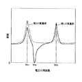
ところで、このような質量部21、22、23よりなる振動系(2自由度振動系)では、第1の質量部21、22および第2の質量部23の振幅(振れ角)と、印加する交流電圧の周波数との間に、図5に示すような周波数特性が存在している。
すなわち、かかる振動系は、第1の質量部21、22の振幅と、第2の質量部23の振幅とが大きくなる2つの共振周波数fm1[kHz]、fm3[kHz](ただし、fm1<fm3)と、第1の質量部21、22の振幅がほぼ0となる、1つの反共振周波数fm2[kHz]とを有している。
By the way, in such a vibration system (two-degree-of-freedom vibration system) composed of the
That is, the vibration system includes two resonance frequencies fm 1 [kHz] and fm 3 [kHz] (however, fm) in which the amplitude of the
この振動系では、第1の質量部21、22と圧電体32との間に印加する交流電圧の周波数Fが、2つの共振周波数のうち低いもの、すなわち、fm1とほぼ等しくなるように設定するのが好ましい。これにより、第1の質量部21、22の振幅を抑制しつつ、第2の質量部23の振れ角(回転角度)を大きくすることができる。
なお、本明細書中では、F[kHz]とfm1[kHz]とがほぼ等しいとは、(fm1−1)≦F≦(fm1+1)の条件を満足することを意味する。
In this vibration system, the frequency F of the alternating voltage applied between the
In this specification, F [kHz] and fm 1 [kHz] being substantially equal means that the condition of (fm 1 −1) ≦ F ≦ (fm 1 +1) is satisfied.
第1の質量部21、22の平均厚さは、それぞれ、1〜1500μmであるのが好ましく、10〜300μmであるのがより好ましい。
第2の質量部23の平均厚さは、1〜1500μmであるのが好ましく、10〜300μmであるのがより好ましい。
第1の弾性連結部25のばね定数k1は、1×10⁻⁴〜1×10⁴Nm/radであるのが好ましく、1×10−2〜1×103Nm/radであるのがより好ましく、1×10−1〜1×102Nm/radであるのがさらに好ましい。これにより、第2の質量部23の回転角度(振れ角)をより大きくすることができる。
The average thicknesses of the
The average thickness of the second
The spring constant k 1 of the first elastic connecting
一方、第2の弾性連結部26のばね定数k2は、1×10⁻⁴〜1×10⁴Nm/radであるのが好ましく、1×10−2〜1×103Nm/radであるのがより好ましく、1×10−1〜1×102Nm/radであるのがさらに好ましい。これにより、第1の質量部21、22の振れ角を抑制しつつ、第2の質量部23の振れ角をより大きくすることができる。
また、第1の弾性連結部25のばね定数k1と第2の弾性連結部26のばね定数をk2とは、k1>k2なる関係を満足するのが好ましい。これにより、第1の質量部21、22の振れ角を抑制しつつ、第2の質量部23の回転角度(振れ角)をより大きくすることができる。
On the other hand, the spring constant k 2 of the second
Further, the spring constant k 1 of the first elastic connecting
さらに、第1の質量部21、22の慣性モーメントをJ1とし、第2の質量部23の慣性モーメントをJ2としたとき、J1とJ2とは、J1≦J2なる関係を満足することが好ましく、J1<J2なる関係を満足することがより好ましい。これにより、第1の質量部21、22の振れ角を抑制しつつ、第2の質量部23の回転角度(振れ角)をより大きくすることができる。
Furthermore, the moment of inertia of the first
ところで、第1の質量部21、22と第1の弾性連結部25、25とからなる第1の振動系の固有振動数ω1は、第1の質量部21、22の慣性モーメントJ1と、第1の弾性連結部25のばね定数k1とにより、ω1=(k1/J1)1/2によって与えられる。一方、第2の質量部23と第2の弾性連結部26、26とからなる第2の振動系の固有振動数ω2は、第2の質量部23の慣性モーメントJ2と、第2の弾性連結部26のばね定数k2とにより、ω2=(k2/J2)1/2によって与えられる。
Incidentally, the natural frequency ω 1 of the first vibration system composed of the
このようにして求められる第1の振動系の固有振動数ω1と第2の振動系の固有振動数ω2とは、ω1>ω2なる関係を満足するのが好ましい。これにより、第1の質量部21、22の振れ角を抑制しつつ、第2の質量部23の回転角度(振れ角)をより大きくすることができる。
なお、本実施形態の振動系は、一対の第1の弾性連結部25および一対の第2の弾性連結部26のうち少なくとも1つの内部にピエゾ抵抗素子を設けることにより、例えば、回転角度および回転周波数を検出したりすることができ、また、その検出結果を、第2の質量部23の姿勢の制御に利用することができる。
It is preferable that the natural frequency ω 1 of the first vibration system and the natural frequency ω 2 of the second vibration system obtained in this way satisfy the relationship ω 1 > ω 2 . Thereby, it is possible to increase the rotation angle (deflection angle) of the
Note that the vibration system according to the present embodiment is provided with a piezoresistive element in at least one of the pair of first
ここで、各接合膜81、82について説明する。なお、本実施形態では、接合膜81の構成と接合膜82の構成は共通であるため、以下では、接合膜81を代表に説明する。
図6は、本実施形態にかかるアクチュエータが備える接合膜のエネルギー付与前の状態を示す部分拡大図、図7は、本実施形態にかかるアクチュエータが備える接合膜のエネルギー付与後の状態を示す部分拡大図である。
Here, the
FIG. 6 is a partially enlarged view showing a state before applying energy of the bonding film included in the actuator according to the present embodiment, and FIG. 7 is a partial enlarged view showing a state after applying energy of the bonding film included in the actuator according to the present embodiment. FIG.
接合膜81のエネルギーを付与する前の状態は、図6に示すように、シロキサン(Si−O)結合302を含み、ランダムな原子構造を有するSi骨格301と、このSi骨格301に結合する脱離基303とを含むものである。
そして、この接合膜81にエネルギーを付与すると、図7に示すように、一部の脱離基303がSi骨格301から脱離し、代わりに活性手304が生じる。これにより、接合膜81の表面に接着性が発現する。このようにして接着性が発現した接合膜81により、基体2と支持体3との間が接合されている。
このような接合膜81は、薄くても十分な接合強度が得られるので、接合される各部の間に剥離等の不具合が生じるのを確実に防止することができる。
As shown in FIG. 6, the state before applying energy to the
When energy is applied to the
Even if such a
また、接合膜81は、気相成膜法のような方法で作製することができるので、厚さを厳密に制御することができ、接合される各部(基体2と支持体3)の間隙(ギャップ)の寸法精度を高めることができる。
また、接合膜81は、通気性が低く、接合される各部に対する密着性も高い。このため、接合膜81を介して接合された接合箇所は、優れた気密性を有することとなり、凹部31および凹部28、29で構成される気密空間の気密性を高めることができる。したがって、気密空間内への外気や異物の侵入が防止されることとなり、外気やそれに含まれる水分等によって、気密空間内に配された2自由度振動系や圧電アクチュエータが変質・劣化したり、異物によって、2自由度振動系の振動が妨げられたりするのを防止することができる。
したがって、気密空間内を減圧したり、所定のガスを充填したことにより、これらの減圧状態やガス充填状態を、長期にわたって安定的に保持することができる。
In addition, since the
Further, the
Therefore, the reduced pressure state or the gas filling state can be stably maintained for a long time by reducing the pressure in the airtight space or filling a predetermined gas.
また、接合膜81は、化学的に安定なSi骨格301の作用により、耐熱性に優れている。このため、アクチュエータ1が高温下に曝されたとしても、接合膜81に変質・劣化が生じ難い。したがって、接合箇所に剥離等の不具合が生じるのを確実に防止することができる。
また、このような接合膜81は、流動性を有しない固体状のものである。このため、従来の流動性を有する液状または粘液状の接着剤に比べて、接着層(接合膜81)の厚さや形状がほとんど変化しない。このため、接合膜81を用いて製造されたアクチュエータ1の寸法精度は、従来に比べて格段に高いものとなる。これにより、例えば、基体2と支持体3との間の平行度を長期にわたって一定に維持することができ、長期信頼性の高いアクチュエータ1が得られる。
また、はみ出した接着剤を除去するといった手間を省略することができる。
さらに、接着剤の硬化に要する時間が不要になるため、短時間で強固な接合を可能にするものである。
Further, the
Further, such a
Moreover, the trouble of removing the protruding adhesive can be omitted.
Furthermore, since the time required for curing of the adhesive is not required, strong bonding can be achieved in a short time.
このような接合膜81としては、特に、接合膜81を構成する全原子からH原子を除いた原子のうち、Si原子の含有率とO原子の含有率の合計が、10〜90原子%程度であるのが好ましく、20〜80原子%程度であるのがより好ましい。Si原子とO原子とが、前記範囲の含有率で含まれていれば、接合膜81は、Si原子とO原子とが強固なネットワークを形成し、接合膜81自体がより強固なものとなる。したがって、かかる接合膜81によれば、接合箇所の接合強度をより高めることができる。
As such a
また、接合膜81中のSi原子とO原子の存在比は、3:7〜7:3程度であるのが好ましく、4:6〜6:4程度であるのがより好ましい。Si原子とO原子の存在比を前記範囲内になるよう設定することにより、接合膜81の安定性が高くなり、各部をより強固に接合することができるようになる。
なお、接合膜81中のSi骨格301の結晶化度は、45%以下であるのが好ましく、40%以下であるのがより好ましい。これにより、Si骨格301は十分にランダムな原子構造を含むものとなる。このため、前述した化学的安定性、耐熱性等のSi骨格301の特性が顕在化し、接合膜81の寸法精度および接着性がより優れたものとなる。
The abundance ratio of Si atoms to O atoms in the
The crystallinity of the
また、Si骨格301に結合する脱離基303は、前述したように、Si骨格301から脱離することによって、接合膜81に活性手304を生じさせるよう振る舞うものである。したがって、脱離基303には、エネルギーを付与されることによって、比較的簡単に、かつ均一に脱離するものの、エネルギーが付与されないときには、脱離しないようSi骨格301に確実に結合しているものである必要がある。
Further, the leaving
かかる観点から、脱離基303には、H原子、B原子、C原子、N原子、O原子、P原子、S原子およびハロゲン系原子、またはこれらの各原子を含み、これらの各原子がSi骨格301に結合するよう配置された原子団からなる群から選択される少なくとも1種で構成されたものが好ましく用いられる。かかる脱離基303は、エネルギーの付与による結合/脱離の選択性に比較的優れている。このため、このような脱離基303は、上記のような必要性を十分に満足し得るものとなり、接合膜81の接着性をより高度なものとすることができる。
From this point of view, the leaving
なお、上記のような各原子がSi骨格301に結合するよう配置された原子団(基)としては、例えば、メチル基、エチル基のようなアルキル基、ビニル基、アリル基のようなアルケニル基、アルデヒド基、ケトン基、カルボキシル基、アミノ基、アミド基、ニトロ基、ハロゲン化アルキル基、メルカプト基、スルホン酸基、シアノ基、イソシアネート基等が挙げられる。
これらの各基の中でも、脱離基303は、特にアルキル基であるのが好ましい。アルキル基は化学的な安定性が高いため、アルキル基を含む接合膜81は、耐候性および耐薬品性に優れたものとなる。
Examples of the atomic group (group) arranged so that each atom as described above is bonded to the
Among these groups, the leaving
このような特徴を有する接合膜81の構成材料としては、例えば、ポリオルガノシロキサンのようなシロキサン結合を含む重合物等が挙げられる。
ポリオルガノシロキサンで構成された接合膜81は、それ自体が優れた機械的特性を有している。また、多くの材料に対して特に優れた接着性を示すものである。したがって、ポリオルガノシロキサンで構成された接合膜81は、接合される各部の間をより強固に接合することができる。
また、ポリオルガノシロキサンは、通常、撥水性(非接着性)を示すが、エネルギーを付与されることにより、容易に有機基を脱離させることができ、親水性に変化し、接着性を発現するが、この非接着性と接着性との制御を容易かつ確実に行えるという利点を有する。
Examples of the constituent material of the
The
Polyorganosiloxane usually exhibits water repellency (non-adhesiveness), but when given energy, it can easily desorb organic groups, changes to hydrophilicity, and exhibits adhesiveness. However, there is an advantage that the non-adhesiveness and the adhesiveness can be controlled easily and reliably.
また、ポリオルガノシロキサンの中でも、特に、オクタメチルトリシロキサンの重合物を主成分とするものが好ましい。オクタメチルトリシロキサンの重合物を主成分とする接合膜81は、接着性に特に優れることから、本発明の封止型デバイスに対して特に好適に適用できるものである。また、オクタメチルトリシロキサンを主成分とする原料は、常温で液状をなし、適度な粘度を有するため、取り扱いが容易であるという利点もある。
また、接合膜81の平均厚さは、1〜1000nm程度であるのが好ましく、2〜800nm程度であるのがより好ましい。接合膜81の平均厚さを前記範囲内とすることにより、接合される各部の間の寸法精度や透明性(透光性)が著しく低下するのを防止しつつ、これらをより強固に接合することができる。
Further, among polyorganosiloxanes, those mainly composed of a polymer of octamethyltrisiloxane are preferred. Since the
The average thickness of the
すなわち、接合膜81の平均厚さが前記下限値を下回った場合は、十分な接合強度が得られないおそれがある。一方、接合膜81の平均厚さが前記上限値を上回った場合は、アクチュエータ1の寸法精度や透光性(透明性)が著しく低下するおそれがある。その結果、特に図2に示す接合膜82のように、それ自体を光が透過するような構成のアクチュエータでは、接合膜82によって光が吸収されてしまうおそれがある。
That is, when the average thickness of the
さらに、接合膜81の平均厚さが前記範囲内であれば、接合膜81にある程度の形状追従性が確保される。このため、例えば、支持体3の接合面(接合膜81に隣接する面)に凹凸が存在している場合でも、その凹凸の高さにもよるが、凹凸の形状に追従するように接合膜81を被着させることができる。その結果、接合膜81は、凹凸を吸収して、その表面に生じる凹凸の高さを緩和することができる。そして、接合膜81を備える支持体3に対して基体2を貼り合わせた際に、これらの密着性をより高めることができる。
なお、上記のような形状追従性の程度は、接合膜81の厚さが厚いほど顕著になる。したがって、形状追従性を十分に確保するためには、接合膜81の厚さをできるだけ厚くすればよい。
Furthermore, if the average thickness of the
Note that the degree of the shape followability as described above becomes more prominent as the
次に、本発明の封止型デバイスの製造方法の一例として、図8ないし図11に基づいて、前述したアクチュエータ1の製造方法を説明する。
図8〜図11は、それぞれ、第1実施形態にかかるアクチュエータの製造方法を説明するための図(縦断面図)である。なお、以下では、説明の便宜上、図8〜図11中の上側を「上」、下側を「下」と言う。
Next, as an example of the manufacturing method of the sealed device of the present invention, the manufacturing method of the
8 to 11 are views (longitudinal sectional views) for explaining the manufacturing method of the actuator according to the first embodiment. In the following, for convenience of explanation, the upper side in FIGS. 8 to 11 is referred to as “upper” and the lower side is referred to as “lower”.
本実施形態にかかるアクチュエータ1の製造方法は、[1]接合膜81を備える支持体3(第1の構造体)と、第1の質量部23を有する基体2(第2の構造体)と、接合膜82を備える支持体4(第1の構造体)とを用意する準備工程と、[2]各接合膜81、82にそれぞれエネルギーを付与するエネルギー付与工程と、[3]減圧下またはガス存在下において、支持体3、基体2および支持体4をこの順で積層する接合工程とを有する。以下、各工程について順次説明する。
The manufacturing method of the
[1]準備工程
[1−1]基体2の製造
まず、図8(a)に示すように、基体2を形成するための基板5を用意する。
基板5の構成材料は、前述した基体2の構成材料と同様である。
そして、図8(b)に示すように、基板5の両方の面に、フォトレジストを塗布し、露光、現像を行う。これにより、図8(b)に示すように、支持部24の形状に対応するように、レジストマスク6を形成する。
[1] Preparation Step [1-1] Manufacture of
The constituent material of the
And as shown in FIG.8 (b), a photoresist is apply | coated to both surfaces of the board |
次に、このレジストマスク6を介して、基板5の両方の面をエッチングした後、レジストマスク6を除去する。これにより、図8(c)に示すように、支持部24に対応する部分以外の領域に凹部51が形成される。なお、その際、エッチングは、基板5の両面に対して、同時に行ってもよいし、片面ずつ行ってもよい。基板5に対し片面ずつエッチングを行う場合には、後述の金属マスク7を形成する側の一方の面のエッチングと、他方の面のエッチングとの先後はどちらでも構わない。
Next, after etching both surfaces of the
エッチング方法としては、例えば、プラズマエッチング、リアクティブイオンエッチング、ビームエッチング、光アシストエッチング等の物理的エッチング法、ウェットエッチング等の化学的エッチング法等のうちの1種または2種以上を組み合わせて用いることができる。なお、以下の各工程におけるエッチングにおいても、同様の方法を用いることができる。 As an etching method, for example, one or more of physical etching methods such as plasma etching, reactive ion etching, beam etching, and light-assisted etching, and chemical etching methods such as wet etching are used in combination. be able to. Note that the same method can be used for etching in the following steps.
次に、基板5の一方の面に、図8(d)に示すように、支持部24と各質量部21、22、23との形状に対応するように、例えば、アルミニウム等により金属マスク7を形成する。
次に、金属マスク7を介して、基板5の一方の面側を、前記凹部51に対応する部分が貫通するまでエッチングする。
Next, on one surface of the
Next, the one surface side of the
そして、金属マスク7を除去した後、図8(e)に示すように、第2の質量部23上に金属膜を成膜し、光反射部231を形成する。
なお、ここで、基板5をエッチングした後、金属マスク7は除去してもよく、除去せずに残存させてもよい。金属マスク7を除去しない場合、第2の質量部23上に残存した金属マスク7は光反射部231として用いることができる。
Then, after removing the
Here, after the
金属マスク7の形成方法(金属膜の成膜方法)としては、特に限定されないが、例えば、真空蒸着、スパッタリング(低温スパッタリング)、イオンプレーティング等の乾式メッキ法、電解メッキ、無電解メッキ等の湿式メッキ法、溶射法、金属箔の接合等が挙げられる。なお、以下の各工程における金属膜の成膜においても、同様の方法を用いることができる。
以上の工程により、図8(e)に示すように、各質量部21、22、23および支持部24が一体的に形成された構造体、すなわち基体2が得られる。
A method for forming the metal mask 7 (a method for forming a metal film) is not particularly limited, and examples thereof include dry plating methods such as vacuum deposition, sputtering (low temperature sputtering), and ion plating, electrolytic plating, and electroless plating. Examples include a wet plating method, a thermal spraying method, and a metal foil bonding. Note that the same method can also be used for forming a metal film in the following steps.
Through the above steps, as shown in FIG. 8E, a structure in which the
[1−2]支持体3の製造
次に、図9(a)に示すように、支持体3を形成するためのガラス基板である基板9を用意する。なお、基板9として、シリコン基板または金属基板を用いることもできる。
そして、基板9の一方の面に、凹部31を形成する領域を除いた部分に対応するように、例えば、アルミニウム等により金属マスク(図示せず)を形成する。
次に、この金属マスクを介して、基板9の一方の面側をエッチングした後、金属マスクを除去する。これにより、図9(b)に示すように、凹部31が形成された支持体3が得られる。
[1-2] Production of
Then, a metal mask (not shown) is formed on one surface of the
Next, after etching one surface side of the
[1−3]接合膜81の製造
次に、支持体3上に、図9(c)に示すように、接合膜81を形成する。
以下、支持体3上に接合膜81を形成する方法について説明する。
このような接合膜81は、いかなる方法で作製されたものでもよく、プラズマ重合法、CVD法、PVD法のような各種気相成膜法や、各種液相成膜法等により作製した膜にエネルギーを付与することによって作製することができるが、これらの中でも、エネルギー付与前の膜として、プラズマ重合法により作製された膜を用いるのが好ましい。プラズマ重合法によれば、最終的に、緻密で均質な接合膜81を効率よく作製することができる。これにより、プラズマ重合法で作製された接合膜81は、接合される各部の間を特に強固に、かつ高い気密性を有しつつ接合することができる。また、プラズマ重合法で作製され、エネルギーが付与される前の接合膜81は、エネルギーが付与されて活性化された状態を比較的長時間にわたって維持することができる。このため、アクチュエータ1の製造過程の簡素化、効率化を図ることができる。
[1-3] Production of
Hereinafter, a method for forming the
Such a
ここでは、接合膜81をプラズマ重合法にて形成する方法について詳述するが、接合膜81の形成方法を説明するのに先立って、接合膜81を作製する際に用いるプラズマ重合装置について説明し、その後、接合膜81の形成方法について説明する。
図12は、プラズマ重合装置を模式的に示す縦断面図である。なお、以下の説明では、図12中の上側を「上」、下側を「下」と言う。
Here, a method for forming the
FIG. 12 is a longitudinal sectional view schematically showing a plasma polymerization apparatus. In the following description, the upper side in FIG. 12 is referred to as “upper” and the lower side is referred to as “lower”.
図12に示すプラズマ重合装置100は、チャンバー101と、支持体3を支持する第1の電極130と、第2の電極140と、各電極130、140間に高周波電圧を印加する電源回路180と、チャンバー101内にガスを供給するガス供給部190と、チャンバー101内のガスを排気する排気ポンプ170とを備えている。これらの各部のうち、第1の電極130および第2の電極140がチャンバー101内に設けられている。以下、各部について詳細に説明する。
A
チャンバー101は、内部の気密を保持し得る容器であり、内部を減圧(真空)状態にして使用されるため、内部と外部との圧力差に耐え得る耐圧性能を有するものとされる。
図12に示すチャンバー101は、軸線が水平方向に沿って配置されたほぼ円筒形をなすチャンバー本体と、チャンバー本体の左側開口部を封止する円形の側壁と、右側開口部を封止する円形の側壁とで構成されている。
The
The
チャンバー101の上方には供給口103が、下方には排気口104が、それぞれ設けられている。そして、供給口103にはガス供給部190が接続され、排気口104には排気ポンプ170が接続されている。
なお、本実施形態では、チャンバー101は、導電性の高い金属材料で構成されており、接地線102を介して電気的に接地されている。
A
In this embodiment, the
第1の電極130は、板状をなしており、支持体3を支持している。
この第1の電極130は、チャンバー101の側壁の内壁面に、鉛直方向に沿って設けられており、これにより、第1の電極130は、チャンバー101を介して電気的に接地されている。なお、第1の電極130は、図12に示すように、チャンバー本体と同心状に設けられている。
The
The
第1の電極130の支持体3を支持する面には、静電チャック(吸着機構)139が設けられている。
この静電チャック139により、図12に示すように、支持体3を鉛直方向に沿って支持することができる。また、支持体3に多少の反りがあっても、静電チャック139に吸着させることにより、その反りを矯正した状態で支持体3をプラズマ処理に供することができる。
An electrostatic chuck (suction mechanism) 139 is provided on the surface of the
As shown in FIG. 12, the
第2の電極140は、支持体3を介して、第1の電極130と対向して設けられている。なお、第2の電極140は、チャンバー101の側壁の内壁面から離間した(絶縁された)状態で設けられている。
この第2の電極140には、配線184を介して高周波電源182が接続されている。また、配線184の途中には、マッチングボックス(整合器)183が設けられている。これらの配線184、高周波電源182およびマッチングボックス183により、電源回路180が構成されている。
このような電源回路180によれば、第1の電極130は接地されているので、第1の電極130と第2の電極140との間に高周波電圧が印加される。これにより、第1の電極130と第2の電極140との間隙には、高い周波数で向きが反転する電界が誘起される。
The
A high
According to such a
ガス供給部190は、チャンバー101内に所定のガスを供給するものである。
図12に示すガス供給部190は、液状の膜材料(原料液)を貯留する貯液部191と、液状の膜材料を気化してガス状に変化させる気化装置192と、キャリアガスを貯留するガスボンベ193とを有している。また、これらの各部とチャンバー101の供給口103とが、それぞれ配管194で接続されており、ガス状の膜材料(原料ガス)とキャリアガスとの混合ガスを、供給口103からチャンバー101内に供給するように構成されている。
The
A
貯液部191に貯留される液状の膜材料は、プラズマ重合装置100により、重合して支持体3の表面に重合膜を形成する原材料となるものである。
このような液状の膜材料は、気化装置192により気化され、ガス状の膜材料(原料ガス)となってチャンバー101内に供給される。なお、原料ガスについては、後に詳述する。
The liquid film material stored in the
Such a liquid film material is vaporized by the
ガスボンベ193に貯留されるキャリアガスは、電界の作用により放電し、およびこの放電を維持するために導入するガスである。このようなキャリアガスとしては、例えば、Arガス、Heガス等が挙げられる。
また、チャンバー101内の供給口103の近傍には、拡散板195が設けられている。
拡散板195は、チャンバー101内に供給される混合ガスの拡散を促進する機能を有する。これにより、混合ガスは、チャンバー101内に、ほぼ均一の濃度で分散することができる。
The carrier gas stored in the
A
The
排気ポンプ170は、チャンバー101内を排気するものであり、例えば、油回転ポンプ、ターボ分子ポンプ等で構成される。このようにチャンバー101内を排気して減圧することにより、ガスを容易にプラズマ化することができる。また、大気雰囲気との接触による支持体3の汚染・酸化等を防止するとともに、プラズマ処理による反応生成物をチャンバー101内から効果的に除去することができる。
また、排気口104には、チャンバー101内の圧力を調整する圧力制御機構171が設けられている。これにより、チャンバー101内の圧力が、ガス供給部160の動作状況に応じて、適宜設定される。
The
The
次に、支持体3上に、このようなプラズマ重合装置100を用いて接合膜81を形成する方法について説明する。
まず、支持体3をプラズマ重合装置100のチャンバー101内に収納して封止状態とした後、排気ポンプ170の作動により、チャンバー101内を減圧状態とする。
次に、ガス供給部190を作動させ、チャンバー101内に原料ガスとキャリアガスの混合ガスを供給する。供給された混合ガスは、チャンバー101内に充填される。
Next, a method for forming the
First, the
Next, the
ここで、混合ガス中における原料ガスの占める割合(混合比)は、原料ガスやキャリアガスの種類や目的とする成膜速度等によって若干異なるが、例えば、混合ガス中の原料ガスの割合を20〜70%程度に設定するのが好ましく、30〜60%程度に設定するのがより好ましい。これにより、重合膜の形成(成膜)の条件の最適化を図ることができる。
また、供給するガスの流量は、ガスの種類や目的とする成膜速度、膜厚等によって適宜決定され、特に限定されるものではないが、通常は、原料ガスおよびキャリアガスの流量を、それぞれ、1〜100ccm程度に設定するのが好ましく、10〜60ccm程度に設定するのがより好ましい。
Here, the proportion (mixing ratio) of the raw material gas in the mixed gas is slightly different depending on the kind of the raw material gas and the carrier gas, the target film forming speed, and the like. It is preferable to set to about -70%, and it is more preferable to set to about 30-60%. As a result, it is possible to optimize the conditions for formation (film formation) of the polymer film.
Further, the flow rate of the gas to be supplied is appropriately determined depending on the type of gas, the target film formation rate, the film thickness, etc., and is not particularly limited, but usually the flow rates of the source gas and the carrier gas are respectively , Preferably about 1 to 100 ccm, more preferably about 10 to 60 ccm.
次いで、電源回路180を作動させ、一対の電極130、140間に高周波電圧を印加する。これにより、一対の電極130、140間に存在するガスの分子が電離し、プラズマが発生する。このプラズマのエネルギーにより原料ガス中の分子が重合し、重合物が支持体3上に付着・堆積する。これにより、図9(c)に示すように、支持体3上にプラズマ重合膜で構成された接合膜81が形成される。
Next, the
原料ガスとしては、例えば、メチルシロキサン、オクタメチルトリシロキサン、デカメチルテトラシロキサン、デカメチルシクロペンタシロキサン、オクタメチルシクロテトラシロキサン、メチルフェニルシロキサンのようなオルガノシロキサン等が挙げられる。
このような原料ガスを用いて得られるプラズマ重合膜、すなわち接合膜81は、これらの原料が重合してなるもの(重合物)、すなわちポリオルガノシロキサンで構成されることとなる。
Examples of the source gas include organosiloxanes such as methylsiloxane, octamethyltrisiloxane, decamethyltetrasiloxane, decamethylcyclopentasiloxane, octamethylcyclotetrasiloxane, and methylphenylsiloxane.
The plasma polymerized film obtained by using such a raw material gas, that is, the
プラズマ重合の際、一対の電極130、140間に印加する高周波の周波数は、特に限定されないが、1kHz〜100MHz程度であるのが好ましく、10〜60MHz程度であるのがより好ましい。
また、高周波の出力密度は、特に限定されないが、0.01〜10W/cm2程度であるのが好ましく、0.1〜1W/cm2程度であるのがより好ましい。
In the plasma polymerization, the frequency of the high frequency applied between the pair of
Further, the power density of the high frequency is not particularly limited, and is preferably about 0.01 to 10 / cm 2, more preferably about 0.1 to 1 W / cm 2.
また、成膜時のチャンバー101内の圧力は、133.3×10⁻⁵〜1333Pa(1×10⁻⁵〜10Torr)程度であるのが好ましく、133.3×10⁻⁴〜133.3Pa(1×10⁻⁴〜1Torr)程度であるのがより好ましい。
原料ガス流量は、0.5〜200sccm程度であるのが好ましく、1〜100sccm程度であるのがより好ましい。一方、キャリアガス流量は、5〜750sccm程度であるのが好ましく、10〜500sccm程度であるのがより好ましい。
Further, the pressure in the
The raw material gas flow rate is preferably about 0.5 to 200 sccm, and more preferably about 1 to 100 sccm. On the other hand, the carrier gas flow rate is preferably about 5 to 750 sccm, and more preferably about 10 to 500 sccm.
処理時間は、1〜10分程度であるのが好ましく、4〜7分程度であるのがより好ましい。なお、成膜される接合膜81の厚さは、主に、この処理時間に比例する。したがって、この処理時間を調整することのみで、接合膜81の厚さを容易に調整することができる。このため、支持体3と基体2との間の距離を厳密に制御することができる。
また、支持体3の温度は、25℃以上であるのが好ましく、25〜100℃程度であるのがより好ましい。
The treatment time is preferably about 1 to 10 minutes, more preferably about 4 to 7 minutes. Note that the thickness of the
Moreover, it is preferable that the temperature of the
以上のようにして、接合膜81を得ることができ、支持体(基材)3と接合膜81とで構成される第1の構造体が得られる。
なお、支持体3の上面のうち、部分的に接合膜81を形成する場合、例えば、その領域に対応する形状の窓部を有するマスクを用い、このマスク上から接合膜81を成膜するようにすればよい。
As described above, the
When the
[1−3]支持体4の準備
次に、ガラス基板で構成された支持体4を準備する。
[1−4]接合膜82の製造
次に、図10(a)に示すように、支持体4の下面に、接合膜81と同様にして接合膜82を形成する。これにより、支持体(基材)4と接合膜82とで構成される第1の構造体が得られる。
[1-3] Preparation of
[1-4] Production of
[2]エネルギー付与工程
[2−1]次に、支持体3上に形成した接合膜81に対してエネルギーを付与する。
エネルギーが付与されると、接合膜81では、図6に示す脱離基303がSi骨格301から脱離する。そして、脱離基303が脱離した後には、図7に示すように、接合膜81の表面および内部に活性手304が生じる。これにより、接合膜81の表面に、基体2との接着性が発現する。また、接合膜82においても同様に、基体2との接着性が発現する。
[2] Energy application step [2-1] Next, energy is applied to the
When energy is applied, the leaving
ここで、接合膜81に付与するエネルギーは、いかなる方法で付与されてもよく、例えば、(I)接合膜81にエネルギー線を照射する方法、(II)接合膜81を加熱する方法、(III)接合膜81に圧縮力を付与する(物理的エネルギーを付与する)方法が代表的に挙げられ、この他、プラズマに曝す(プラズマエネルギーを付与する)方法、オゾンガスに曝す(化学的エネルギーを付与する)方法等が挙げられる。
このうち、接合膜81にエネルギーを付与する方法として、特に、上記(I)、(II)、(III)の各方法のうち、少なくとも1つの方法を用いるのが好ましい。これらの方法は、接合膜81に対して比較的簡単に効率よくエネルギーを付与することができるので、エネルギー付与方法として好適である。
Here, the energy applied to the
Among these, as a method for applying energy to the
以下、上記(I)、(II)、(III)の各方法について詳述する。
(I)接合膜81にエネルギー線を照射する場合、エネルギー線としては、例えば、紫外線、レーザー光のような光、X線、γ線、電子線、イオンビームのような粒子線等、またはこれらのエネルギー線を組み合わせたものが挙げられる。
これらのエネルギー線の中でも、特に、波長126〜300nm程度の紫外線を用いるのが好ましい(図9(d)参照)。かかる紫外線によれば、付与されるエネルギー量が最適化されるので、接合膜81中のSi骨格301が必要以上に破壊されるのを防止しつつ、Si骨格301と脱離基303との間の結合を選択的に切断することができる。これにより、接合膜81の特性(機械的特性、化学的特性等)が低下するのを防止しつつ、接合膜81に接着性を発現させることができる。
また、紫外線によれば、広い範囲をムラなく短時間に処理することができるので、脱離基303の脱離を効率よく行わせることができる。さらに、紫外線には、例えば、UVランプ等の簡単な設備で発生させることができるという利点もある。
なお、紫外線の波長は、より好ましくは、126〜200nm程度とされる。
Hereinafter, the methods (I), (II), and (III) will be described in detail.
(I) In the case of irradiating the
Among these energy rays, it is particularly preferable to use ultraviolet rays having a wavelength of about 126 to 300 nm (see FIG. 9D). According to such ultraviolet rays, the amount of energy applied is optimized, so that the
In addition, since ultraviolet rays can be processed in a short time without unevenness, the leaving
The wavelength of the ultraviolet light is more preferably about 126 to 200 nm.
また、UVランプを用いる場合、その出力は、接合膜81の面積に応じて異なるが、1mW/cm2〜1W/cm2程度であるのが好ましく、5mW/cm2〜50mW/cm2程度であるのがより好ましい。なお、この場合、UVランプと接合膜81との離間距離は、3〜3000mm程度とするのが好ましく、10〜1000mm程度とするのがより好ましい。
In the case of using the UV lamp, the output may vary depending on the area of the
また、紫外線を照射する時間は、接合膜81の表面付近の脱離基303を脱離し得る程度の時間、すなわち、接合膜81の内部の脱離基303を多量に脱離させない程度の時間とするのが好ましい。具体的には、紫外線の光量、接合膜81の構成材料等に応じて若干異なるものの、0.5〜30分程度であるのが好ましく、1〜10分程度であるのがより好ましい。
In addition, the time of irradiation with ultraviolet rays is a time that allows the leaving
また、紫外線は、時間的に連続して照射されてもよいが、間欠的(パルス状)に照射されてもよい。
一方、レーザー光としては、例えば、エキシマレーザー(フェムト秒レーザー)、Nd−YAGレーザー、Arレーザー、CO2レーザー、He−Neレーザー等が挙げられる。
Moreover, although an ultraviolet-ray may be irradiated continuously in time, you may irradiate intermittently (pulse form).
On the other hand, examples of the laser light include an excimer laser (femtosecond laser), an Nd-YAG laser, an Ar laser, a CO 2 laser, and a He—Ne laser.
また、接合膜81に対するエネルギー線の照射は、いかなる雰囲気中で行うようにしてもよく、具体的には、大気、酸素のような酸化性ガス雰囲気、水素のような還元性ガス雰囲気、窒素、アルゴンのような不活性ガス雰囲気、またはこれらの雰囲気を減圧した減圧(真空)雰囲気等が挙げられるが、特に大気雰囲気中で行うのが好ましい。これにより、雰囲気を制御することに手間やコストをかける必要がなくなり、エネルギー線の照射をより簡単に行うことができる。
Further, the irradiation of the energy beam to the
このように、エネルギー線を照射する方法によれば、接合膜81に対して選択的にエネルギーを付与することが容易に行えるため、例えば、エネルギーの付与による支持体3の変質・劣化を防止することができる。
また、エネルギー線を照射する方法によれば、付与するエネルギーの大きさを、精度よく簡単に調整することができる。このため、接合膜81から脱離する脱離基303の脱離量を調整することが可能となる。このように脱離基303の脱離量を調整することにより、接合膜81と基体2の間の接合強度を容易に制御することができる。
As described above, according to the method of irradiating the energy beam, it is possible to easily apply energy selectively to the
Moreover, according to the method of irradiating energy rays, the magnitude of energy to be applied can be easily adjusted with high accuracy. For this reason, it is possible to adjust the desorption amount of the leaving
すなわち、脱離基303の脱離量を多くすることにより、接合膜81の表面および内部に、より多くの活性手が生じるため、接合膜81に発現する接着性をより高めることができる。一方、脱離基303の脱離量を少なくすることにより、接合膜81の表面および内部に生じる活性手を少なくし、接合膜81に発現する接着性を抑えることができる。
なお、付与するエネルギーの大きさを調整するためには、例えば、エネルギー線の種類、エネルギー線の出力、エネルギー線の照射時間等の条件を調整すればよい。
さらに、エネルギー線を照射する方法によれば、短時間で大きなエネルギーを付与することができるので、エネルギーの付与をより効率よく行うことができる。
That is, by increasing the amount of elimination of the leaving
In addition, in order to adjust the magnitude | size of the energy to provide, what is necessary is just to adjust conditions, such as the kind of energy beam, the output of an energy beam, the irradiation time of an energy beam.
Furthermore, according to the method of irradiating energy rays, a large amount of energy can be applied in a short time, so that the energy can be applied more efficiently.
(II)接合膜81を加熱する場合(図示せず)、加熱温度を25〜100℃程度に設定するのが好ましく、50〜100℃程度に設定するのがより好ましい。かかる範囲の温度で加熱すれば、支持体3等が熱によって変質・劣化するのを確実に防止しつつ、接合膜81を確実に活性化させることができる。
また、加熱時間は、接合膜81の分子結合を切断し得る程度の時間であればよく、具体的には、加熱温度が前記範囲内であれば、1〜30分程度であるのが好ましい。
(II) When the
Further, the heating time may be a time that can break the molecular bond of the
また、接合膜81は、いかなる方法で加熱されてもよいが、例えば、ヒータを用いる方法、赤外線を照射する方法、火炎に接触させる方法等の各種加熱方法で加熱することができる。
なお、接合される部材間の熱膨張率がほぼ等しい場合には、上記のような条件で接合膜81を加熱すればよいが、これらの熱膨張率が互いに異なっている場合には、後に詳述するが、できるだけ低温下で接合を行うのが好ましい。接合を低温下で行うことにより、接合界面に発生する熱応力のさらなる低減を図ることができる。
The
When the thermal expansion coefficients between the members to be bonded are substantially equal, the
(III)接合膜81に圧縮力を付与する場合(図示せず)、0.2〜10MPa程度の圧力を付与するのが好ましく、1〜5MPa程度の圧力を付与するのがより好ましい。これにより、圧力が高すぎて支持体3に損傷等が生じるのを防止しつつ、単に圧縮力を付与することのみで、接合膜81に対して適度なエネルギーを簡単に付与することができ、接合膜81に十分な接着性が発現する。
また、圧縮力を付与する時間は、特に限定されないが、10秒〜30分程度であるのが好ましい。なお、圧縮力を付与する時間は、圧縮力の大きさに応じて適宜変更すればよい。具体的には、圧縮力の大きさが大きいほど、圧縮力を付与する時間を短くすることができる。
(III) When compressive force is applied to the bonding film 81 (not shown), it is preferable to apply a pressure of about 0.2 to 10 MPa, and it is more preferable to apply a pressure of about 1 to 5 MPa. Thereby, it is possible to easily apply an appropriate energy to the
The time for applying the compressive force is not particularly limited, but is preferably about 10 seconds to 30 minutes. In addition, what is necessary is just to change suitably the time which provides compression force according to the magnitude | size of compression force. Specifically, the time for applying the compressive force can be shortened as the compressive force increases.
以上のような(I)、(II)、(III)の各方法により、接合膜81にエネルギーを付与することができる。
なお、接合膜81の全面にエネルギーを付与するようにしてもよいが、一部の領域のみに付与するようにしてもよい。このようにすれば、接合膜81の接着性が発現する領域を制御することができ、この領域の面積・形状等を適宜調整することによって、接合界面に発生する応力の局所集中を緩和することができる。これにより、例えば、接合される部材間の熱膨張率差が大きい場合でも、これらを確実に接合することができる。
Energy can be imparted to the
Note that energy may be applied to the entire surface of the
ここで、前述したように、エネルギーが付与される前の状態の接合膜81は、図6に示すように、Si骨格301と脱離基303とを有している。かかる接合膜81にエネルギーが付与されると、脱離基303(本実施形態では、メチル基)がSi骨格301から脱離する。これにより、図7に示すように、接合膜81の表面35に活性手304が生じ、活性化される。その結果、接合膜81の表面に接着性が発現する。
Here, as described above, the
ここで、接合膜81を「活性化させる」とは、接合膜81の表面35および内部の脱離基303が脱離して、Si骨格301において終端化されていない結合手(以下、「未結合手」または「ダングリングボンド」とも言う。)が生じた状態や、この未結合手が水酸基(OH基)によって終端化された状態、または、これらの状態が混在した状態のことを言う。
Here, “activate” the
したがって、活性手304とは、未結合手(ダングリングボンド)、または未結合手が水酸基によって終端化されたもののことを言う。このような活性手304によれば、被着体に対して、特に強固な接合が可能となる。
なお、後者の状態(未結合手が水酸基によって終端化された状態)は、例えば、接合膜81に対して大気雰囲気中でエネルギー線を照射することにより、大気中の水分が未結合手を終端化することによって、容易に生成することができる。
Therefore, the
The latter state (state in which dangling bonds are terminated by a hydroxyl group) is obtained by, for example, irradiating the
次に、支持体3に形成された接合膜81上に、強誘電体材料を主材料として構成された圧電体32を形成する。
この圧電体32は、支持体3の凹部31が形成された面側に、強誘電体材料を主材料として構成された強誘電体膜を成膜し、この強誘電体膜に対し、圧電体32の形状に対応するマスクを介してエッチングを行った後、マスクを除去することにより形成することができる。
Next, a
In the
強誘電体膜の形成方法としては、特に限定されず、例えば、真空蒸着法、スパッタリング法(低温スパッタリング)、イオンプレーティング等のような物理的気相堆積法(PVD法)、プラズマCVD法、熱CVD法、レーザーCVD法のような化学気相堆積法(CVD法)、電解メッキ、浸漬メッキ、無電解メッキ等の湿式メッキ法、スピンコート法、溶液霧化堆積法(LSMCD法)などの溶液塗布法、スクリーン印刷法、インクジェット法などの各種印刷法、膜の接合等により形成することができる。
なお、圧電体32は、支持体3上に載置するだけでも構わない。
The method for forming the ferroelectric film is not particularly limited. For example, a physical vapor deposition method (PVD method) such as a vacuum deposition method, a sputtering method (low temperature sputtering), an ion plating method, a plasma CVD method, Chemical vapor deposition methods (CVD methods) such as thermal CVD methods, laser CVD methods, wet plating methods such as electrolytic plating, immersion plating, electroless plating, spin coating methods, solution atomization deposition methods (LSMCD methods), etc. It can be formed by various coating methods such as a solution coating method, a screen printing method, and an ink jet method, film bonding, and the like.
Note that the
また、圧電体32は、図9(e)に示すように、接合膜81を介して支持体3に接合されていてもよい。これにより、圧電体32と支持体3とを強固に接合することができる。また、接合膜81は、その厚さを厳密に制御することができるため、圧電体32と支持体3との間の離間距離の精度をより高めることができる。その結果、圧電体32を第1の質量部21、22に対して設計通りに作用させることができる。
[2−2]次に、接合膜81と同様にして、図10(b)に示すように、支持体4の下面に形成した接合膜82に対してエネルギーを付与する。
エネルギーが付与されると、接合膜82の表面に、基体2との接着性が発現する。
In addition, the
[2-2] Next, in the same manner as the
When energy is applied, adhesiveness with the
[3]接合工程
[3−1]次に、前記準備工程で作製した基体2を用意する。そして、図10(c)に示すように、接着性が発現してなる接合膜81と基体2とが密着するように、支持体3と基体2とを貼り合わせる。これにより、図10(d)に示すように、支持体3と基体2とが、接合膜81を介して接合(接着)される。
[3] Joining process [3-1] Next, the
ここで、上記のようにして接合される基体2と支持体3の各熱膨張率は、ほぼ等しいのが好ましい。基体2と支持体3の各熱膨張率がほぼ等しければ、これらを貼り合せた際に、その接合界面に熱膨張に伴う応力が発生し難くなる。その結果、最終的に得られるアクチュエータ1において、剥離等の不具合が発生するのを確実に防止することができる。
また、基体2と支持体3の各熱膨張率が互いに異なる場合でも、これらを貼り合わせる際の条件を以下のように最適化することにより、基体2と支持体3とを高い寸法精度で強固に接合することができる。
すなわち、基体2と支持体3の各熱膨張率が互いに異なっている場合には、できるだけ低温下で接合を行うのが好ましい。接合を低温下で行うことにより、接合界面に発生する熱応力のさらなる低減を図ることができる。
Here, it is preferable that the thermal expansion coefficients of the
Further, even when the thermal expansion coefficients of the
That is, when the thermal expansion coefficients of the
具体的には、基体2と支持体3との熱膨張率差にもよるが、基体2と支持体3の温度が25〜50℃程度である状態下で、これらを貼り合わせるのが好ましく、25〜40℃程度である状態下で貼り合わせるのがより好ましい。このような温度範囲であれば、基体2と支持体3との熱膨張率差がある程度大きくても、接合界面に発生する熱応力を十分に低減することができる。その結果、アクチュエータ1における反りや剥離等の発生を確実に防止することができる。
Specifically, although depending on the difference in thermal expansion coefficient between the
また、この場合、基体2と支持体3との間の熱膨張係数の差が、5×10⁻⁵/K以上あるような場合には、上記のようにして、できるだけ低温下で接合を行うことが特に推奨される。なお、接合膜81を用いることにより、上述したような低温下でも、基体2と支持体3とを強固に接合することができる。
また、基体2と支持体3は、互いに剛性が異なっているのが好ましい。これにより、基体2と支持体3とをより強固に接合することができる。
なお、支持体3の接合膜81を成膜する領域には、あらかじめ、接合膜81との密着性を高める表面処理を施すのが好ましい。これにより、支持体3と接合膜81との間の接合強度をより高めることができ、最終的には、基体2と支持体3との接合強度を高めることができる。
Further, in this case, when the difference in thermal expansion coefficient between the
The
In addition, it is preferable to perform a surface treatment for improving adhesion to the
かかる表面処理としては、例えば、スパッタリング処理、ブラスト処理のような物理的表面処理、酸素プラズマ、窒素プラズマ等を用いたプラズマ処理、コロナ放電処理、エッチング処理、電子線照射処理、紫外線照射処理、オゾン暴露処理のような化学的表面処理、または、これらを組み合わせた処理等が挙げられる。このような処理を施すことにより、支持体3の接合膜81を成膜する領域を清浄化するとともに、該領域を活性化させることができる。
Examples of the surface treatment include physical surface treatment such as sputtering treatment and blast treatment, plasma treatment using oxygen plasma, nitrogen plasma, etc., corona discharge treatment, etching treatment, electron beam irradiation treatment, ultraviolet irradiation treatment, ozone Examples include chemical surface treatment such as exposure treatment, or a combination of these. By performing such treatment, the region where the
また、これらの各表面処理の中でもプラズマ処理を用いることにより、接合膜81を形成するために、支持体3の表面を特に最適化することができる。
なお、表面処理を施す支持体3が、樹脂材料(高分子材料)で構成されている場合には、特に、コロナ放電処理、窒素プラズマ処理等が好適に用いられる。
また、支持体3の構成材料によっては、上記のような表面処理を施さなくても、接合膜81の接合強度が十分に高くなるものがある。このような効果が得られる支持体3の構成材料としては、例えば、各種金属系材料、各種シリコン系材料、各種ガラス系材料等を主材料とするものが挙げられる。
In addition, by using plasma treatment among these surface treatments, the surface of the
In addition, especially when the
Further, depending on the constituent material of the
このような材料で構成された支持体3は、その表面が酸化膜で覆われており、この酸化膜の表面には、比較的活性の高い水酸基が結合している。したがって、このような材料で構成された支持体3を用いると、上記のような表面処理を施さなくても、支持体3と接合膜81とを強固に密着させることができる。
なお、この場合、支持体3の全体が上記のような材料で構成されていなくてもよく、少なくとも接合膜81を成膜する領域の表面付近が上記のような材料で構成されていればよい。
The surface of the
In this case, the
さらに、支持体3の接合膜81を成膜する領域に、以下の基や物質を有する場合には、上記のような表面処理を施さなくても、支持体3と接合膜81との接合強度を十分に高くすることができる。
このような基や物質としては、例えば、水酸基、チオール基、カルボキシル基、アミノ基、ニトロ基、イミダゾール基のような官能基、ラジカル、開環分子、2重結合、3重結合のような不飽和結合、F、Cl、Br、Iのようなハロゲン、過酸化物からなる群から選択される少なくとも1つの基または物質が挙げられる。
また、このようなものを有する表面が得られるように、上述したような各種表面処理を適宜選択して行うのが好ましい。
Furthermore, in the case where the region where the
Examples of such groups and substances include functional groups such as hydroxyl groups, thiol groups, carboxyl groups, amino groups, nitro groups, and imidazole groups, radicals, ring-opened molecules, double bonds, and triple bonds. And at least one group or substance selected from the group consisting of a saturated bond, a halogen such as F, Cl, Br, and I, and a peroxide.
Further, it is preferable to appropriately select and perform various surface treatments as described above so that a surface having such a material can be obtained.
また、表面処理に代えて、支持体3の少なくとも接合膜81を成膜する領域には、あらかじめ、中間層を形成しておくのが好ましい。
この中間層は、いかなる機能を有するものであってもよく、例えば、接合膜81との密着性を高める機能、クッション性(緩衝機能)、応力集中を緩和する機能等を有するものが好ましい。このような中間層を介して支持体3上に接合膜81を成膜することにより、支持体3と接合膜81との接合強度を高め、信頼性の高い接合体、すなわちアクチュエータ1を得ることができる。
Further, instead of the surface treatment, it is preferable to form an intermediate layer in advance in at least a region of the
The intermediate layer may have any function, and for example, a layer having a function of improving adhesion to the
かかる中間層の構成材料としては、例えば、アルミニウム、チタンのような金属系材料、金属酸化物、シリコン酸化物のような酸化物系材料、金属窒化物、シリコン窒化物のような窒化物系材料、グラファイト、ダイヤモンドライクカーボンのような炭素系材料、シランカップリング剤、チオール系化合物、金属アルコキシド、金属−ハロゲン化合物のような自己組織化膜材料等が挙げられ、これらのうちの1種または2種以上を組み合わせて用いることができる。 Examples of the constituent material of the intermediate layer include metal materials such as aluminum and titanium, metal oxides, oxide materials such as silicon oxide, metal nitrides, and nitride materials such as silicon nitride. , Carbon-based materials such as graphite and diamond-like carbon, silane coupling agents, thiol-based compounds, metal alkoxides, self-assembled film materials such as metal-halogen compounds, etc., one or two of these A combination of more than one species can be used.
また、これらの各材料で構成された中間層の中でも、酸化物系材料で構成された中間層によれば、支持体3と接合膜81との間の接合強度を特に高めることができる。
一方、基体2の接合膜81と接触する領域にも、あらかじめ、接合膜81との密着性を高める表面処理を施すのが好ましい。これにより、基体2と接合膜81との間の接合強度をより高めることができる。
なお、この表面処理には、支持体3に対して施す前述したような表面処理と同様の処理を適用することができる。
Further, among the intermediate layers formed of these materials, the intermediate layer formed of the oxide-based material can particularly increase the bonding strength between the
On the other hand, it is preferable that a region of the
For this surface treatment, the same treatment as the above-described surface treatment applied to the
また、支持体3の場合と同様に、基体2の構成材料によっては、上記のような表面処理を施さなくても、接合膜81との密着性が十分に高くなるものがある。このような効果が得られる基体2の構成材料としては、例えば、前述したような各種金属系材料、各種シリコン系材料、各種ガラス系材料等を主材料とするものが挙げられる。
すなわち、このような材料で構成された基体2は、その表面が酸化膜で覆われており、この酸化膜の表面には、水酸基が結合している。したがって、このような酸化膜で覆われた基体2を用いることにより、上記のような表面処理を施さなくても、基体2の下面と接合膜81との接合強度を高めることができる。
なお、この場合、基体2の全体が上記のような材料で構成されていなくてもよく、少なくとも下面付近が上記のような材料で構成されていればよい。
また、基体2の下面に、以下の基や物質を有する場合には、上記のような表面処理を施さなくても、基体2の下面と接合膜81との接合強度を十分に高くすることができる。
Further, as in the case of the
That is, the surface of the
In this case, the
Further, when the lower surface of the
このような基や物質としては、例えば、水酸基、チオール基、カルボキシル基、アミノ基、ニトロ基、イミダゾール基のような各種官能基、各種ラジカル、開環分子または、2重結合、3重結合のような不飽和結合を有する脱離性中間体分子、F、Cl、Br、Iのようなハロゲン、過酸化物からなる群から選択される少なくとも1つの基や物質、または、これらの基が脱離してなる終端化されていない結合手(未結合手、ダングリングボンド)が挙げられる。
このうち、脱離性中間体分子は、開環分子または不飽和結合を有する炭化水素分子であるのが好ましい。このような炭化水素分子は、開環分子および不飽和結合の顕著な反応性に基づき、接合膜81に対して強固に作用する。したがって、このような炭化水素分子を有する基体2の下面は、接合膜81に対して特に強固に接合可能なものとなる。
Examples of such groups and substances include various functional groups such as hydroxyl group, thiol group, carboxyl group, amino group, nitro group, and imidazole group, various radicals, ring-opening molecules, double bonds, and triple bonds. At least one group or substance selected from the group consisting of a leaving intermediate molecule having an unsaturated bond, a halogen such as F, Cl, Br, and I, a peroxide, or the group is desorbed. An unterminated bond (an unbonded bond, a dangling bond) is provided.
Of these, the leaving intermediate molecule is preferably a ring-opening molecule or a hydrocarbon molecule having an unsaturated bond. Such hydrocarbon molecules act strongly on the
また、基体2の下面が有する官能基は、特に水酸基が好ましい。これにより、前記下面は、接合膜81に対して特に容易かつ強固に接合可能なものとなる。特に接合膜81の表面に水酸基が露出している場合には、水酸基同士間に生じる水素結合に基づいて、基体2の下面と接合膜81との間を短時間で強固に接合することができる。
また、このような基や物質を有するように、基体2の下面に対して上述したような各種表面処理を適宜選択して行うことにより、接合膜81に対して強固に接合可能な基体2が得られる。
The functional group on the lower surface of the
In addition, the
このうち、基体2の下面には、水酸基が存在しているのが好ましい。このような面には、水酸基が露出した接合膜81との間に、水素結合に基づく大きな引力が生じる。これにより、最終的に、支持体3と基体2とを特に強固に接合することができる。
また、表面処理に代えて、基体2の接合膜81と接触する領域に、あらかじめ、接合膜81との密着性を高める機能を有する中間層を形成しておくのが好ましい。これにより、基体2と接合膜81との間の接合強度をより高めることができる。
かかる中間層の構成材料には、前述の支持体3に形成する中間層の構成材料と同様のものを用いることができる。
Among these, it is preferable that a hydroxyl group exists on the lower surface of the
Further, instead of the surface treatment, it is preferable to form an intermediate layer having a function of improving the adhesion with the
As the constituent material of the intermediate layer, the same constituent material as that of the intermediate layer formed on the
ここで、本工程において、接合膜81を備える支持体3(第1の構造体)と、基体2(第2の構造体)とが接合されるメカニズムについて説明する。
例えば、基体2の支持体3との接合に供される領域に、水酸基が露出している場合を例に説明すると、本工程において、接合膜81と基体2とが接触するように、支持体3と基体2とを貼り合わせたとき、接合膜81の表面35に存在する水酸基と、基体2の前記領域に存在する水酸基とが、水素結合によって互いに引き合い、水酸基同士の間に引力が発生する。この引力によって、接合膜81を備える支持体3と基体2とが接合されると推察される。
また、この水素結合によって互いに引き合う水酸基同士は、温度条件等によって、脱水縮合を伴って表面から切断される。その結果、接合膜81と基体2との接触界面では、水酸基が結合していた結合手同士が結合する。これにより、接合膜81を介して支持体3と基体2とがより強固に接合されると推察される。
Here, in this step, a mechanism in which the support 3 (first structure) including the
For example, a case where a hydroxyl group is exposed in a region of the
Further, the hydroxyl groups attracting each other by the hydrogen bond are cleaved from the surface with dehydration condensation depending on the temperature condition or the like. As a result, at the contact interface between the
なお、前記工程[2]で活性化された接合膜11の表面は、その活性状態が経時的に緩和してしまう。このため、前記工程[2]の終了後、できるだけ早く本工程[3]を行うようにするのが好ましい。具体的には、前記工程[2]の終了後、60分以内に本工程[3]を行うようにするのが好ましく、5分以内に行うのがより好ましい。かかる時間内であれば、接合膜81の表面が十分な活性状態を維持しているので、本工程で接合膜81を備える支持体3と基体2とを貼り合わせたとき、これらの間に十分な接合強度を得ることができる。
このようにして接合された支持体3と基体2との間は、その接合強度が5MPa(50kgf/cm2)以上であるのが好ましく、10MPa(100kgf/cm2)以上であるのがより好ましい。このような接合強度であれば、接合界面の剥離を十分に防止し得るものとなる。そして、信頼性の高いアクチュエータ1が得られる。
Note that the active state of the surface of the
The bonding strength between the
[3−2]次に、前述した支持体3と基体2との接合方法と同様にして、図11(a)に示すように、接着性が発現してなる接合膜82と基体2とが密着するように、支持体4と基体2とを貼り合わせる。これにより、図11(b)に示すように、支持体4と基体2とが、接合膜82を介して接合(接着)される。
また、それとともに、圧電体32が支持体3と基体2とにより狭持される。
[3-2] Next, as shown in FIG. 11A, the
At the same time, the
以上のようにして、支持体3、基体2および支持体4をこの順で積層すると、前述した2自由度振動系と各圧電体32は、支持体3、基体2および支持体4で構成される容器の気密空間内に収納される。
したがって、本接合工程を、減圧下または所定のガス存在下で行うことにより、2自由度振動系と各圧電体32と(デバイス)を収納する容器を、減圧下または所定のガス存在下において気密封止することができる。これにより、2自由度振動系および各圧電体32を、長期にわたって減圧下または所定のガス存在下に置くことができる。
When the
Therefore, by performing this bonding step under reduced pressure or in the presence of a predetermined gas, the container containing the two-degree-of-freedom vibration system and each
なお、減圧下における圧力(気圧)は、特に限定されないが、1×10⁻³〜1×10³Pa程度であるのが好ましく、1×10⁻²〜1×10²Pa程度であるのがより好ましい。このような圧力であれば、減圧し過ぎによる容器の損傷等を確実に防止しつつ、第1の質量部21、22および第2の質量部23の回動駆動における空気抵抗を十分に低減することができる。また、気密空間内に酸素や水分等がほとんど存在しなくなるので、これによる2自由度振動系や各圧電体32の変質・劣化を確実に防止することができる。その結果、信頼性の高いアクチュエータ1を得ることができる。さらに、減圧による断熱作用により、2自由度振動系や各圧電体32の温度変化を緩和することができるため、外気温の急激な変化によって2自由度振動系や各圧電体32の温度特性が急激に変化してしまうのを防止することができる。
The pressure under reduced pressure (atmospheric pressure) is not particularly limited, but is preferably about 1 × 10 −3 to 1 × 10 3 Pa, and preferably about 1 × 10 −2 to 1 × 10 2 Pa. More preferred. With such a pressure, the air resistance in the rotational driving of the
一方、前述の所定のガスとしては、例えば、窒素、ヘリウム、アルゴンのような不活性ガス、水素のような還元性ガス、空気(大気)等が挙げられるが、酸素を含まないガス(不活性ガス、還元性ガス等)が好ましく用いられ、特に不活性ガスが好ましく用いられる。不活性ガス存在下であれば、ガスの活性が低いため、2自由度振動系や各圧電体32が変質・劣化するのを確実に防止することができる。さらに、封入するガスの圧力を大気圧に等しくすることにより、容器に加わる気圧差による負荷が小さくなる。その結果、容器の信頼性が向上し、アクチュエータ1の信頼性を高めることができる。
以上のようにして、支持体3、基体2および支持体4をこの順で積層してなるアクチュエータ1が得られる。
On the other hand, examples of the predetermined gas include an inert gas such as nitrogen, helium, and argon, a reducing gas such as hydrogen, and air (atmosphere). Gas, reducing gas, etc.) are preferably used, and an inert gas is particularly preferably used. In the presence of an inert gas, since the gas activity is low, it is possible to reliably prevent the two-degree-of-freedom vibration system and each
As described above, the
以上説明したようなアクチュエータ1の製造方法によれば、基体2と支持体3、4とを簡単かつ強固に接合して、得られるアクチュエータ1の信頼性を高いものとすることができる。
また、本発明によれば、基体2および支持体3、4で構成される気密空間内を減圧した状態または所定のガスで置換した状態を、長期にわたって安定的に維持し得るアクチュエータ1が得られる。これにより、気密空間内に収納したデバイスが外気等に曝され難くなり、信頼性の特に高いアクチュエータ1が得られる。
According to the manufacturing method of the
In addition, according to the present invention, an
また、基体2および支持体3、4の構成材料によらず、また、接合面の平滑性が特に高くなくても、これらを接合することができるため、基体2および支持体3、4の各構成材料の選択の幅を広げることができる。
また、接合される各部の間の寸法精度を高めることができるので、アクチュエータ1をより設計通りに組み立てることができる。これにより、アクチュエータ1の動作特性も、設計値により近づけることができる。
なお、アクチュエータ1を得た後、このアクチュエータ1に対して、必要に応じ、以下の2つの工程([4A]および[4B])のうちの少なくとも1つの工程(アクチュエータ1の接合強度を高める工程)を行うようにしてもよい。これにより、アクチュエータ1の接合強度のさらなる向上を図ることができる。
In addition, each of the
Moreover, since the dimensional accuracy between each part joined can be improved, the
In addition, after obtaining the
[4A]得られたアクチュエータ1を、支持体3と基体2および支持体4と基体2とが互いに近づく方向に加圧する。
これにより、例えば、支持体3の表面と基体2の表面に、それぞれ接合膜81の表面がさらに近接することとなり、アクチュエータ1における接合強度をより高めることができる。
また、アクチュエータ1を加圧することにより、アクチュエータ1中の接合界面に残存していた隙間を押し潰して、接合面積をさらに広げることができる。これにより、アクチュエータ1における接合強度をさらに高めることができる。
[4A] The obtained
Thereby, for example, the surface of the
Further, by pressurizing the
なお、アクチュエータ1を加圧する際の圧力は、接合される各部材の構成材料や厚さ、接合装置等の条件に応じて、適宜調整すればよい。具体的には、接合される各部材の構成材料や厚さ等に応じて若干異なるものの、0.2〜10MPa程度であるのが好ましく、1〜5MPa程度であるのがより好ましい。これにより、アクチュエータ1の接合強度を確実に高めることができる。なお、この圧力が前記上限値を上回っても構わないが、接合される各部材の構成材料によっては、接合される各部材に損傷等が生じるおそれがある。
また、加圧する時間は、特に限定されないが、10秒〜30分程度であるのが好ましい。なお、加圧する時間は、加圧する際の圧力に応じて適宜変更すればよい。具体的には、アクチュエータ1を加圧する際の圧力が高いほど、加圧する時間を短くしても、接合強度の向上を図ることができる。
In addition, what is necessary is just to adjust the pressure at the time of pressurizing the
The time for pressurization is not particularly limited, but is preferably about 10 seconds to 30 minutes. In addition, what is necessary is just to change suitably the time to pressurize according to the pressure at the time of pressurizing. Specifically, the higher the pressure at which the
[4B]得られたアクチュエータ1を加熱する。
これにより、アクチュエータ1における接合強度をより高めることができる。
このとき、アクチュエータ1を加熱する際の温度は、室温より高く、アクチュエータ1の耐熱温度未満であれば、特に限定されないが、好ましくは25〜100℃程度とされ、より好ましくは50〜100℃程度とされる。かかる範囲の温度で加熱すれば、アクチュエータ1が熱によって変質・劣化するのを確実に防止しつつ、接合強度を確実に高めることができる。
[4B] The obtained
Thereby, the joint strength in the
At this time, the temperature at which the
また、加熱時間は、特に限定されないが、1〜30分程度であるのが好ましい。
また、前記工程[4A]、[4B]の双方を行う場合、これらを同時に行うのが好ましい。すなわち、図11(c)に示すように、アクチュエータ1を加圧しつつ、加熱するのが好ましい。これにより、加圧による効果と、加熱による効果とが相乗的に発揮され、アクチュエータ1の接合強度を特に高めることができる。
The heating time is not particularly limited, but is preferably about 1 to 30 minutes.
Moreover, when performing both said process [4A] and [4B], it is preferable to perform these simultaneously. That is, as shown in FIG. 11C, it is preferable to heat the
以上のような工程を行うことにより、アクチュエータ1における接合強度のさらなる向上を容易に図ることができる。
なお、本実施形態では、支持体3と基体2との間が接合膜81を介して接合され、かつ、支持体4と基体2との間が接合膜82を介して接合されているが、これらの接合膜81、82のいずれか一方は、接着剤のような接着機能を有する膜で代替されていてもよい。
By performing the steps as described above, the joint strength in the
In this embodiment, the
<第2実施形態>
次に、本発明の封止型デバイスの製造方法の一例として、図13に基づいて、前述したアクチュエータ1の製造方法の第2実施形態を説明する。
図13は、第2実施形態にかかるアクチュエータの製造方法を説明するための図(縦断面図)である。なお、以下では、説明の便宜上、図13中の上側を「上」、下側を「下」と言う。
以下、第2実施形態にかかるアクチュエータの製造方法について説明するが、前記第1実施形態との相違点を中心に説明し、同様の事項については、その説明を省略する。
Second Embodiment
Next, as an example of the manufacturing method of the sealed device of the present invention, a second embodiment of the manufacturing method of the
FIG. 13 is a view (longitudinal sectional view) for explaining the manufacturing method of the actuator according to the second embodiment. In the following, for convenience of explanation, the upper side in FIG. 13 is referred to as “upper” and the lower side is referred to as “lower”.
Hereinafter, the manufacturing method of the actuator according to the second embodiment will be described. The description will focus on the differences from the first embodiment, and the description of the same matters will be omitted.
本実施形態にかかる製造方法は、接合膜81を備える支持体3と、接合膜82を備える支持体4と、基体2とを重ね合わせて仮接合体を得た後、仮接合体中の接合膜81、82にそれぞれエネルギーを付与するようにした以外は、前記第1実施形態と同様である。
すなわち、本実施形態にかかるアクチュエータの製造方法は、[1]接合膜81を備える支持体3(第1の構造体)と、第1の質量部23を有する基体2(第2の構造体)と、接合膜82を備える支持体4(第1の構造体)とを用意する準備工程と、[2]減圧下またはガス存在下において、接合膜81と基体2および接合膜82と基体2がそれぞれ密着するように、基体2および支持体3、4を重ね合わせて仮接合体を得る仮接合体形成工程と、[3]減圧下またはガス存在下において、仮接合体中の各接合膜81、82に対してエネルギーを付与して、各接合膜81、82を活性化させ、これにより、基体2と支持体3、4とを接合してなるアクチュエータ1を得る接合工程とを有する。以下、各工程について順次説明する。
In the manufacturing method according to the present embodiment, the
That is, the manufacturing method of the actuator according to the present embodiment includes: [1] a support body 3 (first structure) including a
[1]準備工程
まず、前記第1実施形態と同様にして、接合膜81を備える支持体3、接合膜82を備える支持体4、および基体2を用意する。
[2]仮接合体形成工程
次に、減圧下または所定のガス存在下において、図13(a)に示すように、接合膜81と基体2の下面、および、接合膜82と基体2の上面とがそれぞれ密着するように、支持体3と支持体4とを重ね合わせて、仮接合体8を得る。
なお、仮接合体8の状態では、支持体3と基体2との間、および、支持体4と基体2との間は、それぞれ未だ接合されていないので、これらの相対的な位置を容易に調整する(ずらす)ことができる。したがって、一旦、仮接合体8を得た後、支持体3と基体2との相対位置、または、支持体4と基体2との相対位置をそれぞれ微調整することにより、最終的に得られるアクチュエータ1の組み立て精度(寸法精度)を確実に高めることができる。
[1] Preparation Step First, as in the first embodiment, the
[2] Temporary Bonded Body Formation Step Next, under reduced pressure or in the presence of a predetermined gas, as shown in FIG. 13A, the
In addition, in the state of the temporary joined
[3]接合工程
次に、減圧下または所定のガス存在下において、図13(b)に示すように、仮接合体8中の各接合膜81、82に対してエネルギーを付与する。各接合膜81、82にエネルギーが付与されると、各接合膜81、82にそれぞれ基体2との接着性が発現する。これにより、支持体3、4と基体2とが接合され、アクチュエータ1が得られる。
[3] Bonding Step Next, energy is applied to the
ここで、各接合膜81、82に付与するエネルギーは、いかなる方法で付与されてもよいが、例えば、前記第1実施形態で挙げたような方法で付与される。
また、本実施形態では、各接合膜81、82にエネルギーを付与する方法として、特に、各接合膜81、82にエネルギー線を照射する方法、各接合膜81、82を加熱する方法、および各接合膜81、82に圧縮力(物理的エネルギー)を付与する方法のうちの少なくとも1つの方法を用いるのが好ましい。これらの方法は、各接合膜81、82に対して比較的簡単に効率よくエネルギーを付与することができるので、エネルギー付与方法として好適である。
Here, the energy applied to each of the
In the present embodiment, as a method of applying energy to the
このうち、各接合膜81、82にエネルギー線を照射する方法の各種条件は、前記第1実施形態と同様である。
なお、この場合、エネルギー線は、支持体3または支持体4を透過して各接合膜81、82に照射されることとなる。したがって、支持体3または支持体4は、透光性を有するものであるのが好ましい。
また、各接合膜81、82を加熱する方法、および、各接合膜81、82に圧縮力を付与する方法の各種条件も、前記第1実施形態と応用である。
Among these, the various conditions of the method of irradiating the
In this case, the energy rays pass through the
Various conditions of the method of heating the
以上のようにして、図13(c)に示すアクチュエータ1を得ることができる。
なお、アクチュエータ1を得た後、このアクチュエータ1に対して、必要に応じ、前記第1実施形態の工程[4A]および[4B]のうちの少なくとも1つの工程を行うようにしてもよい。
以上説明したようなアクチュエータの製造方法においても、前述した第1実施形態にかかるアクチュエータの製造方法と同様の作用・効果が得られる。
As described above, the
In addition, after obtaining the
In the actuator manufacturing method as described above, the same operations and effects as those of the actuator manufacturing method according to the first embodiment described above can be obtained.
<第3実施形態>
次に、本発明の封止型デバイスの製造方法の一例として、図14に基づいて、前述したアクチュエータ1の製造方法の第3実施形態を説明する。
図14は、第3実施形態にかかるアクチュエータの製造方法を説明するための図(縦断面図)である。なお、以下では、説明の便宜上、図14中の上側を「上」、下側を「下」と言う。
<Third Embodiment>
Next, as an example of the manufacturing method of the sealed device of the present invention, a third embodiment of the manufacturing method of the
FIG. 14 is a view (longitudinal sectional view) for explaining the manufacturing method of the actuator according to the third embodiment. In the following, for convenience of explanation, the upper side in FIG. 14 is referred to as “upper” and the lower side is referred to as “lower”.
以下、第3実施形態にかかるアクチュエータの製造方法について説明するが、前記第1実施形態との相違点を中心に説明し、同様の事項については、その説明を省略する。
本実施形態にかかる製造方法は、第2の構造体として、基体2と、基体2の下面に設けられた接合膜812と、基体2の上面に設けられた接合膜822とを有すること以外は、前記第1および前記第2実施形態と同様である。
Hereinafter, the manufacturing method of the actuator according to the third embodiment will be described. The description will focus on differences from the first embodiment, and description of similar matters will be omitted.
The manufacturing method according to the present embodiment includes, as the second structure, a
すなわち、本実施形態にかかる製造方法は、[1]接合膜811を備える支持体3と、接合膜821を備える支持体4と、下面に設けられた接合膜812と上面に設けられた接合膜822とを備える基体2とを用意する準備工程と、[2]各接合膜811、812、821、822にそれぞれエネルギーを付与するエネルギー付与工程と、[3]減圧下またはガス存在下において、支持体3、基体2および支持体4をこの順で積層する接合工程とを有する。以下、各工程について順次説明する。
That is, the manufacturing method according to the present embodiment includes: [1] the
[1]準備工程
まず、前記第1実施形態と同様にして、図14(a)に示すように、接合膜811を備える支持体3(第1の構造体)と、接合膜821を備える支持体4(第1の構造体)とを用意する。
また、前記第1実施形態と同様にして基体2を用意した後、図14(a)に示すように、この基体2の下面に接合膜812を形成するとともに、上面に接合膜822を形成する。これにより、各接合膜812、822を備える基体2(第2の構造体)が得られる。
なお、形成した各接合膜812、822は、それぞれ前記各接合膜811、821と同様の構成である。
[1] Preparatory Step First, as in the first embodiment, as shown in FIG. 14A, a support 3 (first structure) including a
Further, after preparing the
The formed
[2]エネルギー付与工程
次に、各接合膜811、812、821、822に対してエネルギーを付与する(図示せず)。
エネルギーが付与されると、各接合膜811、812、821、822の表面に接着性が発現する。
[2] Energy Application Step Next, energy is applied to each
When energy is applied, adhesiveness develops on the surfaces of the bonding
[3]接合工程
次に、減圧下または所定のガス存在下において、接合膜811と接合膜812とが密着するように、支持体3と基体2とを貼り合わせるとともに、接合膜821と接合膜822とが密着するように、支持体4と基体2とを貼り合わせる。これにより、図14(b)に示すように、支持体3と基体2とが、接合膜811と接合膜812とを介して接合(接着)されるとともに、支持体4と基体2とが、接合膜821と接合膜822とを介して接合(接着)される。
[3] Bonding Step Next, the
このような本実施形態によれば、接合膜同士が密着するようにして第1の構造体と第2の構造体とを接合するので、支持体3、4および基体2の各構成材料によらず、これらの接合強度を特に高めることができる。
また、接合膜同士を接合するので、たとえ支持体3、4や基体2の接合面に凹凸があっても、各接合膜811、812、821、822がその凹凸(表面粗さ)を緩和することにより、支持体3、4と基体2との密着性を高めることができる。これにより、これらの接合強度のさらなる向上が図られる。
以上説明したようなアクチュエータの製造方法においても、前述した第1実施形態にかかるアクチュエータの製造方法と同様の作用・効果が得られる。
According to the present embodiment, since the first structure and the second structure are bonded so that the bonding films are in close contact with each other, depending on the constituent materials of the
Further, since the bonding films are bonded to each other, even if the bonding surfaces of the
In the actuator manufacturing method as described above, the same operations and effects as those of the actuator manufacturing method according to the first embodiment described above can be obtained.
<第4実施形態>
次に、本発明の封止型デバイスの製造方法の一例として、図15および図16に基づいて、前述したアクチュエータ1の製造方法の第4実施形態を説明する。
図15は、第4実施形態にかかるアクチュエータが備える接合膜のエネルギー付与前の状態を示す部分拡大図、図16は、第4実施形態にかかるアクチュエータが備える接合膜のエネルギー付与後の状態を示す部分拡大図である。なお、以下の説明では、図15および図16中の上側を「上」、下側を「下」と言う。
以下、アクチュエータの第4実施形態について説明するが、前記第1実施形態にかかるアクチュエータとの相違点を中心に説明し、同様の事項については、その説明を省略する。
<Fourth embodiment>
Next, as an example of the manufacturing method of the sealed device of the present invention, a fourth embodiment of the manufacturing method of the
FIG. 15 is a partially enlarged view showing a state before applying energy of the bonding film included in the actuator according to the fourth embodiment, and FIG. 16 shows a state after applying energy of the bonding film included in the actuator according to the fourth embodiment. It is a partial enlarged view. In the following description, the upper side in FIGS. 15 and 16 is referred to as “upper” and the lower side is referred to as “lower”.
Hereinafter, the fourth embodiment of the actuator will be described. The description will focus on differences from the actuator according to the first embodiment, and the description of the same matters will be omitted.
本実施形態にかかるアクチュエータは、各接合膜81、82の構成が異なること以外は、前記第1実施形態と同様である。以下、接合膜81を代表に説明する。
すなわち、本実施形態にかかるアクチュエータは、接合膜81がエネルギー付与前の状態で、金属原子と、この金属原子に結合する酸素原子と、これら金属原子および酸素原子の少なくとも一方に結合する脱離基303とを含むものである。換言すれば、エネルギー付与前の接合膜81は、図15に示すように、金属酸化物で構成される金属酸化物膜に脱離基303を導入した膜であると言うことができる。
このような接合膜81は、エネルギーが付与されると、脱離基303が金属原子および酸素原子の少なくとも一方から脱離し、接合膜81の少なくとも表面付近に、図16に示す活性手304が生じるものである。そして、これにより、接合膜81の表面に、前記第1実施形態と同様の接着性が発現する。
The actuator according to the present embodiment is the same as that of the first embodiment except that the structures of the
That is, the actuator according to the present embodiment includes a metal atom, an oxygen atom bonded to the metal atom, and a leaving group bonded to at least one of the metal atom and the oxygen atom in a state where the
When energy is applied to such a
以下、本実施形態にかかる接合膜81について説明する。
接合膜81は、金属原子と、この金属原子と結合する酸素原子とで構成されるもの、すなわち金属酸化物に脱離基303が結合したものであることから、変形し難い強固な膜となる。このため、接合膜81自体が寸法精度の高いものとなり、最終的に得られるアクチュエータ1においても、寸法精度が高いものが得られる。
また、接合膜81は、基体2や支持体3の構成材料によらず、これらの間を優れた気密性を維持しつつ、確実に接合することができる。これにより、外気や異物の侵入を確実に防止する信頼性の高いアクチュエータ1が得られる。
Hereinafter, the
The
In addition, the
さらに、接合膜81は、流動性を有さない固体状をなすものである。このため、従来から用いられている、流動性を有する液状または粘液状(半固形状)の接着剤に比べて、接着層(接合膜81)の厚さや形状がほとんど変化しない。したがって、接合膜81を用いて得られたアクチュエータ1の寸法精度は、従来に比べて格段に高いものとなる。さらに、接着剤の硬化に要する時間が不要になるため、短時間で強固な接合が可能となる。
Furthermore, the
また、本発明によれば、導電性を有する接合膜81を簡単に形成することができる。このような接合膜81、後述するアクチュエータ1において、意図しない帯電を抑制または防止することができる。その結果、静電気力に伴うアクチュエータ1の不具合、具体的には、アクチュエータ1への異物吸着や、2自由度振動系(デバイス)の不本意な動作を防止することができる。
Further, according to the present invention, the
また、導電性を有する接合膜81は、電力線および信号線としての機能を併せ持つことができる。すなわち、接合膜81は、基体2と支持体3との間を気密封止する機能を有するとともに、アクチュエータ1の内部空間に収納される2自由度振動系や圧電体32と外部との間の導通を確保する機能を有するものとなる。これにより、接合膜81を介して、2自由度振動系や圧電体32と外部との間で、電力や各種制御信号をやり取りすることができるので、別途電力線や信号線等を設ける必要がなくなる。このため、アクチュエータ1の構造をより簡単にして、アクチュエータ1の高集積化および小型化を実現するとともに、電力線や信号線の配設に伴う封止部のリークを防止することができる。
In addition, the
さらに、接合膜81のうち、平面視における一部を、前記第1実施形態に記載のSi骨格を含む接合膜とし、残部を、本実施形態に記載の金属酸化物を含む接合膜とすることにより、接合膜81の前記一部を導電部となり、残部が絶縁部となる。これにより、導電部を絶縁部によって保護するように形成すれば、接合膜81は、電力線および信号線として特に適したものとなる。
また、接合膜81が導電性を有する場合、接合膜81の抵抗率は、構成材料の組成に応じて若干異なるものの、1×10⁻³Ω・cm以下であるのが好ましく、1×10⁻⁴Ω・cm以下であるのがより好ましい。これにより、接合膜81は、損失の少ない電力線や信号線として十分に機能するものとなる。
Further, a part of the
Also, if the
なお、脱離基303は、少なくとも接合膜81の表面35付近に存在していればよく、接合膜81のほぼ全体に存在していてもよいし、接合膜81の表面35付近に偏在していてもよい。脱離基303が表面35付近に偏在する構成とすることにより、接合膜81に金属酸化物膜としての機能を好適に発揮させることができる。すなわち、接合膜81に、接合を担う機能の他に、導電性や透光性等の特性に優れた金属酸化物膜としての機能を好適に付与することができるという利点も得られる。換言すれば、脱離基303が、接合膜81の導電性や透光性等の特性を阻害してしまうのを確実に防止することができる。
The leaving
以上のような接合膜81としての機能が好適に発揮されるように、金属原子が選択される。
具体的には、金属原子としては、特に限定されないが、例えば、Li、Be、B、Na、Mg、Al、K、Ca、Sc、V、Cr、Mn、Fe、Co、Ni、Cu、Zn、Ga、Rb、Sr、Y、Zr、Nb、Mo、Cd、In、Sn、Sb、Cs、Ba、La、Hf、Ta、W、TiおよびPb等が挙げられる。中でも、In(インジウム)、Sn(スズ)、Zn(亜鉛)、Ti(チタン)およびSb(アンチモン)のうちの1種または2種以上を組み合わせて用いるのが好ましい。接合膜81を、これらの金属原子を含むもの、すなわちこれらの金属原子を含む金属酸化物に脱離基303を導入したものとすることにより、接合膜81は、優れた導電性と透明性とを発揮するものとなる。
より具体的には、金属酸化物としては、例えば、インジウム錫酸化物(ITO)、インジウム亜鉛酸化物(IZO)、アンチモン錫酸化物(ATO)、フッ素含有インジウム錫酸化物(FTO)、酸化亜鉛(ZnO)および二酸化チタン(TiO2)等が挙げられる。
The metal atom is selected so that the function as the
Specifically, the metal atom is not particularly limited. For example, Li, Be, B, Na, Mg, Al, K, Ca, Sc, V, Cr, Mn, Fe, Co, Ni, Cu, Zn Ga, Rb, Sr, Y, Zr, Nb, Mo, Cd, In, Sn, Sb, Cs, Ba, La, Hf, Ta, W, Ti, Pb, and the like. Among these, it is preferable to use one or more of In (indium), Sn (tin), Zn (zinc), Ti (titanium), and Sb (antimony) in combination. By using the
More specifically, examples of the metal oxide include indium tin oxide (ITO), indium zinc oxide (IZO), antimony tin oxide (ATO), fluorine-containing indium tin oxide (FTO), and zinc oxide. (ZnO) and titanium dioxide (TiO 2), and the like.
なお、金属酸化物としてインジウム錫酸化物(ITO)を用いる場合には、インジウムとスズとの原子比(インジウム/スズ比)は、99/1〜80/20であるのが好ましく、97/3〜85/15であるのがより好ましい。これにより、前述したような効果をより顕著に発揮させることができる。
また、接合膜81中の金属原子と酸素原子の存在比は、3:7〜7:3程度であるのが好ましく、4:6〜6:4程度であるのがより好ましい。金属原子と酸素原子の存在比を前記範囲内になるよう設定することにより、接合膜81の安定性が高くなり、支持体3と基体2とをより強固に接合することができるようになる。
When indium tin oxide (ITO) is used as the metal oxide, the atomic ratio of indium to tin (indium / tin ratio) is preferably 99/1 to 80/20, and 97/3 More preferably, it is -85/15. Thereby, the effects as described above can be more remarkably exhibited.
The abundance ratio of metal atoms to oxygen atoms in the
また、脱離基303は、前述したように、金属原子および酸素原子の少なくとも一方から脱離することにより、接合膜81に活性手を生じさせるよう振る舞うものである。したがって、脱離基303には、エネルギーを付与されることによって、比較的簡単に、かつ均一に脱離するものの、エネルギーが付与されないときには、脱離しないよう接合膜81に確実に結合しているものが好適に選択される。
In addition, as described above, the leaving
かかる観点から、脱離基303には、水素原子、炭素原子、窒素原子、リン原子、硫黄原子およびハロゲン原子、またはこれらの各原子で構成される原子団のうちの少なくとも1種が好適に用いられる。かかる脱離基303は、エネルギーの付与による結合/脱離の選択性に比較的優れている。このため、このような脱離基303は、上記のような必要性を十分に満足し得るものとなり、支持体3と基体2との接着性をより高度なものとすることができる。
なお、上記の各原子で構成される原子団(基)としては、例えば、メチル基、エチル基のようなアルキル基、メトキシ基、エトキシ基のようなアルコキシ基、カルボキシル基、アミノ基およびスルホン酸基等が挙げられる。
From this viewpoint, the leaving
Examples of the atomic group (group) composed of the above atoms include, for example, an alkyl group such as a methyl group and an ethyl group, an alkoxy group such as a methoxy group and an ethoxy group, a carboxyl group, an amino group, and a sulfonic acid. Groups and the like.
以上のような各原子および原子団の中でも、脱離基303は、特に、水素原子であるのが好ましい。水素原子で構成される脱離基303は、化学的な安定性が高いため、脱離基303として水素原子を備える接合膜81は、耐候性および耐薬品性に優れたものとなる。
以上のことを考慮すると、接合膜81としては、インジウム錫酸化物(ITO)、インジウム亜鉛酸化物(IZO)、アンチモン錫酸化物(ATO)、フッ素含有インジウム錫酸化物(FTO)、酸化亜鉛(ZnO)または二酸化チタン(TiO2)の金属酸化物に、脱離基303として水素原子が導入されたものが好適に選択される。
Among the atoms and atomic groups as described above, the leaving
Considering the above, as the
かかる構成の接合膜81は、それ自体が優れた機械的特性を有している。また、多くの材料に対して特に優れた接着性を示すものである。したがって、このような接合膜81は、支持体3に対して特に強固に接着するとともに、基体2に対しても特に強い被着力を示し、その結果として、支持体3と基体2とを強固に接合することができる。
また、接合膜81の平均厚さは、1〜1000nm程度であるのが好ましく、2〜800nm程度であるのがより好ましい。接合膜81の平均厚さを前記範囲内とすることにより、アクチュエータ1の寸法精度が著しく低下するのを防止しつつ、支持体3と基体2とをより強固に接合するとともに、接合膜81は十分な導電性を有するものとなる。
すなわち、接合膜81の平均厚さが前記下限値を下回った場合は、十分な接合強度が得られなかったり、導電性が著しく低下するおそれがある。一方、接合膜81の平均厚さが前記上限値を上回った場合は、アクチュエータ1の寸法精度が著しく低下するおそれがある。
The
The average thickness of the
That is, when the average thickness of the
さらに、接合膜81の平均厚さが前記範囲内であれば、接合膜81にある程度の形状追従性が確保される。このため、例えば、支持体3の接合面(接合膜81を成膜する面)に凹凸が存在している場合でも、その凹凸の高さにもよるが、凹凸の形状に追従するように接合膜81を被着させることができる。その結果、接合膜81は、凹凸を吸収して、その表面に生じる凹凸の高さを緩和することができる。そして、支持体3と基体2とを貼り合わせた際に、接合膜81の基体2に対する密着性を高めることができる。
なお、上記のような形状追従性の程度は、接合膜81の厚さが厚いほど顕著になる。したがって、形状追従性を十分に確保するためには、接合膜81の厚さをできるだけ厚くすればよい。
Furthermore, if the average thickness of the
Note that the degree of the shape followability as described above becomes more prominent as the
以上説明したような接合膜81は、接合膜81のほぼ全体に脱離基303を存在させる場合には、例えば、A:脱離基303を構成する原子成分を含む雰囲気下で、物理的気相成膜法により、金属原子と酸素原子とを含む金属酸化物材料を成膜することにより形成することができる。また、脱離基303を接合膜81の表面35付近に偏在させる場合には、例えば、B:金属原子と前記酸素原子とを含む金属酸化物膜を成膜した後、この金属酸化物膜の表面付近に含まれる金属原子および酸素原子の少なくとも一方に脱離基303を導入することにより形成することができる。
In the
以下、AおよびBの方法を用いて、支持体3上に接合膜81を成膜する場合について、詳述する。
<A> Aの方法では、接合膜81は、上記のように、脱離基303を構成する原子成分を含む雰囲気下で、物理的気相成膜法(PVD法)により、金属原子と酸素原子とを含む金属酸化物材料を成膜することにより形成される。このようにPVD法を用いる構成とすれば、金属酸化物材料を支持体3に向かって飛来させる際に、比較的容易に金属原子および酸素原子の少なくとも一方に脱離基303を導入することができる。このため、接合膜81のほぼ全体にわたって脱離基303を導入することができる。
Hereinafter, the case where the
<A> In the method A, as described above, the
さらに、PVD法によれば、緻密で均質な接合膜81を効率よく成膜することができる。これにより、PVD法で成膜された接合膜81は、基体2に対して特に強固に接合し得るものとなる。さらに、PVD法で成膜された接合膜81は、エネルギーが付与されて活性化された状態が比較的長時間にわたって維持される。このため、アクチュエータ1の製造過程の簡素化、効率化を図ることができる。
Furthermore, according to the PVD method, a dense and
また、PVD法としては、真空蒸着法、スパッタリング法、イオンプレーティング法、レーザーアブレーション法等が挙げられるが、中でも、スパッタリング法を用いるのが好ましい。スパッタリング法によれば、金属原子と酸素原子との結合が切断することなく、脱離基303を構成する原子成分を含む雰囲気中に、金属酸化物の粒子を叩き出すことができる。そして、金属酸化物の粒子が叩き出された状態で、脱離基303を構成する原子成分を含むガスと接触させることができるため、金属酸化物(金属原子または酸素原子)への脱離基303の導入をより円滑に行うことができる。
Further, examples of the PVD method include a vacuum deposition method, a sputtering method, an ion plating method, a laser ablation method, and the like. Among these, the sputtering method is preferably used. According to the sputtering method, metal oxide particles can be knocked out into an atmosphere containing an atomic component constituting the leaving
以下、PVD法により接合膜81を成膜する方法として、スパッタリング法(イオンビームスパッタリング法)により、接合膜81を成膜する場合を代表に説明する。
まず、接合膜81の成膜方法を説明するのに先立って、支持体3上にイオンビームスパッタリング法により接合膜81を成膜する際に用いられる成膜装置200について説明する。
Hereinafter, as a method for forming the
First, before describing the method for forming the
図17は、本実施形態にかかる接合膜の作製に用いられる成膜装置を模式的に示す縦断面図、図18は、図17に示す成膜装置が備えるイオン源の構成を示す模式図である。なお、以下の説明では、図17中の上側を「上」、下側を「下」と言う。
図17に示す成膜装置200は、イオンビームスパッタリング法による接合膜81の形成がチャンバー(装置)内で行えるように構成されている。
FIG. 17 is a longitudinal sectional view schematically showing a film forming apparatus used for manufacturing the bonding film according to the present embodiment, and FIG. 18 is a schematic view showing a configuration of an ion source included in the film forming apparatus shown in FIG. is there. In the following description, the upper side in FIG. 17 is referred to as “upper” and the lower side is referred to as “lower”.
A
具体的には、成膜装置200は、チャンバー(真空チャンバー)211と、このチャンバー211内に設置され、支持体3(成膜対象物)を保持する基板ホルダー(成膜対象物保持部)212と、チャンバー211内に設置され、チャンバー211内に向かってイオンビームBを照射するイオン源(イオン供給部)215と、イオンビームBの照射により、金属原子と酸素原子とを含む金属酸化物(例えば、ITO)を発生させるターゲット(金属酸化物材料)216を保持するターゲットホルダー(ターゲット保持部)217とを有している。
Specifically, the
また、チャンバー211には、チャンバー211内に、脱離基303を構成する原子成分を含むガス(例えば、水素ガス)を供給するガス供給手段260と、チャンバー211内の排気をして圧力を制御する排気手段230とを有している。
なお、本実施形態では、基板ホルダー212は、チャンバー211の天井部に取り付けられている。この基板ホルダー212は、回動可能となっている。これにより、支持体3上に接合膜81を均質かつ均一な厚さで成膜することができる。
The
In the present embodiment, the
イオン源(イオン銃)215は、図18に示すように、開口(照射口)250が形成されたイオン発生室256と、イオン発生室256内に設けられたフィラメント257と、グリッド253、254と、イオン発生室256の外側に設置された磁石255とを有している。
また、イオン発生室256には、図17に示すように、その内部にガス(スパッタリング用ガス)を供給するガス供給源219が接続されている。
As shown in FIG. 18, the ion source (ion gun) 215 includes an
Further, as shown in FIG. 17, a
このイオン源215では、イオン発生室256内に、ガス供給源219からガスを供給した状態で、フィラメント257を通電加熱すると、フィラメント257から電子が放出され、放出された電子が磁石255の磁場によって運動し、イオン発生室256内に供給されたガス分子と衝突する。これにより、ガス分子がイオン化する。このガスのイオンI+は、グリッド253とグリッド254との間の電圧勾配により、イオン発生室256内から引き出されるとともに加速され、開口250を介してイオンビームBとしてイオン源215から放出(照射)される。
イオン源215から照射されたイオンビームBは、ターゲット216の表面に衝突し、ターゲット216からは粒子(スパッタ粒子)が叩き出される。このターゲット216は、前述したような金属酸化物材料で構成されている。
In the
The ion beam B irradiated from the
この成膜装置200では、イオン源215は、その開口250がチャンバー211内に位置するように、チャンバー211の側壁に固定(設置)されている。なお、イオン源215は、チャンバー211から離間した位置に配置し、接続部を介してチャンバー211に接続した構成とすることもできるが、本実施形態のような構成とすることにより、成膜装置200の小型化を図ることができる。
In the
また、イオン源215は、その開口250が、基板ホルダー212と異なる方向、本実施形態では、チャンバー211の底部側を向くように設置されている。
なお、イオン源215の設置個数は、1つに限定されるものではなく、複数とすることもできる。イオン源215を複数設置することにより、接合膜81の成膜速度をより速くすることができる。
The
The number of
また、ターゲットホルダー217および基板ホルダー212の近傍には、それぞれ、これらを覆うことができる第1のシャッター220および第2のシャッター221が配設されている。
これらシャッター220、221は、それぞれ、ターゲット216、支持体3および接合膜81が、不要な雰囲気等に曝されるのを防ぐためのものである。
In addition, a
These
また、排気手段230は、ポンプ232と、ポンプ232とチャンバー211とを連通する排気ライン231と、排気ライン231の途中に設けられたバルブ233とで構成されており、チャンバー211内を所望の圧力に減圧し得るようになっている。
さらに、ガス供給手段260は、脱離基303を構成する原子成分を含むガス(例えば、水素ガス)を貯留するガスボンベ264と、ガスボンベ264からこのガスをチャンバー211に導くガス供給ライン261と、ガス供給ライン261の途中に設けられたポンプ262およびバルブ263とで構成されており、脱離基303を構成する原子成分を含むガスをチャンバー211内に供給し得るようになっている。
The exhaust means 230 includes a
Further, the gas supply means 260 includes a
以上のような構成の成膜装置200を用いて、以下のようにして接合膜81が形成される。
ここでは、支持体3上に接合膜81を成膜する方法について説明する。
まず、支持体3を用意し、この支持体3を成膜装置200のチャンバー211内に搬入し、基板ホルダー212に装着(セット)する。
Using the
Here, a method for forming the
First, the
次に、排気手段230を動作させ、すなわちポンプ232を作動させた状態でバルブ233を開くことにより、チャンバー211内を減圧状態にする。この減圧の程度(真空度)は、特に限定されないが、1×10⁻⁷〜1×10⁻⁴Torr程度であるのが好ましく、1×10⁻⁶〜1×10⁻⁵Torr程度であるのがより好ましい。
さらに、ガス供給手段260を動作させ、すなわちポンプ262を作動させた状態でバルブ263を開くことにより、チャンバー211内に脱離基303を構成する原子成分を含むガスを供給する。これにより、チャンバー内をかかるガスを含む雰囲気下(水素ガス雰囲気下)とすることができる。
Next, the exhaust means 230 is operated, that is, the
Further, the gas supply means 260 is operated, that is, the
脱離基303を構成する原子成分を含むガスの流量は、1〜100ccm程度であるのが好ましく、10〜60ccm程度であるのがより好ましい。これにより、金属原子および酸素原子の少なくとも一方に確実に脱離基303を導入することができる。
また、チャンバー211内の温度は、25℃以上であればよいが、25〜100℃程度であるのが好ましい。かかる範囲内に設定することにより、金属原子または酸素原子と、前記原子成分を含むガスとの反応が効率良く行われ、金属原子および酸素原子に確実に、前記原子成分を含むガスを導入することができる。
The flow rate of the gas containing the atomic component constituting the leaving
Further, the temperature in the
次に、第2のシャッター221を開き、さらに第1のシャッター220を開いた状態にする。
この状態で、イオン源215のイオン発生室256内にガスを導入するとともに、フィラメント257に通電して加熱する。これにより、フィラメント257から電子が放出され、この放出された電子とガス分子が衝突することにより、ガス分子がイオン化する。
Next, the
In this state, a gas is introduced into the
このガスのイオンI+は、グリッド253とグリッド254とにより加速されて、イオン源215から放出され、陰極材料で構成されるターゲット216に衝突する。これにより、ターゲット216から金属酸化物(例えば、ITO)の粒子が叩き出される。このとき、チャンバー211内が脱離基303を構成する原子成分を含むガスを含む雰囲気下(例えば、水素ガス雰囲気下)であることから、チャンバー211内に叩き出された粒子に含まれる金属原子および酸素原子に脱離基303が導入される。そして、この脱離基303が導入された金属酸化物が支持体3上に堆積することにより、接合膜81が形成される。
なお、本実施形態で説明したイオンビームスパッタリング法では、イオン源215のイオン発生室256内で、放電が行われ、電子e−が発生するが、この電子e−は、グリッド253により遮蔽され、チャンバー211内への放出が防止される。
The ions I + of the gas are accelerated by the
In the ion beam sputtering method described in this embodiment, in the
さらに、イオンビームBの照射方向(イオン源215の開口250)がターゲット216(チャンバー211の底部側と異なる方向)に向いているので、イオン発生室256内で発生した紫外線が、成膜された接合膜81に照射されるのがより確実に防止されて、接合膜81の成膜中に導入された脱離基303が脱離するのを確実に防止することができる。
以上のようにして、ほぼ全体にわたって脱離基303が存在する接合膜81を成膜することができる。
Further, since the irradiation direction of the ion beam B (the
As described above, the
<B> 一方、Bの方法では、接合膜81は、上記のように、金属原子と酸素原子とを含む金属酸化物膜を成膜した後、この金属酸化物膜の表面付近に含まれる金属原子および酸素原子の少なくとも一方に脱離基303を導入することにより形成される。かかる方法によれば、比較的簡単な工程で、金属酸化物膜の表面付近に脱離基303を偏在させた状態で導入することができ、接合膜および金属酸化物膜としての双方の特性に優れた接合膜81を形成することができる。
<B> On the other hand, in the method B, the
ここで、金属酸化物膜は、いかなる方法で成膜されたものでもよく、例えば、PVD法(物理的気相成膜法)、CVD法(化学的気相成膜法)、プラズマ重合法のような各種気相成膜法や、各種液相成膜法等により成膜することができるが、中でも、特に、PVD法により成膜するのが好ましい。PVD法によれば、緻密で均質な金属酸化物膜を効率よく成膜することができる。 Here, the metal oxide film may be formed by any method, for example, PVD method (physical vapor deposition method), CVD method (chemical vapor deposition method), plasma polymerization method, etc. The film can be formed by various vapor phase film forming methods, various liquid phase film forming methods, and the like, and it is particularly preferable to form the film by the PVD method. According to the PVD method, a dense and homogeneous metal oxide film can be efficiently formed.
また、PVD法としては、真空蒸着法、スパッタリング法、イオンプレーティング法およびレーザーアブレーション法等が挙げられるが、中でも、スパッタリング法を用いるのが好ましい。スパッタリング法によれば、金属原子と酸素原子との結合が切断することなく、雰囲気中に金属酸化物の粒子を叩き出して、支持体3上に供給することができるため、特性に優れた金属酸化物膜を成膜することができる。
Moreover, examples of the PVD method include a vacuum deposition method, a sputtering method, an ion plating method, a laser ablation method, and the like. Among these, it is preferable to use a sputtering method. According to the sputtering method, the metal oxide particles can be struck out into the atmosphere and supplied onto the
さらに、金属酸化物膜の表面付近に脱離基303を導入する方法としては、各種方法が用いられ、例えば、B1:脱離基303を構成する原子成分を含む雰囲気下で金属酸化物膜を熱処理(アニーリング)する方法、B2:イオン・インプランテーション等が挙げられるが、中でも、特に、B1の方法を用いるのが好ましい。B1の方法によれば、比較的容易に、脱離基303を金属酸化物膜の表面付近に選択的に導入することができる。また、熱処理を施す際の、雰囲気温度や処理時間等の処理条件を適宜設定することにより、導入する脱離基303の量、さらには脱離基303が導入される金属酸化物膜の厚さの制御を的確に行うことができる。
Furthermore, as a method for introducing the leaving
以下、金属酸化物膜をスパッタリング法(イオンビームスパッタリング法)により成膜し、次に、得られた金属酸化物膜を、脱離基303を構成する原子成分を含む雰囲気下で熱処理(アニーリング)することにより、接合膜81を得る場合を代表に説明する。
なお、Bの方法を用いて接合膜81の成膜する場合も、Aの方法を用いて接合膜81を成膜する際に用いられる成膜装置200と同様の成膜装置が用いられるため、成膜装置に関する説明は省略する。
Hereinafter, a metal oxide film is formed by a sputtering method (ion beam sputtering method), and then the obtained metal oxide film is subjected to heat treatment (annealing) in an atmosphere containing an atomic component constituting the leaving
Even when the
[i] まず、支持体3を用意する。そして、この支持体3を成膜装置200のチャンバー211内に搬入し、基板ホルダー212に装着(セット)する。
[ii] 次に、排気手段230を動作させ、すなわちポンプ232を作動させた状態でバルブ233を開くことにより、チャンバー211内を減圧状態にする。この減圧の程度(真空度)は、特に限定されないが、1×10⁻⁷〜1×10⁻⁴Torr程度であるのが好ましく、1×10⁻⁶〜1×10⁻⁵Torr程度であるのがより好ましい。
また、このとき、加熱手段を動作させ、チャンバー211内を加熱する。チャンバー211内の温度は、25℃以上であればよいが、25〜100℃程度であるのが好ましい。かかる範囲内に設定することにより、膜密度の高い金属酸化物膜を成膜することができる。
[I] First, the
[Ii] Next, the exhaust means 230 is operated, that is, the
At this time, the heating means is operated to heat the
[iii] 次に、第2のシャッター221を開き、さらに第1のシャッター220を開いた状態にする。
この状態で、イオン源215のイオン発生室256内にガスを導入するとともに、フィラメント257に通電して加熱する。これにより、フィラメント257から電子が放出され、この放出された電子とガス分子が衝突することにより、ガス分子がイオン化する。
このガスのイオンI+は、グリッド253とグリッド254とにより加速されて、イオン源215から放出され、陰極材料で構成されるターゲット216に衝突する。これにより、ターゲット216から金属酸化物(例えば、ITO)の粒子が叩き出され、支持体3上に堆積して、金属原子と、この金属原子に結合する酸素原子とを含む金属酸化物膜が形成される。
[Iii] Next, the
In this state, a gas is introduced into the
The ions I + of the gas are accelerated by the
なお、本実施形態で説明したイオンビームスパッタリング法では、イオン源215のイオン発生室256内で、放電が行われ、電子e−が発生するが、この電子e−は、グリッド253により遮蔽され、チャンバー211内への放出が防止される。
さらに、イオンビームBの照射方向(イオン源215の開口250)がターゲット216(チャンバー211の底部側と異なる方向)に向いているので、イオン発生室256内で発生した紫外線が、成膜された接合膜81に照射されるのがより確実に防止されて、接合膜81の成膜中に導入された脱離基303が脱離するのを確実に防止することができる。
In the ion beam sputtering method described in this embodiment, in the
Further, since the irradiation direction of the ion beam B (the
[iv] 次に、第2のシャッター221を開いた状態で、第1のシャッター220を閉じる。
この状態で、加熱手段を動作させ、チャンバー211内をさらに加熱する。チャンバー211内の温度は、金属酸化物膜の表面に効率良く脱離基303が導入される温度に設定され、100〜600℃程度であるのが好ましく、150〜300℃程度であるのがより好ましい。かかる範囲内に設定することにより、次工程[v]において、支持体3および金属酸化物膜を変質・劣化させることなく、金属酸化物膜の表面に効率良く脱離基303を導入することができる。
[Iv] Next, with the
In this state, the heating means is operated to further heat the
[v] 次に、ガス供給手段260を動作させ、すなわちポンプ262を作動させた状態でバルブ263を開くことにより、チャンバー211内に脱離基303を構成する原子成分を含むガスを供給する。これにより、チャンバー211内をかかるガスを含む雰囲気下(水素ガス雰囲気下)とすることができる。
このように、前記工程[iv]でチャンバー211内が加熱された状態で、チャンバー211内を、脱離基303を構成する原子成分を含むガスを含む雰囲気下(例えば、水素ガス雰囲気下)とすると、金属酸化物膜の表面付近に存在する金属原子および酸素原子の少なくとも一方に脱離基303が導入されて、接合膜81が形成される。
脱離基303を構成する原子成分を含むガスの流量は、1〜100ccm程度であるのが好ましく、10〜60ccm程度であるのがより好ましい。これにより、金属原子および酸素原子の少なくとも一方に確実に脱離基303を導入することができる。
[V] Next, the gas supply means 260 is operated, that is, the
As described above, in the state where the inside of the
The flow rate of the gas containing the atomic component constituting the leaving
なお、チャンバー211内は、前記工程[ii]において、排気手段230を動作させることにより調整された減圧状態を維持しているのが好ましい。これにより、金属酸化物膜の表面付近に対する脱離基303の導入をより円滑に行うことができる。また、前記工程[ii]の減圧状態を維持したまま、本工程においてチャンバー211内を減圧する構成とすることにより、再度減圧する手間が省けることから、成膜時間および成膜コスト等の削減を図ることができるという利点も得られる。
Note that, in the
この減圧の程度(真空度)は、特に限定されないが、1×10⁻⁷〜1×10⁻⁴Torr程度であるのが好ましく、1×10⁻⁶〜1×10⁻⁵Torr程度であるのがより好ましい。
また、熱処理を施す時間は、15〜120分程度であるのが好ましく、30〜60分程度であるのがより好ましい。
導入する脱離基303の種類等によっても異なるが、熱処理を施す際の条件(チャンバー211内の温度、真空度、ガス流量、処理時間)を上記範囲内に設定することにより、金属酸化物膜の表面付近に脱離基303を選択的に導入することができる。
以上のようにして、表面35付近に脱離基303が偏在する接合膜81を成膜することができる。
以上のような第4実施形態にかかるアクチュエータ1においても、前記第1実施形態と同様の作用・効果が得られる。
The degree of vacuum (degree of vacuum) is not particularly limited, but is preferably about 1 × 10 −7 to 1 × 10 −4 Torr, preferably about 1 × 10 −6 to 1 × 10 −5 Torr. Is more preferable.
Moreover, it is preferable that the time which heat-processes is about 15 to 120 minutes, and it is more preferable that it is about 30 to 60 minutes.
Although depending on the type of leaving
As described above, the
In the
<第5実施形態>
次に、本発明の封止型デバイスの製造方法の一例として、図19に基づいて、前述したアクチュエータ1の製造方法の第5実施形態を説明する。
以下、アクチュエータの第5実施形態について説明するが、前記第4実施形態にかかるアクチュエータとの相違点を中心に説明し、同様の事項については、その説明を省略する。
<Fifth Embodiment>
Next, as an example of the manufacturing method of the sealed device of the present invention, a fifth embodiment of the manufacturing method of the
Hereinafter, the fifth embodiment of the actuator will be described, but the description will focus on differences from the actuator according to the fourth embodiment, and description of similar matters will be omitted.
本実施形態にかかるアクチュエータは、接合膜の構成が異なること以外は、前記第4実施形態と同様である。
すなわち、本実施形態にかかるアクチュエータは、前記第4実施形態と同様、接合膜81がエネルギー付与前の状態で、金属原子と、有機成分で構成される脱離基303を含むものである。
このような接合膜81は、エネルギーが付与されると、脱離基303が接合膜81から脱離し、接合膜81の少なくとも表面付近に、活性手304が生じるものである。そして、これにより、接合膜81の表面に、前記第4実施形態と同様の接着性が発現する。
The actuator according to this embodiment is the same as that of the fourth embodiment except that the configuration of the bonding film is different.
That is, the actuator according to the present embodiment includes the leaving
In such a
以下、本実施形態にかかる接合膜81について説明する。
接合膜81は、支持体3上に設けられ、金属原子と、有機成分で構成される脱離基303を含むものである。
このような接合膜81は、エネルギーが付与されると、脱離基303が接合膜81の少なくとも表面35付近から脱離し、図18に示すように、接合膜81の少なくとも表面35付近に、活性手304が生じるものである。そして、これにより、接合膜81の表面35に接着性が発現する。かかる接着性が発現すると、接合膜81を備えた支持体3は、基体2に対して、高い寸法精度で強固に効率よく接合可能なものとなる。
また、接合膜81は、金属原子と、有機成分で構成される脱離基303とを含むもの、すなわち有機金属膜であることから、変形し難い強固な膜となる。このため、接合膜81自体が寸法精度の高いものとなり、最終的に得られるアクチュエータ1においても、寸法精度が高いものが得られる。
Hereinafter, the
The
In such a
Further, since the
このような接合膜81は、流動性を有さない固体状をなすものである。このため、従来から用いられている、流動性を有する液状または粘液状(半固形状)の接着剤に比べて、接着層(接合膜81)の厚さや形状がほとんど変化しない。したがって、このような接合膜81を用いて得られたアクチュエータ1の寸法精度は、従来に比べて格段に高いものとなる。さらに、接着剤の硬化に要する時間が不要になるため、短時間で強固な接合が可能となる。
Such a
また、本発明では、接合膜81は、導電性を有するものであるのが好ましい。これにより、後述するアクチュエータ1において、意図しない帯電を抑制または防止することができる。その結果、静電気力に伴うアクチュエータ1の不具合、具体的には、アクチュエータ1への異物吸着や、2自由度振動系の不本意な動作を防止することができる。
また、導電性を有する接合膜81は、前記第4実施形態と同様、電力線および信号線としての機能を併せ持つことができる。
以上のような接合膜81としての機能が好適に発揮されるように、金属原子および脱離基303が選択される。
In the present invention, the
Further, the
The metal atom and the leaving
具体的には、金属原子としては、例えば、Li、Be、B、Na、Mg、Al、K、Ca、Sc、V、Cr、Mn、Fe、Co、Ni、Cu、Zn、Ga、Rb、Sr、Y、Zr、Nb、Mo、Cd、In、Sn、Sb、Cs、Ba、La、Hf、Ta、W、TiおよびPb等が挙げられる。中でも、Cu、Al、ZnおよびFeのうちの1種または2種以上を組み合わせて用いるのが好ましい。接合膜81を、これらの金属原子を含むものとすることにより、接合膜81は、優れた導電性を発揮するものとなる。また、接合膜81を後述する有機金属化学気相成長法を用いて成膜する場合には、これらの金属を含む金属錯体等を原材料として用いて、比較的容易かつ均一な膜厚の接合膜81を成膜することができる。
Specifically, examples of the metal atom include Li, Be, B, Na, Mg, Al, K, Ca, Sc, V, Cr, Mn, Fe, Co, Ni, Cu, Zn, Ga, Rb, Examples include Sr, Y, Zr, Nb, Mo, Cd, In, Sn, Sb, Cs, Ba, La, Hf, Ta, W, Ti, and Pb. Among these, it is preferable to use one or more of Cu, Al, Zn and Fe in combination. By making the
また、脱離基303は、前述したように、接合膜81から脱離することにより、接合膜81に活性手を生じさせるよう振る舞うものである。したがって、脱離基303には、エネルギーを付与されることによって、比較的簡単に、かつ均一に脱離するものの、エネルギーが付与されないときには、脱離しないよう接合膜81に確実に結合しているものが好適に選択される。
Further, as described above, the leaving
具体的には、脱離基303としては、炭素原子を必須成分とし、水素原子、窒素原子、リン原子、硫黄原子およびハロゲン原子のうちの少なくとも1種を含む原子団が好適に選択される。かかる脱離基303は、エネルギーの付与による結合/脱離の選択性に比較的優れている。このため、このような脱離基303は、上記のような必要性を十分に満足し得るものとなり、接合膜81の接着性をより高度なものとすることができる。
より具体的には、原子団(基)としては、例えば、メチル基、エチル基のようなアルキル基、メトキシ基、エトキシ基のようなアルコキシ基、カルボキシル基の他、前記アルキル基の末端がイソシアネート基、アミノ基およびスルホン酸基等で終端しているもの等が挙げられる。
以上のような原子団の中でも、脱離基303は、特に、アルキル基であるのが好ましい。アルキル基で構成される脱離基303は、化学的な安定性が高いため、脱離基303としてアルキル基を備える接合膜81は、耐候性および耐薬品性に優れたものとなる。
Specifically, as the leaving
More specifically, examples of the atomic group (group) include an alkyl group such as a methyl group and an ethyl group, an alkoxy group such as a methoxy group and an ethoxy group, and a carboxyl group, and the end of the alkyl group is an isocyanate group. And those terminated with a group, an amino group, a sulfonic acid group, and the like.
Among the atomic groups as described above, the leaving
また、かかる構成の接合膜81において、金属原子と酸素原子の存在比は、3:7〜7:3程度であるのが好ましく、4:6〜6:4程度であるのがより好ましい。金属原子と炭素原子の存在比を前記範囲内になるよう設定することにより、接合膜81の安定性が高くなり、支持体3と基体2とをより強固に接合することができるようになる。また、接合膜81を優れた導電性を発揮するものとすることができる。
In the
また、接合膜81の平均厚さは、1〜1000nm程度であるのが好ましく、2〜800nm程度であるのがより好ましい。接合膜81の平均厚さを前記範囲内とすることにより、アクチュエータ1の寸法精度が著しく低下するのを防止しつつ、支持体3と基体2とをより強固に接合することができる。
すなわち、接合膜81の平均厚さが前記下限値を下回った場合は、十分な接合強度が得られないおそれがある。一方、接合膜81の平均厚さが前記上限値を上回った場合は、アクチュエータ1の寸法精度が著しく低下するおそれがある。
The average thickness of the
That is, when the average thickness of the
さらに、接合膜81の平均厚さが前記範囲内であれば、接合膜81にある程度の形状追従性が確保される。このため、例えば、支持体3の接合面(接合膜81を成膜する面)に凹凸が存在している場合でも、その凹凸の高さにもよるが、凹凸の形状に追従するように接合膜81を被着させることができる。その結果、接合膜81は、凹凸を吸収して、その表面に生じる凹凸の高さを緩和することができる。そして、支持体3と基体2とを貼り合わせた際に、接合膜81の基体2に対する密着性を高めることができる。
なお、上記のような形状追従性の程度は、接合膜81の厚さが厚いほど顕著になる。したがって、形状追従性を十分に確保するためには、接合膜81の厚さをできるだけ厚くすればよい。
Furthermore, if the average thickness of the
Note that the degree of the shape followability as described above becomes more prominent as the
以上説明したような接合膜81は、いかなる方法で成膜してもよいが、例えば、IIa:金属原子で構成される金属膜に、脱離基(有機成分)303を含む有機物を導入して接合膜81を形成する方法、IIb:金属原子と、脱離基(有機成分)303を含む有機物とを有する有機金属材料を原材料として有機金属化学気相成長法を用いて接合膜81を形成する方法(積層させる方法あるいは、単原子層からなる接合膜を形成)、IIc:金属原子と脱離基303を含む有機物とを有する有機金属材料を原材料として適切な溶媒に溶解させスピンコート法などを用いて接合膜を形成する方法等が挙げられる。これらの中でも、IIbの方法により接合膜81を成膜するのが好ましい。かかる方法によれば、比較的簡単な工程で、かつ、均一な膜厚の接合膜81を形成することができる。
The
以下、IIbの方法、すなわち金属原子と、脱離基(有機成分)303を含む有機物とを有する有機金属材料を原材料として有機金属化学気相成長法を用いて接合膜81を形成する方法により、接合膜81を得る場合を代表に説明する。
まず、接合膜81の成膜方法を説明するのに先立って、接合膜81を成膜する際に用いられる成膜装置400について説明する。
Hereinafter, by the method of IIb, that is, the method of forming the
First, before describing the method for forming the
図19は、本実施形態において、接合膜の作製に用いられる成膜装置を模式的に示す縦断面図である。なお、以下の説明では、図19中の上側を「上」、下側を「下」と言う。
図19に示す成膜装置400は、有機金属化学気相成長法(以下、「MOCVD法」と省略することもある。)による接合膜81の形成をチャンバー411内で行えるように構成されている。
FIG. 19 is a longitudinal sectional view schematically showing a film forming apparatus used for manufacturing a bonding film in the present embodiment. In the following description, the upper side in FIG. 19 is referred to as “upper” and the lower side is referred to as “lower”.
A
具体的には、成膜装置400は、チャンバー(真空チャンバー)411と、このチャンバー411内に設置され、支持体3(成膜対象物)を保持する基板ホルダー(成膜対象物保持部)412と、チャンバー411内に、気化した有機金属材料を供給する有機金属材料供給手段460と、チャンバー411内を低還元性雰囲気下とするためのガスを供給するガス供給手段470と、チャンバー411内の排気をして圧力を制御する排気手段430と、基板ホルダー412を加熱する加熱手段(図示せず)とを有している。
Specifically, the
基板ホルダー412は、本実施形態では、チャンバー411の底部に取り付けられている。この基板ホルダー412は、モータの作動により回動可能となっている。これにより、支持体3上に接合膜81を均質かつ均一な厚さで成膜することができる。
また、基板ホルダー412の近傍には、それぞれ、これらを覆うことができるシャッター421が配設されている。このシャッター421は、支持体3および接合膜81が不要な雰囲気等に曝されるのを防ぐためのものである。
The
Further, in the vicinity of the
有機金属材料供給手段460は、チャンバー411に接続されている。この有機金属材料供給手段460は、固形状の有機金属材料を貯留する貯留槽462と、気化した有機金属材料をチャンバー411内に送気するキャリアガスを貯留するガスボンベ465と、キャリアガスと気化した有機金属材料をチャンバー411内に導くガス供給ライン461と、ガス供給ライン461の途中に設けられたポンプ464およびバルブ463とで構成されている。かかる構成の有機金属材料供給手段460では、貯留槽462は、加熱手段を有しており、この加熱手段の作動により固形状の有機金属材料を加熱して気化し得るようになっている。そのため、バルブ463を開放した状態で、ポンプ464を作動させて、キャリアガスをガスボンベ465から貯留槽462に供給すると、このキャリアガスとともに気化した有機金属材料が、供給ライン461内を通過してチャンバー411内に供給されるようになっている。
なお、キャリアガスとしては、特に限定されず、例えば、窒素ガス、アルゴンガスおよびヘリウムガス等が好適に用いられる。
The organometallic
In addition, it does not specifically limit as carrier gas, For example, nitrogen gas, argon gas, helium gas, etc. are used suitably.
また、本実施形態では、有機金属材料供給手段460がチャンバー411に接続されている。ガス供給手段470は、チャンバー411内を低還元性雰囲気下とするためのガスを貯留するガスボンベ475と、前記低還元性雰囲気下とするためのガスをチャンバー411内に導くガス供給ライン471と、ガス供給ライン471の途中に設けられたポンプ474およびバルブ473とで構成されている。かかる構成のガス供給手段470では、バルブ473を開放した状態で、ポンプ474を作動させると、前記低還元性雰囲気下とするためのガスが、ガスボンベ475から、供給ライン471を介して、チャンバー411内に供給されるようになっている。
In this embodiment, the organometallic
チャンバー411内を低還元性雰囲気下とするためのガスとしては、特に限定されないが、例えば、水素ガス、窒素ガス、アルゴンガス、一酸化窒素、一酸化二窒素等が挙げられ、これらのうちの1種または2種以上を組み合わせて用いることができるが、これらの中でも、特に、水素ガスが好適に用いられる。かかるガスとして水素ガスを用いれば、チャンバー411内を確実に低還元性雰囲気下とすることができる。このため、有機金属材料を原材料としてMOCVD法を用いて接合膜81を成膜する際に、有機金属材料に含まれる有機成分の少なくとも一部を脱離基303として残存させた状態で接合膜81を成膜することができる。
また、排気手段430は、ポンプ432と、ポンプ432とチャンバー411とを連通する排気ライン431と、排気ライン431の途中に設けられたバルブ433とで構成されており、チャンバー411内を所望の圧力に減圧し得るようになっている。
A gas for making the inside of the
The
以上のような構成の成膜装置400を用いてMOCVD法により、以下のようにして支持体3上に接合膜81が形成される。
[i] まず、支持体3を用意する。そして、この支持体3を成膜装置400のチャンバー411内に搬入し、基板ホルダー412に装着(セット)する。
[ii] 次に、排気手段430を動作させ、すなわちポンプ432を作動させた状態でバルブ433を開くことにより、チャンバー411内を減圧状態にする。この減圧の程度(真空度)は、特に限定されないが、1×10⁻⁷〜1×10⁻⁴Torr程度であるのが好ましく、1×10⁻⁶〜1×10⁻⁵Torr程度であるのがより好ましい。
また、ガス供給手段470を動作させ、すなわちポンプ474を作動させた状態でバルブ473を開くことにより、チャンバー411内に、低還元性雰囲気下とするためのガスを供給して、チャンバー411内を低還元性雰囲気下とする。ガス供給手段470による前記ガスの流量は、特に限定されないが、0.1〜10ccm程度であるのが好ましく、1〜5ccm程度であるのがより好ましい。
The
[I] First, the
[Ii] Next, the
In addition, by operating the gas supply means 470, that is, by opening the
さらに、このとき、加熱手段を動作させ、基板ホルダー412を加熱する。基板ホルダー412の温度は、形成する接合膜81の種類、すなわち、接合膜81を形成する際に用いる原材料の種類によっても若干異なるが、200〜600℃程度であるのが好ましく、250〜450℃程度であるのがより好ましい。かかる範囲内に設定することにより、後述する有機金属材料を用いて、優れた接着性を有する接合膜81を成膜することができる。
Further, at this time, the heating means is operated to heat the
[iii] 次に、シャッター421を開いた状態にする。
そして、固形状の有機金属材料を貯留された貯留槽462が備える加熱手段を動作させることにより、有機金属材料を気化させた状態で、ポンプ464を動作させるとともに、バルブ463を開くことにより、気化した有機金属材料をキャリアガスとともにチャンバー内に導入する。
このように、前記工程[ii]で基板ホルダー412が加熱された状態で、チャンバー411内に、気化した有機金属材料を供給すると、支持体3上で有機金属材料が加熱されることにより、有機金属材料中に含まれる有機物の一部が残存した状態で、支持体3上に接合膜81を形成することができる。
[Iii] Next, the
Then, by operating the heating means provided in the
As described above, when the vaporized organometallic material is supplied into the
すなわち、MOCVD法によれば、有機金属材料に含まれる有機物の一部が残存するように金属原子を含む膜を形成すれば、この有機物の一部が脱離基303としての機能を発揮する接合膜81を支持体3上に形成することができる。
このようなMOCVD法に用いられる、有機金属材料としては、特に限定されないが、例えば、2,4−ペンタジオネート−銅(II)、トリス(8−キノリノラト)アルミニウム(Alq3)、トリス(4−メチル−8キノリノレート)アルミニウム(III)(Almq3)、(8−ヒドロキシキノリン)亜鉛(Znq2)、銅フタロシアニン等、各種遷移金属元素を含んだアミド系、アセチルアセトネート系、アルコキシ系、シリコンを含むシリル系、カルボキシル基をもつカルボニル系のような金属錯体、トリメチルガリウム、トリメチルアルミニウム、ジエチル亜鉛のようなアルキル金属や、その誘導体等が挙げられる。これらの中でも、有機金属材料としては、金属錯体であるのが好ましい。金属錯体を用いることにより、金属錯体中に含まれる有機物の一部を残存した状態で、接合膜81を確実に形成することができる。
That is, according to the MOCVD method, if a film containing metal atoms is formed so that a part of the organic substance contained in the organometallic material remains, a part of the organic substance exhibits a function as the leaving
The organometallic material used in such MOCVD method is not particularly limited. For example, 2,4-pentadionate-copper (II), tris (8-quinolinolato) aluminum (Alq 3 ), tris (4 -Methyl-8 quinolinolate) Aluminum (III) (Almq 3 ), (8-Hydroxyquinoline) zinc (Znq 2 ), amide, acetylacetonate, alkoxy, silicon containing various transition metal elements such as copper phthalocyanine Metal complexes such as silyl group containing carbonyl and carboxyl group, alkyl metals such as trimethyl gallium, trimethyl aluminum, and diethyl zinc, and derivatives thereof. Among these, the organometallic material is preferably a metal complex. By using the metal complex, the
また、本実施形態では、ガス供給手段470を動作させることにより、チャンバー411内を低還元性雰囲気下となっているが、このような雰囲気下とすることにより、支持体3上に純粋な金属膜が形成されることなく、有機金属材料中に含まれる有機物の一部を残存させた状態で成膜することができる。すなわち、接合膜および金属膜としての双方の特性に優れた接合膜81を形成することができる。
気化した有機金属材料の流量は、1〜100ccm程度であるのが好ましく、10〜60ccm程度であるのがより好ましい。これにより、均一な膜厚で、かつ、有機金属材料中に含まれる有機物の一部を残存させた状態で、接合膜81を成膜することができる。
Further, in this embodiment, the gas supply means 470 is operated so that the inside of the
The flow rate of the vaporized organometallic material is preferably about 1 to 100 ccm, and more preferably about 10 to 60 ccm. Accordingly, the
以上のように、接合膜81を成膜した際に膜中に残存する残存物を脱離基303として用いる構成とすることにより、形成した金属膜等に脱離基を導入する必要がなく、比較的簡単な工程で接合膜81を成膜することができる。
なお、有機金属材料を用いて形成された接合膜81に残存する前記有機物の一部は、その全てが脱離基303として機能するものであってもよいし、その一部が脱離基303として機能するものであってもよい。
As described above, the structure in which the residue remaining in the film when the
Note that part of the organic substance remaining in the
以上のようにして、接合膜81を成膜することができる。
以上のような第5実施形態にかかるアクチュエータ1においても、前記第1実施形態と同様の作用・効果が得られる。
なお、以上説明したようなアクチュエータ1は、例えば、レーザープリンタ、イメージング用ディスプレイ、バーコードリーダー、走査型共焦点顕微鏡などの画像形成装置に用いられる光スキャナに好適に適用することができる。
As described above, the
In the
The
<第6実施形態>
次に、本発明の封止型デバイスの製造方法の一例として、図20に基づいて、圧電振動子の製造方法を説明する。
図20は、本発明の封止型デバイスを適用してなる圧電振動子を示す縦断面図である。なお、以下では、説明の便宜上、図20中の上側を「上」、下側を「下」と言う。
<Sixth Embodiment>
Next, a method for manufacturing a piezoelectric vibrator will be described based on FIG. 20 as an example of a method for manufacturing a sealed device of the present invention.
FIG. 20 is a longitudinal sectional view showing a piezoelectric vibrator to which the sealed device of the present invention is applied. In the following, for convenience of explanation, the upper side in FIG. 20 is referred to as “upper” and the lower side is referred to as “lower”.
図20に示す圧電振動子10は、板状の圧電素子11と、凹部を有する箱状の容器12と、前記凹部を塞ぐように容器12に接合される板状の蓋体13とを有する。これにより、容器12と蓋体13とによって閉空間120が画成される。
また、圧電素子11の端部は、容器12の閉空間120に臨む面に設けられた電極141上に接合されている。また、電極141を閉空間120の外部に引き出すため、電極141に接続された電極142が、容器12の外表面に設けられている。
このような圧電振動子10では、容器12の上面と蓋体13の下面とが、接合膜19を介して接合されている。
A
The end of the
In such a
ここで、圧電素子11の形状は、特に限定されないが、例えば、平面視で音さ様の形状をなしている。このような圧電素子11の構成材料としては、例えば、水晶等の各種圧電材料が挙げられる。
また、容器12の構成材料としては、例えば、アルミナ、ジルコニア、窒化アルミニウムのようなセラミックス材料等が挙げられる。
Here, the shape of the
Examples of the constituent material of the
一方、蓋体13の構成材料としては、例えば、前述したセラミックス材料、ステンレス鋼、Fe−Ni系合金、Fe−Ni−Co系合金等が挙げられる。
また、各電極141、142の構成材料としては、例えば、Cu、Ag、Alのような金属材料等が挙げられる。このような各電極141、142は、各種成膜方法により成膜される。
On the other hand, examples of the constituent material of the
Moreover, as a constituent material of each
このような圧電振動子10では、下面に接合膜19を備える蓋体13(第1の構造体)と、容器12(第2の構造体)とを、接合膜19が容器12に密着するように重ね合わせるようにして接合する。これにより、蓋体13と容器12とを確実に気密封止することができる。その結果、閉空間120に収納される圧電素子11と外気との接触を確実に防ぐことができ、外気やそれに含まれる水分等によって、圧電素子11が変質・劣化したり、閉空間120内に異物が侵入したりするのを、確実に防止することができる。
In such a
また、閉空間120内を減圧状態に維持しつつ気密封止することにより、圧電素子11が振動する際の空気抵抗を減らすことができる。これにより、圧電素子11の振動数の精度を高めることができる。
なお、このような第1の構造体(接合膜19を備える蓋体13)と第2の構造体(容器12)とは、前記第1実施形態ないし前記第5実施形態にかかるアクチュエータにおいて、第1の構造体と第2の構造体とを接合する方法と同様にして接合される。これにより、前記第1実施形態ないし前記第5実施形態と同様の作用・効果が得られる。
In addition, air resistance when the
The first structure (the
また、電極141を、前記第4実施形態または前記第5実施形態にかかる封止型デバイスの製造方法により形成された接合膜で代替することにより、電極141は、電極としての機能に加え、容器12と蓋体13とを接合する接合膜としての機能を併せ持つことができる。これにより、電極141として金属膜とを成膜する必要がなくなるため、圧電振動子10の製造工程を簡略化するとともに、閉空間120におけるリークのおそれが低減するため、閉空間120の気密性を高めることができる。その結果、圧電振動子10の信頼性を高めるとともに、小型化・薄型化を図ることができる。
Further, by replacing the
<第7実施形態>
次に、本発明の封止型デバイスの製造方法の一例として、図21に基づいて、放電ランプの製造方法を説明する。
図21は、本発明の封止型デバイスを適用してなる放電ランプを示す縦断面図である。
図21に示す放電ランプ15は、シリカガラス製の発光管16と、発光管16の両端を気密封止するとともに、発光管16の両端に対向配置され、発光管16の内部空間で放電を生じさせる一対の電極17、18とを有する。
また、放電ランプ15では、発光管16と電極17、18との間が、それぞれ接合膜19を介して気密的に接合されている。そして、発光管16内には、Ar、Kr、Xeのような希ガス、またはこれらの希ガスとその他のガスとを含む混合ガスが封入されている。
<Seventh embodiment>
Next, as an example of the method for manufacturing a sealed device of the present invention, a method for manufacturing a discharge lamp will be described with reference to FIG.
FIG. 21 is a longitudinal sectional view showing a discharge lamp to which the sealed device of the present invention is applied.
The
Further, in the
このような放電ランプ15では、外周面に接合膜19を備える電極17、18(第1の構造体)と、発光管16(第2の構造体)とを、接合膜19が発光管16の内壁面に密着するように接合する。これにより、発光管16と電極17、18との接合部を確実に気密封止することができる。その結果、発光管16内に封入されたガスが外部に漏れ出すのを、長期にわたって確実に防止することができ、信頼性の高い放電ランプ15が得られる。
なお、このような第1の構造体(接合膜19を備える電極17、18)と第2の構造体(発光管16)とは、前記第1実施形態ないし前記第5実施形態にかかるアクチュエータにおいて、第1の構造体と第2の構造体とを接合する方法と同様にして接合される。これにより、前記第1実施形態ないし前記第5実施形態と同様の作用・効果が得られる。
In such a
The first structure (the
以上、本発明の封止型デバイスの製造方法および封止型デバイスについて、図示の実施形態に基づいて説明したが、本発明はこれに限定されるものではない。
例えば、前記各実施形態にかかるアクチュエータ、圧電振動子および放電ランプでは、各部の構成は、同様の機能を発揮する任意の構成のものに置換することができ、また、任意の構成を付加することもできる。
As mentioned above, although the manufacturing method of the sealing type device and sealing type device of this invention were demonstrated based on embodiment of illustration, this invention is not limited to this.
For example, in the actuators, piezoelectric vibrators, and discharge lamps according to the above embodiments, the configuration of each part can be replaced with any configuration that exhibits the same function, and any configuration can be added. You can also.
また、例えば、本発明の封止型デバイスは、第1ないし第5実施形態の構成から任意のものを組み合わせるようにしてもよい。
また、前記実施形態にかかる圧電振動子および放電ランプも、第1ないし第5実施形態の構成から任意のものを組み合わせるようにしてもよい。
また、前記各実施形態にかかる封止型デバイスの製造方法では、必要に応じて、任意の工程を追加することもできる。
Further, for example, the sealed device of the present invention may be combined with any one of the configurations of the first to fifth embodiments.
Further, the piezoelectric vibrator and the discharge lamp according to the embodiment may be combined with any one of the configurations of the first to fifth embodiments.
Moreover, in the manufacturing method of the sealing type device concerning each said embodiment, arbitrary processes can also be added as needed.
なお、本発明の封止型デバイスの製造方法は、気密封止を必要とする接合部を有するものであれば、いかなる封止型デバイスの製造にも適用することができる。具体的には、前述したアクチュエータ、圧電振動子および放電ランプの他、例えば、蛍光灯、発光ダイオード、半導体レーザのような発光素子、液晶表示素子、有機EL素子、無機EL素子、プラズマディスプレイ、電気泳動表示素子のような表示素子、弾性表面波素子(SAWデバイス)のような圧電素子、電荷結合素子(CCD)、相補型金属酸化物半導体(CMOS)のような撮像素子、加速度センサ、角速度センサ、圧力センサのような各種センサ、波長可変フィルタ、バイオセンサのようなMEMS(Micro Electro Mechanical Systems)、光コネクタ、光変調器のような光通信デバイス、ICパッケージのような半導体素子、IDタグ、ICカードのような記録媒体、腕時計、被収納物として任意の気体や液体を封入する医療器具等が挙げられる。 In addition, the manufacturing method of the sealing type device of this invention can be applied to manufacture of any sealing type device, as long as it has the junction part which needs airtight sealing. Specifically, in addition to the actuator, the piezoelectric vibrator, and the discharge lamp described above, for example, a fluorescent lamp, a light emitting diode, a light emitting element such as a semiconductor laser, a liquid crystal display element, an organic EL element, an inorganic EL element, a plasma display, an electric display Display elements such as electrophoretic display elements, piezoelectric elements such as surface acoustic wave elements (SAW devices), imaging elements such as charge coupled devices (CCD) and complementary metal oxide semiconductors (CMOS), acceleration sensors, angular velocity sensors Various sensors such as pressure sensors, wavelength tunable filters, MEMS (Micro Electro Mechanical Systems) such as biosensors, optical connectors, optical communication devices such as optical modulators, semiconductor elements such as IC packages, ID tags, Examples include recording media such as IC cards, wristwatches, and medical instruments that enclose any gas or liquid as a stored item. It is.
次に、本発明の具体的実施例について説明する。
1.アクチュエータの製造
(実施例1)
まず、図13に示す、支持体3、支持体4(いずれも硼珪酸ガラス製)、および基体2(シリコン製)を用意した。
次いで、これらを、図12に示すプラズマ重合装置のチャンバー内に収納し、酸素プラズマによる表面処理を行った。
次に、支持体3の上面、支持体4の下面、および基体2の上下面のそれぞれ表面処理を行った面に、平均厚さ200nmのプラズマ重合膜(接合膜)を成膜した。なお、成膜条件は以下に示すとおりである。
Next, specific examples of the present invention will be described.
1. Manufacture of actuator (Example 1)
First, a
Subsequently, these were accommodated in the chamber of the plasma polymerization apparatus shown in FIG. 12, and surface treatment by oxygen plasma was performed.
Next, a plasma polymerization film (bonding film) having an average thickness of 200 nm was formed on the surface of the upper surface of the
<成膜条件>
・原料ガスの組成 :オクタメチルトリシロキサン
・原料ガスの流量 :10sccm
・キャリアガスの組成:アルゴン
・キャリアガスの流量:10sccm
・高周波電力の出力 :100W
・チャンバー内圧力 :1Pa(低真空)
・処理時間 :15分
・基板温度 :20℃
このようにして成膜されたプラズマ重合膜は、オクタメチルトリシロキサン(原料ガス)の重合物で構成されており、シロキサン結合を含み、ランダムな原子構造を有するSi骨格と、アルキル基(脱離基)とを含むものである。
<Film formation conditions>
-Source gas composition: Octamethyltrisiloxane-Source gas flow rate: 10 sccm
Carrier gas composition: Argon Carrier gas flow rate: 10 sccm
・ High frequency power output: 100W
-Chamber pressure: 1 Pa (low vacuum)
・ Processing time: 15 minutes ・ Substrate temperature: 20 ° C.
The plasma polymerized film thus formed is composed of a polymer of octamethyltrisiloxane (raw material gas), and includes a Si skeleton including a siloxane bond and a random atomic structure, and an alkyl group (desorbed). Group).
次に、得られたプラズマ重合膜に以下に示す条件で紫外線を照射した。
<紫外線照射条件>
・雰囲気ガスの組成 :大気(空気)
・雰囲気ガスの温度 :20℃
・雰囲気ガスの圧力 :大気圧(100kPa)
・紫外線の波長 :172nm
・紫外線の照射時間 :5分
Next, the obtained plasma polymerization film was irradiated with ultraviolet rays under the following conditions.
<Ultraviolet irradiation conditions>
-Atmospheric gas composition: Air (air)
・ Atmospheric gas temperature: 20 ℃
・ Atmospheric gas pressure: Atmospheric pressure (100 kPa)
UV wavelength: 172 nm
・ UV irradiation time: 5 minutes
次に、紫外線を照射してから1分後に、プラズマ重合膜同士が密着するように、支持体3、基体2および支持体4をこの順で貼り合わせた。これにより、アクチュエータを得た。なお、この貼り合わせは、ヘリウムガス雰囲気で行った。
次に、得られたアクチュエータを、3MPaで圧縮しつつ、80℃で加熱し、15分間維持した。これにより、アクチュエータの接合強度の向上を図った。
なお、本実施例では、以上のような方法でアクチュエータを100個製造した。
Next, 1 minute after irradiation with ultraviolet rays, the
Next, the obtained actuator was heated at 80 ° C. while being compressed at 3 MPa, and maintained for 15 minutes. Thereby, the joint strength of the actuator was improved.
In this example, 100 actuators were manufactured by the above method.
(実施例2)
まず、前記実施例1と同様にして、支持体3、支持体4(いずれも硼珪酸ガラス製)、および基体2(シリコン製)を用意し、それぞれに表面処理を行った。
次いで、支持体3の上面、支持体4の下面、および基体2の上下面のそれぞれ表面処理を行った面に、ITOに水素原子が導入された接合膜(平均厚さ100nm)を成膜した。なお、成膜条件は以下に示す通りである。
(Example 2)
First, in the same manner as in Example 1, a
Next, a bonding film (average thickness of 100 nm) in which hydrogen atoms were introduced into ITO was formed on the surfaces of the upper surface of the
<イオンビームスパッタリングの成膜条件>
・ターゲット :ITO
・チャンバーの到達真空度 :2×10⁻⁶Torr
・成膜時のチャンバー内の圧力 :1×10⁻³Torr
・水素ガスの流量 :60sccm
・チャンバー内の温度 :20℃
・イオンビームの加速電圧 :600V
イオン発生室側のグリッドへの印加電圧 :+400V
チャンバー側のグリッドへの印加電圧 :−200V
・イオンビーム電流 :200mA
・イオン発生室に供給するガス種 :Krガス
・処理時間 :20分
このようにして成膜された接合膜は、ITOに水素原子が導入されたもので構成されており、金属原子(インジウムおよびスズ)と、この金属原子と結合する酸素原子と、前記金属原子および前記酸素原子の少なくとも一方に結合する脱離基(水素原子)とを含むものである。
<Ion beam sputtering deposition conditions>
・ Target: ITO
・ Vacuum ultimate vacuum: 2 × 10 −6 Torr
-Pressure in the chamber during film formation: 1 × 10 −3 Torr
・ Hydrogen gas flow rate: 60 sccm
・ Temperature in chamber: 20 ℃
・ Ion beam acceleration voltage: 600V
Voltage applied to the grid on the ion generation chamber side: + 400V
Applied voltage to grid on chamber side: -200V
・ Ion beam current: 200 mA
-Gas species supplied to the ion generation chamber: Kr gas-Processing time: 20 minutes The bonding film formed in this manner is composed of ITO with hydrogen atoms introduced, and metal atoms (indium and Tin), an oxygen atom bonded to the metal atom, and a leaving group (hydrogen atom) bonded to at least one of the metal atom and the oxygen atom.
次に、得られた接合膜に以下に示す条件で紫外線を照射した。
<紫外線照射条件>
・雰囲気ガスの組成 :窒素ガス
・雰囲気ガスの温度 :20℃
・雰囲気ガスの圧力 :大気圧(100kPa)
・紫外線の波長 :172nm
・紫外線の照射時間 :5分
Next, the obtained bonding film was irradiated with ultraviolet rays under the following conditions.
<Ultraviolet irradiation conditions>
・ Atmosphere gas composition: Nitrogen gas ・ Atmosphere gas temperature: 20 ° C.
・ Atmospheric gas pressure: Atmospheric pressure (100 kPa)
UV wavelength: 172 nm
・ UV irradiation time: 5 minutes
次に、紫外線を照射してから1分後に、接合膜同士が密着するように、支持体3、基体2および支持体4をこの順で貼り合わせた。これにより、アクチュエータを得た。なお、この貼り合わせは、ヘリウムガス雰囲気で行った。
次に、得られたアクチュエータを、3MPaで圧縮しつつ、80℃で加熱し、15分間維持した。これにより、アクチュエータの接合強度の向上を図った。
なお、本実施例では、以上のような方法でアクチュエータを100個製造した。
Next, the
Next, the obtained actuator was heated at 80 ° C. while being compressed at 3 MPa, and maintained for 15 minutes. Thereby, the joint strength of the actuator was improved.
In this example, 100 actuators were manufactured by the above method.
(実施例3)
まず、前記実施例1と同様にして、支持体3、支持体4(いずれも硼珪酸ガラス製)、および基体2(シリコン製)を用意し、それぞれに表面処理を行った。
次いで、支持体3の上面、支持体4の下面、および基体2の上下面のそれぞれ表面処理を行った面に、原材料を2,4−ペンタジオネート−銅(II)とし、MOCVD法を用いて、平均厚さ100nmの接合膜を成膜した。なお、成膜条件は以下に示す通りである。
Example 3
First, in the same manner as in Example 1, a
Next, the raw material is 2,4-pentadionate-copper (II) on the upper surface of the
<成膜条件>
・チャンバー内の雰囲気 :窒素ガス + 水素ガス
・有機金属材料(原材料) :2,4−ペンタジオネート−銅(II)
・有機金属材料の流量 :1sccm
・キャリアガス :窒素ガス
・水素ガスの流量 :0.2sccm
・チャンバーの到達真空度 :2×10⁻⁶Torr
・成膜時のチャンバー内の圧力 :1×10⁻³Torr
・基板ホルダーの温度 :275℃
・処理時間 :10分
このようにして成膜された接合膜は、金属原子と銅原子とを含み、脱離基として、2,4−ペンタジオネート−銅(II)に含まれる有機物の一部が残存しているものである。
<Film formation conditions>
・ Atmosphere in the chamber: Nitrogen gas + Hydrogen gas ・ Organic metal material (raw material): 2,4-pentadionate-copper (II)
・ Flow rate of organometallic material: 1 sccm
・ Carrier gas: Nitrogen gas ・ Hydrogen gas flow rate: 0.2 sccm
・ Vacuum ultimate vacuum: 2 × 10 −6 Torr
-Pressure in the chamber during film formation: 1 × 10 −3 Torr
-Temperature of substrate holder: 275 ° C
Treatment time: 10 minutes The bonding film formed in this way contains metal atoms and copper atoms, and is one of the organic substances contained in 2,4-pentadionate-copper (II) as a leaving group. The part remains.
次に、得られた接合膜に以下に示す条件で紫外線を照射した。
<紫外線照射条件>
・雰囲気ガスの組成 :窒素ガス
・雰囲気ガスの温度 :20℃
・雰囲気ガスの圧力 :大気圧(100kPa)
・紫外線の波長 :172nm
・紫外線の照射時間 :5分
Next, the obtained bonding film was irradiated with ultraviolet rays under the following conditions.
<Ultraviolet irradiation conditions>
・ Atmosphere gas composition: Nitrogen gas ・ Atmosphere gas temperature: 20 ° C.
・ Atmospheric gas pressure: Atmospheric pressure (100 kPa)
UV wavelength: 172 nm
・ UV irradiation time: 5 minutes
次に、紫外線を照射してから1分後に、接合膜同士が密着するように、支持体3、基体2および支持体4をこの順で貼り合わせた。これにより、アクチュエータを得た。なお、この貼り合わせは、ヘリウムガス雰囲気で行った。
次に、得られたアクチュエータを、10MPaで圧縮しつつ、120℃で加熱し、15分間維持した。これにより、アクチュエータの接合強度の向上を図った。
なお、本実施例では、以上のような方法でアクチュエータを100個製造した。
Next, the
Next, the obtained actuator was heated at 120 ° C. while being compressed at 10 MPa, and maintained for 15 minutes. Thereby, the joint strength of the actuator was improved.
In this example, 100 actuators were manufactured by the above method.
(比較例)
支持体3、支持体4(いずれも硼珪酸ガラス製)、および基体2(シリコン製)を用意し、これらを陽極接合によって接合した以外は、前記実施例1と同様にして、アクチュエータを100個製造した。
なお、陽極接合は、ヘリウムガス雰囲気で行った。
(Comparative example)
100 actuators were prepared in the same manner as in Example 1 except that the
The anodic bonding was performed in a helium gas atmosphere.
2.アクチュエータの評価
各実施例および比較例で得られたアクチュエータについて、その気密性を評価した。
気密性の評価は、JIS C 60068−2−17に規定の「電気・電子−封止(気密性)試験方法」に基づいて行った。
その結果、各実施例で得られたアクチュエータでは、各100個のサンプルの全てにおいてリークが認められなかった。
これに対し、比較例で得られたアクチュエータでは、3個のサンプルにおいて、リークが認められた。
2. Evaluation of Actuators The airtightness of the actuators obtained in each Example and Comparative Example was evaluated.
The evaluation of airtightness was performed based on the “electric / electronic-sealing (airtightness) test method” defined in JIS C 60068-2-17.
As a result, in the actuators obtained in each example, no leak was observed in all 100 samples.
In contrast, in the actuator obtained in the comparative example, leakage was observed in three samples.
1……アクチュエータ 2……基体 21、22……第1の質量部 21a、22a……端部 23……第2の質量部 231……光反射部 23a……端部 24……支持部 25……第1の弾性連結部 26……第2の弾性連結部 27……回転中心軸 28、29……凹部 3……支持体 31……凹部 32……圧電体 35……表面 301……Si骨格 302……シロキサン結合 303……脱離基 304……活性手 4……支持体 5……基板 51……凹部 6……レジストマスク 7……金属マスク 8……仮接合体 81、82、811、812、821、822……接合膜 9……基板 L1、L2、L3……距離 10……圧電振動子 11……圧電素子 12……容器 120……閉空間 13……蓋体 141、142……電極 15……放電ランプ 16……発光管 17、18……電極 19……接合膜 100……プラズマ重合装置 101……チャンバー 102……接地線 103……供給口 104……排気口 130……第1の電極 139……静電チャック 140……第2の電極 170……ポンプ 171……圧力制御機構 180……電源回路 182……高周波電源 183……マッチングボックス 184……配線 190……ガス供給部 191……貯液部 192……気化装置 193……ガスボンベ 194……配管 195……拡散板 200……成膜装置 211……チャンバー 212……基板ホルダー 215……イオン源 216……ターゲット 217……ターゲットホルダー 219……ガス供給源 220……第1のシャッター 221……第2のシャッター 230……排気手段 231……排気ライン 232……ポンプ 233……バルブ 250……開口 253……グリッド 254……グリッド 255……磁石 256……イオン発生室 257……フィラメント 260……ガス供給手段 261……ガス供給ライン 262……ポンプ 263……バルブ 264……ガスボンベ 400……成膜装置 411……チャンバー 412……基板ホルダー 421……シャッター 430……排気手段 431……排気ライン 432……ポンプ 433……バルブ 460……有機金属材料供給手段 461……ガス供給ライン 462……貯留槽 463……バルブ 464……ポンプ 465……ガスボンベ 470……ガス供給手段 471……ガス供給ライン 473……バルブ 474……ポンプ 475……ガスボンベ
DESCRIPTION OF
Claims (30)
前記接合膜にエネルギーを付与することにより、前記脱離基を前記Si骨格から脱離させ、前記接合膜に接着性を発現させる工程と、
前記接合膜と前記第2の構造体の表面とが密着するように、前記第1の構造体と前記第2の構造体とを貼り合わせて、前記デバイスが収納された前記閉空間を気密封止する工程とを有することを特徴とする封止型デバイスの製造方法。 And a bonding film including a substrate, a Si skeleton having a random atomic structure including a siloxane (Si-O) bond, and a leaving group bonded to the Si skeleton, provided on the substrate. 1 structure, a second structure capable of forming a closed space inside by being bonded to the first structure via the bonding film, and a device housed in the closed space A process to prepare;
A step of desorbing the leaving group from the Si skeleton by applying energy to the bonding film, and exhibiting adhesiveness in the bonding film;
The first structure and the second structure are bonded together so that the bonding film and the surface of the second structure are in close contact, and the closed space in which the device is stored is hermetically sealed. A method of manufacturing a sealed device.
前記接合膜と前記第2の構造体の表面とが密着するように、前記第1の構造体と前記第2の構造体とを重ね合わせて、前記デバイスが収納された前記閉空間を有する仮接合体を得る工程と、
前記仮接合体中の前記接合膜にエネルギーを付与することにより、前記脱離基を前記Si骨格から脱離させ、前記接合膜に接着性を発現させることにより、前記第1の構造体と前記第2の構造体とを接合して、前記閉空間を気密封止する工程とを有することを特徴とする封止型デバイスの製造方法。 And a bonding film including a substrate, a Si skeleton having a random atomic structure including a siloxane (Si-O) bond, and a leaving group bonded to the Si skeleton, provided on the substrate. 1 structure, a second structure capable of forming a closed space inside by being bonded to the first structure via the bonding film, and a device housed in the closed space A process to prepare;
The temporary structure having the closed space in which the device is accommodated by superimposing the first structure and the second structure so that the bonding film and the surface of the second structure are in close contact with each other. Obtaining a joined body; and
By applying energy to the bonding film in the temporary bonded body, the leaving group is desorbed from the Si skeleton, and the bonding film is made to exhibit adhesiveness. A method of manufacturing a sealed device, comprising: joining a second structure and hermetically sealing the closed space.
前記接合膜にエネルギーを付与することにより、前記脱離基を前記金属原子および前記酸素原子の少なくとも一方から脱離させ、前記接合膜に接着性を発現させる工程と、
前記接合膜と前記第2の構造体の表面とが密着するように、前記第1の構造体と前記第2の構造体とを貼り合わせて、前記デバイスが収納された前記閉空間を気密封止する工程とを有することを特徴とする封止型デバイスの製造方法。 A substrate, a bonding film including a metal atom, an oxygen atom bonded to the metal atom, and a leaving group bonded to at least one of the metal atom and the oxygen atom. A first structure that includes the first structure, a second structure that can form a closed space inside by being bonded to the first structure via the bonding film, and a device that is housed in the closed space And a process of preparing
Applying energy to the bonding film to desorb the leaving group from at least one of the metal atom and the oxygen atom, and exhibit adhesiveness in the bonding film;
The first structure and the second structure are bonded together so that the bonding film and the surface of the second structure are in close contact, and the closed space in which the device is stored is hermetically sealed. A method of manufacturing a sealed device.
前記接合膜にエネルギーを付与することにより、前記脱離基を前記接合膜から脱離させ、前記接合膜に接着性を発現させる工程と、
前記接合膜と前記第2の構造体の表面とが密着するように、前記第1の構造体と前記第2の構造体とを貼り合わせて、前記デバイスが収納された前記閉空間を気密封止する工程とを有することを特徴とする封止型デバイスの製造方法。 A first structure including a base material, and a bonding film including a metal atom and a leaving group composed of an organic component provided on the base material; and the first structure through the bonding film. Preparing a second structure that can form a closed space inside by being joined to the structure, and a device housed in the closed space;
A step of desorbing the leaving group from the bonding film by applying energy to the bonding film, and causing the bonding film to exhibit adhesiveness;
The first structure and the second structure are bonded together so that the bonding film and the surface of the second structure are in close contact, and the closed space in which the device is stored is hermetically sealed. A method of manufacturing a sealed device.
前記第1の構造体を、前記各接合膜同士が密着するようにして前記第2の構造体と貼り合わせる請求項1ないし24のいずれかに記載の封止型デバイスの製造方法。 The second structure has a bonding film similar to the bonding film,
The method for manufacturing a sealed device according to any one of claims 1 to 24, wherein the first structure is bonded to the second structure so that the bonding films are in close contact with each other.
Priority Applications (1)
| Application Number | Priority Date | Filing Date | Title |
|---|---|---|---|
| JP2007307941A JP2009131911A (en) | 2007-11-28 | 2007-11-28 | Manufacturing method of sealed device, and sealed device |
Applications Claiming Priority (1)
| Application Number | Priority Date | Filing Date | Title |
|---|---|---|---|
| JP2007307941A JP2009131911A (en) | 2007-11-28 | 2007-11-28 | Manufacturing method of sealed device, and sealed device |
Publications (2)
| Publication Number | Publication Date |
|---|---|
| JP2009131911A true JP2009131911A (en) | 2009-06-18 |
| JP2009131911A5 JP2009131911A5 (en) | 2011-01-13 |
Family
ID=40864345
Family Applications (1)
| Application Number | Title | Priority Date | Filing Date |
|---|---|---|---|
| JP2007307941A Withdrawn JP2009131911A (en) | 2007-11-28 | 2007-11-28 | Manufacturing method of sealed device, and sealed device |
Country Status (1)
| Country | Link |
|---|---|
| JP (1) | JP2009131911A (en) |
Cited By (3)
| Publication number | Priority date | Publication date | Assignee | Title |
|---|---|---|---|---|
| US8848292B2 (en) | 2010-11-15 | 2014-09-30 | Seiko Epson Corporation | Optical filter and method for manufacturing optical filter |
| US9448176B2 (en) | 2011-09-29 | 2016-09-20 | Seiko Epson Corporation | Variable wavelength interference filter, optical filter device, optical module, and electronic apparatus |
| CN110858631A (en) * | 2018-08-22 | 2020-03-03 | 三星显示有限公司 | Organic light emitting display device and method of manufacturing the same |
-
2007
- 2007-11-28 JP JP2007307941A patent/JP2009131911A/en not_active Withdrawn
Cited By (6)
| Publication number | Priority date | Publication date | Assignee | Title |
|---|---|---|---|---|
| US8848292B2 (en) | 2010-11-15 | 2014-09-30 | Seiko Epson Corporation | Optical filter and method for manufacturing optical filter |
| US9448176B2 (en) | 2011-09-29 | 2016-09-20 | Seiko Epson Corporation | Variable wavelength interference filter, optical filter device, optical module, and electronic apparatus |
| CN110858631A (en) * | 2018-08-22 | 2020-03-03 | 三星显示有限公司 | Organic light emitting display device and method of manufacturing the same |
| KR20200022555A (en) * | 2018-08-22 | 2020-03-04 | 삼성디스플레이 주식회사 | Organic light emitting disaply device and method of manufacturing the same |
| US10978668B2 (en) | 2018-08-22 | 2021-04-13 | Samsung Display Co., Ltd. | Organic light emitting display device and method of manufacturing the same |
| KR102638142B1 (en) | 2018-08-22 | 2024-02-19 | 삼성디스플레이 주식회사 | Organic light emitting disaply device and method of manufacturing the same |
Similar Documents
| Publication | Publication Date | Title |
|---|---|---|
| JP5141213B2 (en) | Optical device, tunable filter module, and optical spectrum analyzer | |
| JP2009074001A (en) | Adhesion sheet, joining method and joined body | |
| JP5076842B2 (en) | Optical device, tunable filter module, and optical spectrum analyzer | |
| JP2009074002A (en) | Adhesion sheet, joining method and joined body | |
| JP4900458B2 (en) | Droplet discharge head and droplet discharge apparatus | |
| JP5076844B2 (en) | Optical device, tunable filter module, and optical spectrum analyzer | |
| JP2009139601A (en) | Actuator, optical scanner and image forming apparatus | |
| JP2009142047A (en) | Actuator and image forming apparatus | |
| JP2009131911A (en) | Manufacturing method of sealed device, and sealed device | |
| JP5076843B2 (en) | Optical device, tunable filter module, and optical spectrum analyzer | |
| JP2009142048A (en) | Actuator and image forming apparatus | |
| JP2009073943A (en) | Joining method and joined body | |
| JP2009142046A (en) | Actuator and image forming apparatus | |
| JP2009142045A (en) | Actuator and image forming apparatus | |
| JP2009134194A (en) | Actuator and image forming apparatus | |
| JP2011129591A (en) | Bonding method and method of manufacturing sealed type device | |
| JP2009139600A (en) | Actuator, optical scanner and image forming apparatus | |
| JP2009136120A (en) | Actuator and image forming apparatus | |
| JP2009134196A (en) | Optical device and image forming apparatus | |
| JP2011129590A (en) | Bonding method and method of manufacturing seal type device | |
| JP2009142044A (en) | Actuator and image forming apparatus | |
| JP2009113303A (en) | Liquid droplet discharge head and liquid droplet discharge device | |
| JP2009134029A (en) | Optical device and image forming apparatus | |
| JP2009113302A (en) | Liquid droplet delivering head and liquid droplet delivering apparatus | |
| JP2009136119A (en) | Actuator and image forming apparatus |
Legal Events
| Date | Code | Title | Description |
|---|---|---|---|
| A521 | Written amendment |
Free format text: JAPANESE INTERMEDIATE CODE: A523 Effective date: 20101119 |
|
| A621 | Written request for application examination |
Free format text: JAPANESE INTERMEDIATE CODE: A621 Effective date: 20101119 |
|
| A761 | Written withdrawal of application |
Free format text: JAPANESE INTERMEDIATE CODE: A761 Effective date: 20120409 |