JP2009123797A - Manufacturing method of semiconductor device - Google Patents
Manufacturing method of semiconductor device Download PDFInfo
- Publication number
- JP2009123797A JP2009123797A JP2007294035A JP2007294035A JP2009123797A JP 2009123797 A JP2009123797 A JP 2009123797A JP 2007294035 A JP2007294035 A JP 2007294035A JP 2007294035 A JP2007294035 A JP 2007294035A JP 2009123797 A JP2009123797 A JP 2009123797A
- Authority
- JP
- Japan
- Prior art keywords
- sheet
- thin film
- probe
- contact
- main surface
- Prior art date
- Legal status (The legal status is an assumption and is not a legal conclusion. Google has not performed a legal analysis and makes no representation as to the accuracy of the status listed.)
- Pending
Links
Images


Abstract
Description
本発明は、半導体装置の製造技術に関し、特に、半導体装置の検査に適用して有効な技術に関するものである。 The present invention relates to a manufacturing technique of a semiconductor device, and more particularly to a technique effective when applied to an inspection of a semiconductor device.
例えば、特開平8−220138号公報(特許文献1)には、メンブレン方式のプローブカードを用いて行う半導体素子の電気特性の測定に際して、軸からの荷重と薄膜の張力とに起因する押さえ板の反りを防ぎ、半導体素子との良好なコンタクトを得るために、押さえ板については、前記軸を受ける上側面と、円筒状の側面と、薄膜に形成され半導体素子に接触させられる金属突起を押圧する下面と、この下面と円筒状の側面との間に形成された傾斜面とから形成する旨が開示されている。 For example, in Japanese Patent Laid-Open No. 8-220138 (Patent Document 1), when measuring the electrical characteristics of a semiconductor element using a membrane type probe card, the holding plate caused by the load from the shaft and the tension of the thin film is disclosed. In order to prevent warpage and obtain good contact with the semiconductor element, the pressing plate presses the upper side surface that receives the shaft, the cylindrical side surface, and the metal protrusion formed on the thin film and brought into contact with the semiconductor element. It is disclosed that it is formed from a lower surface and an inclined surface formed between the lower surface and a cylindrical side surface.
また、例えば特開平7−135240号公報(特許文献2)には、異方導電性の薄膜に形成されたバンプを被測定体の電極に接続させるように用いて電気的特性を検査するプローブ装置において、装置台上の被測定体と薄膜との空隙にエアーを噴出させ、跳ね返りのエアー圧で薄膜の撓みを除去し、被測定対面に対してバンプ以外の接触を排除する技術が開示されている。 Further, for example, in Japanese Patent Laid-Open No. 7-135240 (Patent Document 2), a probe apparatus for inspecting electrical characteristics by using bumps formed on an anisotropic conductive thin film so as to be connected to electrodes of a measured object. In this technology, a technique is disclosed in which air is blown into a gap between a measured object and a thin film on a device base, the bending of the thin film is removed by a rebounding air pressure, and contact other than bumps is excluded from the measured surface. Yes.
また、例えば特開2007−5405号公報(特許文献3)には、押圧具の主面上にシート状のエラストマおよびポリイミドシートを順次配置した状態で、押圧具の主面を薄膜シートの裏面(プローブが形成された主面と反対側の面)に配置して、プローブの先端の高さのばらつきをエラストマの局部的な変形によって吸収する技術が開示されている。
半導体装置の検査技術としてプローブ検査がある。このプローブ検査は、半導体装置が所定の機能どおりに動作するか否かを確認する機能テストや、DC動作特性およびAC動作特性のテストを行って良品/不良品を判別するテスト等を含む。 There is a probe inspection as a semiconductor device inspection technique. This probe inspection includes a function test for confirming whether or not the semiconductor device operates in accordance with a predetermined function, a test for determining a non-defective product / defective product by performing a DC operation characteristic and an AC operation characteristic test, and the like.
近年、半導体装置の多機能化が進行し、1個の半導体チップ(以下、単にチップと記す)に複数の回路を作りこむことが進められている。また、半導体装置の製造コストを低減するために、半導体素子および配線を微細化して、チップの面積を小さくし、ウエハ1枚当たりの取得チップ数を増加することが進められている。 In recent years, semiconductor devices have become more multifunctional, and it has been promoted to create a plurality of circuits in one semiconductor chip (hereinafter simply referred to as a chip). In addition, in order to reduce the manufacturing cost of a semiconductor device, it has been promoted to miniaturize semiconductor elements and wirings to reduce the chip area and increase the number of acquired chips per wafer.
そのため、テストパッド(ボンディングパッド)数が増加するだけでなく、テストパッドの配置が狭ピッチ化し、テストパッドの面積も縮小されてきている。このようなテストパッドの狭ピッチ化に伴って、上記プローブ検査にカンチレバー状の探針を有するプローバを用いようとした場合には、探針をテストパッドの配置位置に合わせて設置することが困難になってしまう課題が存在する。 Therefore, not only the number of test pads (bonding pads) is increased, but also the arrangement of test pads is narrowed and the area of the test pads is also reduced. When a prober having a cantilever-like probe is used for the probe inspection as the pitch of the test pad is reduced, it is difficult to install the probe in accordance with the position of the test pad. There is a problem that becomes.
本発明者らは、半導体装置の製造技術を用いて形成された複数の探針を有するプローバを用いることにより、テストパッドが狭ピッチ化したチップに対してもプローブ検査が実現できる技術について検討している。その中で、本発明者らは、以下のような課題を見出した。 The present inventors have studied a technique that can realize a probe inspection even for a chip having a narrow test pad pitch by using a prober having a plurality of probes formed by using a semiconductor device manufacturing technique. ing. Among them, the present inventors have found the following problems.
前記複数の探針は、半導体装置の製造技術を用いて金属膜およびポリイミド膜の堆積や、それらのパターニング等を実施することにより形成された薄膜プローブの一部であり、検査対象であるチップと対向する薄膜プローブの下主面側に、例えば10μmオーダの配置ピッチで設けられている。 The plurality of probes are a part of a thin film probe formed by depositing a metal film and a polyimide film using a semiconductor device manufacturing technique, patterning them, etc., and a chip to be inspected On the lower main surface side of the opposing thin film probe, for example, an arrangement pitch of 10 μm order is provided.
プローブ検査時には、たとえば42アロイなどからなり押圧面が平坦な押圧具によって、探針が形成された領域の薄膜プローブを前記下主面とは反対側の裏面(上主面)から押圧する。薄膜プローブの裏面側が平坦になっていれば、薄膜プローブは、押圧具からほぼ一様の押圧方向の強制変位を受ける。 At the time of probe inspection, the thin film probe in the region where the probe is formed is pressed from the back surface (upper main surface) opposite to the lower main surface by a pressing tool made of 42 alloy or the like and having a flat pressing surface. If the back surface side of the thin film probe is flat, the thin film probe receives a forced displacement in a substantially uniform pressing direction from the pressing tool.
ところが、薄膜プローブの裏面側には例えば、薄膜プローブを成形する段階や、組み立てる段階で発生するミクロンオーダの微細な皺や凹凸が生じている場合がある。 However, on the back surface side of the thin film probe, for example, fine wrinkles and irregularities on the order of microns generated at the stage of forming or assembling the thin film probe may occur.
また、薄膜プローブを用いた検査は種々の環境温度で実施され、低温検査では例えば−25℃の環境温度で、高温検査では例えば85℃〜100℃の環境温度で実施される。このため、薄膜プローブにこのような熱サイクルが加わると、薄膜プローブを構成する部材の線膨張係数の違いに起因して薄膜プローブの裏面側にミクロンオーダの皺が発生する場合がある。 In addition, the inspection using the thin film probe is performed at various environmental temperatures. The low temperature inspection is performed at an environmental temperature of, for example, −25 ° C., and the high temperature inspection is performed at an environmental temperature of, for example, 85 ° C. to 100 ° C. For this reason, when such a thermal cycle is applied to the thin film probe, wrinkles on the order of microns may occur on the back surface side of the thin film probe due to a difference in linear expansion coefficient of members constituting the thin film probe.
薄膜プローブの裏面側に上記した皺や凹凸が発生した状態で押圧すると、押圧具と薄膜プローブとの間に隙間が生じた状態で押圧することとなる。このため、前記複数の探針とそれぞれ接触する相手テストパッドとの接触圧力は必ずしも一様にならない。すなわち、複数の接触端子それぞれの面圧分布が不均一になり、相手部材であるテストパッドとの接触圧力が高い箇所と低い箇所が発生する。 When pressing with the above-described wrinkles or irregularities on the back side of the thin film probe, the pressing is performed with a gap formed between the pressing tool and the thin film probe. For this reason, the contact pressure with the mating test pads that respectively contact the plurality of probes is not necessarily uniform. That is, the surface pressure distribution of each of the plurality of contact terminals becomes non-uniform, and there are places where the contact pressure with the test pad which is the counterpart member is high and low.
このように探針と対応するテストパッドとの接触圧力が所望の状態からかけ離れた状態になると、複数の探針と対応する各テストパッドとの接触部の電気的な接触抵抗が不均一になり、チップ内部の回路の電気抵抗の正確な検査が出来なくなってしまうことになる。 Thus, when the contact pressure between the probe and the corresponding test pad is far from the desired state, the electrical contact resistance at the contact portion between the plurality of probes and the corresponding test pads becomes non-uniform. This makes it impossible to accurately check the electrical resistance of the circuit inside the chip.
また、探針と対応するテストパッドとの接触圧力が高くなると、探針が摩耗し易くなる問題や、前記接触圧力が高くなりすぎると検査対象であるチップに損傷を与える問題がある。 In addition, when the contact pressure between the probe and the corresponding test pad is increased, there is a problem that the probe is easily worn, and when the contact pressure is excessively high, there is a problem that a chip to be inspected is damaged.
特に、検査対象物である半導体装置の小型化、高密度化、高機能化に伴い、検査治具である薄膜プローブは多配線数化、狭配線狭ピッチ化が進められており、薄膜プローブの平坦化は今後ますます難しくなる状況となっている。 In particular, along with the downsizing, higher density, and higher functionality of semiconductor devices that are inspection targets, thin film probes, which are inspection jigs, are being used to increase the number of wires and to reduce the pitch of thin wires. Flattening is becoming increasingly difficult in the future.
このような状況下、複数の探針を相手部材であるテストパッドとミクロンオーダの深さで接触させるためには、ミクロンオーダの皺や凹凸の発生を防止する技術、あるいは、皺や凹凸が発生した状態であっても均一な面圧分布で探針に押圧力を付与する技術が重要となる。 Under these circumstances, in order to bring multiple probes into contact with the mating test pad at a depth of micron order, technology to prevent micron-order wrinkles and unevenness, or wrinkles and unevenness occurs. Even in such a state, a technique for applying a pressing force to the probe with a uniform surface pressure distribution is important.
上記特許文献1、2に開示された技術においては、これらの薄膜プローブ内の探針の面圧の分布までは考慮していない。すなわち、上記特許文献1においては、薄膜全体に強い張力を付与して薄膜における皺の発生を抑制するものであるが、例えば薄膜内部に形成される配線が不均一に分布することに起因する皺まで防止することはできない場合もある。
In the techniques disclosed in
また、上記特許文献2においては、エアーにより薄膜に皺のような波打ち形状が発生しないように工夫されているが、探針の配置、あるいは薄膜の裏面側に発生するミクロンオーダの皺や凹凸に起因する探針の面圧の分布が発生した場合には、対応が難しいと思われる。
Further, in the above-mentioned
開示された技術においては、エアーにより薄膜に皺のような波打ち形状が発生しないように工夫されているが、探針の配置に起因する探針の面圧の分布が発生した場合には、対応が難しいと思われる。 In the disclosed technology, it is devised not to generate wavy shapes such as wrinkles on the thin film due to air, but when the surface pressure distribution of the probe due to the placement of the probe occurs Seems to be difficult.
また、上記特許文献3においては、押圧具の主面上にシート状のエラストマおよびポリイミドシートを順次配置することにより、押圧具の平坦度の影響によるポリイミドシートへの押圧力分布の偏在を防止している。しかし、該ポリイミドシート自体の皺の発生を防止するためには、ポリイミドシートの厚さをある程度厚くしなければならない。このため、ポリイミドシートと薄膜プローブの裏面との間にミクロンオーダの隙間が発生する場合がある。 Moreover, in the said patent document 3, uneven distribution of the pressing force distribution to the polyimide sheet by the influence of the flatness of a pressing tool is prevented by arrange | positioning a sheet-like elastomer and a polyimide sheet sequentially on the main surface of a pressing tool. ing. However, in order to prevent wrinkling of the polyimide sheet itself, the thickness of the polyimide sheet must be increased to some extent. For this reason, a micron-order gap may occur between the polyimide sheet and the back surface of the thin film probe.
本願に開示された一つの代表的な発明の目的は、半導体装置の製造技術を用いて形成された薄膜プローブを用いて行うプローブ検査において、探針とその探針が対応するテストパッドとを所望の接触圧力範囲内で接触させることのできる技術を提供することにある。 An object of one representative invention disclosed in the present application is to provide a probe and a test pad corresponding to the probe in a probe inspection performed using a thin film probe formed by using a semiconductor device manufacturing technique. It is an object of the present invention to provide a technique capable of contacting within the contact pressure range.
本発明の前記ならびにその他の目的と新規な特徴は、本明細書の記述および添付図面から明らかになるであろう。 The above and other objects and novel features of the present invention will be apparent from the description of this specification and the accompanying drawings.
本願において開示される発明のうち、代表的なものの概要を簡単に説明すれば、次のとおりである。 Of the inventions disclosed in the present application, the outline of typical ones will be briefly described as follows.
すなわち、本発明の一つの実施の形態における半導体装置の製造方法は半導体ウエハのチップ領域に形成された前記複数の第1電極に、プローブカードの第1シートの第2主面に形成された複数の接触端子をそれぞれ接触させた状態で、前記チップ領域に形成された素子の電気的検査を行う工程を有し、
前記プローブカードは、厚さ方向に沿って互いに反対側に位置する第1主面および第2主面を有する第1シートと、前記第1シートの前記第2主面の裏側の第1主面側に配置され、前記半導体ウエハの前記チップ領域に形成された素子の電気的検査を行う工程において、前記第1シートの前記第1主面側を押圧し、前記複数の接触端子を前記半導体ウエハの前記チップ領域の前記複数の第1電極に押し当てる押圧具を有する押圧機構と、前記第1シートと前記押圧具との間に配置された中間シートとを有し、
前記中間シートは、前記第1シートの前記第1主面側に対向接触して配置される第1中間シートと、前記押圧具に対向接触して配置される第2中間シートとを有し、
前記第1中間シートは、エラストマにより形成されており、
前記第2中間シートと前記押圧具とを接触させた場合の摩擦係数は、前記第1中間シートと前記押圧具とを接触させた場合の摩擦係数よりも小さくするものである。
That is, in one embodiment of the present invention, a method of manufacturing a semiconductor device includes a plurality of first electrodes formed in a chip region of a semiconductor wafer and a plurality of first electrodes formed on a second main surface of a first sheet of a probe card. A step of performing electrical inspection of the elements formed in the chip region in a state where the contact terminals are in contact with each other,
The probe card includes a first sheet having a first main surface and a second main surface located on opposite sides along the thickness direction, and a first main surface on the back side of the second main surface of the first sheet. In the step of electrically inspecting the element formed on the chip region of the semiconductor wafer, the first main surface side of the first sheet is pressed, and the plurality of contact terminals are connected to the semiconductor wafer. A pressing mechanism having a pressing tool that presses against the plurality of first electrodes of the chip region, and an intermediate sheet disposed between the first sheet and the pressing tool,
The intermediate sheet includes a first intermediate sheet disposed to face and contact the first main surface of the first sheet, and a second intermediate sheet disposed to face and contact the pressing tool.
The first intermediate sheet is formed of an elastomer,
The friction coefficient when the second intermediate sheet and the pressing tool are brought into contact with each other is made smaller than the friction coefficient when the first intermediate sheet and the pressing tool are brought into contact with each other.
本願において開示される発明のうち、代表的なものによって得られる効果を簡単に説明すれば以下のとおりである。 Among the inventions disclosed in the present application, effects obtained by typical ones will be briefly described as follows.
すなわち、本発明の一つの実施の形態によれば、プローブ検査において、探針とその探針が対応するテストパッドとを所望の接触圧力範囲内で接触させることができる。 That is, according to one embodiment of the present invention, in the probe inspection, the probe and the test pad corresponding to the probe can be brought into contact with each other within a desired contact pressure range.
本願発明を詳細に説明する前に、本願における用語の意味を説明すると次の通りである。 Before describing the present invention in detail, the meaning of terms in the present application will be described as follows.
ウエハとは、半導体装置の製造に用いる単結晶シリコン基板(一般にほぼ平面円形状)、SOI(Silicon On Insulator)基板、サファイア基板、ガラス基板、その他の絶縁、反絶縁または半導体基板等並びにそれらの複合的基板をいう。また、本願において半導体装置というときは、シリコンウエハやサファイア基板等の半導体または絶縁体基板上に作られるものだけでなく、特に、そうでない旨明示された場合を除き、TFT(Thin Film Transistor)およびSTN(Super-Twisted-Nematic)液晶等のようなガラス等の他の絶縁基板上に作られるもの等も含むものとする。 A wafer is a single crystal silicon substrate (generally a substantially planar circular shape) used for manufacturing a semiconductor device, an SOI (Silicon On Insulator) substrate, a sapphire substrate, a glass substrate, other insulating, anti-insulating or semiconductor substrates, etc., and their composites A special substrate. In addition, the term “semiconductor device” as used herein refers not only to a semiconductor device such as a silicon wafer or a sapphire substrate or an insulator substrate, but particularly to a TFT (Thin Film Transistor) and unless otherwise specified. It also includes those made on other insulating substrates such as glass such as STN (Super-Twisted-Nematic) liquid crystal.
デバイス面とは、ウエハの主面であって、その面にリソグラフィにより、複数のチップ領域に対応するデバイスパターンが形成される面をいう。 The device surface is a main surface of a wafer on which a device pattern corresponding to a plurality of chip regions is formed by lithography.
接触端子とは、シリコンウエハを半導体装置の製造に用いるのと同様な、ウエハプロセス、すなわちフォトリソグラフィ技術、CVD(Chemical Vapor Deposition)技術、スパッタリング技術およびエッチング技術などを組み合わせたパターニング手法によって、配線層およびそれに電気的に接続された先端部を一体的に形成したものをいう。 A contact terminal is a wiring layer formed by a patterning technique that combines a wafer process, that is, a photolithography technique, a CVD (Chemical Vapor Deposition) technique, a sputtering technique, an etching technique, etc. And the thing which formed integrally the front-end | tip part electrically connected to it.
薄膜プローブ(membrane probe)、薄膜プローブカード、または突起針配線シート複合体とは、検査対象と接触する前記接触端子(突起針)とそこから引き回された配線とが設けられ、その配線に外部接触用の電極が形成された薄膜をいい、たとえば厚さ10μm〜300μm程度のものをいう。 The thin film probe, the thin film probe card, or the protruding needle wiring sheet composite is provided with the contact terminal (protruding needle) that comes into contact with the object to be inspected and the wiring drawn from the contact terminal. It refers to a thin film on which a contact electrode is formed, for example, a thickness of about 10 μm to 300 μm.
プローブカードとは、検査対象となるウエハと接触する接触端子および多層配線基板などを有する構造体をいい、半導体検査装置とは、プローブカードおよび検査対象となるウエハを載せる試料支持系を有する検査装置をいう。 The probe card refers to a structure having a contact terminal that contacts a wafer to be inspected and a multilayer wiring board, and the semiconductor inspection apparatus refers to an inspection apparatus having a sample support system on which the probe card and the wafer to be inspected are placed. Say.
プローブ検査とは、ウエハ工程が完了したウエハに対してプローバを用いて行われる電気的試験であって、チップ領域の主面上に形成された電極に上記接触端子の先端を当てて半導体集積回路の電気的検査を行うことをいい、所定の機能通りに動作するか否かを確認する機能テストやDC動作特性およびAC動作特性のテストを行って良品/不良品を判別するものである。各チップに分割してから(またはパッケージング完了後)行われる選別テスト(最終テスト)とは区別される。 The probe inspection is an electrical test performed with a prober on a wafer for which a wafer process has been completed. The semiconductor integrated circuit is configured by applying the tip of the contact terminal to an electrode formed on the main surface of the chip region. In other words, a non-defective product / defective product is discriminated by performing a function test for confirming whether or not the device operates in accordance with a predetermined function and a DC operation characteristic and an AC operation characteristic test. This is distinguished from a screening test (final test) that is performed after dividing into chips (or after packaging is completed).
以下の実施の形態においては便宜上その必要があるときは、複数のセクションまたは実施の形態に分割して説明するが、特に明示した場合を除き、それらはお互いに無関係なものではなく、一方は他方の一部または全部の変形例、詳細、補足説明等の関係にある。 In the following embodiments, when it is necessary for the sake of convenience, the description will be divided into a plurality of sections or embodiments. However, unless otherwise specified, they are not irrelevant to each other. There are some or all of the modifications, details, supplementary explanations, and the like.
また、以下の実施の形態において、要素の数等(個数、数値、量、範囲等を含む)に言及する場合、特に明示した場合および原理的に明らかに特定の数に限定される場合等を除き、その特定の数に限定されるものではなく、特定の数以上でも以下でも良い。 Further, in the following embodiments, when referring to the number of elements (including the number, numerical value, quantity, range, etc.), especially when clearly indicated and when clearly limited to a specific number in principle, etc. Except, it is not limited to the specific number, and may be more or less than the specific number.
さらに、以下の実施の形態において、その構成要素(要素ステップ等も含む)は、特に明示した場合および原理的に明らかに必須であると考えられる場合等を除き、必ずしも必須のものではないことは言うまでもない。 Further, in the following embodiments, the constituent elements (including element steps and the like) are not necessarily indispensable unless otherwise specified and apparently essential in principle. Needless to say.
同様に、以下の実施の形態において、構成要素等の形状、位置関係等に言及するときは、特に明示した場合および原理的に明らかにそうでないと考えられる場合等を除き、実質的にその形状等に近似または類似するもの等を含むものとする。このことは、上記数値および範囲についても同様である。 Similarly, in the following embodiments, when referring to the shapes, positional relationships, etc. of the components, etc., the shapes are substantially the same unless otherwise specified, or otherwise apparent in principle. And the like are included. The same applies to the above numerical values and ranges.
また、本実施の形態を説明するための全図において同一機能を有するものは同一の符号を付し、その繰り返しの説明は省略する。 Also, components having the same function are denoted by the same reference symbols throughout the drawings for describing the embodiments, and the repetitive description thereof is omitted.
また、本実施の形態を説明するための全図においては、各部材の構成をわかりやすくするために、平面図であってもハッチングを付す場合がある。 Further, in all the drawings for explaining the present embodiment, hatching may be given even in a plan view for easy understanding of the configuration of each member.
また、本実施の形態においては、絶縁ゲート型電界効果トランジスタをMOSFET(Metal Oxide Semiconductor Field Effect Transistor)も含めてMISFET(Metal Insulator Semiconductor Field Effect Transistor)と呼ぶ。 In the present embodiment, the insulated gate field effect transistor including the MOSFET (Metal Oxide Semiconductor Field Effect Transistor) is called a MISFET (Metal Insulator Semiconductor Field Effect Transistor).
以下、本発明の実施の形態を図面に基づいて詳細に説明する。 Hereinafter, embodiments of the present invention will be described in detail with reference to the drawings.
<半導体装置の製造方法の概要>
本実施の形態の半導体装置の製造方法は、例えば以下の工程を有している。
<Outline of semiconductor device manufacturing method>
The method for manufacturing a semiconductor device according to the present embodiment includes, for example, the following steps.
まず、厚さ方向に沿って互いに反対側に位置する主面(第1主面)および裏面(第2主面)を有する半導体ウエハを用意する。半導体ウエハは平面略円形状の半導体薄板である。 First, a semiconductor wafer having a main surface (first main surface) and a back surface (second main surface) positioned on opposite sides along the thickness direction is prepared. The semiconductor wafer is a flat semiconductor plate having a substantially circular shape.
続いて半導体ウエハの主面のチップ領域に複数の集積回路素子(素子)を形成する。ここでは1枚の半導体ウエハに複数のチップ領域を形成する。チップ領域は平面矩形状に区画された領域である。集積回路素子には、例えばMISFETがある。 Subsequently, a plurality of integrated circuit elements (elements) are formed in the chip region of the main surface of the semiconductor wafer. Here, a plurality of chip regions are formed on one semiconductor wafer. The chip area is an area partitioned into a planar rectangular shape. An example of the integrated circuit element is a MISFET.
続いて半導体ウエハの主面のチップ領域に配線層を形成する。この配線層を介して複数の集積回路間を電気的に接続することにより所望の集積回路(回路)を形成する。また配線層の最上の配線層に所望の集積回路に電気的に接続された複数のボンディングパッド(第1電極:以下ボンディングパッドを単にパッドという)を形成する。パッドの配置例は後述する。 Subsequently, a wiring layer is formed in the chip region on the main surface of the semiconductor wafer. A desired integrated circuit (circuit) is formed by electrically connecting a plurality of integrated circuits through the wiring layer. Also, a plurality of bonding pads (first electrode: hereinafter referred to simply as pads) that are electrically connected to a desired integrated circuit are formed on the uppermost wiring layer of the wiring layer. An example of the arrangement of the pads will be described later.
その後、半導体ウエハのチップ領域に形成された複数のパッドに後述のプローブカードの薄膜シート(第1シート)の下面(第2主面)に形成された複数のプローブ(接触端子)を接触させた状態で、チップ領域の所望の集積回路の電気的特性を検査する。 Thereafter, a plurality of probes (contact terminals) formed on a lower surface (second main surface) of a thin film sheet (first sheet) of a probe card described later are brought into contact with a plurality of pads formed in the chip region of the semiconductor wafer. In the state, the electrical characteristics of the desired integrated circuit in the chip area are examined.
その後、半導体ウエハに対してダイシング処理を施すことにより、半導体ウエハからチップ領域を切り出し、所望の集積回路が形成された半導体チップを形成する。 Thereafter, a dicing process is performed on the semiconductor wafer to cut out a chip region from the semiconductor wafer to form a semiconductor chip on which a desired integrated circuit is formed.
次にこのような半導体装置の製造方法で使用するプローブカードについて説明する。 Next, a probe card used in such a method for manufacturing a semiconductor device will be described.
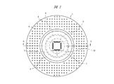
<プローブカードの全体構造>
図1は本実施の形態のプローブカードの下面の要部平面図であり、図2は図1中のA−A線に沿った断面図、図3はそのプローブが形成された領域の要部拡大断面図である。
<Overall structure of probe card>
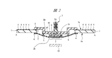
1 is a plan view of the main part of the lower surface of the probe card of the present embodiment, FIG. 2 is a cross-sectional view taken along the line AA in FIG. 1, and FIG. 3 is a main part of the region where the probe is formed. It is an expanded sectional view.
図1および図2に示すように、本実施の形態のプローブカードは、たとえば多層配線基板(第1配線基板)1、薄膜シート(薄膜プローブ、第1シート)2およびプランジャ(押圧機構)3などから形成されている。 As shown in FIGS. 1 and 2, the probe card of the present embodiment includes, for example, a multilayer wiring board (first wiring board) 1, a thin film sheet (thin film probe, first sheet) 2, a plunger (pressing mechanism) 3, and the like. Formed from.
多層配線基板1はその中央に平面円形状の開口部5を有する平面円形枠状のプリント多層配線基板によって形成されている。
The
この多層配線基板1の下面(第2主面)1b中央には上記開口部5を塞ぐように薄膜シート2がその外周を押さえるように設けられた押さえリング(第1固定治具)4によって多層配線基板1の下面(第2主面)1bに固定されている。
At the center of the lower surface (second main surface) 1b of the
薄膜シート2は、例えばポリイミドが主成分の樹脂を絶縁材料とする可撓性(柔軟性)を有する配線基板によって形成されている。この薄膜シート2の下面(第2主面)2bの中央には複数のプローブ(接触端子)7が配置されている。各プローブ7の形状は4角錐型または4角錐台形型となっている。
薄膜シート2内には、プローブ7の各々と電気的に接続し、薄膜シート2の下面2b中央のプローブ7が形成された領域から外周縁に向かって延在する複数の配線(第2配線)が形成されている。多層配線基板1の下面1bには、この複数の配線の端部とそれぞれ電気的に接触する複数の受け部(図示は省略)が形成されており、この複数の受け部は、多層配線基板1内に形成された配線(第1配線)を通じて多層配線基板1の上面(第1主面)1aに設けられた複数のポゴ(POGO)座8と電気的に接続している。このポゴ座8は、テスタからの信号をプローブカードへ導入するピンを受ける機能を有する。
The
In the
一方、多層配線基板1の上面1a中央(薄膜シート2の上面2a側上方)には、プランジャ3が配置されている。このプランジャ3はプランジャ支持部3Bを介して多層配線基板1に固定されている。またプランジャ支持部3Bは開口部5内において接着リング6によって薄膜シート2と接着されている。
On the other hand, a plunger 3 is arranged at the center of the upper surface 1a of the multilayer wiring board 1 (above the
プランジャ3は多層配線基板1の上面(第1主面)1aに、プランジャ支持部3Bを介して取り付けられている。多層配線基板1の中央部には開口部5が設けられ、この開口部5内において、薄膜シート2とプランジャ3とは接着リング6を介して接着されている。
The plunger 3 is attached to the upper surface (first main surface) 1a of the
薄膜シート2の下面(第2主面)2bには、たとえば4角錐型または4角錐台形型の複数のプローブ7が形成されている。
On the lower surface (second main surface) 2 b of the
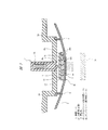
プランジャ3と薄膜シート2の間には押圧具(押圧機構)9が配置されている。押圧具9は例えば平面円形状の金属板であり、その材質としては42アロイのようなポリイミドよりも硬い金属材料を例示することができる。押圧具9の主面(押圧面)9bは略平坦に形成され、上下方向に移動可能になっている。
A pressing tool (pressing mechanism) 9 is disposed between the plunger 3 and the
本実施の形態では、チップ(チップ領域)10のパッドにすべてのプローブ7を接触させるために、プローブ7が形成された領域(第1領域)の薄膜シート2を上面(第1主面)2a側から押圧具(押圧機構)9をプランジャ(押圧機構)3が押圧する構造となっている。すなわち、プランジャ3内に配置されたばね3Aの弾性力によって一定の圧力を押圧具9に加えるものである。
In the present embodiment, in order to bring all the
ここで、図3に示すように押圧具9の主面9bと薄膜シート2の上面2aとの間には、例えばシリコーンなどのエラストマシート(第1中間シート)45と、ポリイミドシート(第2中間シート)46とが配置されている。
Here, as shown in FIG. 3, between the
エラストマシート45と、ポリイミドシート46は、それぞれ厚さ方向に沿って互いに反対側に位置する上面(第1主面)45a、46aと下面(第2主面)45b、46bとを有している。
The
エラストマシート45はその下面(第2主面)45bが、薄膜シート2の上面2aと対向接触した状態で配置されている。エラストマシート45が配置される平面位置は、薄膜シート2の下面2b側に複数のプローブ7が形成された領域に対応する位置となっている。
The
また、エラストマシート45の上面(第1主面)45a側に配置されるポリイミドシート46は、その上面(第1主面)46aが押圧具9の主面9bと対向接触した状態で配置される。ポリイミドシート46が配置される平面位置も、エラストマシート45と同様に薄膜シート2の下面2b側に複数のプローブ7が形成された領域に対応する位置となっている。
The
このポリイミドシート46はエラストマシート45よりも滑りやすい特徴を有している。仮に、エラストマシート45の上面45aと押圧具9の主面9bとを対向接触させた場合、その接触面の摩擦係数は約0.8である。一方、図3に示すポリイミドシート46の上面46aと押圧具9の主面9bとを対向接触させた接触面の摩擦係数は約0.3とエラストマシート45の場合よりも小さい。
The
一方、エラストマシート45はポリイミドシートよりも柔らかく、外力によって変形し易い特徴を有している。
On the other hand, the
本実施の形態のプローブカードは上記構成とすることにより、プローブ検査において、プローブ7とそのプローブ7が対応するチップ10のパッドとを所望の接触圧力範囲内に接触させることができる。この理由については、薄膜シート2の詳細な構造を説明した後で詳述する。
By adopting the above configuration, the probe card of the present embodiment can bring the
<プローブ検査の対象>
本実施の形態において、上記プローブカードを用いてプローブ検査(電気的検査)を行う対象としては、LCD(Liquid Crystal Display)ドライバが形成されたチップを例示することができる。図4は、そのチップ(チップ領域)10の平面と、その一部を拡大したものを図示している。このチップ10は、たとえば単結晶シリコン基板からなり、その主面にはLCDドライバ回路が形成されている。また、チップ10の主面の周辺部には、LCDドライバ回路と電気的に接続する多数のパッド(第1電極)11、12が配置されており、図4中におけるチップ10の上側の長辺および両短辺に沿って配列されたパッド11は出力端子となり、チップ10の下側の長辺に沿って配列されたパッド12は入力端子となっている。LCDドライバの出力端子数は入力端子数より多いことから、隣り合ったパッド11の間隔をできる限り広げるために、パッド11はチップ10の上側の長辺および両短辺に沿って2列で配列され、チップ10の上側の長辺および両短辺に沿って互いの列のパッド11が互い違いに配列されている。本実施の形態において、隣り合うパッド11が配置されているピッチLPは、たとえば約68μmである。また、本実施の形態において、パッド11は平面矩形であり、チップ10の外周と交差(直交)する方向に延在する長辺の長さLAは約63μmであり、チップ10の外周に沿って延在する短辺の長さLBは約34μmである。また、隣り合うパッド11が配置されているピッチLPが約68μmであり、パッド11の短辺の長さLBが約34μmであることから、隣り合うパッド11の間隔は約34μmとなる。
<Target of probe inspection>
In the present embodiment, a chip on which an LCD (Liquid Crystal Display) driver is formed can be exemplified as an object to be subjected to probe inspection (electrical inspection) using the probe card. FIG. 4 illustrates a plane of the chip (chip area) 10 and a part thereof enlarged. The
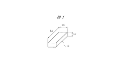
パッド11、12は、たとえばAu(金)から形成されたバンプ電極であり、チップ10の入出力端子(ボンディングパッド)上に、電解めっき、無電解めっき、蒸着あるいはスパッタリングなどの方法によって形成されたものである。図5は、パッド11の斜視図である。パッド11の高さLCは約15μmであり、パッド12も同程度の高さを有する。
The
また、上記チップ10は、ウエハの主面に区画された多数のチップ領域に半導体製造技術を使ってLCDドライバ回路(半導体集積回路)や入出力端子(ボンディングパッド)を形成し、次いで入出力端子上に上記の方法でパッド11を形成した後、ウエハをダイシングしてチップ領域を個片化することにより製造することができる。また、本実施の形態において、上記プローブ検査は、ウエハをダイシングする前に各チップ領域に対して実施するものである。なお、以後プローブ検査(パッド11、12とプローブ7とが接触する工程)を説明する際に、特に明記しない場合には、チップ10はウエハをダイシングする前の各チップ領域を示すものとする。
Further, the
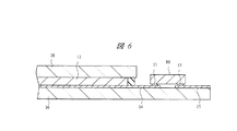
図6は、上記チップ10(ダイシングされた後のもの)の液晶パネルへの接続方法を示す要部断面図である。図6に示すように、液晶パネルは、たとえば主面に画素電極14、15が形成されたガラス基板16、液晶層17、および液晶層17を介してガラス基板16と対向するように配置されたガラス基板18などから形成されている。本実施の形態においては、このような液晶パネルのガラス基板16の画素電極14、15に、それぞれパッド11、12が接続するようにチップ10(ダイシングされた後のもの)をフェイスダウンボンディングすることによって、チップ10を液晶パネルへ接続することを例示できる。
FIG. 6 is a cross-sectional view of the main part showing a method for connecting the chip 10 (after being diced) to the liquid crystal panel. As shown in FIG. 6, the liquid crystal panel is disposed so as to face the glass substrate 16 with the glass substrate 16 having the
<プローブの配置>
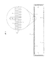
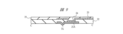
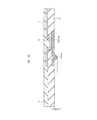
図7は上記薄膜シート2の下面の複数のプローブ7が形成された領域の一部を拡大して示した要部平面図であり、図8は図7中のB−B線に沿った要部断面図であり、図9は図7中のC−C線に沿った要部断面図、図10は本実施の形態1のプローブカードを形成する薄膜シートの要部を拡大して示す断面図である。
<Probe placement>
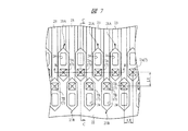
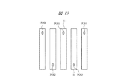
FIG. 7 is an enlarged plan view of a main part of a part of the lower surface of the
上記プローブ7は、薄膜シート2中にて平面六角形状にパターニングされた金属膜21A、21Bの一部であり、金属膜21A、21Bのうちの薄膜シート2の下面に4角錐型または4角錐台形型に飛び出した部分である。プローブ7は、薄膜シート2の下面2bにおいて上記チップ10(図4参照)に形成されたパッド11、12(図4参照)の位置に合わせて配置されており、図7ではパッド11に対応するプローブ7A、7Bの配置について示している。これらプローブ7のうち、プローブ7Aは、2列で配列されたパッド11のうちの相対的にチップ10の外周に近い配列(以降、第1列と記す)のパッド11に対応し、プローブ7Bは、2列で配列されたパッド11のうちの相対的にチップ10の外周から遠い配列(以降、第2列と記す)のパッド11に対応している。また、最も近い位置に存在するプローブ7Aとプローブ7Bとの間の距離は、図7が記載された紙面の左右方向の距離LXと上下方向の距離LYとで規定され、距離LXは前述の隣り合うパッド11が配置されているピッチLPの半分の約34μmとなる。また、本実施の形態において、距離LYは、約93μmとなる。また、図10に示すように、ポリイミド膜22の表面からプローブ7A、7Bの先端までの高さLZ(針高さ)は、50μm以下(大きくとも90μm以下)、更に望ましくは30μm以下で揃えられている。
The
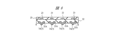
金属膜21A、21Bは、たとえば下層からロジウム膜およびニッケル膜が順次積層されて形成されている。金属膜21A、21B上にはポリイミド膜22が成膜され、ポリイミド膜22上には各金属膜21A、21Bと電気的に接続する配線(第2配線)23が形成されている。配線23は、ポリイミド膜22に形成されたスルーホール24の底部で金属膜21A、21Bと接触している。また、ポリイミド膜22および配線23上には、ポリイミド膜25が成膜されている。
The
上記したように、金属膜21A、21Bの一部は4角錐型または4角錐台形型に形成されたプローブ7A、7Bとなり、ポリイミド膜22には金属膜21A、21Bに達するスルーホール24が形成される。そのため、プローブ7Aが形成された金属膜21Aおよびスルーホール24の平面パターンと、プローブ7Bが形成された金属膜21Bおよびスルーホール24の平面パターンとが同じ方向で配置されるようにすると、隣り合う金属膜21Aと金属膜21Bとが接触してしまい、プローブ7A、7Bからそれぞれ独立した入出力を得られなくなってしまう不具合が懸念される。そこで、本実施の形態では、図7に示すように、プローブ7Bが形成された金属膜21Bおよびスルーホール24の平面パターンは、プローブ7Aが形成された金属膜21Aおよびスルーホール24の平面パターンを180°回転したパターンとしている。それにより、平面でプローブ7Aおよびスルーホール24が配置された金属膜21Aの幅広の領域と、平面でプローブ7Bおよびスルーホール24が配置された金属膜21Bの幅広の領域とが、紙面の左右方向の直線上に配置されないようになり、金属膜21Aおよび金属膜21Bの平面順テーパー状の領域が紙面の左右方向の直線上に配置されるようになる。その結果、隣り合う金属膜21Aと金属膜21Bとが接触してしまう不具合を防ぐことができる。また、狭ピッチでパッド11(図4参照)が配置されても、それに対応した位置にプローブ7A、7Bを配置することが可能となる。
As described above, a part of the
本実施の形態では、図4を用いてパッド11が2列で配列されている場合について説明したが、図11に示すように、1列で配列されているチップも存在する。そのようなチップに対しては、図12に示すように、上記金属膜21Aの幅広の領域が紙面の左右方向の直線上に配置された薄膜シート2を用いることで対応することができる。また、このようにパッド11が1列で配列され、たとえばチップ10の外周と交差(直交)する方向に延在する長辺の長さLA約140μmであり、チップ10の外周に沿って延在する短辺の長さLBが約19μmであり、隣り合うパッド11が配置されているピッチLPが約34μmであり、隣り合うパッド11の間隔が約15μmである場合には、図4に示したパッド11に比べて長辺が約2倍以上となり、短辺方向でのパッド11の中心位置を図4に示したパッド11の中心位置と揃えることができるので、図7〜図9を用いて説明した薄膜シート2を用いることが可能となり、図13に示す位置POS1、POS2でプローブ7A、7Bのそれぞれがパッド11に接触することになる。
In this embodiment, the case where the
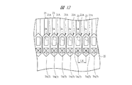
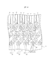
また、パッド11の数がさらに多い場合には、3列以上で配列されている場合もある。図14は3列で配列されたパッド11に対応した薄膜シート2の要部平面図であり、図15は4列で配列されたパッド11に対応した薄膜シート2の要部平面図である。チップ10のサイズが同じであれば、パッド11の配列数が増えるに従って、図7を用いて説明した距離LXがさらに狭くなるので、上記金属膜21A、21Bを含む金属膜が接触してしまうことがさらに懸念される。そこで、図14および図15に示すように、金属膜21A、21B、21C、21Dを、たとえば図7に示した金属膜21Aの平面パターンを45°回転させたものとすることで、金属膜21A、21B、21C、21Dが互いに接触してしまう不具合を防ぐことが可能となる。また、ここでは図7に示した金属膜21Aの平面パターンを45°回転させた例について説明したが、45°に限定するものではなく、金属膜21A、21B、21C、21Dの互いの接触を防ぐことができるのであれば他の回転角でもよい。なお、金属膜21Cには、プローブ7Bが対応するパッド11よりさらにチップ10内の内側に配置されたパッド11に対応するプローブ7Cが形成され、金属膜21Dには、プローブ7Cが対応するパッド11よりさらにチップ10内の内側に配置されたパッド11に対応するプローブ7Dが形成されている。
In addition, when the number of
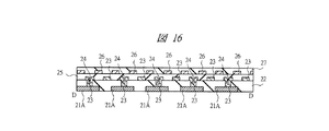
ここで、図16は図15中のD−D線に沿った要部断面図であり、図17は図15中のE−E線に沿った要部断面図である。図15に示したように、4列のパッド11に対応するプローブ7A〜7Dを有する金属膜21A〜21Dを配置した場合には、金属膜21A〜21Dのそれぞれに上層から電気的に接続する配線のすべてを同一の配線層で形成することが困難になる。これは、上記距離LXが狭くなることによって、金属膜21A〜21Dのそれぞれ同士が接触する虞が生じるのと共に、金属膜21A〜21Dに電気的に接続する配線同士も接触する虞が生じるからである。そこで、本実施の形態においては、図16および図17に示すように、それら配線を2層の配線層(配線23、26)から形成することを例示することができる。なお、配線26およびポリイミド膜25上には、ポリイミド膜27が形成されている。相対的に下層の配線23はポリイミド膜22に形成されたスルーホール24の底部で金属膜21A、21Cと接触し、相対的に上層の配線26はポリイミド膜22、25に形成されたスルーホール28の底部で金属膜21B、21Dと接触している。それにより、同一の配線層においては、隣り合う配線23または配線26の間隔を大きく確保することが可能となるので、隣り合う配線23または配線26が接触してしまう不具合を防ぐことができる。また、パッド11が5列以上となり、それに対応するプローブ数が増加して上記距離LXが狭くなる場合には、さらに多層に配線層を形成することによって、配線間隔を広げてもよい。
Here, FIG. 16 is a cross-sectional view of main parts along the line DD in FIG. 15, and FIG. 17 is a cross-sectional view of main parts along the line EE in FIG. As shown in FIG. 15, when the
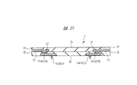
<薄膜シートの詳細構造および製造方法>
次に、上記の本実施の形態の薄膜シート2の構造について、その製造工程と併せて図18〜図23を用いて説明する。図18〜図23は、図7〜図9を用いて説明した2列のパッド11(図4参照)に対応したプローブ7A、7Bを有する薄膜シート2の製造工程中の要部断面図である。
<Detailed structure and manufacturing method of thin film sheet>
Next, the structure of the
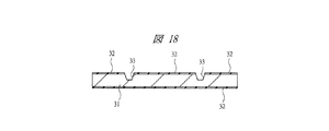
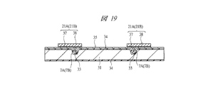
まず、図18に示すように、厚さ0.2mm〜0.6mm程度のシリコンからなるウエハ31を用意し、熱酸化法によってこのウエハ31の両面に膜厚0.5μm程度の酸化シリコン膜32を形成する。続いて、フォトレジスト膜をマスクとしてウエハ31の主面側の酸化シリコン膜32をエッチングし、ウエハ31の主面側の酸化シリコン膜32にウエハ31に達する開口部を形成する。次いで、残った酸化シリコン膜32をマスクとし、強アルカリ水溶液(たとえば水酸化カリウム水溶液)をもちいてウエハ31を異方的にエッチングすることによって、ウエハ31の主面に(111)面に囲まれた4角錐型または4角錐台形型の穴33を形成する。
First, as shown in FIG. 18, a
次に、図19に示すように、上記穴33の形成時にマスクとして用いた酸化シリコン膜32をフッ酸およびフッ化アンモニウムの混合液によるウェットエッチングにより除去する。続いて、ウエハ31に熱酸化処理を施すことにより、穴33の内部を含むウエハ31の全面に膜厚0.5μm程度の酸化シリコン膜34を形成する。次いで、穴33の内部を含むウエハ31の主面に導電性膜35を成膜する。この導電性膜35は、たとえば膜厚0.1μm程度のクロム膜および膜厚1μm程度の銅膜を順次スパッタリング法または蒸着法によって堆積することによって成膜することができる。次いで、導電性膜35上にフォトレジスト膜を成膜し、フォトリソグラフィ技術によって後の工程で金属膜21A、21B(図7〜図9参照)が形成される領域のフォトレジスト膜を除去し、開口部を形成する。
Next, as shown in FIG. 19, the
次に、導電性膜35を電極とした電解めっき法により、上記フォトレジスト膜の開口部の底部に現れた導電性膜35上に硬度の高い導電性膜37および導電性膜38を順次堆積する。本実施の形態においては、導電性膜37をロジウム膜とし、導電性膜38をニッケル膜とすることを例示できる。ここまでの工程により、導電性膜37、38から前述の金属膜21A、21Bを形成することができる。また、穴33内の導電性膜37、38が前述のプローブ7A、7Bとなる。なお、導電性膜35は、後の工程で除去されるが、その工程については後述する。
Next, a
金属膜21A、21Bにおいては、後の工程で前述のプローブ7A、7Bが形成された時に、ロジウム膜から形成された導電性膜37が表面となり、導電性膜37がパッド11に直接接触することになる。そのため、導電性膜37としては、硬度が高く耐磨耗性に優れた材質を選択することが好ましい。また、導電性膜37はパッド11に直接接触するため、プローブ7A、7Bによって削り取られたパッド11の屑が導電性膜37に付着すると、その屑を除去するクリーニング工程が必要となり、プローブ検査工程が延びてしまうことが懸念される。そのため、導電性膜37としては、パッド11を形成する材料が付着し難い材質を選択することが好ましい。そこで、本実施の形態においては、導電性膜37として、これらの条件を満たすロジウム膜を選択している。それにより、そのクリーニング工程を省略することができる。
In the metal films 21 </ b> A and 21 </ b> B, when the above-described
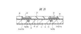
次に、上記金属膜21A、21B(導電性膜37、38)の成膜に用いたフォトレジスト膜を除去した後、図20に示すように、金属膜21A、21Bおよび導電性膜35を覆うようにポリイミド膜22(図8および図9も参照)を成膜する。続いて、そのポリイミド膜22に金属膜21A、21Bに達する前述のスルーホール24を形成する。このスルーホール24は、レーザを用いた穴あけ加工またはアルミニウム膜をマスクとしたドライエッチングによって形成することができる。
Next, after removing the photoresist film used to form the
次に、図21に示すように、スルーホール24の内部を含むポリイミド膜22上に導電性膜42を成膜する。この導電性膜42は、たとえば膜厚0.1μm程度のクロム膜および膜厚1μm程度の銅膜を順次スパッタリング法または蒸着法によって堆積することによって成膜することができる。続いて、その導電性膜42上にフォトレジスト膜を形成した後に、そのフォトレジスト膜をフォトリソグラフィ技術によってパターニングし、フォトレジスト膜に導電性膜42に達する開口部を形成する。次いで、めっき法により、その開口部内の導電性膜42上に導電性膜43を成膜する。本実施の形態においては、導電性膜43として銅膜、または銅膜およびニッケル膜を下層から順次堆積した積層膜を例示することができる。
Next, as shown in FIG. 21, a
次に、上記フォトレジスト膜を除去した後、導電性膜43をマスクとして導電性膜42をエッチングすることにより、導電性膜42、43からなる配線23を形成する。配線23は、スルーホール24の底部にて金属膜21A、21Bと電気的に接続することができる。
Next, after removing the photoresist film, the
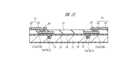
次に、図22に示すように、ウエハ31の主面に前述のポリイミド膜25を成膜する。この工程では、例えば、ポリイミド膜22および配線23の表面にペースト状のポリイミドの前駆体を塗布した後、これをイミド化させて成膜することができる。
Next, as shown in FIG. 22, the
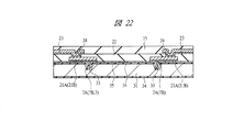
次に、図23に示すように、たとえばフッ酸とフッ化アンモニウムの混合液を用いたエッチングによって、ウエハ31の裏面の酸化シリコン膜34を除去する。続いて、強アルカリ水溶液(たとえば水酸化カリウム水溶液)を用いたエッチングにより、薄膜シート2を形成するための型材であるウエハ31を除去する。次いで、酸化シリコン膜34および導電性膜35を順次エッチングにより除去する。この時、酸化シリコン膜34はフッ酸およびフッ化アンモニウムの混合液を用いてエッチングし、導電性膜35に含まれるクロム膜は過マンガン酸カリウム水溶液を用いてエッチングし、導電性膜35に含まれる銅膜はアルカリ性銅エッチング液を用いてエッチングする。ここまでの工程により、プローブ7A、7Bを形成する導電性膜37(図19参照)であるロジウム膜がプローブ7A、7Bの表面に現れ、薄膜シート2が得られる。前述したように、ロジウム膜が表面に形成されたプローブ7A、7Bにおいては、プローブ7A、7Bが接触するパッド11の材料であるAuなどが付着し難く、Niより硬度が高く、かつ酸化され難く接触抵抗を安定させることができる。
Next, as shown in FIG. 23, the
<プローブ検査>
次に、本実施の形態のプローブカードを用いてプローブ検査を行う際のエラストマシートと薄膜シートの接触面の状態について本実施の形態の比較例と対比しながら説明する。
<Probe inspection>
Next, the state of the contact surface between the elastomer sheet and the thin film sheet when performing probe inspection using the probe card of the present embodiment will be described in comparison with a comparative example of the present embodiment.
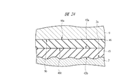
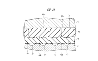
図24は、本実施の形態のプローブカードを用いてプローブ検査を行う際のエラストマシートと薄膜シートの接触面の拡大断面図、図25は本実施の形態の比較例であるプローブカードを用いてプローブ検査を行う際のエラストマシートと薄膜シートの接触面の拡大断面図である。 FIG. 24 is an enlarged sectional view of a contact surface between an elastomer sheet and a thin film sheet when performing a probe inspection using the probe card of the present embodiment, and FIG. 25 is a probe card which is a comparative example of the present embodiment. It is an expanded sectional view of the contact surface of an elastomer sheet and a thin film sheet when performing probe inspection.
図24において、本実施の形態のプローブカードは、薄膜シート2の上面2a上にエラストマシート45、ポリイミドシート46が順に配置されている。一方、図25に示す本実施の形態の比較例であるプローブカードの薄膜シート2の上面2a上には、ポリイミドシート46、エラストマシート45の順で配置されている。
24, in the probe card of the present embodiment, an
ここで、薄膜シート2の上面2aの表面は図24および図25に示すようにミクロンオーダの微細な凹凸を有している。このような凹凸は、例えば、図22で説明したポリイミド膜25を形成する際に、配線23を覆う部分が配線23に倣って盛り上がることにより形成される。また例えば、完成した薄膜シート2を組み立てる際に、微細な皺が発生してこれが薄膜シート2の上面2a表面の凹凸となる場合もある。
Here, the surface of the
図25に示すように、表面に凹凸を有する薄膜シート2の上面2aにポリイミドシート46を対向接触させる場合、ポリイミドシート46の剛性が高いため、その接触面に隙間47が発生する。
As shown in FIG. 25, when the
この状態で押圧具9により押圧すると、ポリイミドシート46と薄膜シート2とが接触している領域には強い荷重が伝達され、隙間47が発生した領域には弱い荷重が伝達される。つまり、面圧分布(平面上の荷重の分布)がばらつく結果となる。
When the
このため、図2に示す薄膜シート2の下面2bに形成された複数のプローブ7とチップ10の主面に形成された複数のパッド11、12(図4参照)との接触圧力にばらつきが生じる。
For this reason, variation occurs in contact pressure between the plurality of
そこで、本実施の形態では、図24に示すように表面に凹凸を有する薄膜シート2の上面2aにエラストマシート45を対向接触させる構成とした。エラストマシート45はポリイミドシート46と比較して柔らかく、変形し易い。このため、押圧具9により押圧すると、図24に示すように薄膜シート2の上面2aの凹凸に沿って変形する。つまり、図25に示すような隙間47の発生を抑制することができる。
Therefore, in the present embodiment, as shown in FIG. 24, the
したがって、押圧具9から伝えられた荷重をより均等に近い形で分布させることができるので、図2に示す薄膜シート2の下面2bに形成されたプローブ7とチップ10の主面に形成されたパッド11、12(図4参照)との接触圧力を所定の範囲内に収めることができる。
Therefore, since the load transmitted from the
つまり、プローブ7から過荷重が加わることによるチップ10の破損や、プローブ7の磨耗を防止ないしは抑制することが出来る。また、プローブ7の接触圧力が過小荷重となることによる接触不良を防止することができる。
That is, it is possible to prevent or suppress damage to the
また、プローブ検査を行う際の雰囲気温度が高温、あるいは低温に設定された場合には、薄膜シート2、ポリイミドシート46、エラストマシート45、押圧具9はそれぞれ熱膨張、あるいは収縮する。
Further, when the ambient temperature during probe inspection is set to a high temperature or a low temperature, the
特に、押圧具9は42アロイなどの金属材料で構成されるため、その線膨張係数はポリイミドシート46、エラストマシート45などの樹脂材料の線膨張係数よりも非常に高い。すなわち、押圧具9はポリイミドシート46、エラストマシート45よりも熱膨張、あるいは熱収縮し易い。
In particular, since the
ここで、図25に示すように押圧具9の主面9bと対向接触する中間シートがエラストマシート45である場合、その接触面の摩擦係数が約0.8と高い。このため、エラストマシート45は熱変形した押圧具9に引っ張られて変形する。この変形の方向は押圧具9とエラストマシート45の接触面に沿った方向に変形し易い。一方、このエラストマシート45は線膨張係数が大きく変形の程度が大きい。この場合、エラストマシート45の下面(第2主面)45bと対向接触するポリイミドシート46の上面46aとの摩擦係数も約0.8程度と高いため、押圧具9の熱変形の影響を含めたエラストマシート45の熱変形がポリイミドシート46に伝わり、ポリイミドシート46に例えば皺が発生するなどの影響を与える場合がある。
Here, when the intermediate sheet facing the
ポリイミドシート46に皺が発生した場合、ポリイミドシート46と薄膜シート2の上面2aとの間の隙間47は大きくなるので、前述したように、押圧具9から伝達される面圧分布(平面上の荷重の分布)がばらつく。この結果、図2に示す薄膜シート2の下面2bに形成された複数のプローブ7とチップ10の主面に形成された複数のパッド11、12(図4参照)との接触圧力にばらつきが生じる。
When wrinkles occur in the
そこで、本実施の形態では図24に示すように押圧具9とポリイミドシート46とを対向接触させる構成とした。押圧具9とポリイミドシート46との接触面ではその摩擦係数が約0.3と低いので滑りやすい。したがって、押圧具9が熱変形した場合に、ポリイミドシート46との接触面が引っ張られることを防止ないしは抑制することができる。このため、押圧具9が膨張、あるいは収縮してもポリイミドシート46はその影響を受けにくい。
Therefore, in this embodiment, as shown in FIG. 24, the
一方、ポリイミドシート46とエラストマシート45との接触面では、その摩擦係数が約0.8と高い。しかし、エラストマシート45の上下面と接触している材質は線膨張係数が近い材質で有るためにエラストマシート45の表面の伸び量は殆ど同じ大きさであるとともに、エラストマシート45は柔らかく、変形し易いので、ポリイミドシート46の変形に対応して平面的に変形する。このためポリイミドシート46とエラストマシート45との線膨張係数が異なっていてもポリイミドシート46あるいはエラストマシート45の皺の発生を抑制することができる。また、ポリイミドシート46とエラストマシート45は密着状態を維持することができる。
On the other hand, the friction coefficient of the contact surface between the
したがって、図2に示す薄膜シート2の下面2bに形成されたプローブ7の配置ピッチは、薄膜シート2自身の熱膨張、あるいは収縮のみを考慮すれば良く、押圧具9、ポリイミドシート46、エラストマシート45の影響を考慮しなくても良いので容易な設計が可能となる。
Therefore, the arrangement pitch of the
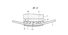
<プローブカードの組み立て>
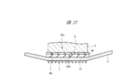
次に、本実施の形態のプローブカードの組み立てについて説明する。図26および図27は本実施の形態のプローブカードの組み立て工程を示す要部断面図である。
<Assembly of probe card>
Next, assembly of the probe card according to the present embodiment will be described. 26 and 27 are cross-sectional views of the main part showing the assembly process of the probe card of the present embodiment.
まず、図26に示すように薄膜シート2を準備して、その上面2a側にエラストマシート45、ポリイミドシート46を順次配置して積層する。エラストマシート45およびポリイミドシート46を配置する平面位置は、薄膜シート2の下面2b側にプローブ7が形成された領域に対応した位置に配置する。
First, as shown in FIG. 26, the
エラストマシート45およびポリイミドシート46を配置する工程では、各シートの密着性を確保するため、薄膜シート2が平面の状態(撓んでいない状態)で配置することが好ましい。
In the step of disposing the
次に、薄膜シート2の一部(例えば外縁部)を図2に示す押さえリング4によって多層配線基板1の下面1bに固定する。この時、薄膜シート2、エラストマシート45、ポリイミドシート46は柔軟性を有しているため、図26に示すように各シートは撓んだ状態となる。
Next, a part (for example, outer edge portion) of the
次に、図27に示すように押圧具9を下方向(薄膜シート2に向かう方向)に押し下げて、薄膜シート2、エラストマシート45、ポリイミドシート46、押圧具9をそれぞれ密着させる。
Next, as shown in FIG. 27, the
ここで、押圧具9とエラストマシート45との間にポリイミドシート46を有さない構成とした場合、押圧具9の主面9bの外縁部が撓んだ状態のエラストマシート45と最初に接触する。しかし、エラストマシート45と押圧具9との摩擦係数が高いため、エラストマシート45の押圧具9の主面9bの外縁部と接触した領域は押圧具9に拘束され、撓んだ状態を矯正することができない。このためエラストマシート45と押圧具9の間に大きな空間が形成される。あるいはエラストマシート45に大きな皺が発生する。
Here, when it is set as the structure which does not have the
一方、本実施の形態では、押圧具9の主面9bと、ポリイミドシート46の上面46aとが対向接触する。ポリイミドシート46の上面46aと押圧具9の主面9bとを対向接触させた接触面の摩擦係数は0.3と小さい。したがって、ポリイミドシート46と押圧具9の接触面では滑りが発生する。このため、ポリイミドシート46の押圧具9の主面9bの外縁部と接触した領域は押圧具9に拘束されず、ポリイミドシート46の撓んだ状態を矯正することができる。
On the other hand, in the present embodiment, the
また、エラストマシート45の下面45bと薄膜シート2の上面2aの接触面は既に密着した状態なので図27に示すように薄膜シート2およびエラストマシート45は押圧具9の主面9bに沿って平面化される。つまり、図26に示す各シート(薄膜シート2、エラストマシート45、ポリイミドシート46)の撓みを矯正することができる。
Since the contact surface between the
本実施の形態では、薄膜シート2の上面2a側にエラストマシート45、ポリイミドシート46を順次配置して積層することにより、薄膜シート2の上面2aとエラストマシート45の下面45bとが対向接触した構成としても、皺や撓みの発生を抑制することができる。このため、図2に示す薄膜シート2の下面2bに形成されたプローブ7とチップ10の主面に形成されたパッド11、12(図4参照)との接触圧力を所定の範囲内に収めることができる。
In the present embodiment, an
また、図27に示すように、ポリイミドシート46の上面46aの平面積は押圧具9の主面9bの平面積よりも大きくすることが好ましい。図27に示すように押圧具9を下方向に押し下げた時にポリイミドシート46と押圧具9との接触面で滑りが発生しても、押圧具9の主面9b全体をポリイミドシート46で覆うことが出来るからである。
In addition, as shown in FIG. 27, the plane area of the
以上、本発明者によってなされた発明を実施の形態に基づき具体的に説明したが、本発明は上記実施の形態に限定されるものではなく、その要旨を逸脱しない範囲で種々変更可能であることは言うまでもない。 As mentioned above, the invention made by the present inventor has been specifically described based on the embodiment. However, the present invention is not limited to the above embodiment, and various modifications can be made without departing from the scope of the invention. Needless to say.
例えば、本実施の形態ではエラストマシート45の上面45a上に1枚のポリイミドシート46を配置した例について説明したが、ポリイミドシート46の枚数はこれに限定されない。例えば、エラストマシート45の上面45a上に2枚以上のポリイミドシート46を積層して配置しても良い。
For example, in the present embodiment, an example in which one
この場合であっても、最上層のポリイミドシート46の上面46aと押圧具9の主面9bとが対向接触していれば、接触面の摩擦抵抗を抑制することができるので、ポリイミドシート46あるいはエラストマシート45における皺の発生を抑制することができる。
Even in this case, if the
また、組み立て工程においては、薄膜シート2の上面2aにエラストマシート45を配置した後、複数枚のポリイミドシート46を順次積層することにより、各シート(薄膜シート2、エラストマシート45、ポリイミドシート46)の撓みを矯正することができる。
In the assembly process, after placing the
本発明の半導体装置の製造方法は、たとえば半導体装置の製造工程におけるプローブ検査工程に広く適用することができる。 The semiconductor device manufacturing method of the present invention can be widely applied to, for example, a probe inspection process in a semiconductor device manufacturing process.
1 多層配線基板(第1配線基板)
1a 上面(第1主面)
1b 下面(第2主面)
2 薄膜シート(薄膜プローブ、第1シート)
2a 上面(第1主面)
2b 下面(第2主面)
3 プランジャ
3A ばね
3B プランジャ支持部
4 押さえリング(第1固定治具)
5 開口部
6 接着リング
7、7A、7B、7C、7D プローブ(接触端子)
8 ポゴ座
9 押圧具(押圧機構)
9b 主面
10 チップ(チップ領域)
11、12 パッド(第1電極)
14、15 画素電極
16、18 ガラス基板
17 液晶層
21A、21B、21C、21D 金属膜
22 ポリイミド膜
23 配線
24 スルーホール
25 ポリイミド膜
26 配線
27 ポリイミド膜
28 スルーホール
31 ウエハ
32 酸化シリコン膜
33 穴
34 酸化シリコン膜
35、37、38 導電性膜
42、43 導電性膜
45 エラストマシート(第1中間シート)
45a 上面(第1主面)
45b 下面(第2主面)
46 ポリイミドシート(第2中間シート)
46a 上面(第1主面)
46b 下面(第2主面)
47 隙間
1 Multilayer wiring board (first wiring board)
1a Upper surface (first main surface)
1b Lower surface (second main surface)
2 Thin film sheet (thin film probe, first sheet)
2a Upper surface (first main surface)
2b Lower surface (second main surface)
3
5
8
11, 12 Pad (first electrode)
14, 15
45a Upper surface (first main surface)
45b Lower surface (second main surface)
46 Polyimide sheet (second intermediate sheet)
46a Upper surface (first main surface)
46b Lower surface (second main surface)
47 Clearance
Claims (3)
(b)前記半導体ウエハの前記チップ領域に形成された前記複数の第1電極に、プローブカードの第1シートの第2主面に形成された複数の接触端子をそれぞれ接触させた状態で、前記チップ領域に形成された前記素子の電気的検査を行う工程とを含み、
前記プローブカードは、
前記第1シートと、
前記第1シートの前記第2主面の裏側の第1主面側に配置され、前記(b)工程において、前記第1シートの前記第1主面側を押圧し、前記複数の接触端子を前記半導体ウエハの前記チップ領域の前記複数の第1電極に押し当てる押圧具を有する押圧機構と、
前記第1シートと前記押圧具との間に配置された中間シートとを有し、
前記中間シートは、
前記第1シートの前記第1主面側に対向接触して配置される第1中間シートと、
前記押圧具に対向接触して配置される第2中間シートとを有し、
前記第1中間シートは、エラストマにより形成されており、
前記第2中間シートと前記押圧具とを接触させた場合の摩擦係数は、前記第1中間シートと前記押圧具とを接触させた場合の摩擦係数よりも小さいことを特徴とする半導体装置の製造方法。 (A) A semiconductor wafer partitioned into a plurality of chip regions, each having a device formed in each of the plurality of chip regions, and a plurality of first electrodes electrically connected to the device formed on a main surface thereof. The process to prepare,
(B) With the plurality of contact terminals formed on the second main surface of the first sheet of the probe card in contact with the plurality of first electrodes formed in the chip region of the semiconductor wafer, Performing an electrical inspection of the element formed in the chip region,
The probe card is
The first sheet;
The first sheet is disposed on the first main surface side behind the second main surface of the first sheet, and in the step (b), the first main surface side of the first sheet is pressed, and the plurality of contact terminals are arranged. A pressing mechanism having a pressing tool that presses against the plurality of first electrodes in the chip region of the semiconductor wafer;
An intermediate sheet disposed between the first sheet and the pressing tool;
The intermediate sheet is
A first intermediate sheet disposed to face and face the first main surface of the first sheet;
A second intermediate sheet that is disposed opposite to the pressing tool,
The first intermediate sheet is formed of an elastomer,
A semiconductor device manufacturing method, wherein a friction coefficient when the second intermediate sheet and the pressing tool are brought into contact is smaller than a friction coefficient when the first intermediate sheet and the pressing tool are brought into contact with each other. Method.
前記第2中間シートはポリイミドにより形成されることを特徴とする半導体装置の製造方法。 In the manufacturing method of the semiconductor device according to claim 1,
The method for manufacturing a semiconductor device, wherein the second intermediate sheet is formed of polyimide.
前記中間シートは、前記第1シートの前記第1主面側から、前記第1中間シート、前記第2中間シートを順次積層して配置することを特徴とする半導体装置の製造方法。 In the manufacturing method of the semiconductor device according to claim 1,
The method for manufacturing a semiconductor device, wherein the intermediate sheet is arranged by sequentially laminating the first intermediate sheet and the second intermediate sheet from the first main surface side of the first sheet.
Priority Applications (1)
| Application Number | Priority Date | Filing Date | Title |
|---|---|---|---|
| JP2007294035A JP2009123797A (en) | 2007-11-13 | 2007-11-13 | Manufacturing method of semiconductor device |
Applications Claiming Priority (1)
| Application Number | Priority Date | Filing Date | Title |
|---|---|---|---|
| JP2007294035A JP2009123797A (en) | 2007-11-13 | 2007-11-13 | Manufacturing method of semiconductor device |
Publications (1)
| Publication Number | Publication Date |
|---|---|
| JP2009123797A true JP2009123797A (en) | 2009-06-04 |
Family
ID=40815659
Family Applications (1)
| Application Number | Title | Priority Date | Filing Date |
|---|---|---|---|
| JP2007294035A Pending JP2009123797A (en) | 2007-11-13 | 2007-11-13 | Manufacturing method of semiconductor device |
Country Status (1)
| Country | Link |
|---|---|
| JP (1) | JP2009123797A (en) |
Cited By (1)
| Publication number | Priority date | Publication date | Assignee | Title |
|---|---|---|---|---|
| JP7475436B2 (en) | 2019-09-12 | 2024-04-26 | インターナショナル・ビジネス・マシーンズ・コーポレーション | Compliant Organic Substrate Assembly for Rigid Probes |
-
2007
- 2007-11-13 JP JP2007294035A patent/JP2009123797A/en active Pending
Cited By (1)
| Publication number | Priority date | Publication date | Assignee | Title |
|---|---|---|---|---|
| JP7475436B2 (en) | 2019-09-12 | 2024-04-26 | インターナショナル・ビジネス・マシーンズ・コーポレーション | Compliant Organic Substrate Assembly for Rigid Probes |
Similar Documents
| Publication | Publication Date | Title |
|---|---|---|
| JP4521611B2 (en) | Manufacturing method of semiconductor integrated circuit device | |
| JP4829879B2 (en) | Manufacturing method of semiconductor integrated circuit device | |
| JP5065674B2 (en) | Manufacturing method of semiconductor integrated circuit device | |
| JP2008205042A (en) | Manufacturing method of semiconductor integrated circuit device | |
| JP4825457B2 (en) | Manufacturing method of semiconductor integrated circuit device | |
| KR100980369B1 (en) | Probe Needle Structure and Manufacturing Method of The Same | |
| JP4800007B2 (en) | Manufacturing method of semiconductor integrated circuit device and probe card | |
| JP2007218890A (en) | Probe assembly | |
| JP4372785B2 (en) | Manufacturing method of semiconductor integrated circuit device | |
| TWI385741B (en) | Manufacturing method of semiconductor integrated circuit device | |
| JP5191646B2 (en) | Manufacturing method of semiconductor integrated circuit device | |
| WO1999048147A1 (en) | Process for manufacturing semiconductor device | |
| JP4919365B2 (en) | Manufacturing method of semiconductor integrated circuit | |
| JP2007212472A (en) | Manufacturing method of semiconductor integrated circuit, and probe card | |
| JP2008008774A (en) | Method of manufacturing semiconductor integrated circuit device | |
| JP4940360B2 (en) | Probe card and inspection device | |
| JP4769474B2 (en) | Manufacturing method of semiconductor integrated circuit device | |
| JP4729348B2 (en) | Manufacturing method of semiconductor integrated circuit device | |
| JP2009123797A (en) | Manufacturing method of semiconductor device | |
| JP2008002984A (en) | Method of manufacturing semiconductor integrated circuit device, and probe card | |
| JP2009250697A (en) | Method for manufacturing semiconductor integrated circuit device and membrane type probe card | |
| JP2007121152A (en) | Method of manufacturing semiconductor integrated circuit device, and method of manufacturing probe card | |
| JP4716454B2 (en) | Manufacturing method of semiconductor integrated circuit device | |
| JP2001289875A (en) | Contact probe | |
| JP2007057464A (en) | Probe card, its manufacturing method, and inspection method |
Legal Events
| Date | Code | Title | Description |
|---|---|---|---|
| A711 | Notification of change in applicant |
Free format text: JAPANESE INTERMEDIATE CODE: A712 Effective date: 20100528 |