JP2009108339A - Semiconductor device and its fabrication process - Google Patents
Semiconductor device and its fabrication process Download PDFInfo
- Publication number
- JP2009108339A JP2009108339A JP2007278437A JP2007278437A JP2009108339A JP 2009108339 A JP2009108339 A JP 2009108339A JP 2007278437 A JP2007278437 A JP 2007278437A JP 2007278437 A JP2007278437 A JP 2007278437A JP 2009108339 A JP2009108339 A JP 2009108339A
- Authority
- JP
- Japan
- Prior art keywords
- plating film
- plane
- lead
- semiconductor device
- tin
- Prior art date
- Legal status (The legal status is an assumption and is not a legal conclusion. Google has not performed a legal analysis and makes no representation as to the accuracy of the status listed.)
- Pending
Links
- XDTMQSROBMDMFD-UHFFFAOYSA-N C1CCCCC1 Chemical compound C1CCCCC1 XDTMQSROBMDMFD-UHFFFAOYSA-N 0.000 description 1
- GDOPTJXRTPNYNR-UHFFFAOYSA-N CC1CCCC1 Chemical compound CC1CCCC1 GDOPTJXRTPNYNR-UHFFFAOYSA-N 0.000 description 1
Images


Classifications
-
- H—ELECTRICITY
- H01—ELECTRIC ELEMENTS
- H01L—SEMICONDUCTOR DEVICES NOT COVERED BY CLASS H10
- H01L23/00—Details of semiconductor or other solid state devices
- H01L23/48—Arrangements for conducting electric current to or from the solid state body in operation, e.g. leads, terminal arrangements ; Selection of materials therefor
- H01L23/488—Arrangements for conducting electric current to or from the solid state body in operation, e.g. leads, terminal arrangements ; Selection of materials therefor consisting of soldered or bonded constructions
- H01L23/495—Lead-frames or other flat leads
- H01L23/49579—Lead-frames or other flat leads characterised by the materials of the lead frames or layers thereon
- H01L23/49582—Metallic layers on lead frames
-
- H—ELECTRICITY
- H01—ELECTRIC ELEMENTS
- H01L—SEMICONDUCTOR DEVICES NOT COVERED BY CLASS H10
- H01L24/00—Arrangements for connecting or disconnecting semiconductor or solid-state bodies; Methods or apparatus related thereto
- H01L24/93—Batch processes
- H01L24/95—Batch processes at chip-level, i.e. with connecting carried out on a plurality of singulated devices, i.e. on diced chips
- H01L24/97—Batch processes at chip-level, i.e. with connecting carried out on a plurality of singulated devices, i.e. on diced chips the devices being connected to a common substrate, e.g. interposer, said common substrate being separable into individual assemblies after connecting
-
- H—ELECTRICITY
- H01—ELECTRIC ELEMENTS
- H01L—SEMICONDUCTOR DEVICES NOT COVERED BY CLASS H10
- H01L2224/00—Indexing scheme for arrangements for connecting or disconnecting semiconductor or solid-state bodies and methods related thereto as covered by H01L24/00
- H01L2224/01—Means for bonding being attached to, or being formed on, the surface to be connected, e.g. chip-to-package, die-attach, "first-level" interconnects; Manufacturing methods related thereto
- H01L2224/42—Wire connectors; Manufacturing methods related thereto
- H01L2224/44—Structure, shape, material or disposition of the wire connectors prior to the connecting process
- H01L2224/45—Structure, shape, material or disposition of the wire connectors prior to the connecting process of an individual wire connector
- H01L2224/45001—Core members of the connector
- H01L2224/45099—Material
- H01L2224/451—Material with a principal constituent of the material being a metal or a metalloid, e.g. boron (B), silicon (Si), germanium (Ge), arsenic (As), antimony (Sb), tellurium (Te) and polonium (Po), and alloys thereof
- H01L2224/45138—Material with a principal constituent of the material being a metal or a metalloid, e.g. boron (B), silicon (Si), germanium (Ge), arsenic (As), antimony (Sb), tellurium (Te) and polonium (Po), and alloys thereof the principal constituent melting at a temperature of greater than or equal to 950°C and less than 1550°C
- H01L2224/45139—Silver (Ag) as principal constituent
-
- H—ELECTRICITY
- H01—ELECTRIC ELEMENTS
- H01L—SEMICONDUCTOR DEVICES NOT COVERED BY CLASS H10
- H01L2224/00—Indexing scheme for arrangements for connecting or disconnecting semiconductor or solid-state bodies and methods related thereto as covered by H01L24/00
- H01L2224/01—Means for bonding being attached to, or being formed on, the surface to be connected, e.g. chip-to-package, die-attach, "first-level" interconnects; Manufacturing methods related thereto
- H01L2224/42—Wire connectors; Manufacturing methods related thereto
- H01L2224/44—Structure, shape, material or disposition of the wire connectors prior to the connecting process
- H01L2224/45—Structure, shape, material or disposition of the wire connectors prior to the connecting process of an individual wire connector
- H01L2224/45001—Core members of the connector
- H01L2224/45099—Material
- H01L2224/451—Material with a principal constituent of the material being a metal or a metalloid, e.g. boron (B), silicon (Si), germanium (Ge), arsenic (As), antimony (Sb), tellurium (Te) and polonium (Po), and alloys thereof
- H01L2224/45138—Material with a principal constituent of the material being a metal or a metalloid, e.g. boron (B), silicon (Si), germanium (Ge), arsenic (As), antimony (Sb), tellurium (Te) and polonium (Po), and alloys thereof the principal constituent melting at a temperature of greater than or equal to 950°C and less than 1550°C
- H01L2224/45144—Gold (Au) as principal constituent
-
- H—ELECTRICITY
- H01—ELECTRIC ELEMENTS
- H01L—SEMICONDUCTOR DEVICES NOT COVERED BY CLASS H10
- H01L2224/00—Indexing scheme for arrangements for connecting or disconnecting semiconductor or solid-state bodies and methods related thereto as covered by H01L24/00
- H01L2224/01—Means for bonding being attached to, or being formed on, the surface to be connected, e.g. chip-to-package, die-attach, "first-level" interconnects; Manufacturing methods related thereto
- H01L2224/42—Wire connectors; Manufacturing methods related thereto
- H01L2224/47—Structure, shape, material or disposition of the wire connectors after the connecting process
- H01L2224/48—Structure, shape, material or disposition of the wire connectors after the connecting process of an individual wire connector
- H01L2224/481—Disposition
- H01L2224/48151—Connecting between a semiconductor or solid-state body and an item not being a semiconductor or solid-state body, e.g. chip-to-substrate, chip-to-passive
- H01L2224/48221—Connecting between a semiconductor or solid-state body and an item not being a semiconductor or solid-state body, e.g. chip-to-substrate, chip-to-passive the body and the item being stacked
- H01L2224/48245—Connecting between a semiconductor or solid-state body and an item not being a semiconductor or solid-state body, e.g. chip-to-substrate, chip-to-passive the body and the item being stacked the item being metallic
- H01L2224/48247—Connecting between a semiconductor or solid-state body and an item not being a semiconductor or solid-state body, e.g. chip-to-substrate, chip-to-passive the body and the item being stacked the item being metallic connecting the wire to a bond pad of the item
-
- H—ELECTRICITY
- H01—ELECTRIC ELEMENTS
- H01L—SEMICONDUCTOR DEVICES NOT COVERED BY CLASS H10
- H01L2224/00—Indexing scheme for arrangements for connecting or disconnecting semiconductor or solid-state bodies and methods related thereto as covered by H01L24/00
- H01L2224/01—Means for bonding being attached to, or being formed on, the surface to be connected, e.g. chip-to-package, die-attach, "first-level" interconnects; Manufacturing methods related thereto
- H01L2224/42—Wire connectors; Manufacturing methods related thereto
- H01L2224/47—Structure, shape, material or disposition of the wire connectors after the connecting process
- H01L2224/48—Structure, shape, material or disposition of the wire connectors after the connecting process of an individual wire connector
- H01L2224/484—Connecting portions
- H01L2224/48463—Connecting portions the connecting portion on the bonding area of the semiconductor or solid-state body being a ball bond
- H01L2224/48465—Connecting portions the connecting portion on the bonding area of the semiconductor or solid-state body being a ball bond the other connecting portion not on the bonding area being a wedge bond, i.e. ball-to-wedge, regular stitch
-
- H—ELECTRICITY
- H01—ELECTRIC ELEMENTS
- H01L—SEMICONDUCTOR DEVICES NOT COVERED BY CLASS H10
- H01L2224/00—Indexing scheme for arrangements for connecting or disconnecting semiconductor or solid-state bodies and methods related thereto as covered by H01L24/00
- H01L2224/74—Apparatus for manufacturing arrangements for connecting or disconnecting semiconductor or solid-state bodies and for methods related thereto
- H01L2224/78—Apparatus for connecting with wire connectors
- H01L2224/7825—Means for applying energy, e.g. heating means
- H01L2224/783—Means for applying energy, e.g. heating means by means of pressure
- H01L2224/78301—Capillary
-
- H—ELECTRICITY
- H01—ELECTRIC ELEMENTS
- H01L—SEMICONDUCTOR DEVICES NOT COVERED BY CLASS H10
- H01L24/00—Arrangements for connecting or disconnecting semiconductor or solid-state bodies; Methods or apparatus related thereto
- H01L24/01—Means for bonding being attached to, or being formed on, the surface to be connected, e.g. chip-to-package, die-attach, "first-level" interconnects; Manufacturing methods related thereto
- H01L24/42—Wire connectors; Manufacturing methods related thereto
- H01L24/47—Structure, shape, material or disposition of the wire connectors after the connecting process
- H01L24/48—Structure, shape, material or disposition of the wire connectors after the connecting process of an individual wire connector
-
- H—ELECTRICITY
- H01—ELECTRIC ELEMENTS
- H01L—SEMICONDUCTOR DEVICES NOT COVERED BY CLASS H10
- H01L2924/00—Indexing scheme for arrangements or methods for connecting or disconnecting semiconductor or solid-state bodies as covered by H01L24/00
- H01L2924/0001—Technical content checked by a classifier
- H01L2924/00011—Not relevant to the scope of the group, the symbol of which is combined with the symbol of this group
-
- H—ELECTRICITY
- H01—ELECTRIC ELEMENTS
- H01L—SEMICONDUCTOR DEVICES NOT COVERED BY CLASS H10
- H01L2924/00—Indexing scheme for arrangements or methods for connecting or disconnecting semiconductor or solid-state bodies as covered by H01L24/00
- H01L2924/0001—Technical content checked by a classifier
- H01L2924/00014—Technical content checked by a classifier the subject-matter covered by the group, the symbol of which is combined with the symbol of this group, being disclosed without further technical details
-
- H—ELECTRICITY
- H01—ELECTRIC ELEMENTS
- H01L—SEMICONDUCTOR DEVICES NOT COVERED BY CLASS H10
- H01L2924/00—Indexing scheme for arrangements or methods for connecting or disconnecting semiconductor or solid-state bodies as covered by H01L24/00
- H01L2924/01—Chemical elements
- H01L2924/01019—Potassium [K]
-
- H—ELECTRICITY
- H01—ELECTRIC ELEMENTS
- H01L—SEMICONDUCTOR DEVICES NOT COVERED BY CLASS H10
- H01L2924/00—Indexing scheme for arrangements or methods for connecting or disconnecting semiconductor or solid-state bodies as covered by H01L24/00
- H01L2924/01—Chemical elements
- H01L2924/01078—Platinum [Pt]
-
- H—ELECTRICITY
- H01—ELECTRIC ELEMENTS
- H01L—SEMICONDUCTOR DEVICES NOT COVERED BY CLASS H10
- H01L2924/00—Indexing scheme for arrangements or methods for connecting or disconnecting semiconductor or solid-state bodies as covered by H01L24/00
- H01L2924/01—Chemical elements
- H01L2924/01079—Gold [Au]
-
- H—ELECTRICITY
- H01—ELECTRIC ELEMENTS
- H01L—SEMICONDUCTOR DEVICES NOT COVERED BY CLASS H10
- H01L2924/00—Indexing scheme for arrangements or methods for connecting or disconnecting semiconductor or solid-state bodies as covered by H01L24/00
- H01L2924/10—Details of semiconductor or other solid state devices to be connected
- H01L2924/11—Device type
- H01L2924/13—Discrete devices, e.g. 3 terminal devices
- H01L2924/1304—Transistor
- H01L2924/1306—Field-effect transistor [FET]
-
- H—ELECTRICITY
- H01—ELECTRIC ELEMENTS
- H01L—SEMICONDUCTOR DEVICES NOT COVERED BY CLASS H10
- H01L2924/00—Indexing scheme for arrangements or methods for connecting or disconnecting semiconductor or solid-state bodies as covered by H01L24/00
- H01L2924/10—Details of semiconductor or other solid state devices to be connected
- H01L2924/11—Device type
- H01L2924/14—Integrated circuits
-
- H—ELECTRICITY
- H01—ELECTRIC ELEMENTS
- H01L—SEMICONDUCTOR DEVICES NOT COVERED BY CLASS H10
- H01L2924/00—Indexing scheme for arrangements or methods for connecting or disconnecting semiconductor or solid-state bodies as covered by H01L24/00
- H01L2924/15—Details of package parts other than the semiconductor or other solid state devices to be connected
- H01L2924/181—Encapsulation
Abstract
Description
本発明は、半導体装置およびその製造技術に関し、特に、錫を主材料とし、かつ、鉛を含有しないめっき膜を使用する半導体装置およびその製造に適用して有効な技術に関するものである。 The present invention relates to a semiconductor device and a manufacturing technique thereof, and more particularly to a semiconductor device using a plating film containing tin as a main material and not containing lead, and a technique effective when applied to the manufacturing thereof.
非特許文献1には、錫を主成分とし、かつ、鉛を含有しないめっき膜に発生する針状結晶(ウィスカー)についての考察が記載されている。この考察では、錫の微細構造に発生するストレス(歪エネルギー密度)に基づいて、錫に生じるウィスカーの成長を論じている。その概要は以下のようなものである。β−Sn構造の錫に発生する弾性的な異方性、熱膨張による異方性および可塑性を考慮した有限要素法(FEM:finite element method)によるモデル化が確立されている。そして、銅からなるリードフレームにコーティングされた錫の結晶粒(グレイン)の幾何学的パターンを生成するために、Voronoi図形が使用されている。結晶方位は、サンプル(試料)に対するX線回折測定法を使用することにより、モデル(有限要素法)における錫の結晶粒(グレイン)に割り当てられる。このモデルは、熱サイクルテスト下で、錫めっきされたパッケージのリードに適用される。そして、歪エネルギー密度(SED:strain energy density)がそれぞれの結晶粒(グレイン)に対して計算される。その結果、計算された歪エネルギー密度がより高いサンプルほど、より長いウィスカーが発生する傾向があり、かつ、よりウィスカーの発生密度が大きくなることが観測された。このことから、X線回折測定法を使用することにより
錫めっき膜の結晶構造を測定し、この測定結果とFEMモデルを結合させて解析する技術は、錫めっき膜に発生するウィスカーを検討するうえで重要な指標となりうるとしている。
半導体装置の一形態として、半導体チップをタブ上に搭載し、タブ上に搭載した半導体チップと複数のリードとをワイヤで電気接続する技術がある。そして、この半導体装置は、半導体チップを封止体で樹脂封止し、封止体から複数のリードのそれぞれの一部が露出した構造をしている。このような構造を有する半導体装置は、封止体から露出しているリードを用いて半導体装置を実装基板に実装するものである。 As one form of a semiconductor device, there is a technology in which a semiconductor chip is mounted on a tab and the semiconductor chip mounted on the tab and a plurality of leads are electrically connected by wires. This semiconductor device has a structure in which a semiconductor chip is resin-sealed with a sealing body, and a part of each of the plurality of leads is exposed from the sealing body. A semiconductor device having such a structure is one in which a semiconductor device is mounted on a mounting substrate using leads exposed from a sealing body.
半導体装置のリードと実装基板の端子とは、例えば、半田を用いて接続される。このとき、リードは通常銅を主材料としているので、リードと半田との濡れ性の向上、リードの腐食防止あるいは酸化防止のため、通常、リードの表面にめっき膜を形成することが行なわれている。この目的を実現する観点、かつ、コスト削減の観点から、めっき膜には錫を主材料とする膜が使用される。 The lead of the semiconductor device and the terminal of the mounting substrate are connected using, for example, solder. At this time, since the lead is usually made of copper as a main material, a plating film is usually formed on the surface of the lead in order to improve the wettability between the lead and the solder and to prevent corrosion or oxidation of the lead. Yes. From the viewpoint of realizing this object and from the viewpoint of cost reduction, a film containing tin as a main material is used as the plating film.
しかし、錫を主材料とするめっき膜では、ウィスカーと呼ばれる針状結晶が形成されることが問題となっている。すなわち、めっき膜の表面から数十μm〜数百μmの長さをもつウィスカーが突き出る構造が顕在化している。このようなウィスカーが生じると、隣接するリードがめっき膜に形成されるウィスカーによって電気的に接続される事態が生じる。このことは、隣接するリードがウィスカーにより電気的に接続されることにより、半導体装置にショート不良が発生することを意味する。したがって、錫を主材料とするめっき膜において、ウィスカーの発生を抑制することが必要となる。 However, a plating film mainly composed of tin has a problem that needle crystals called whiskers are formed. That is, a structure in which whiskers having a length of several tens of μm to several hundreds of μm protrude from the surface of the plating film has become apparent. When such a whisker occurs, a situation occurs in which adjacent leads are electrically connected by a whisker formed on the plating film. This means that a short-circuit defect occurs in the semiconductor device when adjacent leads are electrically connected by a whisker. Therefore, it is necessary to suppress the generation of whiskers in the plating film mainly composed of tin.
ウィスカーが発生するメカニズムは、めっき膜内に生じる圧縮応力が原因である。すなわち、めっき膜に圧縮応力が加わると、圧縮応力に耐え切れなくなっためっき膜の一部が突き出ることによりウィスカーが発生するものと考えられる。このウィスカーの発生原因となる圧縮応力は3つの原因によって発生することが知られている。 The mechanism by which whiskers are generated is due to the compressive stress generated in the plating film. That is, when compressive stress is applied to the plating film, it is considered that whiskers are generated due to protrusion of a part of the plating film that cannot withstand the compressive stress. It is known that the compressive stress that causes the whisker is generated by three causes.
第1の原因は、リードを構成する銅とめっき膜を構成する錫との化合物がめっき膜内に形成され、この化合物による体積が膨張することで発生する圧縮応力である。第2の原因は、めっき膜に外部から荷重が加わることにより発生する圧縮応力である。さらに、第3の原因は、リード(銅)の線膨張係数よりも、めっき膜(錫)の線膨張係数のほうが大きくなるため、高温と低温を繰り返す熱負荷が加わった際、高温時に発生する圧縮応力である。 The first cause is a compressive stress generated when a compound of copper constituting the lead and tin constituting the plating film is formed in the plating film and the volume due to this compound expands. The second cause is a compressive stress generated when a load is applied to the plating film from the outside. Furthermore, the third cause is that the thermal expansion coefficient of the plating film (tin) is larger than the linear expansion coefficient of the lead (copper). Compressive stress.
以上のような原因で発生する圧縮応力により、めっき膜にウィスカーが発生することになる。従来技術では、錫を主材料とするめっき膜に発生するウィスカーを防止するために、めっき膜中に鉛元素を導入することが行なわれている。詳細なメカニズムは不明であるが、錫を主材料とするめっき膜に鉛を添加することで、めっき膜にウィスカーが発生することを抑制できるのである。 Due to the compressive stress generated due to the above reasons, whiskers are generated in the plating film. In the prior art, lead element is introduced into the plating film in order to prevent whiskers generated in the plating film containing tin as a main material. Although the detailed mechanism is unknown, it is possible to suppress the occurrence of whiskers in the plating film by adding lead to the plating film containing tin as a main material.
しかし、近年、鉛は環境に流出すると有害になることから、様々な製品の無鉛化が進められ、半導体装置においても無鉛化が要求されてきている。したがって、ウィスカーの発生を抑制するために、錫を主材料とするめっき膜に鉛が添加されてきたが、近年では、鉛をめっき膜に添加しない傾向が強まってきている。このような鉛フリーの傾向化に伴い、錫を主成分とするめっき膜に再びウィスカーの発生が問題として顕在化してきている。特に、近年では、半導体装置(例えば、QFP(Quad Flat Package))の小型化および集積化に伴い、隣接するリード間のピッチも狭くなっているので、めっき膜に発生するウィスカーは重要な問題となってきている。 However, in recent years, since lead becomes harmful when it flows into the environment, various products have been made lead-free and semiconductor devices have been required to be lead-free. Accordingly, lead has been added to the plating film mainly composed of tin in order to suppress the generation of whiskers. However, in recent years, there is an increasing tendency that lead is not added to the plating film. With such a trend toward lead-free, the occurrence of whiskers has become apparent as a problem in the plating film containing tin as a main component. In particular, in recent years, with the miniaturization and integration of semiconductor devices (for example, QFP (Quad Flat Package)), the pitch between adjacent leads has become narrower, so the whiskers generated in the plating film are an important problem. It has become to.
本発明の目的は、半導体装置のリードの表面に形成するめっき膜に発生するウィスカーを防止できる技術を提供することにある。特に、錫を主材料とし、かつ、鉛を含有しないめっき膜において、ウィスカーの発生を防止できる技術を提供することにある。 An object of the present invention is to provide a technique capable of preventing whiskers generated in a plating film formed on the surface of a lead of a semiconductor device. In particular, it is an object to provide a technique capable of preventing the occurrence of whiskers in a plating film containing tin as a main material and not containing lead.
本発明の前記ならびにその他の目的と新規な特徴は、本明細書の記述および添付図面から明らかになるであろう。 The above and other objects and novel features of the present invention will be apparent from the description of this specification and the accompanying drawings.
本願において開示される発明のうち、代表的なものの概要を簡単に説明すれば、次のとおりである。 Of the inventions disclosed in the present application, the outline of typical ones will be briefly described as follows.
代表的な実施の形態による半導体装置は、(a)半導体チップと、(b)前記半導体チップと電気的に接続された、銅を主材料とする複数のリードと、(c)前記複数のリードの表面に形成されためっき膜であって、錫を主材料とし、かつ、鉛を含有しない前記めっき膜と、(d)前記半導体チップを封止する封止体とを備える。そして、前記封止体から前記複数のリードのそれぞれの一部が露出する半導体装置であって、前記めっき膜の面内方向の線膨張係数が、前記銅の線膨張係数よりも小さいことを特徴とするものである。 A semiconductor device according to a representative embodiment includes: (a) a semiconductor chip; (b) a plurality of leads made of copper as a main material electrically connected to the semiconductor chip; and (c) the plurality of leads. A plating film that is formed on the surface of the plating film and includes tin as a main material and does not contain lead; and (d) a sealing body that seals the semiconductor chip. In the semiconductor device, a part of each of the plurality of leads is exposed from the sealing body, and a linear expansion coefficient in an in-plane direction of the plating film is smaller than a linear expansion coefficient of the copper. It is what.
したがって、めっき膜の表面内の線膨張係数は、銅(リード)の線膨張係数よりも小さくなるので、高温と低温を繰り返す熱負荷がかかっても、高温でめっき膜の表面に圧縮応力が働くことを抑制できる。つまり、めっき膜の表面内における線膨張係数が銅の線膨張係数よりも小さいので、めっき膜は、銅を主材料とするリードに引っ張られる。すなわち、めっき膜には圧縮応力ではなく引張応力が働くので、圧縮応力に起因したウィスカーの発生を防止することができる。 Accordingly, since the linear expansion coefficient in the surface of the plating film is smaller than that of copper (lead), even if a thermal load that repeats high and low temperatures is applied, compressive stress acts on the surface of the plating film at high temperatures. This can be suppressed. That is, since the linear expansion coefficient in the surface of the plating film is smaller than the linear expansion coefficient of copper, the plating film is pulled by the lead whose main material is copper. That is, since not a compressive stress but a tensile stress acts on the plating film, it is possible to prevent whiskers from being generated due to the compressive stress.
また、代表的な実施の形態による半導体装置の製造方法は、(a)銅を主材料とするリードフレームを用意する工程と、(b)前記リードフレームに形成されている複数のリードの表面に、錫を主材料とし、かつ、鉛を含有しないめっき膜を形成する工程と、(c)前記リードフレームのタブ上に半導体チップを搭載する工程とを備える。次に、(d)前記半導体チップと、前記リードフレームに形成されている前記複数のリードとをワイヤで接続する工程と、(e)前記半導体チップを封止して封止体を形成する工程と、(f)前記リードフレームを切断して前記封止体を個片化する工程とを備える。ここで、前記めっき膜の面内方向の線膨張係数が、前記複数のリードを構成する前記銅の線膨張係数よりも小さくなるように前記めっき膜を形成することを特徴とするものである。 Further, a method of manufacturing a semiconductor device according to a representative embodiment includes (a) a step of preparing a lead frame mainly composed of copper, and (b) a surface of a plurality of leads formed on the lead frame. A step of forming a plating film containing tin as a main material and not containing lead, and (c) a step of mounting a semiconductor chip on the tab of the lead frame. Next, (d) a step of connecting the semiconductor chip and the plurality of leads formed on the lead frame with wires, and (e) a step of sealing the semiconductor chip to form a sealing body. And (f) cutting the lead frame to singulate the sealing body. Here, the plating film is formed so that a linear expansion coefficient in an in-plane direction of the plating film is smaller than a linear expansion coefficient of the copper constituting the plurality of leads.
これにより、高温時にめっき膜には圧縮応力ではなく引張応力が働くので、圧縮応力に起因したウィスカーの発生を防止することができる。 Thereby, since tensile stress acts on the plating film at a high temperature instead of compressive stress, it is possible to prevent whisker generation due to the compressive stress.
本願において開示される発明のうち、代表的なものによって得られる効果を簡単に説明すれば以下のとおりである。 Among the inventions disclosed in the present application, effects obtained by typical ones will be briefly described as follows.
めっき膜の表面内における線膨張係数が銅の線膨張係数よりも小さいので、圧縮応力に起因したウィスカーの発生を防止することができる。 Since the linear expansion coefficient in the surface of the plating film is smaller than the linear expansion coefficient of copper, the generation of whiskers due to compressive stress can be prevented.
以下の実施の形態においては便宜上その必要があるときは、複数のセクションまたは実施の形態に分割して説明するが、特に明示した場合を除き、それらはお互いに無関係なものではなく、一方は他方の一部または全部の変形例、詳細、補足説明等の関係にある。 In the following embodiments, when it is necessary for the sake of convenience, the description will be divided into a plurality of sections or embodiments. However, unless otherwise specified, they are not irrelevant to each other. There are some or all of the modifications, details, supplementary explanations, and the like.
また、以下の実施の形態において、要素の数等(個数、数値、量、範囲等を含む)に言及する場合、特に明示した場合および原理的に明らかに特定の数に限定される場合等を除き、その特定の数に限定されるものではなく、特定の数以上でも以下でもよい。 Further, in the following embodiments, when referring to the number of elements (including the number, numerical value, quantity, range, etc.), especially when clearly indicated and when clearly limited to a specific number in principle, etc. Except, it is not limited to the specific number, and may be more or less than the specific number.
さらに、以下の実施の形態において、その構成要素(要素ステップ等も含む)は、特に明示した場合および原理的に明らかに必須であると考えられる場合等を除き、必ずしも必須のものではないことは言うまでもない。 Further, in the following embodiments, the constituent elements (including element steps and the like) are not necessarily indispensable unless otherwise specified and apparently essential in principle. Needless to say.
同様に、以下の実施の形態において、構成要素等の形状、位置関係等に言及するときは、特に明示した場合および原理的に明らかにそうではないと考えられる場合等を除き、実質的にその形状等に近似または類似するもの等を含むものとする。このことは、上記数値および範囲についても同様である。 Similarly, in the following embodiments, when referring to the shape, positional relationship, etc., of components, etc., unless otherwise specified, and in principle, it is considered that this is not clearly the case, it is substantially the same. Including those that are approximate or similar to the shape. The same applies to the above numerical values and ranges.
また、実施の形態を説明するための全図において、同一の部材には原則として同一の符号を付し、その繰り返しの説明は省略する。なお、図面をわかりやすくするために平面図であってもハッチングを付す場合がある。 In all the drawings for explaining the embodiments, the same members are denoted by the same reference symbols in principle, and the repeated explanation thereof is omitted. In order to make the drawings easy to understand, even a plan view may be hatched.
(実施の形態1)
図1は、本実施の形態1における半導体装置の外観を示す斜視図である。本実施の形態1における半導体装置のパッケージ形態は、QFP(Quad Flat Package)である。図1に示すように、本実施の形態1における半導体装置1は、直方体の形状をした樹脂(封止体)2で覆われており、この樹脂2の四側面からリード3が突出している。リード3は、L字型に曲げられた構造をしている。
(Embodiment 1)
FIG. 1 is a perspective view showing the appearance of the semiconductor device according to the first embodiment. The package form of the semiconductor device in the first embodiment is a QFP (Quad Flat Package). As shown in FIG. 1, the
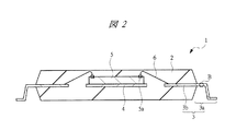
図2は、図1のA−A線で切断した断面を示す断面図である。図2に示すように、リード3は、樹脂2の側面から突出しているアウターリード3aと樹脂2の内部に形成されているインナーリード3bから構成されている。左右のインナーリード3bで挟まれた(複数のインナーリード3bで囲まれた)中央部には、タブ4が形成されており、このタブ4上に半導体チップ5が配置されている。半導体チップ5には、MISFET(Metal Insulator Semiconductor Field Effect Transistor)などの回路素子や配線が形成されており、最上層にボンディングパッド5aが形成されている。ボンディングパッド5a上は、ワイヤ6と接続されており、このワイヤ6はインナーリード3bに接続されている。
2 is a cross-sectional view showing a cross section taken along line AA of FIG. As shown in FIG. 2, the
図3は、図2の領域Bを拡大した図である。すなわち、図3は、樹脂2から露出しているリード3(アウターリード3a)を拡大した断面図である。図3に示すように、リード3の表面(裏面も含む)には、めっき膜10が形成されている。リード3は銅を主材料として構成されており、めっき膜10は、錫を主材料とし、かつ、鉛を含有しない膜から形成されている。このようにリード3には、めっき膜10が形成されているが、リード3の表面にめっき膜10を形成するのは、例えば、以下に示す理由による。
FIG. 3 is an enlarged view of region B of FIG. 3 is an enlarged cross-sectional view of the lead 3 (
図1に示す半導体装置1は、実装基板上に実装されるが、このとき、実装基板上に形成されている端子と半導体装置1に形成されているリード3が電気的に接続される。この端子とリード3との電気的な接続には、半田が用いられる。したがって、銅よりなるリード3を直接端子と半田で接続することも可能であるが、リード3の半田に対する濡れ性を向上させるために、リード3の表面にめっき膜10が形成されるのである。このようにリード3の表面にめっき膜10を形成することにより、リード3と半田との間の濡れ性が向上し、半田を介したリード3と実装基板上の端子との接続信頼性を向上することができる。めっき膜10には、半田との濡れ性が良好な錫を主材料とする膜が使用される。さらに、リード3の表面にめっき膜10を形成することにより、リード3の腐食防止および酸化防止を図ることができる。
The
半導体装置1は、動作環境に応じて室温より高温な状態と常温より低温な状態との熱サイクルにさらされる。つまり、半導体装置1には、熱負荷が加えられる。ここで、リード3の表面にめっき膜10が形成されているが、リード3は銅を主成分とする一方、めっき膜10は錫を主材料としている。したがって、銅と錫とは線膨張係数が異なることから、半導体装置1に熱サイクルが加えられると、銅と錫に応力が働くことになる。例えば、銅の線膨張係数は17.2×10⁻⁶K−1であり、一般的な錫の線膨張係数は24.3×10⁻⁶K−1である。このように、一般的な錫の線膨張係数は、銅の線膨張係数に比べて高くなっている。例えば、半導体装置1が高温状態に置かれると、リード3を構成する銅の膨張よりも、めっき膜10を構成する錫の膨張が大きくなる。このため、めっき膜10には、リード3よりも膨張しようとするが、リード3による銅の膨張がこれについていくことができないため、めっき膜10には、リード3からの拘束により圧縮応力が生じることになる。このように錫の一般的な線膨張係数が銅の線膨張係数に比べて大きいので、高温時に、めっき膜10に圧縮応力が働くことになる。さらに、この高温状態では結晶を構成する原子が熱拡散により拡散しやすい傾向があるため、圧縮応力がめっき膜10に加わると、めっき膜10に針状結晶(ウィスカー)が形成されやすくなる。つまり、めっき膜10からウィスカーが突き出ることになる。このウィスカーの長さは、例えば、数十μmから数百μmにもなる。
The
半導体装置1には、樹脂2から複数のリード3が露出しているが、半導体装置1の小型化および高集積化により、隣接するリード3間の距離が狭くなってきている。このことから、リード3の表面に形成されるめっき膜10にウィスカーが形成されると、ウィスカーによって隣接するリード3が電気的に接続され、半導体装置1にショート不良が発生することになる。したがって、高温時の圧縮応力に起因したウィスカーの発生を防止する必要がある。なお、熱サイクルの低温時には、めっき膜10およびリード3は縮むが、めっき膜10を構成する錫の線膨張係数が、リード3を構成する銅の線膨張係数よりも大きいため、めっき膜10のほうがリード3よりも大きく縮む。このため、めっき膜10には、引張応力が働く。すなわち、熱サイクルの低温時においては、めっき膜10に圧縮応力が働かないので、ウィスカーの発生は問題とならない。以上のことから、熱サイクルの高温時にめっき膜10に発生するウィスカーを防止する必要があることがわかる。
In the
従来技術としてウィスカーの発生を抑制するため、錫を主材料とするめっき膜に鉛を添加することが行なわれてきている。詳細なメカニズムは不明であるが、鉛をめっき膜に含有させることで、めっき膜におけるウィスカーの発生を防止することができるのである。 In order to suppress the occurrence of whiskers as a prior art, lead has been added to a plating film containing tin as a main material. Although the detailed mechanism is unknown, the generation of whiskers in the plating film can be prevented by containing lead in the plating film.
しかし、近年、鉛は環境に流出すると有害になることから、様々な製品の無鉛化が進められ、半導体装置においても無鉛化が要求されてきている。したがって、ウィスカーの発生を抑制するために、錫を主材料とするめっき膜に鉛が添加されてきたが、近年では、鉛をめっき膜に添加しない傾向が強まってきている。このような鉛フリーの傾向化に伴い、錫を主成分とするめっき膜に再びウィスカーの発生が問題として顕在化してきている。 However, in recent years, since lead becomes harmful when it flows into the environment, various products have been made lead-free and semiconductor devices have been required to be lead-free. Accordingly, lead has been added to the plating film mainly composed of tin in order to suppress the generation of whiskers. However, in recent years, there is an increasing tendency that lead is not added to the plating film. With such a trend toward lead-free, the occurrence of whiskers has become apparent as a problem in the plating film containing tin as a main component.
そこで、本実施の形態1では、錫を主成分とし、かつ、鉛を含有しないめっき膜10に生じるウィスカーを以下に示す点に着目して防止している。この点について説明する。まず、ウィスカーの発生原因は、熱サイクルの高温時にめっき膜10に発生する圧縮応力が原因である。そして、この圧縮応力は、めっき膜10の線膨張係数がリード3の線膨張係数よりも大きいことにより生じるものである。このことから、本実施の形態1では、めっき膜10の線膨張係数をリード3の線膨張係数よりも小さくなるように構成している。これにより、熱サイクルの高温時において、めっき膜10の膨張よりもリード3の膨張のほうが大きくなり、めっき膜10に圧縮応力ではなく引張応力が働くことになる。したがって、めっき膜10に圧縮応力が働かないことから、高温時の圧縮応力によって、めっき膜10に形成されるウィスカーの発生を防止することができるのである。
Therefore, in the first embodiment, whiskers generated in the
ここで、疑問になるのは、めっき膜10の主材料は錫であり、リード3の主材料は銅であることである。すなわち、一般的な錫の線膨張係数は、銅の線膨張係数に比べて大きくなっている。それにもかかわらず、錫を主材料とするめっき膜10の線膨張係数を、銅を主材料とするリード3の線膨張係数よりも小さくすることが可能なのかが問題となる。錫の結晶構造は、α−Sn構造とβ−Sn構造の2種類がある。α−Sn構造は低温での結晶構造であり、室温付近の半導体装置1の動作温度範囲では、錫の結晶構造はβ−Sn構造をしている。このβ−Sn構造においては、面方位によって線膨張係数が異なるという特徴を有している。本実施の形態1では、錫の結晶構造において、面方位によって線膨張係数が異なるという異方性に着目している。すなわち、錫よりなる一般的なめっき膜は、多結晶構造であり、めっき膜10中に複数の結晶粒(グレイン)を含んでいる。めっき膜に形成されているそれぞれの結晶粒では様々な面方位を向いている。つまり、一般的なめっき膜10は、様々な面方位を向いている結晶粒から形成されていることになる。言い換えれば、めっき膜10を構成する個々の結晶粒がある1つの面方位に揃っている状態(単結晶)にはなっていない。したがって、様々な面方位を向いている結晶粒のそれぞれは、異なる線膨張係数を有しており、これらの結晶粒からなるめっき膜の線膨張係数は、それぞれの結晶粒の線膨張係数を平均化したものになる。つまり、一般的なめっき膜10は、様々な面方位を向いている結晶粒が均等に含まれている膜から形成されていることが前提となっており、24.3×10−6K−1という錫の線膨張係数は、均等に含まれている面方位の異なる結晶粒のそれぞれの線膨張係数を平均化したものとなっている。このことから、錫の結晶では、表面に並行な方向の面方位によって値が異なることになる。本実施の形態1では、めっき膜10の表面に並行な方向の面方位が特定の面方位を有している場合に、銅の線膨張係数よりも小さくなる点に着目している。
Here, the question is that the main material of the
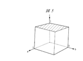
まず、錫の結晶構造を説明する前に面方位の概念について説明する。原子の存在する結晶面の位置と方向とは、その結晶面上の一直線上にない3点によって決定される。この3点の座標を格子定数a1、a2、a3を単位として与えることにより、結晶面を決定することができる。この結晶面は、以下に示す規則により決定された指数(インデックス)によって面の方向を表すことができる。すなわち、結晶面が結晶軸を切り取る長さを格子定数a1、a2、a3を単位として表す。そして、格子定数a1、a2、a3を単位として表した数の逆数を求め、同じ比をなす3個の整数に簡約する。その結果を括弧でくくって(hkl)とし、この(hkl)を結晶面の面指数とする。これにより、(hkl)が結晶面を示すことになる。 First, the concept of the plane orientation will be explained before explaining the crystal structure of tin. The position and direction of the crystal plane in which atoms are present are determined by three points that are not on a straight line on the crystal plane. By giving the coordinates of these three points in units of lattice constants a 1 , a 2 , and a 3 , the crystal plane can be determined. This crystal plane can represent the direction of the plane by an index determined by the following rules. That is, the length by which the crystal plane cuts the crystal axis is expressed in units of lattice constants a 1 , a 2 , and a 3 . Then, the reciprocal of the number expressed in units of the lattice constants a 1 , a 2 , and a 3 is obtained and reduced to three integers having the same ratio. The result is enclosed in parentheses (hkl), and this (hkl) is the plane index of the crystal plane. Thereby, (hkl) indicates a crystal plane.
具体的に(hkl)で特定される結晶面の一例について説明する。図4は、ある結晶面を示す図である。図4において、この面は、結晶軸aとは3a1で交わる。同様に結晶軸bとは2a2で交わり、結晶軸cとは2a3で交わっている。したがって、この結晶面が結晶軸を切り取る長さを格子定数a1、a2、a3で表すと、(3、2、2)となる。この数の組の逆数は、(1/3、1/2、1/2)である。したがって、この逆数の組と同じ比をもつ最小の整数の組は、(2、3、3)となる。このことから、この結晶面の指数は(233)となる。 A specific example of the crystal plane specified by (hkl) will be described. FIG. 4 is a diagram showing a certain crystal plane. In FIG. 4, this plane intersects the crystal axis a at 3a 1 . Similarly, the crystal axis b intersects with 2a 2 and the crystal axis c intersects with 2a 3 . Therefore, when the length of the crystal plane cutting the crystal axis is represented by lattice constants a 1 , a 2 , and a 3 , (3, 2, 2) is obtained. The reciprocal of this number set is (1/3, 1/2, 1/2). Therefore, the smallest integer set having the same ratio as this reciprocal set is (2, 3, 3). From this, the index of this crystal plane is (233).
さらに、(hkl)で特定される結晶面の例について説明する。図5は立方格子の(001)面を示している。すなわち、斜線で示す結晶面は、結晶軸aとは交わらないので、結晶軸aとは∞a1で交わるということができる。同様に結晶軸bとは交わらないので、結晶軸bと∞a2で交わり、結晶軸cとは1a3で交わっている。したがって、この結晶面が結晶軸を切り取る長さを格子定数a1、a2、a3で表すと、(∞、∞、1)となる。この数の組の逆数は、(1/∞(=0)、1/∞(=0)、1)である。したがって、この逆数の組と同じ比をもつ最小の整数の組は、(0、0、1)となる。このことから、この結晶面の指数は(001)となる。 Further, an example of the crystal plane specified by (hkl) will be described. FIG. 5 shows the (001) plane of a cubic lattice. That is, the crystal plane indicated by the oblique lines does not intersect with the crystal axis a, and thus can be said to intersect with the crystal axis a at ∞a 1 . Similarly, since it does not intersect with the crystal axis b, it intersects with the crystal axis b at ∞a 2 and intersects with the crystal axis c at 1a 3 . Therefore, when the length of the crystal plane cutting the crystal axis is represented by lattice constants a 1 , a 2 , and a 3 , (∞, ∞, 1) is obtained. The reciprocal of this set of numbers is (1 / ∞ (= 0), 1 / ∞ (= 0), 1). Therefore, the smallest integer set having the same ratio as this reciprocal set is (0, 0, 1). Therefore, the index of this crystal plane is (001).
図6は立方格子の(110)面を示している。すなわち、斜線で示す結晶面は、結晶軸aとは1a1で交わるということができる。同様に結晶軸bとは1a2で交わり、結晶軸cとは交わらないので、結晶軸cとは∞a3で交わっているということができる。したがって、この結晶面が結晶軸を切り取る長さを格子定数a1、a2、a3で表すと、(1、1、∞)となる。この数の組の逆数は、(1、1、1/∞(=0))である。したがって、この逆数の組と同じ比をもつ最小の整数の組は、(1、1、0)となる。このことから、この結晶面の指数は(110)となる。 FIG. 6 shows the (110) plane of a cubic lattice. That is, the crystal plane shown with diagonal lines, it can be said that intersect at 1a 1 is the crystal axis a. Similarly, since it intersects with the crystal axis b at 1a 2 and does not intersect with the crystal axis c, it can be said that it intersects with the crystal axis c at ∞a 3 . Therefore, when the length of the crystal plane cutting off the crystal axis is represented by lattice constants a 1 , a 2 , and a 3 , (1, 1, ∞) is obtained. The reciprocal of this set of numbers is (1, 1, 1 / ∞ (= 0)). Therefore, the smallest integer set having the same ratio as this reciprocal set is (1, 1, 0). Therefore, the index of this crystal plane is (110).
以上のようにして、結晶面を整数の組による指数(hkl)で表すことができることがわかる。続いて、錫の結晶構造について説明する。図7は、錫のβ−Sn構造を示す図である。図7に示すように、β−Sn構造は複雑な構造をしている。そして、結晶軸a方向の格子定数と結晶軸b方向の格子定数は5.832Åとなっており、結晶軸c方向の格子定数は3.181Åとなっている。図7に示す結晶構造では、例えば、(hkl)面として、(001)、(101)、(220)、(211)、(112)、(321)、(420)、(411)、(312)など様々な面方位が存在する。このように複数の異なる面方位を有するβ−Sn構造では、それぞれの面方位で結晶軸方向の線膨張係数が異なっている。 As described above, it can be seen that the crystal plane can be represented by an index (hkl) based on a set of integers. Next, the crystal structure of tin will be described. FIG. 7 is a view showing a β-Sn structure of tin. As shown in FIG. 7, the β-Sn structure has a complicated structure. The lattice constant in the crystal axis a direction and the lattice constant in the crystal axis b direction are 5.832 、, and the lattice constant in the crystal axis c direction is 3.181 Å. In the crystal structure shown in FIG. 7, for example, as the (hkl) plane, (001), (101), (220), (211), (112), (321), (420), (411), (312) ) And other surface orientations. As described above, in the β-Sn structure having a plurality of different plane orientations, the linear expansion coefficients in the crystal axis direction are different in each plane orientation.
この例を図8に示す。図8における線膨張係数αx、αy、αzは、それぞれ、x軸方向、y軸方向、z軸方向における線膨張係数を示している。ここで、xyz座標系は、結晶軸a、b、cによる座標系と異なる座標系である。すなわち、結晶軸a、b、cによる座標系は、結晶面の面方位を決定する座標系であり、xyz座標系はxy平面をリード3の表面に対応させた座標系である。
An example of this is shown in FIG. The linear expansion coefficients α x , α y , and α z in FIG. 8 indicate the linear expansion coefficients in the x-axis direction, the y-axis direction, and the z-axis direction, respectively. Here, the xyz coordinate system is a coordinate system different from the coordinate system based on the crystal axes a, b, and c. That is, the coordinate system based on the crystal axes a, b, and c is a coordinate system that determines the plane orientation of the crystal plane, and the xyz coordinate system is a coordinate system in which the xy plane corresponds to the surface of the
図8は、それぞれの面方位での結晶軸方向の線膨張係数(単位×10−6K−1)を示す表である。例えば、面方位(001)がxy平面に並行するような結晶構造の場合、x軸方向の線膨張係数αxは15.80(×10−6K−1)であり、y軸方向の線膨張係数αyは15.80(×10−6K−1)である。また、z軸方向の線膨張係数αzは28.40(×10−6K−1)である。したがって、xy面内での線膨張係数の平均値α(=(α1+α2)/2)は15.80(×10−6K−1)であり、銅の線膨張係数17.2(×10−6K−1)よりも小さくなることがわかる。このことから、錫の(001)面をリード3の表面に並行になるように錫を形成することにより、めっき膜10の面内方向(xy平面)の線膨張係数を、リード3を構成する銅の線膨張係数よりも小さくすることができる。つまり、リード3の表面と並行な面を(001)面とする錫の単結晶でめっき膜10を構成することにより、めっき膜10の面内方向の線膨張係数をリード3の面内方向の線膨張係数よりも小さくすることできる。これにより、めっき膜10を形成したリード3に高温の熱負荷がかかった状態でも、めっき膜10に圧縮応力が働かず、めっき膜10でのウィスカーの発生を防止することができる。
FIG. 8 is a table showing the linear expansion coefficient (unit × 10 −6 K −1 ) in the crystal axis direction at each plane orientation. For example, in the case of a crystal structure in which the plane orientation (001) is parallel to the xy plane, the linear expansion coefficient α x in the x-axis direction is 15.80 (× 10 −6 K −1 ), and the line in the y-axis direction The expansion coefficient α y is 15.80 (× 10 −6 K −1 ). The linear expansion coefficient αz in the z-axis direction is 28.40 (× 10 −6 K −1 ). Therefore, the average value α (= (α1 + α2) / 2) of the linear expansion coefficient in the xy plane is 15.80 (× 10 −6 K −1 ), and the linear expansion coefficient of copper is 17.2 (× 10 − It can be seen that it is smaller than 6 K −1 ). From this, the
これに対し、面方位(220)がxy平面に並行するような結晶構造の場合、x軸方向の線膨張係数αxは15.80(×10−6K−1)であり、y軸方向の線膨張係数αyは28.40(×10−6K−1)である。また、z軸方向の線膨張係数αzは15.80(×10−6K−1)である。したがって、xy面内での線膨張係数の平均値αは22.10(×10−6K−1)であり、銅の線膨張係数17.2(×10−6K−1)よりも大きくなってしまうことがわかる。このことから、錫の(220)面をリード3の表面に並行になるように錫を形成することでは、めっき膜10の面内方向(xy平面)の線膨張係数を、リード3を構成する銅の線膨張係数よりも小さくすることはできなくなる。
On the other hand, when the crystal orientation is such that the plane orientation (220) is parallel to the xy plane, the linear expansion coefficient α x in the x-axis direction is 15.80 (× 10 −6 K −1 ), and the y-axis direction The linear expansion coefficient α y is 28.40 (× 10 −6 K −1 ). The linear expansion coefficient αz in the z-axis direction is 15.80 (× 10 −6 K −1 ). Therefore, the average value α of the linear expansion coefficient in the xy plane is 22.10 (× 10 −6 K −1 ), which is larger than the linear expansion coefficient 17.2 (× 10 −6 K −1 ) of copper. It turns out that it will become. Therefore, by forming tin so that the (220) plane of tin is parallel to the surface of the
このようにリード3の表面に並行する面方位によって、めっき膜10の面内方向(xy平面)の線膨張係数が異なる数値になることがわかる。したがって、図8に示す表から、面方位(001)、(101)、(112)などをリード3の表面に並行するような結晶構造でめっき膜10を形成することにより、めっき膜10の面内方向の線膨張係数をリード3の線膨張係数よりも小さくすることができる。特に、(001)面がリード3の表面に並行するような結晶構造では、めっき膜10の面内方向(xy平面)の線膨張係数が最も小さくなることから、めっき膜10の面内方向の線膨張係数をリード3の線膨張係数よりも小さくする観点からは望ましい結晶構造であることがわかる。
Thus, it can be seen that the linear expansion coefficient in the in-plane direction (xy plane) of the
以上のことをまとめると、以下に示すようになる。図9は、リード3の断面を示す断面図である。図9に示すように、リード3の表面にめっき膜10が形成されている。このとき、リード3の表面をxy面とする座標系をとるとき、このxy平面と並行する錫の面方位を特定の面方位とすることにより、めっき膜10の面内方向の線膨張係数をリード3の線膨張係数よりも小さくすることが本実施の形態1における特徴の1つである。銅の結晶構造は、錫の結晶構造のように線膨張係数の異方性は存在しないことから、銅を主材料とするリード3の線膨張係数は、17.2×10⁻⁶K−1である。これに対し、めっき膜10を構成する錫は、線膨張係数の異方性が存在する。したがって、例えば、xy面と並行する錫の面方位を(001)面とすることにより、錫のめっき膜10の面内方向における線膨張係数が15.80(×10−6K−1)となるので、めっき膜10の面内方向の線膨張係数をリード3の線膨張係数よりも小さくすることができるのである。すなわち、めっき膜10を構成する結晶構造として、リード3の表面(xy面)と並行する錫の面方位が(001)面である単結晶とすることで、めっき膜10の面内方向の線膨張係数をリード3の線膨張係数よりも小さくすることができる。ここでは、リード3の表面(xy面)と並行する錫の面方位が(001)面である単結晶について説明しているが、リード3の表面(xy面)と並行する錫の面方位が(101)面や(112)面のようにxy方向の線膨張係数が銅の線膨張係数よりも小さくなる単結晶でも同様の効果が得られる。
The above is summarized as follows. FIG. 9 is a cross-sectional view showing a cross section of the
上記では、例えば、リード3の表面(xy面)と並行する錫の面方位が(001)面である単結晶からめっき膜10を構成する例について説明しているが、めっき膜10を錫の単結晶から構成するのではなく多結晶から構成する場合にも一定条件のもと、めっき膜10の面内方向の線膨張係数をリード3の線膨張係数よりも小さくすることができる。
In the above description, for example, an example in which the
図10は、めっき膜10を錫の多結晶から構成する例を示している。この場合、図10に示すように、リード3の表面(xy面)と並行する錫の面方位が(001)、(101)、(220)、(211)、(312)などとなっている結晶粒からめっき膜10が形成されている。このとき、めっき膜10の体積中、(hkl)面がめっき膜10の表面と並行である結晶粒が占める割合をx(hkl)、めっき膜10の面内方向(xy面)における線膨張係数の平均値をα(hkl)としたとき、めっき膜10の全体の線膨張係数は、x(h1k1l1)×α(h1k1l1)+x(h2k2l2)×α(h2k2l2)+・・・+x(hnknln)×α(hnknln)と見積もることができる。そこで、不等式x(h1k1l1)×α(h1k1l1)+x(h2k2l2)×α(h2k2l2)+・・・+x(hnknln)×α(hnknln)≦17.2×10⁻⁶(銅の線膨張率)を満たすようにめっき膜10を形成することにより、めっき膜10の面内方向の線膨張係数は銅の線膨張係数よりも小さくなる。ただし、上述した不等式において、x(h1k1l1)+x(h2k2l2)+・・・+x(hnknln)=1を満たしている。
FIG. 10 shows an example in which the
したがって、上述した不等式を満たす多結晶からめっき膜10を形成することにより、高温時にめっき膜10に圧縮応力が生じることはないので、めっき膜10にウィスカーが発生することを防止できる。特に、(001)面がめっき膜10の表面と並行である結晶粒では、めっき膜10の表面内における線膨張係数(平均値)が一番小さくなることから、この構造を有する結晶粒が上述した不等式を満たす条件に最も効果的な結晶粒であることがわかる。以上のことから、(001)面、(112)面や(101)面がめっき膜10の表面に並行である結晶粒が、めっき膜10内になるべく多く存在するようにめっき膜10を形成することにより、上述した不等式による条件を満たすめっき膜10を形成することができる。
Therefore, by forming the
次に、めっき膜10の(001)面がリード3の面内方向と並行するように、めっき膜10を形成する方法について説明する。図11に示すように、リード3の表面にまず、電界めっき法により金膜11を形成する。その後、金膜11上に電解めっき法で錫を主材料とするめっき膜10を形成する。このように錫を主材料とするめっき膜10とリード3との間に金膜11を形成することにより、めっき膜10の(001)面がリード3の面内方向と並行するように形成することができる。
Next, a method of forming the
以下に、金膜11上にめっき膜10を形成することにより、めっき膜10の(001)面がリード3の面内方向と並行するように形成できるメカニズムについて説明する。図12は、リード3の表面に形成された金原子12を示す平面図である。図12に示すように、リード3の表面に電界めっき法により金原子12よりなる金膜が形成される。このとき、金膜は、(001)面がリード3の表面に並行になるように形成される。すなわち、図12には、金膜の(001)面を構成する金原子12が配置されている。このように、(001)面がリード3の表面に並行するように金膜を形成するには、金膜を形成する電界めっき法において、電流値、温度およびめっき液の組成を調整することなどにより実現できる。例えば、電界めっき法による金膜の形成を中庸過電圧の条件で行なうことにより、リード3の表面に(001)面が並行するように金原子12を形成することができる。この方法の詳細は、例えば、参考文献(Journal of Electroanalytical Chemistry、9巻、70ページ、1965年)に記載されている。
Hereinafter, a mechanism that allows the (001) plane of the
図12において、金膜の(001)面を構成する金原子12の格子定数は4.0785Åであり、図12に示す間隔Lの距離は5.768Åとなっている。続いて、この金膜上に錫原子を形成する。図13は、錫を主材料とするめっき膜の(001)面での錫原子13の配列を示す図である。(001)面内の錫原子13の格子定数は5.832Åである。したがって、図12に示す間隔L(5.768Å)と、図13に示す錫原子13の格子定数(5.832Å)とは、ほぼ等しい値を有することから、金膜の(001)面上に錫の(001)面が成長しやすくなる。つまり、金膜の(001)面と錫の(001)面との界面では、図14に示すように金原子12と錫原子13が配列される。
In FIG. 12, the lattice constant of the
図14に示すように、金膜上に錫を主材料とするめっき膜を形成する場合には、(001)面を構成するように金原子12が配列されており、この金原子12で満たされていない空間にちょうどはまるように錫原子13が配置されていくことになる。このとき、錫原子13が金原子12の配置されていないスペースに配置されるが、このスペースの間隔Lが錫の(001)面の格子定数とほぼ等しくなる。このことから、自然と金膜上には(001)面がリード3の表面に並行するように錫原子13が成長することになる。つまり、(001)面を有する金膜上には錫の(001)面が成長しやすい状況になっている。このように金膜の(001)面がリード3の表面に並行になるように金膜を形成すると、金原子の配列構成および錫における(001)面の格子定数の関係から、金膜上に錫の(001)面が形成されやすくなるという点を見出したことに本実施の形態1の特徴の1つがある。これにより、金膜を介してリード3上に錫の(001)面がリード3の表面と並行するめっき膜を形成することができるのである。
As shown in FIG. 14, in the case where a plating film containing tin as a main material is formed on a gold film,
本実施の形態1では、錫を主材料とするめっき膜とリードとの間に金膜を形成する例について説明したが、金膜の他に銀膜を形成するようにしてもよい。すなわち、銀膜の(001)面も金膜の(001)面と同等な構成をしており、格子間隔も似ている。したがって、銀膜上に錫を主材料とするめっき膜を形成する場合、銀原子の配置されていないスペースに錫原子が配置されるようになる。このとき、スペースの間隔が錫の(001)面の格子定数とほぼ等しくなる点が金膜の場合と同様である。このことから、自然と銀膜上には(001)面がリード3の表面に並行するように錫原子13を成長させることができる。
In the first embodiment, the example in which the gold film is formed between the plating film containing tin as a main material and the lead has been described, but a silver film may be formed in addition to the gold film. That is, the (001) plane of the silver film has the same configuration as the (001) plane of the gold film, and the lattice spacing is similar. Therefore, when forming a plating film containing tin as a main material on a silver film, tin atoms are arranged in a space where silver atoms are not arranged. At this time, the point that the space interval is almost equal to the lattice constant of the (001) plane of tin is the same as in the case of the gold film. Therefore,
また、金膜はリード全体を覆うように形成する必要はなく、部分的にリード上に形成されていてもよい。これは、金膜は、錫の(001)面がリードの表面に並行になるように形成するために用いられるからである。すなわち、錫を主成分とするめっき膜が、リードの表面と並行する面方位の異なる複数の結晶粒から構成される場合(多結晶の場合)には、(001)面がリードの表面に並行になる結晶粒が形成される領域に金膜が形成されていればよいからである。 The gold film does not need to be formed so as to cover the entire lead, and may be partially formed on the lead. This is because the gold film is used so that the (001) plane of tin is parallel to the surface of the lead. That is, when the plating film mainly composed of tin is composed of a plurality of crystal grains having different plane orientations parallel to the lead surface (in the case of polycrystal), the (001) plane is parallel to the lead surface. This is because a gold film may be formed in a region where the crystal grains to be formed are formed.
さらに、めっき膜が完成した後に加熱処理が実施され、金膜を構成する金原子がリードを構成する銅あるいはめっき膜を構成する錫の内部に拡散することで消滅しても問題はない。金膜は、錫の(001)面がリードの表面に並行になるように形成するために用いられる膜であり、金膜が消滅しても、めっき膜が完成した後は、錫の(001)面がリードの表面に並行になっている状態を維持するからである。したがって、完成した半導体装置においては、リード上に金膜を形成したにもかかわらず、リード上には金膜が存在せず直接錫を主材料とするめっき膜が形成されている構造になっている場合もある。 Furthermore, heat treatment is performed after the plating film is completed, and there is no problem even if gold atoms constituting the gold film disappear by diffusion into the copper constituting the lead or tin constituting the plating film. The gold film is a film used for forming the (001) surface of tin so as to be parallel to the surface of the lead. Even if the gold film disappears, the (001) surface of tin is not used after the plating film is completed. This is because the surface is maintained parallel to the surface of the lead. Therefore, the completed semiconductor device has a structure in which a gold film is formed on the lead, but a gold film is not present on the lead and a plating film mainly made of tin is directly formed. There may be.
次に、本実施の形態1における半導体装置の製造方法について説明する。本実施の形態1のパッケージ形態としてQFPについて説明したが、以下に示す製造方法ではQFPと同じ表面実装型のパッケージ形態であるSOP(Small Outline Package)について説明する。パッケージ形態がQFPやSOPであっても基本的な製造工程は同様である。 Next, a method for manufacturing the semiconductor device according to the first embodiment will be described. Although QFP has been described as the package form of the first embodiment, SOP (Small Outline Package), which is the same surface mount type package form as QFP, will be described in the following manufacturing method. The basic manufacturing process is the same even if the package form is QFP or SOP.
まず、図15において、半導体ウェハ20を用意する。半導体ウェハ20は複数のチップ領域に区分けされており、複数のチップ領域のそれぞれにLSI(Large Scale Integration Circuit)が形成されている。LSIはいわゆるウェハプロセス(前工程)で形成される。
First, in FIG. 15, a
続いて、ブレード21によって半導体ウェハ20を切断する。すなわち、半導体ウェハ20をチップ領域単位で切断することにより、半導体チップを取得する。一方、半導体チップを搭載するためのリードフレームを用意する。このリードフレーム22は、例えば、銅を主材料としている。続いて、リードフレームに形成されているリードの表面にめっき膜を形成する。このめっき工程で本実施の形態1における技術的思想が具現化される。例えば、上述したように、リードの表面にまず、電界めっき法により金膜を形成する。その後、金膜上に電解めっき法で錫を主材料とするめっき膜を形成する。このように錫を主材料とするめっき膜とリードとの間に金膜を形成することにより、めっき膜の(001)面がリードの面内方向と並行するように形成することができる。このめっき方法によりめっき膜は、(001)面がリードの面内方向と並行する単結晶状態の錫や、あるいは、上述した不等式x(h1k1l1)×α(h1k1l1)+x(h2k2l2)×α(h2k2l2)+・・・+x(hnknln)×α(hnknln)≦17.2×10⁻⁶(銅の線膨張率)を満たす多結晶状態の錫から形成することができる。
Subsequently, the
そして、図16に示すように、めっき処理したリードパターンが形成されているリードフレーム22のタブ上に半導体チップ20aを搭載する。半導体チップ20aは、ダイボンダによりリードフレーム22に形成されているタブ上に搭載される。
Then, as shown in FIG. 16, the
次に、図17に示すように、タブ上に搭載した半導体チップ20aに形成されているパッド(図示せず)と、リードフレーム22に形成されている複数のリード(インナーリード)とをワイヤ23により接続する。ワイヤ23はキャピラリを使用することによりパッドとリードとを接続する。
Next, as shown in FIG. 17, a pad (not shown) formed on the
その後、図18に示すように、リードフレーム22に搭載された半導体チップ20aとインナーリードを含む領域を樹脂24によって封止する。樹脂24による封止は、半導体チップ20aを外力による衝撃や水分の浸入から保護するために行なわれる。
Thereafter, as shown in FIG. 18, the region including the
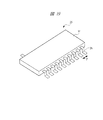
次に、リードフレーム22から樹脂24で封止した封止体を個片化する。これにより、図19に示す半導体装置25を得ることができる。半導体装置25は、樹脂24による封止体と、この封止体から突出しているリード(アウターリード)26から構成される。そして、封止体から突出しているリード26の表面にめっき膜(図示せず)が形成されている。
Next, the sealing body sealed with the
本実施の形態1によれば、リード26の表面に形成されるめっき膜(錫)の面内方向の線膨張係数をリード26(銅)の線膨張係数よりも小さくすることができる。したがって、めっき膜を形成したリード26に高温の熱負荷がかかった状態でも、めっき膜に圧縮応力が働かず、めっき膜でのウィスカーの発生を防止することができる。一方、めっき膜(錫)の面内方向の線膨張係数をリード26(銅)の線膨張係数よりも小さくすると、低温の熱負荷が加わった場合に、めっき膜に圧縮応力が働くことになる。しかし、低温時には原子の拡散が起こりにくくなるので、圧縮応力によるウィスカーは発生しない。すなわち、低温時の圧縮応力はウィスカー発生の問題とはならない。
According to the first embodiment, the in-plane linear expansion coefficient of the plating film (tin) formed on the surface of the
以上のことから、本実施の形態1における半導体装置25によれば、リード26の表面に形成されためっき膜でのウィスカーの発生を防止することができる。ウィスカーが発生する場合には、隣接するリード26間の間隔Pを狭くすると、ウィスカーを介して隣接するリード26が電気的に接続され半導体装置25にショート不良が発生してしまう。これに対し、本実施の形態1では、リード26の表面に形成されているめっき膜にウィスカーが発生しないので、隣接するリード26間の間隔Pを狭くすることができる。例えば、隣接するリード26間の間隔Pを0.5mm以下とすることができ、半導体装置25の多ピン化あるいは小型化を図ることができる。このようにして、本実施の形態1における半導体装置25を製造することができる。
From the above, according to the
本実施の形態1の特徴の1つは、錫を主材料とするめっき膜の面内方向における線膨張係数を、リードを構成する銅の線膨張係数よりも小さくする点にある。この構造を実際に具現化する1つの方法として、めっき膜の面内方向に並行する錫の面方位を特定の面方位にすることで実現している。例えば、めっき膜を錫の多結晶から形成する場合は、上述した不等式x(h1k1l1)×α(h1k1l1)+x(h2k2l2)×α(h2k2l2)+・・・+x(hnknln)×α(hnknln)≦17.2×10⁻⁶(銅の線膨張率)を満たすように個々の結晶粒を形成する必要がある。このようにめっき膜を錫の多結晶から形成する場合に、本実施の形態1による構成が使用されているかについては、何らかの確認手法が必要となる。以下では、検証対象となるめっき膜が本当に上述した不等式を満たしているかについて確認する方法について説明する。 One of the features of the first embodiment is that the linear expansion coefficient in the in-plane direction of the plating film containing tin as a main material is made smaller than the linear expansion coefficient of copper constituting the lead. As one method for actually realizing this structure, it is realized by setting the plane orientation of tin parallel to the in-plane direction of the plating film to a specific plane orientation. For example, when the plating film is formed from a polycrystal of tin, the above-described inequality x (h 1 k 1 l 1 ) × α (h 1 k 1 l 1 ) + x (h 2 k 2 l 2 ) × α (h 2 k 2 l 2 ) +... + X (h n k n l n ) × α (h n k n l n ) ≦ 17.2 × 10 −6 (copper linear expansion coefficient) It is necessary to form crystal grains. Thus, when the plating film is formed from tin polycrystal, some confirmation technique is required as to whether the configuration according to the first embodiment is used. Below, the method to confirm whether the plating film used as verification object really satisfy | fills the inequality mentioned above is demonstrated.
結晶構造の解析には一般的にX線回折測定が使用される。X線回折測定とは、結晶にX線を入射させると、規則的に配置されている個々の原子によってX線が回折され、この回折現象によって結晶から出射されたX線の強度がある場所では強め合う一方、他のある場所では弱め合うという強弱が出る。この強弱を観測することにより結晶構造を解析することができる。 An X-ray diffraction measurement is generally used for the analysis of the crystal structure. In X-ray diffraction measurement, when X-rays are incident on a crystal, the X-rays are diffracted by the regularly arranged individual atoms, and the X-rays emitted from the crystal by this diffraction phenomenon are in places where the intensity is high. While strengthening each other, there is the strength of weakening each other. The crystal structure can be analyzed by observing this strength.
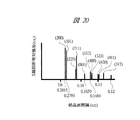
図20は、複数の面方位がランダムに存在する粉末状態の錫結晶についてX線回折測定を行なった結果である。図20において、横軸は結晶面間隔を示しており、縦軸はX線回折相対強度を示している。図20に示すように、X線回折相対強度には複数のピークからなるスペクトルが検出されている。このスペクトルが検出される結晶面間隔を調べることにより、このスペクトルがどの面方位を示しているかがわかる。粉末状態の錫結晶では、面方位の異なる結晶粒が同等に含まれていることを前提としている。したがって、図20では、それぞれのスペクトルの大きさが異なっているが、これは、ある面方位を有する結晶粒が多く含まれているということを示しているものではない。すなわち、面方位によって検出されるスペクトルの大きさが異なるのである。例えば、(200)面のスペクトル強度は大きくなる傾向があり、(001)面のスペクトル強度は小さくなる傾向があるということがわかる。具体的に、結晶面(面方位)のX線回折相対強度を(200)面の強度を100として表すと、(101)面の強度が90、(220)面の強度が34、(211)面の強度が74、(001)面の強度が17、(112)面の強度が23、(400)面の強度が13、(321)面の強度が20、(420)面の強度が15、(411)面の強度が15、(312)面の強度が20となる。 FIG. 20 shows the results of X-ray diffraction measurement of a powdered tin crystal having a plurality of plane orientations randomly present. In FIG. 20, the horizontal axis indicates the crystal plane spacing, and the vertical axis indicates the X-ray diffraction relative intensity. As shown in FIG. 20, a spectrum composed of a plurality of peaks is detected in the X-ray diffraction relative intensity. By examining the crystal plane spacing at which this spectrum is detected, it can be seen which plane orientation this spectrum shows. In the powdered tin crystal, it is assumed that crystal grains having different plane orientations are equally contained. Therefore, in FIG. 20, the magnitudes of the respective spectra are different, but this does not indicate that many crystal grains having a certain plane orientation are included. That is, the detected spectrum size differs depending on the plane orientation. For example, it can be seen that the spectral intensity of the (200) plane tends to increase and the spectral intensity of the (001) plane tends to decrease. Specifically, when the X-ray diffraction relative intensity of the crystal plane (plane orientation) is expressed with the (200) plane intensity as 100, the (101) plane intensity is 90, the (220) plane intensity is 34, (211) The strength of the surface is 74, the strength of the (001) surface is 17, the strength of the (112) surface is 23, the strength of the (400) surface is 13, the strength of the (321) surface is 20, and the strength of the (420) surface is 15. , (411) plane strength is 15, and (312) plane strength is 20.
次に、図21は、実際にリードに形成されためっき膜についてX線回折測定を行なった結果を示している。図21に示すように、例えば、このめっき膜においては、リードの表面に並行する面方位が(211)面と、(001)面と、(411)面と、(312)面の4つが検出されていることを示している。ただし、図21に示すそれぞれのX線回折相対強度がそれぞれの面方位を有する結晶粒の割合を示しているとはいうことはできない。なぜなら、同じ割合で異なる面方位の結晶粒が含まれていても、図20で説明したようにX線回折相対強度は面方位ごとに異なるからである。したがって、図21に示す測定結果から、面方位が異なる結晶粒の割合を算出するためには、図20に示す測定結果で定量化する必要がある。 Next, FIG. 21 shows the result of X-ray diffraction measurement performed on the plating film actually formed on the lead. As shown in FIG. 21, for example, in this plating film, four plane orientations parallel to the surface of the lead are detected: (211) plane, (001) plane, (411) plane, and (312) plane. It has been shown. However, it cannot be said that the respective X-ray diffraction relative intensities shown in FIG. 21 indicate the proportion of crystal grains having the respective plane orientations. This is because, even if crystal grains having different plane orientations are included at the same ratio, the X-ray diffraction relative intensity differs for each plane orientation as described with reference to FIG. Therefore, in order to calculate the ratio of crystal grains having different plane orientations from the measurement results shown in FIG. 21, it is necessary to quantify the measurement results shown in FIG.
図21の測定結果は(001)面の強度を100とすると、(211)面の強度が7.4、(001)面の強度が100、(411)面の強度が15、(312)面の強度が20となる。これらのデータを図20に示す粉末状態の錫の測定結果で割り算すると、(211)面の強度が7.4/74=0.1、(001)面の強度が100/17=5.88、(411)面の強度が15/15=1、(312)面の強度が20/20=1となる。この割り算した値は、めっき膜に含まれる異なる面方位の結晶粒の割合を示していることになる。さらに4つの面方位におけるX線回折相対強度を合計で1になるように規格化する。つまり、これらの合計である7.98(0.1+5.88+1+1)で割り算することによって、不等式中のx(hkl)を求めることができる。具体的には、x(211)が0.0125、x(001)が0.737、x(411)が0.125、x(312)が0.125となる。そして、図8に示す値を使用することにより、x(211)×α(211)+x(001)×α(001)+x(411)×α(411)+x(312)×α(312)=16.9×10−6と算出され、この値は銅の線膨張率17.2×10−6よりも小さくなることがわかる。以上のようにX線回折相対強度の測定結果を利用することにより、検証対象となるめっき膜が本当に上述した不等式を満たしているかについて確認することができる。上述した例からもわかるように、リードの表面に並行する面方位が(001)面を多く含むめっき膜は、めっき膜の表面内における線膨張係数を小さくする効果がある。リードの表面に並行する面方位が(001)面を多く含むかについて検証するには、X線回折相対強度のピークがより大きくなることによって判別することができる。特に(001)面によるX線回折相対強度のピークが最も高くなると、めっき膜の表面内における線膨張係数を小さくする効果が顕著になる。 The measurement results in FIG. 21 show that the strength of the (001) plane is 100, the strength of the (211) plane is 7.4, the strength of the (001) plane is 100, the strength of the (411) plane is 15, and the (312) plane. The strength of is 20. When these data are divided by the measurement results of powdered tin shown in FIG. 20, the strength of the (211) plane is 7.4 / 74 = 0.1, and the strength of the (001) plane is 100/17 = 5.88. , (411) plane strength is 15/15 = 1, and (312) plane strength is 20/20 = 1. This divided value indicates the ratio of crystal grains having different plane orientations contained in the plating film. Further, the X-ray diffraction relative intensities in the four plane orientations are normalized so as to be 1. That is, x (hkl) in the inequality can be obtained by dividing by 7.98 (0.1 + 5.88 + 1 + 1) which is the sum of these. Specifically, x (211) is 0.0125, x (001) is 0.737, x (411) is 0.125, and x (312) is 0.125. Then, by using the values shown in FIG. 8, x (211) × α (211) + x (001) × α (001) + x (411) × α (411) + x (312) × α (312) = It is calculated as 16.9 × 10 −6, and it can be seen that this value is smaller than the linear expansion coefficient of copper of 17.2 × 10 −6 . As described above, by using the measurement result of the X-ray diffraction relative intensity, it is possible to confirm whether the plating film to be verified really satisfies the above inequality. As can be seen from the above-described example, the plating film whose plane orientation parallel to the surface of the lead includes many (001) planes has an effect of reducing the linear expansion coefficient in the surface of the plating film. In order to verify whether the plane orientation parallel to the surface of the lead includes many (001) planes, it can be determined by the peak of the X-ray diffraction relative intensity becoming larger. In particular, when the peak of the X-ray diffraction relative intensity by the (001) plane becomes the highest, the effect of reducing the linear expansion coefficient in the surface of the plating film becomes remarkable.
結晶構造のひずみによって(001)面に対応するX線回折相対強度の現れる位置は多少ずれることがあるが、結晶面間隔0.16nmから0.18nmの間に現れる。 The position at which the X-ray diffraction relative intensity corresponding to the (001) plane appears is slightly shifted due to the distortion of the crystal structure, but appears between 0.16 nm and 0.18 nm between the crystal planes.
(実施の形態2)
本実施の形態2では、リードの表面上に形成するめっき膜を多層構造にする例について説明する。図22は、本実施の形態2における半導体装置において、リード3上に形成されているめっき膜の構成を示す断面図である。図22において、リード3の表面上には金膜11が形成されており、この金膜11上に錫を主材料とするめっき膜10が形成されている。このめっき膜10が1層目のめっき膜となり、めっき膜10上に、さらに、錫を主材料とするめっき膜15が形成されている。このように本実施の形態2では、金膜11上にめっき膜10とめっき膜15よりなる多層膜が形成されている。
(Embodiment 2)
In the second embodiment, an example in which the plating film formed on the surface of the lead has a multilayer structure will be described. FIG. 22 is a cross-sectional view showing the configuration of the plating film formed on the
このとき、金膜11は金膜11上に形成されるめっき膜10の結晶面(面方位)を特定方向に制御する機能を有している。具体的には、前記実施の形態1で述べたとおり、金膜11の(001)面がリード3の表面に並行になるように形成されており、この金膜11上に形成されるめっき膜10は、錫の(001)面がリード3の表面に並行になるように形成される。
At this time, the
したがって、めっき膜10の面内方向の線膨張係数をリード3の線膨張係数よりも小さくすることができるのである。すなわち、めっき膜10を構成する結晶構造として、リード3の表面と並行する錫の面方位が(001)面である単結晶とすることで、めっき膜10の面内方向の線膨張係数をリード3の線膨張係数よりも小さくすることができる。
Therefore, the linear expansion coefficient in the in-plane direction of the
さらに、めっき膜10を錫の単結晶から構成するのではなく多結晶から構成するようにしてもよい。具体的には、前記実施の形態1と同様に、めっき膜10の体積中、(hkl)面がめっき膜10の表面と並行である結晶粒が占める割合をx(hkl)、めっき膜10の面内方向(xy面)における線膨張係数の平均値をα(hkl)としたとき、めっき膜10の全体の線膨張係数は、x(h1k1l1)×α(h1k1l1)+x(h2k2l2)×α(h2k2l2)+・・・+x(hnknln)×α(hnknln)と見積もることができる。そこで、不等式x(h1k1l1)×α(h1k1l1)+x(h2k2l2)×α(h2k2l2)+・・・+x(hnknln)×α(hnknln)≦17.2×10⁻⁶(銅の線膨張率)を満たすようにめっき膜10を形成することにより、めっき膜10の面内方向の線膨張係数は銅の線膨張係数よりも小さくすることができる。
Furthermore, the
次に、めっき膜10上に形成されるめっき膜15は、めっき膜10と同様の構成をとってもよいし、異なる構成をとってもよい。ただし、めっき膜15も面内方向の線膨張係数が銅の線膨張係数より小さくすることが望ましい。めっき膜15において、例えば、めっき膜15の面内方向の線膨張率が銅の線膨張率よりも大きくなると、めっき膜15に圧縮応力が発生し、ウィスカーの発生原因となるからである。したがって、めっき膜15は、めっき膜10と同様の構成にする必要はないが、上述した不等式を満たす構成をとって、めっき膜15の面内方向の線膨張係数を銅の線膨張係数よりも小さくすることが望ましい。具体的には、めっき膜15もリード3の表面と並行する錫の面方位が(001)面、(101)面、(112)面などである単結晶から構成することや、めっき膜15の表面に並行する面方位が(001)面、(101)面、(112)面などである結晶粒を多く含む多結晶から構成することができる。
Next, the
なお、前記実施の形態1と同様に、金膜11はリード全体を覆うように形成する必要はなく、部分的にリード上に形成されていてもよい。これは、金膜11は、錫の(001)面がリードの表面に並行になるように形成するために用いられるからである。すなわち、錫を主成分とするめっき膜が、リードの表面と並行する面方位の異なる複数の結晶粒から構成される場合(多結晶の場合)には、(001)面がリードの表面に並行になる結晶粒が形成される領域に金膜11が形成されていればよいからである。
As in the first embodiment, the
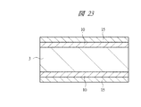
さらに、めっき膜が完成した後に加熱処理が実施され、金膜11を構成する金原子がリード3を構成する銅あるいはめっき膜10を構成する錫の内部に拡散することで消滅しても問題はない。金膜11は、錫の(001)面がリード3の表面に並行になるように形成するために用いられる膜であり、金膜11が消滅しても、めっき膜10が完成した後は、錫の(001)面がリード3の表面に並行になっている状態を維持するからである。したがって、図23に示すように、リード3上に金膜11を形成したにもかかわらず、リード3上には金膜11が存在せず直接錫を主材料とするめっき膜10が形成されている構造になっている場合もある。
Further, the heat treatment is performed after the plating film is completed, and there is a problem even if the gold atoms constituting the
以上、本発明者によってなされた発明を実施の形態に基づき具体的に説明したが、本発明は前記実施の形態に限定されるものではなく、その要旨を逸脱しない範囲で種々変更可能であることはいうまでもない。 As mentioned above, the invention made by the present inventor has been specifically described based on the embodiment. However, the present invention is not limited to the embodiment, and various modifications can be made without departing from the scope of the invention. Needless to say.
本発明は、半導体装置を製造する製造業に幅広く利用することができる。 The present invention can be widely used in the manufacturing industry for manufacturing semiconductor devices.
1 半導体装置
2 樹脂
3 リード
3a アウターリード
3b インナーリード
4 タブ
5 半導体チップ
5a ボンディングパッド
6 ワイヤ
10 めっき膜
11 金膜
12 金原子
13 錫原子
15 めっき膜
20 半導体ウェハ
20a 半導体チップ
21 ブレード
22 リードフレーム
23 ワイヤ
24 樹脂
25 半導体装置
26 リード
a 結晶軸
b 結晶軸
c 結晶軸
L 間隔
P 間隔
DESCRIPTION OF
Claims (14)
(b)前記半導体チップと電気的に接続された、銅を主材料とする複数のリードと、
(c)前記複数のリードのそれぞれの表面に形成されためっき膜であって、錫を主材料とし、かつ、鉛を含有しない前記めっき膜と、
(d)前記半導体チップを封止する封止体とを備え、
前記封止体から前記複数のリードのそれぞれの一部が露出する半導体装置であって、
前記めっき膜の面内方向の線膨張係数が、前記銅の線膨張係数よりも小さいことを特徴とする半導体装置。 (A) a semiconductor chip;
(B) a plurality of leads mainly made of copper, electrically connected to the semiconductor chip;
(C) a plating film formed on the surface of each of the plurality of leads, the plating film containing tin as a main material and not containing lead;
(D) a sealing body for sealing the semiconductor chip;
A semiconductor device in which a part of each of the plurality of leads is exposed from the sealing body,
A semiconductor device, wherein a linear expansion coefficient in an in-plane direction of the plating film is smaller than a linear expansion coefficient of the copper.
前記めっき膜を構成する前記錫は、複数の結晶粒を有する多結晶であり、
前記複数の結晶粒の中には、(001)面が前記めっき膜の表面に並行となる結晶粒が含まれていることを特徴とする半導体装置。 The semiconductor device according to claim 1,
The tin constituting the plating film is a polycrystal having a plurality of crystal grains,
The semiconductor device, wherein the plurality of crystal grains include crystal grains having a (001) plane parallel to the surface of the plating film.
前記めっき膜の体積中、(hkl)面が前記めっき膜の表面と並行である結晶粒が占める割合をx(hkl)、(hkl)面が前記めっき膜の表面と並行である結晶粒の前記めっき膜の面内方向における線膨張係数の平均値をα(hkl)とするとき、x(h1k1l1)×α(h1k1l1)+x(h2k2l2)×α(h2k2l2)+・・・+x(hnknln)×α(hnknln)≦17.2×10⁻⁶(ただし、x(h1k1l1)+x(h2k2l2)+・・・+x(hnknln)=1)を満たすことを特徴とする半導体装置。 The semiconductor device according to claim 2,
In the volume of the plating film, the proportion of crystal grains whose (hkl) plane is parallel to the surface of the plating film is x (hkl), and the crystal grains whose (hkl) plane is parallel to the surface of the plating film When the average value of the linear expansion coefficient in the in-plane direction of the plating film is α (hkl), x (h 1 k 1 l 1 ) × α (h 1 k 1 l 1 ) + x (h 2 k 2 l 2 ) × α (h 2 k 2 l 2 ) +... + X (h n k n l n ) × α (h n k n l n ) ≦ 17.2 × 10 −6 (where x (h 1 k 1 l 1 ) + x (h 2 k 2 l 2 ) +... + x (h n k n l n ) = 1) is satisfied.
前記複数のリードと前記めっき膜の間には金膜が形成されていることを特徴とする半導体装置。 The semiconductor device according to claim 2,
A semiconductor device, wherein a gold film is formed between the plurality of leads and the plating film.
前記金膜は、(001)面が前記めっき膜の表面と並行するように形成されていることを特徴とする半導体装置。 The semiconductor device according to claim 4,
The gold film is formed so that a (001) plane is parallel to the surface of the plating film.
前記めっき膜に対してX線回折を使用することにより結晶構造を解析すると、X線回折による強度ピークは結晶面間隔の値が0.16nmから0.18nmの間に現れることを特徴とする半導体装置。 The semiconductor device according to claim 1,
When a crystal structure is analyzed by using X-ray diffraction for the plating film, an intensity peak due to X-ray diffraction appears between crystal plane spacing values of 0.16 nm to 0.18 nm. apparatus.
結晶面間隔の値が0.16nmから0.18nmの間に現れる強度ピークは、最も高いピークであることを特徴とする半導体装置。 The semiconductor device according to claim 6,
A semiconductor device characterized in that an intensity peak appearing between crystal plane spacing values of 0.16 nm to 0.18 nm is the highest peak.
(b)前記半導体チップと電気的に接続された、銅を主材料とする複数のリードと、
(c)前記複数のリードのそれぞれの表面に形成されためっき膜であって、錫を主材料とし、かつ、鉛を含有しない前記めっき膜と、
(d)前記半導体チップを封止する封止体とを備え、
前記封止体から前記複数のリードのそれぞれの一部が露出する半導体装置であって、
前記めっき膜は、面内方向の線膨張係数が、前記銅の線膨張係数よりも小さい膜を含むことを特徴とする半導体装置。 (A) a semiconductor chip;
(B) a plurality of leads mainly made of copper, electrically connected to the semiconductor chip;
(C) a plating film formed on the surface of each of the plurality of leads, the plating film containing tin as a main material and not containing lead;
(D) a sealing body for sealing the semiconductor chip;
A semiconductor device in which a part of each of the plurality of leads is exposed from the sealing body,
The semiconductor device according to claim 1, wherein the plating film includes a film having a linear expansion coefficient in an in-plane direction smaller than that of the copper.
前記めっき膜に含まれ、面内方向の線膨張係数が前記銅の線膨張係数よりも小さい膜は、前記複数のリードのそれぞれと直接接触していることを特徴とする半導体装置。 9. The semiconductor device according to claim 8, wherein
A film included in the plating film and having a linear expansion coefficient in the in-plane direction smaller than that of the copper is in direct contact with each of the plurality of leads.
(b)前記リードフレームに形成されている複数のリードの表面に、錫を主材料とし、かつ、鉛を含有しないめっき膜を形成する工程と、
(c)前記リードフレームのタブ上に半導体チップを搭載する工程と、
(d)前記半導体チップと、前記リードフレームに形成されている前記複数のリードとをワイヤで接続する工程と、
(e)前記半導体チップを封止して封止体を形成する工程と、
(f)前記リードフレームを切断して前記封止体を個片化する工程とを備え、
前記めっき膜の面内方向の線膨張係数が、前記複数のリードを構成する前記銅の線膨張係数よりも小さくなるように前記めっき膜を形成することを特徴とする半導体装置の製造方法。 (A) preparing a lead frame mainly composed of copper;
(B) forming a plating film containing tin as a main material and not containing lead on the surfaces of a plurality of leads formed on the lead frame;
(C) mounting a semiconductor chip on the tab of the lead frame;
(D) connecting the semiconductor chip and the plurality of leads formed on the lead frame with wires;
(E) sealing the semiconductor chip to form a sealing body;
(F) cutting the lead frame to singulate the sealing body;
A method of manufacturing a semiconductor device, wherein the plating film is formed so that a linear expansion coefficient in an in-plane direction of the plating film is smaller than a linear expansion coefficient of the copper constituting the plurality of leads.
前記めっき膜を構成する前記錫は、複数の結晶粒を有する多結晶であり、
前記複数の結晶粒の中に、(001)面が前記めっき膜の表面に並行となる結晶粒が含まれるように前記めっき膜を形成することを特徴とする半導体装置の製造方法。 A method for manufacturing a semiconductor device according to claim 10, comprising:
The tin constituting the plating film is a polycrystal having a plurality of crystal grains,
The method of manufacturing a semiconductor device, wherein the plating film is formed so that a crystal grain having a (001) plane parallel to the surface of the plating film is included in the plurality of crystal grains.
前記めっき膜の体積中、(hkl)面が前記めっき膜の表面と並行である結晶粒が占める割合をx(hkl)、(hkl)面が前記めっき膜の表面と並行である結晶粒の前記めっき膜の面内方向における線膨張係数の平均値をα(hkl)とするとき、x(h1k1l1)×α(h1k1l1)+x(h2k2l2)×α(h2k2l2)+・・・+x(hnknln)×α(hnknln)≦17.2×10⁻⁶(ただし、x(h1k1l1)+x(h2k2l2)+・・・+x(hnknln)=1)を満たすような前記めっき膜を形成することを特徴とする半導体装置の製造方法。 A method for manufacturing a semiconductor device according to claim 11, comprising:
In the volume of the plating film, the proportion of crystal grains whose (hkl) plane is parallel to the surface of the plating film is x (hkl), and the crystal grains whose (hkl) plane is parallel to the surface of the plating film When the average value of the linear expansion coefficient in the in-plane direction of the plating film is α (hkl), x (h 1 k 1 l 1 ) × α (h 1 k 1 l 1 ) + x (h 2 k 2 l 2 ) × α (h 2 k 2 l 2 ) +... + X (h n k n l n ) × α (h n k n l n ) ≦ 17.2 × 10 −6 (where x (h 1 k 1 l 1) + x (h 2 k 2 l 2) + ··· + x (h n k n l n) = method of manufacturing a semiconductor device characterized by forming the plating film that satisfies 1).
前記(b)工程は、
(b1)前記リードフレームに形成されている前記複数のリードの表面に、金膜を形成する工程と、
(b2)前記(b1)工程後、前記金膜上に、錫を主材料とし、かつ、鉛を含有しない前記めっき膜を形成する工程とを有することを特徴とする半導体装置の製造方法。 A method for manufacturing a semiconductor device according to claim 10, comprising:
The step (b)
(B1) forming a gold film on the surfaces of the plurality of leads formed on the lead frame;
(B2) A method of manufacturing a semiconductor device comprising, after the step (b1), a step of forming the plating film containing tin as a main material and not containing lead on the gold film.
前記(b1)工程は、前記金膜を(001)面が前記めっき膜の表面と並行するような条件で形成することを特徴とする半導体装置の製造方法。 A method for manufacturing a semiconductor device according to claim 13, comprising:
In the step (b1), the gold film is formed under the condition that the (001) plane is parallel to the surface of the plating film.
Priority Applications (8)
| Application Number | Priority Date | Filing Date | Title |
|---|---|---|---|
| JP2007278437A JP2009108339A (en) | 2007-10-26 | 2007-10-26 | Semiconductor device and its fabrication process |
| KR1020080101581A KR20090042716A (en) | 2007-10-26 | 2008-10-16 | Semiconductor device and manufacturing method thereof |
| TW097140188A TW200931620A (en) | 2007-10-26 | 2008-10-20 | Semiconductor device and its fabrication process |
| CNA2008101690884A CN101419958A (en) | 2007-10-26 | 2008-10-20 | Semiconductor device and manufacture method thereof |
| EP11174039A EP2385550A1 (en) | 2007-10-26 | 2008-10-24 | Semiconductor device and its fabrication process |
| US12/257,790 US20090108420A1 (en) | 2007-10-26 | 2008-10-24 | Semiconductor device and its fabrication process |
| EP08253481A EP2053656B1 (en) | 2007-10-26 | 2008-10-24 | Semiconductor device and its fabrication process |
| AT08253481T ATE523896T1 (en) | 2007-10-26 | 2008-10-24 | SEMICONDUCTOR DEVICE AND PRODUCTION METHOD |
Applications Claiming Priority (1)
| Application Number | Priority Date | Filing Date | Title |
|---|---|---|---|
| JP2007278437A JP2009108339A (en) | 2007-10-26 | 2007-10-26 | Semiconductor device and its fabrication process |
Publications (1)
| Publication Number | Publication Date |
|---|---|
| JP2009108339A true JP2009108339A (en) | 2009-05-21 |
Family
ID=40239698
Family Applications (1)
| Application Number | Title | Priority Date | Filing Date |
|---|---|---|---|
| JP2007278437A Pending JP2009108339A (en) | 2007-10-26 | 2007-10-26 | Semiconductor device and its fabrication process |
Country Status (7)
| Country | Link |
|---|---|
| US (1) | US20090108420A1 (en) |
| EP (2) | EP2385550A1 (en) |
| JP (1) | JP2009108339A (en) |
| KR (1) | KR20090042716A (en) |
| CN (1) | CN101419958A (en) |
| AT (1) | ATE523896T1 (en) |
| TW (1) | TW200931620A (en) |
Cited By (2)
| Publication number | Priority date | Publication date | Assignee | Title |
|---|---|---|---|---|
| JP2011527100A (en) * | 2008-06-30 | 2011-10-20 | アギア システムズ インコーポレーテッド | Prevent or reduce growth formation on metal films |
| JP2013206898A (en) * | 2012-03-27 | 2013-10-07 | Tdk Corp | Chip type electronic component |
Families Citing this family (8)
| Publication number | Priority date | Publication date | Assignee | Title |
|---|---|---|---|---|
| JP2010283303A (en) * | 2009-06-08 | 2010-12-16 | Renesas Electronics Corp | Semiconductor device and method of manufacturing the same |
| JP5419275B2 (en) * | 2009-11-30 | 2014-02-19 | Jx日鉱日石金属株式会社 | Reflow Sn plating material |
| US9349679B2 (en) * | 2010-08-31 | 2016-05-24 | Utac Thai Limited | Singulation method for semiconductor package with plating on side of connectors |
| CN103187382B (en) * | 2011-12-27 | 2015-12-16 | 万国半导体(开曼)股份有限公司 | Be applied in the aluminium alloy lead frame in power semiconductor components and parts |
| US20140377915A1 (en) * | 2013-06-20 | 2014-12-25 | Infineon Technologies Ag | Pre-mold for a magnet semiconductor assembly group and method of producing the same |
| CN110265376A (en) | 2018-03-12 | 2019-09-20 | 意法半导体股份有限公司 | Lead frame surface finishing |
| US11735512B2 (en) | 2018-12-31 | 2023-08-22 | Stmicroelectronics International N.V. | Leadframe with a metal oxide coating and method of forming the same |
| JP6733940B1 (en) * | 2019-03-22 | 2020-08-05 | 大口マテリアル株式会社 | Lead frame |
Citations (3)
| Publication number | Priority date | Publication date | Assignee | Title |
|---|---|---|---|---|
| JPH08125080A (en) * | 1994-10-27 | 1996-05-17 | Kyocera Corp | Semiconductor device and manufacture thereof |
| JP2001015666A (en) * | 1999-06-30 | 2001-01-19 | Sony Corp | Semiconductor device and its manufacture |
| WO2006134665A1 (en) * | 2005-06-17 | 2006-12-21 | Fujitsu Limited | Member provided with coating composed mainly of tin, method of coating formation and method of soldering |
Family Cites Families (9)
| Publication number | Priority date | Publication date | Assignee | Title |
|---|---|---|---|---|
| US5614328A (en) * | 1995-01-19 | 1997-03-25 | The Furukawa Electric Co. Ltd. | Reflow-plated member and a manufacturing method therefor |
| JP3402228B2 (en) * | 1998-11-26 | 2003-05-06 | 松下電器産業株式会社 | Semiconductor device having lead-free tin-based solder coating |
| US6087714A (en) * | 1998-04-27 | 2000-07-11 | Matsushita Electric Industrial Co., Ltd. | Semiconductor devices having tin-based solder film containing no lead and process for producing the devices |
| JP4016637B2 (en) * | 2001-10-24 | 2007-12-05 | 松下電器産業株式会社 | Lead frame for electronic parts having tin-silver alloy plating film and method for producing the same |
| US6860981B2 (en) * | 2002-04-30 | 2005-03-01 | Technic, Inc. | Minimizing whisker growth in tin electrodeposits |
| JP4367149B2 (en) * | 2004-01-30 | 2009-11-18 | 日立電線株式会社 | Flat cable conductor, method of manufacturing the same, and flat cable |
| US7488408B2 (en) * | 2004-07-20 | 2009-02-10 | Panasonic Corporation | Tin-plated film and method for producing the same |
| US7215014B2 (en) * | 2004-07-29 | 2007-05-08 | Freescale Semiconductor, Inc. | Solderable metal finish for integrated circuit package leads and method for forming |
| US20070287022A1 (en) * | 2006-06-07 | 2007-12-13 | Honeywell International, Inc. | Intumescent paint coatings for inhibiting tin whisker growth and methods of making and using the same |
-
2007
- 2007-10-26 JP JP2007278437A patent/JP2009108339A/en active Pending
-
2008
- 2008-10-16 KR KR1020080101581A patent/KR20090042716A/en not_active Application Discontinuation
- 2008-10-20 TW TW097140188A patent/TW200931620A/en unknown
- 2008-10-20 CN CNA2008101690884A patent/CN101419958A/en active Pending
- 2008-10-24 EP EP11174039A patent/EP2385550A1/en not_active Withdrawn
- 2008-10-24 AT AT08253481T patent/ATE523896T1/en not_active IP Right Cessation
- 2008-10-24 EP EP08253481A patent/EP2053656B1/en not_active Not-in-force
- 2008-10-24 US US12/257,790 patent/US20090108420A1/en not_active Abandoned
Patent Citations (3)
| Publication number | Priority date | Publication date | Assignee | Title |
|---|---|---|---|---|
| JPH08125080A (en) * | 1994-10-27 | 1996-05-17 | Kyocera Corp | Semiconductor device and manufacture thereof |
| JP2001015666A (en) * | 1999-06-30 | 2001-01-19 | Sony Corp | Semiconductor device and its manufacture |
| WO2006134665A1 (en) * | 2005-06-17 | 2006-12-21 | Fujitsu Limited | Member provided with coating composed mainly of tin, method of coating formation and method of soldering |
Cited By (2)
| Publication number | Priority date | Publication date | Assignee | Title |
|---|---|---|---|---|
| JP2011527100A (en) * | 2008-06-30 | 2011-10-20 | アギア システムズ インコーポレーテッド | Prevent or reduce growth formation on metal films |
| JP2013206898A (en) * | 2012-03-27 | 2013-10-07 | Tdk Corp | Chip type electronic component |
Also Published As
| Publication number | Publication date |
|---|---|
| KR20090042716A (en) | 2009-04-30 |
| EP2385550A1 (en) | 2011-11-09 |
| EP2053656B1 (en) | 2011-09-07 |
| EP2053656A3 (en) | 2010-05-05 |
| ATE523896T1 (en) | 2011-09-15 |
| CN101419958A (en) | 2009-04-29 |
| TW200931620A (en) | 2009-07-16 |
| EP2053656A2 (en) | 2009-04-29 |
| US20090108420A1 (en) | 2009-04-30 |
Similar Documents
| Publication | Publication Date | Title |
|---|---|---|
| JP2009108339A (en) | Semiconductor device and its fabrication process | |
| US8188579B1 (en) | Semiconductor device including leadframe having power bars and increased I/O | |
| US9385072B2 (en) | Method of manufacturing semiconductor device and semiconductor device | |
| US10347589B2 (en) | Semiconductor substrate having stress-absorbing surface layer | |
| JP2008130701A (en) | Wiring substrate, semiconductor device using the substrate, and method of manufacturing the semiconductor device | |
| JP3542311B2 (en) | Semiconductor device | |
| JP2013239740A (en) | Semiconductor device | |
| JPH11135679A (en) | Electronic device and semiconductor package | |
| US20110309483A1 (en) | Semiconductor Device | |
| JP4719424B2 (en) | pad | |
| KR20120008462A (en) | Semiconductor device | |
| JP5341679B2 (en) | Semiconductor device | |
| US20130168694A1 (en) | Super integrated circuit chip semiconductor device | |
| JPH03191560A (en) | Resin-sealed semiconductor device | |
| US10861813B2 (en) | Semiconductor chip stack and method for manufacturing semiconductor chip stack | |
| JP2006237510A (en) | Semiconductor device | |
| JP2020112398A (en) | Manufacturing method of semiconductor device, and socket | |
| JP2008235557A (en) | Lead frame and semiconductor device | |
| US20230369179A1 (en) | Semiconductor device | |
| TWI250628B (en) | Leadframe, semiconductor package and method for manufacturing the same | |
| Parekh et al. | Package related failure mechanisms in plastic BGA packages used for ASIC devices | |
| JPH11265971A (en) | Tsop semiconductor device | |
| JPS62143447A (en) | Wiring film and semiconductor device using the same | |
| JPWO2005087980A1 (en) | Semiconductor device, method for manufacturing semiconductor device, and method for manufacturing wiring board | |
| JPS62213145A (en) | Lead frame for semiconductor device |
Legal Events
| Date | Code | Title | Description |
|---|---|---|---|
| A621 | Written request for application examination |
Free format text: JAPANESE INTERMEDIATE CODE: A621 Effective date: 20100518 |
|
| A711 | Notification of change in applicant |
Free format text: JAPANESE INTERMEDIATE CODE: A712 Effective date: 20100528 |
|
| A977 | Report on retrieval |
Free format text: JAPANESE INTERMEDIATE CODE: A971007 Effective date: 20120229 |
|
| A131 | Notification of reasons for refusal |
Free format text: JAPANESE INTERMEDIATE CODE: A131 Effective date: 20120313 |
|
| A02 | Decision of refusal |
Free format text: JAPANESE INTERMEDIATE CODE: A02 Effective date: 20120710 |