JP2009100647A - Method and apparatus for suppressing capacity required for bulk capacitance in power supply - Google Patents
Method and apparatus for suppressing capacity required for bulk capacitance in power supply Download PDFInfo
- Publication number
- JP2009100647A JP2009100647A JP2008260444A JP2008260444A JP2009100647A JP 2009100647 A JP2009100647 A JP 2009100647A JP 2008260444 A JP2008260444 A JP 2008260444A JP 2008260444 A JP2008260444 A JP 2008260444A JP 2009100647 A JP2009100647 A JP 2009100647A
- Authority
- JP
- Japan
- Prior art keywords
- voltage
- power supply
- capacitance
- coupled
- variable impedance
- Prior art date
- Legal status (The legal status is an assumption and is not a legal conclusion. Google has not performed a legal analysis and makes no representation as to the accuracy of the status listed.)
- Granted
Links
Images


Classifications
-
- H—ELECTRICITY
- H02—GENERATION; CONVERSION OR DISTRIBUTION OF ELECTRIC POWER
- H02M—APPARATUS FOR CONVERSION BETWEEN AC AND AC, BETWEEN AC AND DC, OR BETWEEN DC AND DC, AND FOR USE WITH MAINS OR SIMILAR POWER SUPPLY SYSTEMS; CONVERSION OF DC OR AC INPUT POWER INTO SURGE OUTPUT POWER; CONTROL OR REGULATION THEREOF
- H02M7/00—Conversion of ac power input into dc power output; Conversion of dc power input into ac power output
- H02M7/02—Conversion of ac power input into dc power output without possibility of reversal
- H02M7/04—Conversion of ac power input into dc power output without possibility of reversal by static converters
- H02M7/12—Conversion of ac power input into dc power output without possibility of reversal by static converters using discharge tubes with control electrode or semiconductor devices with control electrode
- H02M7/21—Conversion of ac power input into dc power output without possibility of reversal by static converters using discharge tubes with control electrode or semiconductor devices with control electrode using devices of a triode or transistor type requiring continuous application of a control signal
- H02M7/217—Conversion of ac power input into dc power output without possibility of reversal by static converters using discharge tubes with control electrode or semiconductor devices with control electrode using devices of a triode or transistor type requiring continuous application of a control signal using semiconductor devices only
-
- H—ELECTRICITY
- H02—GENERATION; CONVERSION OR DISTRIBUTION OF ELECTRIC POWER
- H02M—APPARATUS FOR CONVERSION BETWEEN AC AND AC, BETWEEN AC AND DC, OR BETWEEN DC AND DC, AND FOR USE WITH MAINS OR SIMILAR POWER SUPPLY SYSTEMS; CONVERSION OF DC OR AC INPUT POWER INTO SURGE OUTPUT POWER; CONTROL OR REGULATION THEREOF
- H02M1/00—Details of apparatus for conversion
- H02M1/10—Arrangements incorporating converting means for enabling loads to be operated at will from different kinds of power supplies, e.g. from ac or dc
-
- H—ELECTRICITY
- H02—GENERATION; CONVERSION OR DISTRIBUTION OF ELECTRIC POWER
- H02M—APPARATUS FOR CONVERSION BETWEEN AC AND AC, BETWEEN AC AND DC, OR BETWEEN DC AND DC, AND FOR USE WITH MAINS OR SIMILAR POWER SUPPLY SYSTEMS; CONVERSION OF DC OR AC INPUT POWER INTO SURGE OUTPUT POWER; CONTROL OR REGULATION THEREOF
- H02M1/00—Details of apparatus for conversion
- H02M1/0096—Means for increasing hold-up time, i.e. the duration of time that a converter's output will remain within regulated limits following a loss of input power
Abstract
Description
本発明は、概して、エネルギー貯蔵回路に関し、より詳細には、本発明は、コンデンサを使用して、単相AC電源に接続された電源装置内にエネルギーを貯蔵する回路に関する。 The present invention generally relates to energy storage circuits, and more particularly, the present invention relates to circuits that use capacitors to store energy in a power supply connected to a single phase AC power source.
知られているAC−DC電源装置は、一般に、別個の機能、すなわち、入力整流、バルク(大容量)・エネルギー貯蔵、及びDC−DC変換を行う3つの主要群の回路を有する。入力整流を行う回路は、単相AC電力線からの双方向電流を一方向のみに流れる整流入力電流に変える。バルク・エネルギー貯蔵機能は、一般に、バルク・キャパシタンスとしばしば呼ばれるものを形成する1つ又は複数のコンデンサによって行われる。バルク・キャパシタンスは、整流入力電流を受け取り、それを使用して、エネルギーを電圧の形態で1つ又は複数のコンデンサ上に貯蔵する。バルク・キャパシタンス上の電圧は、通常、振幅が非常に高く、電子装置内の繊細な回路に電力を供給するほど安定的ではない。そのため、DC−DC変換機能は、バルク・キャパシタンスからの整流電圧を電源装置の出力において適切な形態に変える。DC−DCコンバータは、通常、高効率で所望の出力をもたらすことが可能である多数のよく知られているスイッチング電力コンバータ回路の1つである。 Known AC-DC power supplies generally have three main groups of circuits that perform separate functions: input rectification, bulk energy storage, and DC-DC conversion. A circuit that performs input rectification changes a bidirectional current from the single-phase AC power line into a rectified input current that flows in only one direction. The bulk energy storage function is generally performed by one or more capacitors that form what is often referred to as bulk capacitance. The bulk capacitance receives the rectified input current and uses it to store energy on one or more capacitors in the form of a voltage. The voltage on the bulk capacitance is typically very high in amplitude and not stable enough to power sensitive circuitry within the electronic device. Therefore, the DC-DC conversion function changes the rectified voltage from the bulk capacitance into a suitable form at the output of the power supply. A DC-DC converter is typically one of many well-known switching power converter circuits that can provide the desired output with high efficiency.
バルク・コンデンサ上の整流電圧は、一般に、整流方式及びAC電力線の周波数に左右される周波数においてピーク値と谷値の間で変動する。ピークは、一般に、AC入力電圧の周期のピークにおける電圧である。谷は、キャパシタンスの量によって、及びDC−DCコンバータによって要求される電力の量によって決定される。ピークと谷の差は、リップル電圧である。DC−DCコンバータが所望の出力を生成するためにはその入力に最小整流電圧を必要とするので、リップル電圧は、電源装置について特定された最小AC入力電圧においてそれほど大きくならないことが重要である。 The rectified voltage on the bulk capacitor generally varies between a peak value and a valley value at a frequency that depends on the rectification scheme and the frequency of the AC power line. The peak is generally the voltage at the peak of the AC input voltage period. The trough is determined by the amount of capacitance and by the amount of power required by the DC-DC converter. The difference between the peak and the valley is the ripple voltage. Since the DC-DC converter requires a minimum rectified voltage at its input in order to produce the desired output, it is important that the ripple voltage does not become as great at the minimum AC input voltage specified for the power supply.
AC電力線からの電圧が解除された場合、さらなる懸念は谷電圧の値である。電源装置は、一般に、AC入力電圧が解除された後、短時間にその標準出力を供給することが必要であり、それにより、電源装置から電力を受け取る電子回路は、電子回路が電力を失う前に、必要なタスクを行うことが可能になる。AC入力が解除された後、電源装置が動作を継続する時間量は、保持時間と呼ばれる。保持時間中に、DC−DCコンバータは、バルク・キャパシタンスからすべてのそのエネルギーを得なくてはならない。バルク・キャパシタンスから得ることのできるエネルギーは、キャパシタンスの値に、及びキャパシタンス上の電圧の2乗に比例する。 A further concern is the value of the valley voltage when the voltage from the AC power line is released. A power supply generally needs to provide its standard output in a short time after the AC input voltage is removed, so that an electronic circuit that receives power from the power supply will not lose power before the electronic circuit loses power. In addition, necessary tasks can be performed. The amount of time that the power supply continues to operate after the AC input is released is called the holding time. During the hold time, the DC-DC converter must get all its energy from the bulk capacitance. The energy that can be obtained from the bulk capacitance is proportional to the value of the capacitance and to the square of the voltage on the capacitance.
バルク・キャパシタンスを形成するコンデンサは、電源装置を意図的に使用することによって影響される複数の要件を満たすように選択される。電源装置の物理的大きさは、バルク・キャパシタンスの一部であるコンデンサの値及び定格電圧(個々のコンデンサが確実に耐え得る最大電圧)によって強く影響される。また、バルク・キャパシタンスの費用は、電源装置の費用のかなりの部分になる。キャパシタンスの値が決まると、その定格電圧が高いほど、費用は高額になる。 The capacitors that form the bulk capacitance are selected to meet multiple requirements that are influenced by the intentional use of the power supply. The physical size of the power supply is strongly influenced by the value of the capacitors that are part of the bulk capacitance and the rated voltage (the maximum voltage that an individual capacitor can reliably withstand). Also, the bulk capacitance cost is a significant part of the power supply cost. Once the capacitance value is determined, the higher the rated voltage, the higher the cost.
定格電圧は、電源装置の最大AC入力電圧において信頼性のある動作が得られるよう選択されるが、個々のコンデンサのキャパシタンスは、電源装置の最低の仕様AC入力電圧に基づいて選択される。総バルク・キャパシタンス値は、電源装置が最低の仕様AC入力電圧から動作している場合、DC−DCコンバータに必要な最小入力電圧に確実に達しないように選択されなくてはならない。 The rated voltage is selected to provide reliable operation at the maximum AC input voltage of the power supply, while the capacitance of the individual capacitors is selected based on the lowest specified AC input voltage of the power supply. The total bulk capacitance value must be selected to ensure that the minimum input voltage required for the DC-DC converter is not reached when the power supply is operating from the lowest specified AC input voltage.
そのため、広範なAC入力電圧(一般には、85ボルトACと265ボルトACの間)から動作するように設計されている既知のAC−DC電源装置には、最大AC入力電圧によって要求される非常に高い定格電圧と組み合わせられた最小AC入力電圧によって要求される高キャパシタンス値のために、物理的に大きなコンデンサが必要になる。 As a result, known AC-DC power supplies designed to operate from a wide range of AC input voltages (typically between 85 and 265 volts AC) are very demanded by the maximum AC input voltage. Due to the high capacitance value required by the minimum AC input voltage combined with a high rated voltage, a physically large capacitor is required.
本発明の非限定的及び限定的な実施例は以下の図面を参照して説明され、他に特に規定されなければ、同様の参照数字が様々な図面全体を通じて同様の部品を示す。 Non-limiting and limiting embodiments of the present invention will be described with reference to the following drawings, wherein like reference numerals indicate like parts throughout the various views unless otherwise specified.
本発明による電源装置内のバルク・キャパシタンスに必要な容量を抑えることに関する実施例が開示される。以下の説明では、多数の具体的な詳細が、本発明を完全に理解することを可能にするために記述される。しかし、具体的な詳細が、本発明を実施するのに用いられる必要のないことは、当業者には明らかであろう。他の例では、よく知られている材料又は方法は、本発明を曖昧にしないようにするために詳細に説明されていない。 Embodiments relating to reducing the capacitance required for bulk capacitance in a power supply according to the present invention are disclosed. In the following description, numerous specific details are set forth in order to provide a thorough understanding of the present invention. However, it will be apparent to one skilled in the art that the specific details need not be used to practice the invention. In other instances, well-known materials or methods have not been described in detail in order not to obscure the present invention.
本明細書全体を通して、「一実施形態」、「実施形態」、「一実施例」、又は「実施例」は、実施形態と関連して述べられている特定の特徴、構造又は特性が、本発明の少なくとも1つの実施形態又は実施例に含まれることを意味する。したがって、本明細書全体を通して、様々な場所において語句「一実施形態では」、「実施形態では」、「一実施例では」、又は「実施例では」が現れることは、必ずしもすべて同じ実施形態を示しているとは限らない。特定の特徴、構造又は特性は、例えば、1つ又は複数の実施形態若しくは実施例における任意の適切な結合及び/又は小結合に組合せ可能である。さらには、特定の特徴、構造又は特性は、集積回路、電子回路、組合せロジック回路、又は述べられる機能性を提供する他の適切な要素内に含まれることが可能である。加えて、本明細書と共に提供される図面は、当業者に対する例示目的のためであり、図面は、必ずしも縮尺率で描かれていないことを理解されたい。 Throughout this specification "one embodiment", "embodiment", "one example", or "example" refers to a particular feature, structure, or characteristic described in connection with the embodiment. It is meant to be included in at least one embodiment or example of the invention. Thus, the appearances of the phrases “in one embodiment”, “in an embodiment”, “in an example”, or “in an example” in various places throughout this specification are not necessarily all referring to the same embodiment. It is not necessarily shown. Certain features, structures or characteristics can be combined, for example, with any suitable coupling and / or minor coupling in one or more embodiments or examples. Furthermore, the particular features, structures, or characteristics can be included in integrated circuits, electronic circuits, combinational logic circuits, or other suitable elements that provide the described functionality. In addition, it should be understood that the drawings provided with this specification are for illustrative purposes to those of ordinary skill in the art and are not necessarily drawn to scale.
論じられるように、本発明による教示は、コンデンサを使用して、AC−DC電源装置内にエネルギーを貯蔵することを対象にする。具体的には、電源装置が特定の範囲の入力電圧全体で動作することを可能にするのに必要であるコンデンサによって占有される物理的容量を抑える低費用の解決策が説明される。 As discussed, the teachings of the present invention are directed to storing energy within an AC-DC power supply using a capacitor. Specifically, a low cost solution is described that reduces the physical capacitance occupied by the capacitors needed to allow the power supply to operate over a specific range of input voltages.
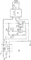
例えば、図1は、本発明の教示による顕著な特徴を示す例示的AC−DC電源装置100の機能ブロック図を示している。示されるように、全波ブリッジ整流器110が、単相AC入力電圧105を受け取るように結合される。エネルギー貯蔵回路165が、共通入力リターン160に対して正の電圧である整流電圧VRECT115を生成するために、ブリッジ整流器110から電流を受け取る。DC−DCコンバータ135が、負荷145において出力電圧VO140を生成するために、整流電圧VRECT115を受け取る。
For example, FIG. 1 shows a functional block diagram of an exemplary AC-
図示された実施例において示されるように、エネルギー貯蔵回路165は、高電圧キャパシタンスCHV120を含み、それは、高電圧キャパシタンスCHV120の両端間に整流電圧VRECT115を生成するために、整流器110から電流を受け取るように結合される。示されるように、低電圧キャパシタンスCLV125が、高電圧キャパシタンスCHV120に結合され、可変インピーダンス素子ZV155が、低電圧キャパシタンスCLV125及び高電圧キャパシタンスCHV120に結合される。
As shown in the illustrated embodiment, the
以下に、より詳細に論じられるように、駆動回路130が、整流電圧VRECT115を感知するように結合される電圧センサ134に応答して駆動信号150を生成するように結合される駆動信号発生器132を含む。駆動信号150は、整流電圧VRECT115に応答して可変インピーダンス素子ZV155を制御するように結合され、それにより、整流電圧VRECT115が第2の閾値未満である場合、可変インピーダンス素子ZV155では、低電圧キャパシタンスCLV125が整流器110からの電流を受け取ることが可能になる。整流電圧VRECT115が第1の閾値より大きい場合、可変インピーダンス素子ZV155は、低電圧キャパシタンスCLV125が整流器110から電流を受け取るのを回避するように結合される。一実施例では、第1の閾値は、第2の閾値と実質的に等しい。別の実施例では、第1の閾値は、第2の閾値より大きい。
Drive signal generation coupled to drive
例えば、図1の実施例は、エネルギー貯蔵回路165が高い定格電圧を有する小さなキャパシタンスCHV120と、実質的により低い定格電圧を有する大きなキャパシタンスCLV125とを含むことを示している。一実施例では、定格電圧CHVとCLVの比率は、2:1に等しく、又はそれより大きい。また、エネルギー貯蔵回路165は、可変インピーダンス素子ZV155を含み、そのインピーダンスは、電圧センサ134によって感知されると、整流電圧VRECT115の大きさに応答する駆動回路130の駆動信号発生器132からの駆動信号150に応答する。
For example, the embodiment of FIG. 1 shows that the
実施例では、エネルギー貯蔵回路165内の低電圧キャパシタンスCLV125の一方の端子が、整流電圧VRECT115に結合される。エネルギー貯蔵回路165における低電圧キャパシタンスCLV125の他方の端子は、可変インピーダンス素子ZV155に結合される。エネルギー貯蔵回路165における可変インピーダンス素子ZV155は、低電圧キャパシタンスCLV125と共通入力リターン160の間に結合される。そのため、低電圧キャパシタンスCLV125は、ハイサイド要素と呼ばれることがあり、それに対し、可変インピーダンス素子ZVは、ローサイド要素と呼ばれることがある。
In one embodiment, one terminal of low
一実施例では、可変インピーダンス素子ZV155は、駆動信号150に応答して非常に高いインピーダンスから非常に低いインピーダンスに変わる場合がある。実施例では、可変インピーダンス素子ZV155の非常に高いインピーダンスは、効率的に、開放スイッチである。開放スイッチは、電流を導くことが不可能なものである。可変インピーダンス素子ZV155の非常に低いインピーダンスは、効率的に、閉鎖スイッチである。閉鎖スイッチは、電流を導くことが可能なものである。また、典型的には、閉鎖スイッチは、それが電流を導いているときは、その導電端子間に低電圧を有する。一実施例では、閉鎖スイッチの導電端子間の電圧は、整流電圧VRECT115の値の10%以下である。一実施例では、また、可変インピーダンス素子ZV155は、駆動信号150の値に応答してそれほど高くもなく、それほど低くもない中間のインピーダンスの値を有する場合もある。
In one example, the variable impedance element Z V 155 may change from a very high impedance to a very low impedance in response to the
以下に、さらに詳細に論じられるように、一実施例における可変インピーダンス素子ZV155及び駆動回路130では、整流電圧VRECT115が低電圧キャパシタンスCLV125の定格電圧を超えない閾値未満であった場合だけ、低電圧キャパシタンスCLV125が整流器110からの電流を受け取ることが可能になる。したがって、整流電圧VRECT115の谷がその最小の所望の値を下回らないようにするのに小さいキャパシタンスだけを必要とするほど、単相AC入力電圧105が高い場合、エネルギー貯蔵回路165内の高定格電圧を有する小さいキャパシタンスCHV120だけが、ブリッジ整流器110からの電流を受け取ることが可能になる。整流電圧VRECT115の谷がその最小の所望の値を下回らないようにするのに大きなキャパシタンスを必要とするほど、AC入力電圧が低い場合、エネルギー貯蔵回路内の高定格電圧を有する小さいキャパシタンスCHV120と、低定格電圧を有する大きなキャパシタンスCLV125との双方がブリッジ整流器110からの電流を受け取ることが可能になる。他の実施例では、キャパシタンスCHV120及びCLV125のそれぞれは、1つ又は複数の個々のコンデンサによって達成可能であることに留意されたい。
As will be discussed in more detail below, in variable
図2は、本発明の教示による例示的電源装置200のエネルギー貯蔵回路内でキャパシタンス125を係合し、また切り離す可変インピーダンス素子155を有する実施例を示している。一実施例では、可変インピーダンス素子155は、例示的AC−DC電源装置200に示されるように、一方向だけに非常に高いインピーダンスであることが可能である。示されるように、駆動回路130の駆動信号発生器132からの駆動信号150により、可変インピーダンス素子155内のスイッチS1 255を開放、又は閉鎖することが可能である。低電圧キャパシタンスCLV125と、示されるような共通入力リターン160を通じて高電圧キャパシタンスCHV120に結合される、可変インピーダンス素子155内のダイオードD1 205では、スイッチS1 255が開放されている場合でも、電流が可変インピーダンス素子155を一方向に通過することが可能になる。図2の実施例では、低電圧キャパシタンスCLV125は、スイッチS1 255が開放、又は閉じている場合、放電することが可能であるが、スイッチS1 255が開放している場合、低電圧キャパシタンスCLV125は充電することは不可能である。
FIG. 2 illustrates an embodiment having a
図3は、本発明の教示による例示的電源装置300のエネルギー貯蔵回路内でキャパシタンス125を係合し、また切り離すように結合されるトランジスタ355及び3端子分流調整器315を含む例示的電源装置300である。一実施例では、駆動回路330の3端子分流調整器315は、TL431調整器である。駆動回路330の抵抗320は、DC−DCコンバータ135からバイアス電圧VBIAS325を一方の端部で受け取る。3端子分流調整器315は、駆動信号150の電圧を変えるために、抵抗320から電流を引き込む。
FIG. 3 illustrates an
図示された実施例において示されるように、第1の抵抗305及び第2の抵抗310を含む電圧分配器が、整流電圧VRECT115を感知し、閾値電圧を設定するように結合される。一実施例では、整流電圧VRECT115が閾値電圧より大きい場合、駆動信号150は低くなる。整流電圧VRECT115が閾値電圧未満である場合、駆動信号150は高くなる。
As shown in the illustrated embodiment, a voltage divider including a
示されている実施例では、トランジスタQ1 355が、図2の実施例において、可変インピーダンス素子155の機能を実施するために、駆動信号150を受け取るように結合される。トランジスタQ1 355は、図3に示されている例示的エネルギー貯蔵回路における金属酸化膜半導体電界効果トランジスタ(MOSFET)である。整流電圧VRECTが閾値電圧より大きい場合、トランジスタQ1 355はオフである。整流電圧VRECT115が閾値電圧未満である場合、トランジスタQ1 355はオンである。一実施例では、この状態は、整流電圧115の谷電圧が閾値電圧より下に下がることが可能になる値を単相AC供給電圧105が下回っている場合に、又は一時的な保持状態中に、存在することが可能になる。駆動信号150が失われた場合、例えば、駆動回路330に故障があり、又はVBIAS325が失われた場合、トランジスタQ1 355のゲート367とソース366の間の抵抗335は、確実にトランジスタQ1 355をオフにする。単相AC入力電圧VAC105が解除された場合、電源装置300は、短い保持時間を過ぎては、もはや動作することができなくなることを理解されたい。一実施例では、典型的な必要保持時間は、10ミリ秒である。
In the embodiment shown,
別の実施例では、ヒステリシスが、下限閾値電圧より大きな上限閾値電圧を定めるために駆動回路330内に導入される。ヒステリシスは、ノイズに対するある程度の耐性を回路に与える。ヒステリシスにより、整流電圧VRECTは、トランジスタQ1 355がオンからオフに変わるための上限閾値を上回っていなくてはならず、整流電圧VRECTは、トランジスタQ1 355がオフからオンに変わるための下限閾値電圧を下回っていなくてはならない。
In another embodiment, hysteresis is introduced into the
さらなる別の実施例では、駆動回路330は、装置のための最大定格値未満であるようにトランジスタQ1 355内の電流を制限するように結合される。一実施例では、トランジスタ内の電流を制御する技術により、トランジスタ内の電流が測定される。別の実施例では、キャパシタンスに結合されるトランジスタ内の電流を制御する技術により、トランジスタ又は可変インピーダンス素子の両端間の電圧の変化率が制限される。一実施例では、可変インピーダンス素子355の両端間の電圧の変化率を制限することは、任意選択のコンデンサ365を使用して実施可能である。可変インピーダンス素子355がオフである場合、電圧は、抵抗335の存在により、可変インピーダンス素子355の両端間の電圧に実質的に等しいコンデンサ365の両端間に現れる。可変インピーダンス素子355の両端間の電圧が、それがオンにされたときに下がると、その結果生じるコンデンサ365の両端間の電圧の変化により、抵抗320を通じて電流が引き込まれ、抵抗320の両端間で下がった電圧が上昇する。そのため、例示的MOSFET可変インピーダンス素子355のゲート端子367とソース端子366の間に現れる電圧は、コンデンサ365が使用されなかった場合よりゆっくりと上がる。そのため、コンデンサ365の効果は、可変インピーダンス素子355の両端間の電圧の変化率を制限することである。任意選択のコンデンサ365は、低電圧コンデンサCLV125の初期充電中の低電圧コンデンサCLV125を流れ、突入電流と呼ばれることの多い最大電流を制限することが望ましい実施例において使用可能になる。可変インピーダンス素子355の両端間の電圧の変化率を制限することによって、低電圧コンデンサCLV125内を流れる電流は制限される。
In yet another embodiment,
図4は、本発明の教示による例示的電源装置のエネルギー貯蔵回路における可変インピーダンス素子の対応する状態と共に、例示的電源装置における整流電圧レベルの尺度を示している。具体的には、図4の例示的図400は、トランジスタQ1 355の状態と、整流電圧VRECT115の複数の値について図3の電源装置300のバルク・キャパシタンス上のリップル電圧とを示している。整流電圧VRECTが十分なバイアス電圧VBIAS325を生成するのにDC−DCコンバータ135についてゼロボルトと最小値425の間である場合、トランジスタQ1 355はオフである。整流電圧VRECT115が最小値425と閾値435の間である場合、トランジスタQ1 355はオンである。実施例では、閾値435は、低電圧キャパシタンスCLV125の定格電圧410よりわずかに低くなるように設定されている。整流電圧VRECT115が閾値電圧435より大きい場合、トランジスタQ1 355はオフである。高電圧キャパシタンスCHV120の定格電圧は、最大期待単相AC入力電圧VAC105で、整流電圧VRECT115の値405より大きくなるように選択される。
FIG. 4 shows a measure of the rectified voltage level in an exemplary power supply, along with corresponding states of variable impedance elements in the energy storage circuit of the exemplary power supply in accordance with the teachings of the present invention. Specifically, the exemplary diagram 400 of FIG. 4 shows the state of the
また、図4は、トランジスタQ1 335が、それぞれオフ及びオンである場合の典型的なリップル電圧430及び440を示している。一実施例450では、トランジスタQ1 355がリップル電圧の周波数においてオン及びオフになるように、単相AC入力電圧115が典型的な値である場合、整流電圧VRECT115のピークは閾値435を上回り、整流電圧VRECT115の谷は閾値435を下回る。
FIG. 4 also shows
一実施例では、高電圧キャパシタンスCHV120の値は、高AC入力電圧でDC−DCコンバータ135の最小限の要件を満たすように選択される。低電圧キャパシタンスCLV125の値は、DC−DCコンバータ135のすべての特定の動作条件の下で、所要の出力電圧VO140を生成するために、整流電圧VRECT115の谷をDC−DCコンバータ135についての最小値420を上回った状態に保つように選択される。エネルギー貯蔵回路におけるキャパシタンスは、整流電圧VRECT115が値415である場合、保持時間を維持するのに十分なエネルギーを含んでいなくてはならない。値415は、電源装置が動作するために特定される最小単相AC入力電圧105で谷電圧に対応する。
In one embodiment, the value of the high
図5は、エネルギー貯蔵回路のための可変インピーダンス素子555と、DC−DCコンバータのための可変インピーダンス素子515と、集積回路505に含まれる電源装置コントローラ回路510とを有する例示的AC−DC電源装置500を示している。実施例では、電源装置コントローラ回路510は、駆動回路530と、DC−DCコンバータ制御回路532とを備える。一実施例では、駆動回路530は、機能において、駆動回路130及び330と類似しており、類似した特徴を含むことが可能である。示されるように、トランジスタQ1 555は、駆動回路530からの駆動信号550に応答してエネルギー貯蔵回路の低電圧キャパシタンスCLV125を係合し、また切り離す可変インピーダンス素子である。一実施例では、DC−DCコンバータ制御回路532は、電源装置の出力において負荷145にエネルギーの転送を制御するために、フィードバック信号531に応答してトランジスタQ2 515を切り替えるように結合される。トランジスタQ2 515は、図示の実施例ではフライバック・コンバータとして示されているDC−DCコンバータの変圧器520の第1の巻き線を、DC−DCコンバータ制御回路532からの駆動信号525に応答して切り替える可変インピーダンス素子である。ダイオード545とコンデンサ540が、出力電圧VO140を負荷145に送るために変圧器520の第2の巻き線に結合される。
FIG. 5 illustrates an exemplary AC-DC power supply having a
図示の実施例において示されるように、電源装置コントローラ回路510は、整流電圧VRECT115からの入力電圧信号535と、変圧器520の第3の巻き線からのフィードバック信号531とを受け取る。電源装置コントローラ回路510は、エネルギー貯蔵回路の低電圧キャパシタンスCLV125を係合し、また切り離すために、トランジスタQ1 555に第1の駆動信号550を供給する。また、電源装置コントローラ回路510は、フィードバック信号531に応答して出力電圧VO140を調整するために、トランジスタQ2 515をオン及びオフに切り替える第2の駆動信号525を供給する。別の実施例では、フィードバック信号531は、変圧器520の巻き線からではなく、オプトカプラから受け取られる。一実施例では、入力電圧信号535は、電源装置コントローラ回路510内で、駆動回路530とDC−DCコンバータ制御回路532に結合される。一実施例では、駆動回路530と結合した入力電圧信号535は、機能において、図1及び2の素子134と類似した駆動回路530の内部の電圧センサ回路に信号を供給する。一実施例では、DC−DCコンバータ制御回路532と結合した入力電圧信号535は、入力電圧105が上昇すると、例えば、Q2 515を流れる最大電流を抑えるために使用可能であるフィード・フォワード信号を供給する。一実施例では、フィードバック信号531は、電源装置コントローラ回路510内で、駆動回路530とDC−DCコンバータ制御回路532に結合される。一実施例では、駆動回路530に結合したフィードバック信号531では、フィードバック信号531が失われた場合に生じる故障状態の場合、駆動信号550が低く保たれることが可能になる。図示の実施例では、駆動回路530とDC−DCコンバータ制御回路532の間のこれらの内部接続及び複数の他の接続は、本発明の教示をわかりにくくしないようにするために図示されていない。
As shown in the illustrated embodiment, the power
図6は、本発明の教示による例示的AC−DC電源装置内のエネルギー貯蔵の例示的方法のための流れ図600である。示されるようにブロック610で開始した後、整流単相AC電圧は、ブロック620でDC−DCコンバータへの入力において感知される。整流電圧は、ブロック630で閾値と比較される。整流電圧が閾値未満であった場合、ブロック640で低電圧キャパシタンスは、電流を受け取るためにエネルギー貯蔵回路内で係合される。整流電圧が閾値以上であった場合、ブロック650でエネルギー貯蔵回路内の低電圧キャパシタンスは、受け取った電流から切り離される。DC−DCコンバータへの入力において整流電圧を感知することは、ブロック620で継続する。
FIG. 6 is a flow diagram 600 for an exemplary method of energy storage in an exemplary AC-DC power supply according to the teachings of the present invention. After starting at
図示されている実施例では、全波ブリッジ整流回路110が使用されているが、本発明の教示からの恩恵をさらに受けつつも、半波整流回路が利用可能であることを理解されたい。さらには、本発明の恩恵は、エネルギー貯蔵回路165にいずれの誘導性回路素子も必要とすることなく、得られることも理解されたい。
In the illustrated embodiment, a full wave
要約書内に記載されていることをも含む本発明の図示されている実施例の上述の説明は、開示される精密な形態に包括的又は限定的であるように意図されない。本発明の特定の実施形態又は本発明のための実施例が本明細書において例示目的として記載されているが、様々な均等の修正形態が、本発明の広範な精神及び範囲から逸脱することなく可能である。実際に、特定の電圧、電流、周波数、出力領域値、時間などが、説明目的として提供され、他の値もまた本発明の教示による他の実施形態及び実施例において使用可能であることを理解されたい。 The above description of illustrated embodiments of the invention, including what is described in the abstract, is not intended to be exhaustive or limiting to the precise form disclosed. While specific embodiments of the invention or examples for the invention have been described herein for purposes of illustration, various equivalent modifications may be made without departing from the broad spirit and scope of the invention. Is possible. Indeed, specific voltages, currents, frequencies, output region values, times, etc. are provided for illustrative purposes, and it is understood that other values can also be used in other embodiments and examples in accordance with the teachings of the present invention. I want to be.
これらの修正形態は、上述の詳細な説明に照らして、本発明の実施例に対して行われることが可能である。添付の特許請求の範囲に使用される用語は、明細書及び特許請求の範囲内に開示される特定の実施形態に本発明を限定すると解釈されるべきではない。そうではなく、範囲は、特許請求の範囲の解釈の確立された原則により解釈されるべきである添付の特許請求の範囲によって全体的に決定されるべきである。したがって、本明細書及び図面は、制限的ではなく例示的であるとみなされるべきである。 These modifications can be made to embodiments of the invention in light of the above detailed description. The terms used in the following claims should not be construed to limit the invention to the specific embodiments disclosed in the specification and the claims. Instead, the scope should be determined entirely by the appended claims, which are to be construed in accordance with established principles of claim interpretation. Accordingly, the specification and drawings are to be regarded as illustrative rather than restrictive.
100 AC−DC電源装置
105 単相AC入力電圧
110 全波ブリッジ整流器
115 整流電圧
120 高電圧キャパシタンス
125 低電圧キャパシタンス
130 駆動回路
132 駆動信号発生器
134 電圧センサ
135 DC−DCコンバータ
140 出力電圧
145 負荷
150 駆動信号
155 可変インピーダンス素子
160 共通入力リターン
165 エネルギー貯蔵回路
200 電源装置
205 ダイオード
255 スイッチ
300 電源装置
305 第1の抵抗
310 第2の抵抗
315 3端子分流調整器
320 抵抗
325 バイアス電圧
330 駆動回路
335 抵抗
355 可変インピーダンス素子、トランジスタ
365 コンデンサ
366 ソース
367 ゲート
405 値
410 定格電圧
415 値
420 最小値
425 最小値
430 リップル電圧
435 閾値
440 リップル電圧
450 実施例
500 AC−DC電源装置
505 集積回路
510 電源装置コントローラ回路
515 可変インピーダンス素子、トランジスタ
520 変圧器
525 駆動信号
530 駆動回路
531 フィードバック信号
532 DC−DCコンバータ制御回路
535 入力電圧信号
540 コンデンサ
545 ダイオード
550 駆動信号
555 可変インピーダンス素子、トランジスタ
600 流れ図
DESCRIPTION OF
Claims (25)
低電圧キャパシタンスと高電圧キャパシタンスに結合される可変インピーダンス素子に結合される駆動信号を生成するための駆動信号発生器と、
前記駆動信号発生器に結合され、前記高電圧キャパシタンスの両端間の電圧を感知するように結合される電圧センサであって、前記駆動回路は、前記電圧センサに応答して前記可変インピーダンス素子を制御するように結合され、それにより、前記低電圧キャパシタンスは、前記高電圧キャパシタンスの両端間の前記電圧が第2の閾値未満である場合、前記電源装置の前記入力からの電流を受け取ることが可能になり、前記低電圧キャパシタンスは、前記高電圧キャパシタンスの両端間の前記電圧が第1の閾値より大きい場合、前記電源装置の前記入力からの電流を受け取るのが回避される、電圧センサと、
を備える駆動回路。 A drive circuit for use in the power supply having a rectifier coupled to generate a rectified voltage in response to a single phase AC voltage at the input of the power supply,
A drive signal generator for generating a drive signal coupled to a variable impedance element coupled to the low voltage capacitance and the high voltage capacitance;
A voltage sensor coupled to the drive signal generator and coupled to sense a voltage across the high voltage capacitance, the drive circuit controlling the variable impedance element in response to the voltage sensor. Coupled so that the low voltage capacitance can receive current from the input of the power supply if the voltage across the high voltage capacitance is less than a second threshold. The low voltage capacitance is a voltage sensor that is prevented from receiving current from the input of the power supply if the voltage across the high voltage capacitance is greater than a first threshold;
A drive circuit comprising:
前記電源装置のDC−DCコンバータへの入力において電圧を感知するステップと、
前記感知された電圧が第2の閾値未満である場合、前記電源装置の入力に結合される低電圧キャパシタンスを係合するステップと、
前記感知された電圧が第1の閾値より大きい場合、前記低電圧キャパシタンスを切り離すステップと、
を含む方法。 A method of controlling a power supply device that operates from a rectified single-phase AC input voltage,
Sensing a voltage at an input to a DC-DC converter of the power supply;
Engaging a low voltage capacitance coupled to an input of the power supply if the sensed voltage is less than a second threshold;
Detaching the low voltage capacitance if the sensed voltage is greater than a first threshold;
Including methods.
前記整流器に結合され、高電圧キャパシタンス、低電圧キャパシタンス、及び可変インピーダンス素子を含むエネルギー貯蔵回路であって、前記整流器から受け取られた電流は、前記高電圧キャパシタンスの両端間に電圧を生成するように結合され、前記低電圧キャパシタンスは、前記高電圧キャパシタンスに結合され、前記可変インピーダンス素子は、前記低電圧キャパシタンス及び前記高電圧キャパシタンスに結合される、エネルギー貯蔵回路と、
前記高電圧キャパシタンスの両端間の前記電圧に応答して駆動信号を生成するように結合される駆動回路であって、前記駆動信号は、前記高電圧キャパシタンスの両端間の前記電圧が第1の閾値電圧より大きい場合、前記低電圧キャパシタンスが前記整流器からの電流を受け取るのを防ぐために、及び前記高電圧キャパシタンスの両端間の前記電圧が第2の閾値電圧未満である場合、前記低電圧キャパシタンスが前記整流器からの電流を受け取ることを可能にするために、前記可変インピーダンス素子によって受け取られるように結合される、駆動回路と、
を備える電源装置。 A rectifier coupled to receive a single phase AC input voltage;
An energy storage circuit coupled to the rectifier and including a high voltage capacitance, a low voltage capacitance, and a variable impedance element, such that a current received from the rectifier generates a voltage across the high voltage capacitance. An energy storage circuit coupled, wherein the low voltage capacitance is coupled to the high voltage capacitance, and the variable impedance element is coupled to the low voltage capacitance and the high voltage capacitance;
A drive circuit coupled to generate a drive signal in response to the voltage across the high voltage capacitance, wherein the drive signal is such that the voltage across the high voltage capacitance is a first threshold value. If greater than a voltage, the low voltage capacitance is less than a second threshold voltage to prevent the low voltage capacitance from receiving current from the rectifier and if the voltage across the high voltage capacitance is less than a second threshold voltage A drive circuit coupled to be received by the variable impedance element to enable receiving current from the rectifier;
A power supply device comprising:
前記電源装置の出力へのエネルギーの転送を制御するために、第1の可変インピーダンス素子を切り替えるように結合されるDC−DCコンバータ・コントローラ回路と、
低電圧キャパシタンスと高電圧キャパシタンスに結合される第2の可変インピーダンス素子に結合される駆動信号を生成するための駆動信号発生器、及び
前記駆動信号発生器に結合され、前記高電圧キャパシタンスの両端間の電圧を感知するように結合される電圧センサであって、前記駆動回路は、前記電圧センサに応答して前記第2の可変インピーダンス素子を制御するように結合され、それにより、前記低電圧キャパシタンスは、前記高電圧キャパシタンスの両端間の前記電圧が第2の閾値未満である場合、前記電源装置の前記入力からの電流を受け取ることが可能になり、前記低電圧キャパシタンスは、前記高電圧キャパシタンスの両端間の前記電圧が第1の閾値より大きい場合、前記電源装置の前記入力からの電流を受け取るのが回避される、電圧センサを
含む駆動回路と、
を備える電源装置コントローラ回路。 A power supply controller circuit for use in said power supply having a rectifier coupled to generate a rectified voltage in response to a single phase AC voltage at an input of the power supply, comprising:
A DC-DC converter controller circuit coupled to switch a first variable impedance element to control transfer of energy to the output of the power supply;
A drive signal generator for generating a drive signal coupled to a second variable impedance element coupled to the low voltage capacitance and the high voltage capacitance; and between the ends of the high voltage capacitance coupled to the drive signal generator Wherein the drive circuit is coupled to control the second variable impedance element in response to the voltage sensor, thereby the low voltage capacitance. Is able to receive current from the input of the power supply if the voltage across the high voltage capacitance is less than a second threshold, and the low voltage capacitance is a value of the high voltage capacitance. If the voltage across is greater than a first threshold, it is not possible to receive current from the input of the power supply. A drive circuit including a voltage sensor to be avoided;
A power supply controller circuit comprising:
Applications Claiming Priority (2)
| Application Number | Priority Date | Filing Date | Title |
|---|---|---|---|
| US11/873,697 US7760524B2 (en) | 2007-10-17 | 2007-10-17 | Method and apparatus to reduce the volume required for bulk capacitance in a power supply |
| US11/873,697 | 2007-10-17 |
Publications (3)
| Publication Number | Publication Date |
|---|---|
| JP2009100647A true JP2009100647A (en) | 2009-05-07 |
| JP2009100647A5 JP2009100647A5 (en) | 2011-11-17 |
| JP5579378B2 JP5579378B2 (en) | 2014-08-27 |
Family
ID=40448411
Family Applications (1)
| Application Number | Title | Priority Date | Filing Date |
|---|---|---|---|
| JP2008260444A Active JP5579378B2 (en) | 2007-10-17 | 2008-10-07 | Method and apparatus for reducing the capacitance required for bulk capacitance in a power supply |
Country Status (4)
| Country | Link |
|---|---|
| US (1) | US7760524B2 (en) |
| EP (1) | EP2058933A3 (en) |
| JP (1) | JP5579378B2 (en) |
| CN (1) | CN101414764B (en) |
Cited By (1)
| Publication number | Priority date | Publication date | Assignee | Title |
|---|---|---|---|---|
| JP2011061928A (en) * | 2009-09-08 | 2011-03-24 | Hitachi Automotive Systems Ltd | Vehicular alternator, and rectifier of vehicular alternator |
Families Citing this family (26)
| Publication number | Priority date | Publication date | Assignee | Title |
|---|---|---|---|---|
| JP5089536B2 (en) * | 2008-09-10 | 2012-12-05 | 株式会社リコー | CURRENT LIMIT CIRCUIT AND CURRENT LIMIT CIRCUIT DRIVING METHOD |
| US8063622B2 (en) | 2009-10-02 | 2011-11-22 | Power Integrations, Inc. | Method and apparatus for implementing slew rate control using bypass capacitor |
| US8634218B2 (en) | 2009-10-06 | 2014-01-21 | Power Integrations, Inc. | Monolithic AC/DC converter for generating DC supply voltage |
| US8369111B2 (en) | 2010-08-02 | 2013-02-05 | Power Integrations, Inc. | Ultra low standby consumption in a high power power converter |
| CN102543008B (en) * | 2010-12-20 | 2013-11-06 | 晨星软件研发(深圳)有限公司 | Voltage-stabilizing protection circuit and display controller to which voltage-stabilizing protection circuit belongs, as well as driving method of light-emitting diode |
| US9455621B2 (en) | 2013-08-28 | 2016-09-27 | Power Integrations, Inc. | Controller IC with zero-crossing detector and capacitor discharge switching element |
| RU2689304C2 (en) * | 2014-01-13 | 2019-05-27 | Филипс Лайтинг Холдинг Б.В. | Buffering capacitor for rectifier with diode bridge with controlled discharge current |
| CN105763078B (en) * | 2014-12-18 | 2019-07-05 | 台达电子工业股份有限公司 | Switching Power Supply and bus capacitor voltage control method for Switching Power Supply |
| US9667154B2 (en) * | 2015-09-18 | 2017-05-30 | Power Integrations, Inc. | Demand-controlled, low standby power linear shunt regulator |
| CN108604858A (en) * | 2015-10-23 | 2018-09-28 | 香港大学 | Plug and play ripple for the DC voltage link in power electronic system and DC power grids calms down device |
| US9602009B1 (en) | 2015-12-08 | 2017-03-21 | Power Integrations, Inc. | Low voltage, closed loop controlled energy storage circuit |
| US9629218B1 (en) | 2015-12-28 | 2017-04-18 | Power Integrations, Inc. | Thermal protection for LED bleeder in fault condition |
| US9977455B2 (en) | 2016-04-11 | 2018-05-22 | Futurewei Technologies, Inc. | Method and apparatus for filtering a rectified voltage |
| US9923451B2 (en) * | 2016-04-11 | 2018-03-20 | Futurewei Technologies, Inc. | Method and apparatus for filtering a rectified voltage signal |
| US10033264B2 (en) * | 2016-04-29 | 2018-07-24 | Infineon Technologies Austria Ag | Bulk capacitor switching for power converters |
| US10033269B2 (en) | 2016-04-29 | 2018-07-24 | Infineon Technologies Austria Ag | Voltage doubler with capacitor module for increasing capacitance |
| CN106505886A (en) * | 2016-11-11 | 2017-03-15 | 安徽维德工业自动化有限公司 | The image output module electric power system of the full light multimedia platform of high definition |
| CN107295717A (en) * | 2017-06-29 | 2017-10-24 | 赛尔富电子有限公司 | A kind of control circuit for LED lamp |
| US10224806B1 (en) | 2017-11-16 | 2019-03-05 | Infineon Technologies Austria Ag | Power converter with selective transformer winding input |
| US10432097B2 (en) * | 2017-11-30 | 2019-10-01 | Infineon Technologies Austria Ag | Selection control for transformer winding input in a power converter |
| US11509219B2 (en) | 2019-11-15 | 2022-11-22 | Power Integrations, Inc | Reservoir capacitor for boost converters |
| US11431261B2 (en) | 2019-12-11 | 2022-08-30 | Gan Systems Inc. | Hybrid bulk capacitance circuit for AC input AC/DC switching mode power supplies |
| US11374489B2 (en) | 2019-12-11 | 2022-06-28 | Gan Systems Inc. | Hybrid bulk capacitance circuit for AC/DC charger |
| CN113394989B (en) * | 2020-03-12 | 2023-08-08 | Oppo广东移动通信有限公司 | Power conversion device and charging control method |
| GB2606230B (en) * | 2021-04-30 | 2023-12-27 | Dyson Technology Ltd | Haircare appliance |
| EP4186733A1 (en) | 2021-11-24 | 2023-05-31 | Power Integrations, Inc. | Active discharge of an electric drive system |
Citations (4)
| Publication number | Priority date | Publication date | Assignee | Title |
|---|---|---|---|---|
| JPS6091868A (en) * | 1983-10-24 | 1985-05-23 | Trio Kenwood Corp | Power source circuit |
| JPS60109761A (en) * | 1983-10-25 | 1985-06-15 | ベー・ベー・ツエー・アクチエンゲゼルシヤフト・ブラウン・ボベリ・ウント・コンパニー | Ac filter circuit device |
| JPH08280178A (en) * | 1995-04-07 | 1996-10-22 | Philips Electron Nv | Circuit device for generating separated output voltage |
| JP2005006398A (en) * | 2003-06-11 | 2005-01-06 | Flying Mole Corp | Ac/dc converter |
Family Cites Families (17)
| Publication number | Priority date | Publication date | Assignee | Title |
|---|---|---|---|---|
| US5394017A (en) | 1991-11-05 | 1995-02-28 | Alliedsignal Inc. | Circuit for sustaining output power during input power interruption |
| US5561596A (en) | 1994-02-22 | 1996-10-01 | International Business Machines Corporation | AC line stabilization circuitry for high power factor loads |
| FR2734102B1 (en) * | 1995-05-09 | 1997-07-25 | Sgs Thomson Microelectronics | IMPROVING THE POWER FACTOR OF A RECTIFIED FEED |
| US5825639A (en) * | 1997-10-16 | 1998-10-20 | Magnetek, Inc. | DC bus capacitor arrangement |
| US5999429A (en) | 1997-12-19 | 1999-12-07 | Dell Usa, L.P. | Bulk filter capacitor discharge in a switching power supply |
| US6043705A (en) | 1998-03-25 | 2000-03-28 | Lucent Technologies Inc. | Boost converter having extended holdup time and method of operation |
| KR100355037B1 (en) * | 1999-11-02 | 2002-10-05 | 삼성전자 주식회사 | World Wide Power Supply Apparatus |
| US6504497B2 (en) | 2000-10-30 | 2003-01-07 | Delta Electronics, Inc. | Hold-up-time extension circuits |
| US6738277B2 (en) | 2001-11-27 | 2004-05-18 | Power Integrations, Inc. | Method and apparatus for balancing active capacitor leakage current |
| US6538906B1 (en) | 2002-02-11 | 2003-03-25 | Delta Electronics, Inc. | Energy storage circuit for DC-DC converter |
| US6788040B2 (en) | 2002-09-26 | 2004-09-07 | Eni Technology, Inc. | Power holdup circuit with increased power factor |
| US6879140B2 (en) | 2002-09-26 | 2005-04-12 | Mks Instruments, Inc. | Power holdup circuit |
| US6882212B2 (en) | 2003-05-16 | 2005-04-19 | Power Integrations, Inc. | Method and apparatus for extending the size of a transistor beyond one integrated circuit |
| US7061212B2 (en) | 2003-08-08 | 2006-06-13 | Astec International Limited | Circuit for maintaining hold-up time while reducing bulk capacitor size and improving efficiency in a power supply |
| US7061301B2 (en) | 2003-12-19 | 2006-06-13 | Power Integrations, Inc. | Method and apparatus switching a semiconductor switch with a multi-state drive circuit |
| WO2007003544A2 (en) * | 2005-06-30 | 2007-01-11 | Siemens Aktiengesellschaft | Frequency converter provided with a capacitorless intermediate voltage circuit |
| US7535691B2 (en) | 2006-03-30 | 2009-05-19 | Power Integrations, Inc. | Method and apparatus for an in-rush current limiting circuit |
-
2007
- 2007-10-17 US US11/873,697 patent/US7760524B2/en active Active
-
2008
- 2008-10-07 JP JP2008260444A patent/JP5579378B2/en active Active
- 2008-10-17 EP EP08166975.6A patent/EP2058933A3/en not_active Withdrawn
- 2008-10-17 CN CN200810170511.2A patent/CN101414764B/en active Active
Patent Citations (4)
| Publication number | Priority date | Publication date | Assignee | Title |
|---|---|---|---|---|
| JPS6091868A (en) * | 1983-10-24 | 1985-05-23 | Trio Kenwood Corp | Power source circuit |
| JPS60109761A (en) * | 1983-10-25 | 1985-06-15 | ベー・ベー・ツエー・アクチエンゲゼルシヤフト・ブラウン・ボベリ・ウント・コンパニー | Ac filter circuit device |
| JPH08280178A (en) * | 1995-04-07 | 1996-10-22 | Philips Electron Nv | Circuit device for generating separated output voltage |
| JP2005006398A (en) * | 2003-06-11 | 2005-01-06 | Flying Mole Corp | Ac/dc converter |
Cited By (1)
| Publication number | Priority date | Publication date | Assignee | Title |
|---|---|---|---|---|
| JP2011061928A (en) * | 2009-09-08 | 2011-03-24 | Hitachi Automotive Systems Ltd | Vehicular alternator, and rectifier of vehicular alternator |
Also Published As
| Publication number | Publication date |
|---|---|
| US20090103337A1 (en) | 2009-04-23 |
| JP5579378B2 (en) | 2014-08-27 |
| EP2058933A2 (en) | 2009-05-13 |
| CN101414764A (en) | 2009-04-22 |
| US7760524B2 (en) | 2010-07-20 |
| EP2058933A3 (en) | 2017-01-25 |
| CN101414764B (en) | 2014-07-09 |
Similar Documents
| Publication | Publication Date | Title |
|---|---|---|
| JP5579378B2 (en) | Method and apparatus for reducing the capacitance required for bulk capacitance in a power supply | |
| US10608525B2 (en) | Method and apparatus for implementing a power converter input terminal voltage discharge circuit | |
| US10903752B2 (en) | AC-DC converter with secondary side-control and synchronous rectifier sense architecture | |
| US10910954B1 (en) | Power saving technique in detach condition for USB-power delivery with integrated synchronous recitifier controller | |
| US11139743B2 (en) | Accurate feed-forward sensing in flyback-transformer based secondary controller | |
| CN101572487B (en) | Semiconductor device for controlling switching power supply | |
| US9780594B2 (en) | Discharge circuit and power supply device therewith | |
| KR101365100B1 (en) | Low power consumption start-up circuit with dynamic switching | |
| EP1605576A1 (en) | Device and method for extending the input voltage range of a DC/DC converter | |
| KR20020079861A (en) | Start-up circuit for flyback converter having secondary pulse width modulation control | |
| CN103887984A (en) | Isolating converter and switching power supply comprising same | |
| TW201414155A (en) | Off-line power converter and integrated circuit suitable for use in same | |
| US9219420B1 (en) | Overvoltage protection using a tapFET | |
| US9627991B2 (en) | Rectifier with indicator switch | |
| TWI489758B (en) | Power controller, power supply and control method capable of brownin and brownout detection | |
| US20230223858A1 (en) | Secondary Side Controlled QR Flyback Converter using a Programmable Valley Algorithm | |
| TWI419450B (en) | A system and method for reducing the standby power consumption of a switch mode power converter | |
| CN113726175A (en) | Conversion device, controller and power supply control method thereof | |
| TW202406292A (en) | Power supply circuit with sufficient hold time in high-frequency varying load condition | |
| CN116260319A (en) | Power converter and power switch controller for power converter |
Legal Events
| Date | Code | Title | Description |
|---|---|---|---|
| A521 | Request for written amendment filed |
Free format text: JAPANESE INTERMEDIATE CODE: A523 Effective date: 20111003 |
|
| A621 | Written request for application examination |
Free format text: JAPANESE INTERMEDIATE CODE: A621 Effective date: 20111003 |
|
| A131 | Notification of reasons for refusal |
Free format text: JAPANESE INTERMEDIATE CODE: A131 Effective date: 20130521 |
|
| A521 | Request for written amendment filed |
Free format text: JAPANESE INTERMEDIATE CODE: A523 Effective date: 20130820 |
|
| A131 | Notification of reasons for refusal |
Free format text: JAPANESE INTERMEDIATE CODE: A131 Effective date: 20140328 |
|
| A521 | Request for written amendment filed |
Free format text: JAPANESE INTERMEDIATE CODE: A523 Effective date: 20140610 |
|
| TRDD | Decision of grant or rejection written | ||
| A01 | Written decision to grant a patent or to grant a registration (utility model) |
Free format text: JAPANESE INTERMEDIATE CODE: A01 Effective date: 20140701 |
|
| A61 | First payment of annual fees (during grant procedure) |
Free format text: JAPANESE INTERMEDIATE CODE: A61 Effective date: 20140709 |
|
| R150 | Certificate of patent or registration of utility model |
Ref document number: 5579378 Country of ref document: JP Free format text: JAPANESE INTERMEDIATE CODE: R150 |
|
| R250 | Receipt of annual fees |
Free format text: JAPANESE INTERMEDIATE CODE: R250 |
|
| R250 | Receipt of annual fees |
Free format text: JAPANESE INTERMEDIATE CODE: R250 |
|
| R250 | Receipt of annual fees |
Free format text: JAPANESE INTERMEDIATE CODE: R250 |
|
| R250 | Receipt of annual fees |
Free format text: JAPANESE INTERMEDIATE CODE: R250 |
|
| R250 | Receipt of annual fees |
Free format text: JAPANESE INTERMEDIATE CODE: R250 |
|
| R250 | Receipt of annual fees |
Free format text: JAPANESE INTERMEDIATE CODE: R250 |
|
| R250 | Receipt of annual fees |
Free format text: JAPANESE INTERMEDIATE CODE: R250 |