JP2009099384A - Image display device - Google Patents
Image display device Download PDFInfo
- Publication number
- JP2009099384A JP2009099384A JP2007270027A JP2007270027A JP2009099384A JP 2009099384 A JP2009099384 A JP 2009099384A JP 2007270027 A JP2007270027 A JP 2007270027A JP 2007270027 A JP2007270027 A JP 2007270027A JP 2009099384 A JP2009099384 A JP 2009099384A
- Authority
- JP
- Japan
- Prior art keywords
- electrode
- electron
- image display
- phosphor
- electron emission
- Prior art date
- Legal status (The legal status is an assumption and is not a legal conclusion. Google has not performed a legal analysis and makes no representation as to the accuracy of the status listed.)
- Pending
Links
Images


Classifications
-
- H—ELECTRICITY
- H01—ELECTRIC ELEMENTS
- H01J—ELECTRIC DISCHARGE TUBES OR DISCHARGE LAMPS
- H01J31/00—Cathode ray tubes; Electron beam tubes
- H01J31/08—Cathode ray tubes; Electron beam tubes having a screen on or from which an image or pattern is formed, picked up, converted, or stored
- H01J31/10—Image or pattern display tubes, i.e. having electrical input and optical output; Flying-spot tubes for scanning purposes
- H01J31/12—Image or pattern display tubes, i.e. having electrical input and optical output; Flying-spot tubes for scanning purposes with luminescent screen
- H01J31/123—Flat display tubes
- H01J31/125—Flat display tubes provided with control means permitting the electron beam to reach selected parts of the screen, e.g. digital selection
- H01J31/127—Flat display tubes provided with control means permitting the electron beam to reach selected parts of the screen, e.g. digital selection using large area or array sources, i.e. essentially a source for each pixel group
-
- H—ELECTRICITY
- H01—ELECTRIC ELEMENTS
- H01J—ELECTRIC DISCHARGE TUBES OR DISCHARGE LAMPS
- H01J29/00—Details of cathode-ray tubes or of electron-beam tubes of the types covered by group H01J31/00
- H01J29/02—Electrodes; Screens; Mounting, supporting, spacing or insulating thereof
- H01J29/04—Cathodes
-
- H—ELECTRICITY
- H01—ELECTRIC ELEMENTS
- H01J—ELECTRIC DISCHARGE TUBES OR DISCHARGE LAMPS
- H01J2329/00—Electron emission display panels, e.g. field emission display panels
- H01J2329/02—Electrodes other than control electrodes
- H01J2329/04—Cathode electrodes
- H01J2329/0486—Cold cathodes having an electric field parallel to the surface thereof, e.g. thin film cathodes
Landscapes
- Cathode-Ray Tubes And Fluorescent Screens For Display (AREA)
Abstract
Description
本発明は、マトリクス状に配置した電子放出素子と蛍光体とを用いて画像を表示する画像表示装置に関する。 The present invention relates to an image display device that displays an image using electron-emitting devices and phosphors arranged in a matrix.
マトリクス電子源ディスプレイとも称する画像表示装置は、互いに直交する電極群の交点を画素とし、各画素に電子放出素子を設け、各電子放出素子への印加電圧またはパルス幅を調整することによって放出電子量を調整し、その放出電子を真空中で加速した後、蛍光体に照射し、照射した部分の蛍光体を発光させるものである。電子放出素子として、電界放射型陰極を用いるもの、MIM(Metal‐Insulator‐Metal)型電子源を用いるもの、カーボンナノチューブ陰極を用いるもの、ダイヤモンド陰極を用いるもの、表面伝導電子放出素子を用いるもの、弾道型面電子源を用いるもの、などがある。このように、マトリクス電子源ディスプレイとは、電子放出素子と蛍光体とを組み合わせた電子線励起型平面ディスプレイを指す。 An image display device, also called a matrix electron source display, uses an intersection of electrode groups orthogonal to each other as a pixel, an electron-emitting device is provided in each pixel, and the amount of emitted electrons is adjusted by adjusting the applied voltage or pulse width to each electron-emitting device. Then, the emitted electrons are accelerated in vacuum, and then irradiated on the phosphor, so that the irradiated portion of the phosphor emits light. As an electron-emitting device, a device using a field emission cathode, a device using a MIM (Metal-Insulator-Metal) electron source, a device using a carbon nanotube cathode, a device using a diamond cathode, a device using a surface conduction electron-emitting device, Some use a ballistic surface electron source. As described above, the matrix electron source display refers to an electron beam excitation type flat display in which an electron-emitting device and a phosphor are combined.
図1は、マトリクス電子源ディスプレイの断面を示す模式図である。図1に示すように,マトリクス電子源ディスプレイでは、電子放出素子を配置した陰極板601と蛍光体を形成した蛍光板602とを対向配置した構成である。電子放出素子301から放出した電子が蛍光板に到達し蛍光体を励起して発光させるために、陰極板と蛍光板と枠部材603とで囲まれた空間を真空に保つ。外部からの大気圧に耐えるために陰極板と蛍光板との間にスペーサ(支柱)60を挿入する。
FIG. 1 is a schematic diagram showing a cross section of a matrix electron source display. As shown in FIG. 1, the matrix electron source display has a configuration in which a
蛍光板602は加速電極122を有し、加速電極122には3KV〜12KV程度の高電圧を印加する。電子放出素子301から放出された電子はこの高電圧で加速されたのち蛍光体に照射し、蛍光体を励起発光させる。
The
マトリクス電子源ディスプレイに用いる電子放出素子として薄膜電子源がある。薄膜電子源とは、上部電極、電子加速層、下部電極を積層した構造を有するもので、MIM(Metal‐Insulator‐Metal)型電子源、MOS(Metal‐Oxide‐Semiconductor)型電子源、弾道型面電子源、HEED(High‐Efficiency Electron Emission Device)型電子源などが含まれる。MIM型電子源の構造は、例えば,「特許文献1」に記載されている。MOS型電子源は、電子加速層に半導体−絶縁体積層膜を用いたもので、例えば「非特許文献1」に記載されている。弾道型面電子源は、電子加速層にポーラスシリコンなどを用いたもので、例えば「非特許文献2」に記載されている。薄膜電子源は、電子加速層中で加速した電子を真空中に放出させる。また、MIM型電子源は上部電極と下部電極に金属を用い、電子加速層に絶縁体を用いたものであり、例えば「非特許文献3」に記載されている。HEED型電子源は電子加速層にシリコン(Si)とSiO2の積層膜を用いたもので、例えば「非特許文献5」に記載されている。
There is a thin film electron source as an electron-emitting device used in a matrix electron source display. The thin-film electron source has a structure in which an upper electrode, an electron acceleration layer, and a lower electrode are stacked. The MIM (Metal-Insulator-Metal) type electron source, MOS (Metal-Oxide-Semiconductor) type electron source, ballistic type Surface electron sources, HEED (High-Efficiency Electron Emission Device) type electron sources, and the like are included. The structure of the MIM type electron source is described in, for example, “
図2は、薄膜電子源の動作原理を示すエネルギーバンド図である。下部電極13、電子加速層12、上部電極11が積層されており、上部電極11に正の電圧を印加した時の状態を図示した。MIM型電子源の場合、電子加速層12として絶縁体を用いる。上部電極−下部電極間に印加された電圧によって電子加速層12内に電界が生じる。この電界によって下部電極13中から電子がトンネル現象によって電子加速層12中に流れ込む。この電子は電子加速層12中の電界によって加速されホットエレクトロンとなる。このホットエレクトロンが上部電極11中を通過する際,一部の電子は非弾性散乱などによりエネルギーを失う。上部電極11−真空界面(すなわち、上部電極11の表面)に達した時点で、表面の仕事関数Φよりも大きな運動エネルギーを有する電子は上部電極11の表面から真空中10に放出される。本明細書においては、このホットエレクトロンにより下部電極13−上部電極11間に流れる電流をダイオード電流Jd,真空中に放出される電流を放出電流Jeと呼ぶ。
FIG. 2 is an energy band diagram showing the operating principle of the thin film electron source. The
電界放射型陰極と比べると、薄膜電子源は表面汚染に対する耐性が強い、放出電子ビームの拡がりが小さいため高精細の表示装置が実現できる、動作電圧が小さく駆動回路ドライバが低電圧である、など表示装置に適した特徴を有する。 Compared to field emission cathodes, thin-film electron sources are more resistant to surface contamination, and the spread of the emitted electron beam is small, so that a high-definition display device can be realized, the operating voltage is low, and the driver circuit driver is low. Features suitable for display devices.
一方、薄膜電子源では、駆動電流のうち一部の電流のみが真空中への放出される(放出電流Je)。ここで、駆動電流とは、上部電極−下部電極間に流れる電流であり、上記したダイオード電流Jdとも呼ばれる。放出電流Jeとダイオード電流Jdとの比α(放出比α=Je/Jd)は、0.1%〜数10%程度である。すなわち、放出電流Jeを得るためには薄膜電子源にJd=Je/αだけの駆動電流(ダイオード電流)を駆動回路から供給しなければならない。なお、放出比αを電子放出効率とも呼ぶ。 On the other hand, in the thin film electron source, only a part of the driving current is emitted into the vacuum (emission current Je). Here, the drive current is a current that flows between the upper electrode and the lower electrode, and is also referred to as the above-described diode current Jd. The ratio α (emission ratio α = Je / Jd) between the emission current Je and the diode current Jd is about 0.1% to several tens of percent. That is, in order to obtain the emission current Je, a driving current (diode current) of Jd = Je / α must be supplied from the driving circuit to the thin film electron source. The emission ratio α is also referred to as electron emission efficiency.
このように、薄膜電子源を電子放出素子として用いたマトリクス電子源ディスプレイでは、素子を駆動する電流が大きくなる。このため電極配線から素子電極(この場合は、下部電極および上部電極を指す)への給電能力を充分高くする必要がある。 Thus, in a matrix electron source display using a thin film electron source as an electron-emitting device, the current for driving the device becomes large. For this reason, it is necessary to sufficiently increase the power feeding capability from the electrode wiring to the element electrode (in this case, the lower electrode and the upper electrode).
マトリクス電子源ディスプレイに用いる電子放出素子として、表面伝導型電子放出素子がある。表面伝導型電子放出素子は、例えば、「非特許文献4」に記載されている。表面伝導型電子放出素子は、図3に示すように負極膜813と正極膜811との間に数nm〜数10nmの間隙を設けたものである。正極膜811−負極膜813間に10数Vの電圧を印加する。負極膜813から放出された電子は正極膜811に流れ、駆動電流Jdとなる。Jdを構成する一部の電子は正極膜811に流れ込まずに放出電子911となり、加速電極122に到達する。放出電子の電流が放出電流Jeとなる(電子はマイナス電荷なので電子が流れる方向と放出電流の向きは逆になる)。放出比Je/Jdは数%〜10%程度である。このように、表面伝導型電子放出素子を電子放出素子として用いたマトリクス電子源ディスプレイでは、素子を駆動する電流が大きくなる。このた、電極配線から素子電極(この場合は、正極膜811および負極膜813を指す)への給電能力を充分高くする必要がある。
As an electron-emitting device used for a matrix electron source display, there is a surface conduction electron-emitting device. The surface conduction electron-emitting device is described in, for example, “Non-Patent
前述の通り、蛍光板602に設置された加速電極122には3KV〜12KV程度の高電圧を印加し、電子放出素子301から放出された電子はこの高電圧で加速されたのち蛍光体に照射する。3KV以上の高電圧で励起する理由は、加速電圧が高いほど蛍光体への電子の侵入深さが深くなり、蛍光体の発光効率、寿命が長くなるからである。
しかしながら、加速電極に高電圧を印加した状態でマトリクス電子源ディスプレイを長時間動作させると、電子放出素子の経時劣化が早く進行するという問題があった。ここで、電子放出素子の経時劣化とは、例えば、放出電流量が経時的に減少する度合いが早まる、あるいは素子が破壊するなどの現象を指す。すなわち、このような経時劣化は画像表示装置の画質低下、長寿命化を阻害する要因となる。 However, when the matrix electron source display is operated for a long time in a state where a high voltage is applied to the acceleration electrode, there has been a problem that deterioration with time of the electron-emitting device proceeds quickly. Here, the time-dependent deterioration of the electron-emitting device refers to a phenomenon such that the amount of emission current decreases with time, or the device breaks down. That is, such deterioration over time becomes a factor that hinders image quality deterioration and long life of the image display apparatus.
本発明の目的は、電子放出素子の経時劣化を抑制して、高画質長寿命の画像表示装置を提供することにある。 An object of the present invention is to provide an image display device that suppresses deterioration with time of an electron-emitting device and has a high image quality and a long lifetime.
本明細書において開示される発明のうち、代表的なものの概要を簡単に説明すれば下記の通りである。すなわち、本発明の画像表示装置は、陰極板と蛍光板とを有する表示パネルと,駆動回路とを有する。前記陰極板は,複数の電子放出素子と、互いに平行な複数の走査線と前記走査線に直交する互いに平行な複数のデータ線とを有する。前記電子放出素子は、上部電極と電子加速層と下部電極とを有し、前記上部電極の一部が電子放出領域を構成し、前記上部電極と前記下部電極の間に電圧を印加すると前記電子放出領域から電子を放出する薄膜電子源である。そして、前記陰極板は、複数の偏向電極を有し、隣り合う前記偏向電極の内端間の距離を2等分する位置を中心線とし、前記電子放出領域は前記中心線を含まないように配置される。 Of the inventions disclosed in this specification, the outline of typical ones will be briefly described as follows. That is, the image display device of the present invention includes a display panel having a cathode plate and a fluorescent plate, and a drive circuit. The cathode plate includes a plurality of electron-emitting devices, a plurality of scanning lines parallel to each other, and a plurality of parallel data lines orthogonal to the scanning lines. The electron-emitting device includes an upper electrode, an electron acceleration layer, and a lower electrode. A part of the upper electrode constitutes an electron-emitting region, and a voltage is applied between the upper electrode and the lower electrode. It is a thin film electron source that emits electrons from an emission region. The cathode plate has a plurality of deflection electrodes, the center line is a position that bisects the distance between the inner ends of the adjacent deflection electrodes, and the electron emission region does not include the center line Be placed.
また、本発明の画像表示装置は、陰極板と蛍光板とを有する表示パネルと、駆動回路とを有する。前記陰極板は、複数の電子放出素子と、互いに平行な複数の走査線と前記走査線に直交する互いに平行な複数のデータ線とを有する。前記電子放出素子は、上部電極と電子加速層と下部電極とを有し、前記上部電極の一部が電子放出領域を構成し、前記上部電極と前記下部電極の間に電圧を印加すると前記電子放出領域から電子を放出する薄膜電子源である。そして、前記電子放出領域と前記蛍光板との間に遮蔽電極が設置されており、前記電子放出領域のパターンと前記遮蔽電極のパターンとを投影した投影平面において、前記電子放出領域が前記遮蔽電極に含まれるように配置される。 The image display device of the present invention includes a display panel having a cathode plate and a fluorescent plate, and a drive circuit. The cathode plate includes a plurality of electron-emitting devices, a plurality of scanning lines parallel to each other, and a plurality of parallel data lines orthogonal to the scanning lines. The electron-emitting device includes an upper electrode, an electron acceleration layer, and a lower electrode. A part of the upper electrode constitutes an electron-emitting region, and a voltage is applied between the upper electrode and the lower electrode. It is a thin film electron source that emits electrons from an emission region. A shielding electrode is installed between the electron emission region and the fluorescent plate, and the electron emission region is formed on the shielding electrode in a projection plane obtained by projecting the pattern of the electron emission region and the pattern of the shielding electrode. Arranged to be included.
また、本発明の画像表示装置は、陰極板と蛍光板とを有する表示パネルと、駆動回路とを有する画像表示装置である。前記陰極板は、複数の電子放出素子と、互いに平行な複数の走査線と前記走査線に直交する互いに平行な複数のデータ線とを有する。前記電子放出素子は第1の電極と第2の電極を有し、前記第1の電極は前記走査線に電気的に接続され、前記第2の電極は前記データ線に電気的に接続され、前記電子放出素子は電子放出領域を有する。前記第1の電極と前記第2の電極の間に電圧を印加すると前記電子放出領域から電子を放出し、前記蛍光板は蛍光体と加速電極を有し、前記放出された電子が蛍光体を励起発光させることで画像を表示する。そして、前記蛍光板上の構成物と前記陰極板上の構成物を投影した投影平面において、前記電子放出領域は前記蛍光体を形成した領域と重ならないように配置される。 The image display device of the present invention is an image display device having a display panel having a cathode plate and a fluorescent plate and a drive circuit. The cathode plate includes a plurality of electron-emitting devices, a plurality of scanning lines parallel to each other, and a plurality of parallel data lines orthogonal to the scanning lines. The electron-emitting device has a first electrode and a second electrode, the first electrode is electrically connected to the scan line, the second electrode is electrically connected to the data line, The electron-emitting device has an electron-emitting region. When a voltage is applied between the first electrode and the second electrode, electrons are emitted from the electron emission region, the phosphor plate has a phosphor and an acceleration electrode, and the emitted electrons excite the phosphor. An image is displayed by emitting light. The electron emission region is arranged so as not to overlap the region where the phosphor is formed on a projection plane on which the component on the fluorescent plate and the component on the cathode plate are projected.
また、本発明の画像表示装置は、陰極板と蛍光板とを有する表示パネルと、駆動回路とを有する。前記陰極板は、複数の電子放出素子と、互いに平行な複数の走査線と前記走査線に直交する互いに平行な複数のデータ線とを有する。前記電子放出素子は第1の電極と第2の電極を有し、前記第1の電極は前記走査線に電気的に接続され、前記第2の電極は前記データ線に電気的に接続される。前記電子放出素子は電子放出領域を有し、前記第1の電極と前記第2の電極の間に電圧を印加すると前記電子放出領域から電子を放出する。前記蛍光板は蛍光体とブラックマトリクスと加速電極を有し、前記放出された電子が蛍光体を励起発光させることで画像を表示する。そして、前記蛍光板上の構成物と前記陰極板上の構成物を投影した投影平面において、前記電子放出領域は前記ブラックマトリクスに含まれるように配置される。 The image display device of the present invention includes a display panel having a cathode plate and a fluorescent plate, and a drive circuit. The cathode plate includes a plurality of electron-emitting devices, a plurality of scanning lines parallel to each other, and a plurality of parallel data lines orthogonal to the scanning lines. The electron-emitting device has a first electrode and a second electrode, the first electrode is electrically connected to the scanning line, and the second electrode is electrically connected to the data line. . The electron-emitting device has an electron-emitting region, and emits electrons from the electron-emitting region when a voltage is applied between the first electrode and the second electrode. The phosphor plate has a phosphor, a black matrix, and an acceleration electrode, and the emitted electrons excite the phosphor to emit light and display an image. The electron emission region is arranged so as to be included in the black matrix on a projection plane on which the components on the fluorescent plate and the components on the cathode plate are projected.
本発明によれば、加速電極に3〜12KV程度の高電圧を印加した状態で電子放出素子を長時間動作させても、電子放出素子の劣化が少なく、高画質が維持され、画像表示装置の動作寿命が改善する。 According to the present invention, even when the electron-emitting device is operated for a long time with a high voltage of about 3 to 12 KV applied to the accelerating electrode, the electron-emitting device is less deteriorated and high image quality is maintained. The operating life is improved.
以下、本発明に係る画像表示装置の最良の実施形態を、図面に示した幾つかの実施例により詳細に説明する。 DETAILED DESCRIPTION OF THE PREFERRED EMBODIMENTS Preferred embodiments of the image display apparatus according to the present invention will be described in detail below with reference to some examples shown in the drawings.
本発明の実施例1は、本発明をMIM電子源,表面伝導型電子源等に適用した場合の例である。ここで、先ず、蛍光面に高電圧を印加した状態での動作させた時に生じる電子放出素子の劣化現象の原因を説明する。
図1で説明したように、電子放出素子301から放出された電子は蛍光面電圧Vaで加速された後、加速電極122や蛍光体に照射する。ここで蛍光面電圧とは加速電極に122に印加される電圧であり、典型的にはVa=3〜12KVである。1KV以上に加速された電子が蛍光体や気体分子に衝突すると、原子や分子をイオン化し正イオンを生成する場合がある。正イオンは蛍光板602−陰極板601間の電界により加速される。正イオンは陰極板に向かって進行し、陰極板に衝突する。この正イオンが電子放出素子の電子放出領域に衝突すると、電子放出素子が劣化する。
As described with reference to FIG. 1, the electrons emitted from the electron-emitting
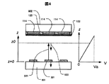
図4を用いて具体的に説明する。図4は、蛍光板602−陰極板601間の電位分布と電子の軌跡921、正イオンの軌跡922を模式的に示した図である。蛍光板602−陰極板601間は概ね均一電界が形成されているので、その電位分布は図4の右側のグラフに示したようになる。今、陰極板からの距離z=z0において正イオンが発生したとする。z=z0の電位をV(z0)とすると、この正イオンが軌跡922をたどって電子放出素子301に照射する際に、正イオンが持つ運動エネルギーはV(z0)である。したがって、蛍光板602−陰極板601間の空間のうち、蛍光板602に近い場所で発生したイオンほど高いエネルギーで電子放出素子301に入射する。
This will be specifically described with reference to FIG. FIG. 4 is a diagram schematically showing a potential distribution between the
図5は、MIM電子源を電子放出素子301に用いた画像表示装置を長時間動作させた際のダイオード電流の経時変化を示したものである。縦軸はダイオード電流を初期値で規格化した値(すなわち,初期のダイオード電流で除した値)をプロットしてある。蛍光面電圧Vaが200Vの場合には、長時間動作させてもダイオード電流はほぼ一定である。しかし,蛍光面電圧Vaを3KVにして動作させた場合は,ダイオード電流の経時変化量が増える。
FIG. 5 shows changes over time in the diode current when an image display apparatus using the MIM electron source as the electron-emitting
この劣化の原因を調べるために、蛍光面としてITO(indium tin Oxide)のみを成膜した表示パネル、すなわち、蛍光面に蛍光体を含まない表示パネルを作成して経時変化を調べた(図5で「3KV,ITO」と記載した特性)。その結果、蛍光体を含まないパネル(図5で「3KV,ITO」と記載)と、蛍光体を含む通常のパネル(図5で「3KV,Phosphor」と記載)とを比較すると、蛍光体を含むパネルではダイオード電流の経時変化量が更に大きい。この結果から、以下のことが判明した。 In order to investigate the cause of this deterioration, a display panel in which only an ITO (indium tin oxide) film is formed as a phosphor screen, that is, a display panel that does not contain a phosphor on the phosphor screen is prepared and the change with time is examined (FIG. 5). ("3KV, ITO"). As a result, when comparing a panel not containing the phosphor (described as “3KV, ITO” in FIG. 5) with a normal panel including the phosphor (described as “3KV, Phosphor” in FIG. 5), In the included panel, the amount of change over time of the diode current is even greater. From this result, the following was found.
正イオンの発生原因は主に2つある。第1は,蛍光体114であり、第2は表示パネル内にある微量の残留ガス分子である。蛍光体114にはエネルギーVaなる電子が照射するので、熱が発生したりして分子が脱離したり、電子衝撃による分子脱離や表面分解などが起こる。この際に発生した分子、原子に電子が照射するとイオンを発生する。さらに、蛍光面の電位は、図5に示したように、蛍光板602−陰極板601間で最大なので、蛍光体で発生した正イオンは電子放出素子301へ照射時の入射エネルギーが大きく、電子放出素子に与えるダメージが大きい。
There are two main causes for the generation of positive ions. The first is a
そこで、本発明の実施例1では、蛍光体114で発生した正イオンが電子放出素子に照射しないようにするために、蛍光体114と電子放出領域とを以下に記載するように適正配置する。
Therefore, in Example 1 of the present invention, the
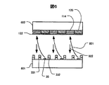
図6は、本発明の実施例1での表示パネルの断面図を模式的に示した図である。表示パネルは典型的には1000行×数千列のサブ画素から構成されるが、図6はそのうち3サブ画素のみ記載してある。ここで、サブ画素とは、カラー画像表示装置においてはカラー1画素を構成する赤色サブ画素、青色サブ画素、緑色サブ画素の各サブ画素に対応する。単色画像表示装置においては、1画素に対応する。陰極板601には,電子放出領域35を有する電子放出素子が形成されている。図6には、電子放出素子のうち電子放出領域35のみ記してある。
FIG. 6 is a diagram schematically showing a cross-sectional view of the display panel in Example 1 of the present invention. The display panel is typically composed of 1000 rows × several thousands of columns of subpixels, and FIG. 6 shows only three of them. Here, the sub-pixel corresponds to each of the red, blue, and green sub-pixels constituting one color pixel in the color image display device. In a monochrome image display device, this corresponds to one pixel. On the
本明細書において電子放出領域35とは、電子放出素子の構成部の中で電子を放出する部分を指す。薄膜電子源では、電子放出領域35は電子加速層上の上部電極に対応する。電界放射電子源では、電子放出領域35は電子放出エミッタ先端に対応する。図3に示した表面伝導型電子放出素子の場合,電子放出領域35は負極膜813と正極膜811に対応する。
In the present specification, the
1サブ画素内に複数の電子放出部位を有する構成の場合は、1サブ画素内の電子放出部位がある領域全体を電子放出領域35と定義する。例えば、非特許文献5に記載されているHEED型電子源の場合、1サブ画素内の上部電極内に、直径約1μmの電子放出部位が複数個含まれているが、この場合、1サブ画素内の電子放出部位全体を電子放出領域35と定義する。
In the case of a configuration having a plurality of electron emission sites in one subpixel, the entire region having the electron emission sites in one subpixel is defined as an
陰極板601にはビーム偏向電極A331とビーム偏向電極B332とが形成されている。ビーム偏向電極Aとビーム偏向電極Bとの間に電圧差を与えて電子放出領域35近傍の空間に横方向電界を発生させることで、電子放出領域35から放出された電子の軌道921を曲げる(偏向させる)。
On the
蛍光面602には蛍光体領域114とブラックマトリクス120とが形成されている。蛍光体領域114は、カラー画像表示装置においては、赤色蛍光体、緑色蛍光体、青色蛍光体の3種を塗り分ける。さらに、加速電極122を形成する。なお、蛍光板の製作方法は、後で実施例2に則して詳述する。電子ビームの軌道921が偏向しているのに対応して、蛍光体領域114の位置を電子放出領域35の位置からずらして配置してある。
A
本実施例の特徴は、蛍光体領域114と電子放出領域35との位置関係にある。図7は、蛍光体領域114と電子放出領域35を同一平面に投影して描いた平面図(投影平面図)である。図7からわかるように、投影平面図において、蛍光体領域114と電子放出素子の電子放出領域35とが重ならないように配置してある。蛍光面において、蛍光体領域114以外の領域はブラックマトリクス120を形成してあるので、別の見方をすると、投影平面図において電子放出領域35はブラックマトリクス120に含まれる。
The feature of this embodiment is the positional relationship between the
図6に示した通り,蛍光体領域114で発生した正イオンは正イオンの軌道922に沿って加速されて陰極板601に衝突する。正イオンの質量は電子の質量より1000倍以上大きいので,正イオンは横電界では殆ど軌道が曲がらずにほぼ直進するので、蛍光体領域114の直下の陰極板に衝突する。したがって、図6と図7に示したように蛍光体領域114と電子放出領域35とを配置すると、正イオンは電子放出領域35に照射せず、電子放出素子の劣化が起こらない。
As shown in FIG. 6, positive ions generated in the
なお、図6と図7では電子ビーム軌道921を偏向させる手段として、電子ビーム偏向電極A331とビーム偏向電極B332との電位差による横電界を用いているが、これは一例であって、軌道を偏向する別の方法を用いても同様の効果が得られる。例えば、後術する実施例で説明するように、陰極板601上に適正な電極形状を形成して電子レンズを構成することによりビームを偏向してもよい。また、本実施例に用いる電子放出素子301は、MIM型電子源を含む薄膜電子放出素子、表面伝導型電子放出素子、カーボンナノチューブ電子源を含む電界放射型電子放出素子の何れを用いても良い。
6 and 7, as a means for deflecting the
図8は、本発明の実施例1で用いる陰極板601の配線構造を示す平面図である。図8では、表示パネルのなかで3行×3列のサブ画素に対応する部分を示した。また、図8では、陰極板を構成する構成物のうち、電子放出領域35、ビーム偏向電極A331とビーム偏向電極B332、走査電極310のみを記載してある。
FIG. 8 is a plan view showing the wiring structure of the
各走査電極310は,片側(図8では上側)にビーム偏向電極A331が接続され、反対側にビーム偏向電極B332が接続されている。また、図8において、電子放出領域35−nに対応する電子放出素子301−n(図示せず)の一方の電極は走査電極310−nに電気的に接続されている。ここで、n=1〜3である。ここで、電子放出素子301の「一方の電極」とは,具体的には以下の通りである。薄膜電子源の場合は上部電極11である。図3の表面伝導型電子源の場合は正極膜811である。電界放射型電子源の場合はゲート電極である。
Each
図8には示していないが、データ電極311が走査電極310と直交する方向で配置されている。データ電極311は、電子放出素子301の他方の電極に電気的に接続されている。ここで電子放出素子301の「他方の電極」とは、具体的には以下の通りである。薄膜電子源の場合は下部電極13である。図3の表面伝導型電子源の場合は負極膜813である。電界放射型電子源の場合はエミッタ電極である。走査電極310−(n−1)と電子放出領域35−nに対応する電子放出素子301−nとは電気的に接続されていない。
Although not shown in FIG. 8, the
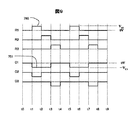
図9は、走査電極310−nへの印加電圧波形を示す図である。各走査電極には順次走査パルス750が印加される。走査パルス750は正の電圧振幅VR1を有する。走査パルス750が印加されている期間にデータ電極にデータパルス751が印加された電子放出素子301は電子放出領域35から電子を放出する。
FIG. 9 is a diagram illustrating a waveform of a voltage applied to the scan electrode 310-n. A
一例として、時刻t2〜t3の期間を考える。この期間では走査電極310−2に走査パルス750が印加されるので、電子放出領域35−2から電子が放出される。この際、走査電極310−2に接続されたビーム偏向電極A331には正の電圧VR1が印加されており、走査電極310−1に接続されたビーム偏向電極B332の電圧はゼロである。したがって、図6に記載されたように、電子放出領域35−2の近傍には横方向の電界が形成される。この電界により図6に示したように電子ビーム軌道921が偏向される。
As an example, consider the period from time t2 to t3. In this period, since the
なお、本実施例では走査パルス750として正極性のパルスを用いる場合を例として示した。走査パルスとして負極性のパルスを用いても同様の構成を実現できることは自明である。この場合、走査電極には電子放出素子の負極側の端子を接続し、データ電極には電子放出素子の正極側の端子を接続すればよい。
In this embodiment, the case where a positive pulse is used as the
本発明の実施例2は、電子放出素子として薄膜電子源を用いたものである。電界放射型陰極など他の電子源と比べて、薄膜電子源は放出電子ビームの空間的拡がりが小さい。その理由は以下の通りである。薄膜電子源では、電子加速層中で加速された電子が上部電極から真空中に放出される。薄膜電子源では、上部電極と下部電極とは互いに平行に対向配置されているため、電子加速層内の電界は平行電界である。この平行電界で電子が加速されるため、放出される電子の空間広がりが小さくなる訳である。放出電子ビームの空間的広がりが小さいことは、高精細の画像表示装置を実現できるという点で好ましい特性である。 Example 2 of the present invention uses a thin film electron source as an electron-emitting device. Compared to other electron sources such as a field emission cathode, the thin film electron source has a smaller spatial spread of the emitted electron beam. The reason is as follows. In the thin film electron source, electrons accelerated in the electron acceleration layer are emitted from the upper electrode into the vacuum. In the thin film electron source, since the upper electrode and the lower electrode are arranged to face each other in parallel, the electric field in the electron acceleration layer is a parallel electric field. Since electrons are accelerated by this parallel electric field, the spatial spread of the emitted electrons is reduced. A small spatial spread of the emitted electron beam is a preferable characteristic in that a high-definition image display device can be realized.
一方で、図4から分かるように、ビームの空間的広がりが小さいと、電子軌道921途上で発生した正イオンは、その大部分が電子放出領域35に照射されることになる。そのため、直進性に優れた薄膜電子源は正イオンによる電子源劣化の影響が大きく、その対策が必要である。本実施例では、薄膜電子源での耐イオン衝撃性を高めた画像表示装置を提供する。
On the other hand, as can be seen from FIG. 4, when the spatial spread of the beam is small, most of the positive ions generated in the
図10は、本発明の実施例2の表示パネルの断面図を模式的に示したものである。図10では、実施例2の特徴を明確にするために、構成の主要部のみを取り出して記載してある。薄膜電子源については、電子放出領域35のみを記載してある。詳細な構造は製造方法と合わせて後述する。また、図10に対応した平面図を図11に示した。図11のA−B間断面が図10に対応する。
FIG. 10 schematically shows a cross-sectional view of the display panel of Example 2 of the present invention. In FIG. 10, in order to clarify the features of the second embodiment, only the main part of the configuration is taken out and described. For the thin film electron source, only the
走査線310はコンタクト電極55を介して電子放出素子301の電極に電気的に接続されている。電子放出素子301は電子放出領域35を有する。図11では、走査線310−2が電子放出領域35−2を有する電子放出素子に接続されている。また、陰極板601には偏向電極315を設ける。偏向電極315は電子放出領域35より高い位置、すなわち膜厚を厚く形成し,陰極板601上で局所的な凸部を形成するようにする。
The
図10と図11に図示した点線G−H430は、隣接する偏向電極315の内側端面間距離(すなわち内法距離)の中点の位置を示す。すなわち、図11でd1=d2である。本明細書ではこのように定義されるG−H線430を中心線430と呼ぶことにする。本実施例の特徴は、局所的な凸部を形成する偏向電極間の中心線G−H430を電子放出領域35が含まないような位置に電子放出領域35を配置することである。このような配置をとることにより、後述の通り放出電子ビームを偏向できる。
A dotted line G-H430 illustrated in FIGS. 10 and 11 indicates the position of the midpoint of the distance between the inner end faces of adjacent deflection electrodes 315 (that is, the internal distance). That is, d1 = d2 in FIG. In this specification, the
本実施例でのビーム偏向メカニズムを図12を用いて述べる。図12には偏向電極の周期構造により形成される等電位面441を点線で模式的に示した。この等電位面441が形成する電子レンズは、電子放出領域35から放出した電子ビームを中心線430の方向に偏向する。説明のために、図12には仮想的に仮想電子放出領域435を配置し、仮想電子放出領域435から放出された電子ビームの軌道921‐2も示した。ビーム軌道921‐2も中心線430の方向に偏向する。
The beam deflection mechanism in this embodiment will be described with reference to FIG. In FIG. 12, the
このことから、中心線430を跨がないように電子放出領域35を配置すれば、放出電子が軌道921のように偏向することが分かる。これが本発明での電子ビームの偏向原理である。
From this, it can be seen that if the
なお,図12に記したように、電子放出領域からの放出ビーム軌道921と仮想電子放出領域435からの放出ビーム軌道921‐2はクロスオーバー(交差点)を持つように電極形状を設計することが望ましい。このようにすると、仮想電子放出領域435を除いた実際の構成ではビーム偏向量が大きくなり、正イオンが電子放出領域に入射することを更に防止できる。
As shown in FIG. 12, it is possible to design the electrode shape so that the
電子ビーム軌道を偏向させる役割を果たす電子レンズの特性を決める主な要因は、(a)偏向電極と上部電極との高さの差、(b)偏向電極と上部電極との電圧差、(c)偏向電極の周期(隣接する偏向電極間の距離)、(d)蛍光面電圧Va、の4つである。要因(a)「偏向電極と上部電極との高さの差」は図12からわかるように、電子レンズ特性を決める大きな要因である。高さの差が大きいほどビーム偏向量は大きくなる。 The main factors that determine the characteristics of the electron lens that plays the role of deflecting the electron beam trajectory are: (a) the difference in height between the deflection electrode and the upper electrode, (b) the voltage difference between the deflection electrode and the upper electrode, (c ) Deflection electrode period (distance between adjacent deflection electrodes) and (d) phosphor screen voltage Va. Factor (a) “the difference in height between the deflection electrode and the upper electrode” is a major factor that determines the characteristics of the electron lens, as can be seen from FIG. The greater the difference in height, the greater the amount of beam deflection.
ここで、電極の「高さ」とは,陰極板601を構成する基板14の表面から測った高さであり、基板14表面から電極の最も高い部位(最高部)までの長さとして定義する。すなわち、後述する図30(a)のように,基板14に偏向電極315が直接形成される場合には、その膜厚が高さh0になる。また、図30(b)のように、誘電体385の上に偏向電極315が形成される場合には、偏向電極315の最も高い位置までの長さ(図中のh0)が高さを定義する。上部電極の「高さ」も同様に定義する。図30(b)のような場合でも,高さh0が電子レンズ特性を主に支配する。
Here, the “height” of the electrode is a height measured from the surface of the
図12の説明から分かるように、本実施例では、電子放出領域の両側に、電子放出領域よりも高い位置に偏向電極があることにより、横方向電界が形成され、電子放出領域から放出された電子ビームの軌道が偏向する。十分なビーム偏向量を得るには,偏向電極は上部電極の高さの高さより2μm以上高くすることが望ましい。 As can be seen from the description of FIG. 12, in this embodiment, the lateral electrodes are emitted from the electron emission region due to the deflection electrodes on both sides of the electron emission region at positions higher than the electron emission region. The electron beam trajectory is deflected. In order to obtain a sufficient beam deflection amount, it is desirable that the deflection electrode be 2 μm or more higher than the height of the upper electrode.
図12の説明から分かるように、偏向電極の周期(隣接する偏向電極間の距離)も電子レンズ特性に影響する。この周期をサブ画素の周期と一致させると、各サブ画素のビーム偏向量が一定になるので好ましい。 As can be seen from the description of FIG. 12, the period of the deflection electrode (distance between adjacent deflection electrodes) also affects the electron lens characteristics. It is preferable to make this period coincide with the period of the sub-pixel because the beam deflection amount of each sub-pixel becomes constant.
また、図12の説明から分かるように、上部電極高さより高い位置にある電極(「突起電極」と呼ぶ)が上部電極の近傍に周期的に配置されていればよい。したがって、偏向電極とは別の役割を持った電極であっても、その電極(突起電極)が上部電極と十分な高低差を有し、かつ周期的に配置されているものであれば、それを偏向電極と見なすことができる。本実施例では、そのような場合は、その突起電極が偏向電極の役割を兼ねていると見なし、その突起電極を偏向電極とみなす。 Further, as can be seen from the description of FIG. 12, it is only necessary that the electrodes (referred to as “projection electrodes”) located higher than the height of the upper electrode are periodically arranged in the vicinity of the upper electrode. Therefore, even if the electrode has a role different from that of the deflection electrode, if the electrode (projection electrode) has a sufficient height difference from the upper electrode and is periodically disposed, Can be regarded as deflection electrodes. In this embodiment, in such a case, it is considered that the protruding electrode also serves as the deflection electrode, and the protruding electrode is considered as the deflection electrode.
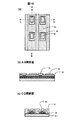
次に、本実施例の画像表示装置をより詳細に説明する。先ず、画像表示装置を構成する表示パネル100の作成方法を説明する。表示パネル100は陰極板601と蛍光板602とで構成される。図13は、陰極板601の一部を示した平面図である。図13では2行×2列のサブ画素を取り出して図示した。図14は陰極板601の一部を示した断面図である。図13のA−B間断面図が図14(a)に対応し、C−D間断面図が図14(b)に対応する。なお、図13は上部電極11を取り除いた平面図になっている。実際には、図14の断面図からわかるように上部電極11が全面に成膜されている。
Next, the image display apparatus of the present embodiment will be described in more detail. First, a method for creating the display panel 100 constituting the image display apparatus will be described. The display panel 100 includes a
図13は、図12において電子放出素子301として薄膜電子源を用いた場合の具体的構成例を詳細に記したものである。したがって、図13では,電子放出素子301と電極配線との接続関係は図12に対応した形になっている。以下、電子放出素子301‐nに対応する電子放出領域35を35−nと記すことにする。すると、図12の記号を用いて述べると、電子放出素子301‐2へは走査線310‐2からコンタクト電極55を介して給電されており、隣接する走査線310‐1(図13ではバス電極32に対応)からは偏向電極315が電子放出領域35−nの長辺に沿って設置されている。本実施例では偏向電極315を走査線310と電気的に接続することにより,配線を簡略にする利点がある。
FIG. 13 shows a detailed configuration example in the case where a thin film electron source is used as the electron-emitting
陰極板601の構成は以下の通りである。図14において、ガラスなどの絶縁性の基板14上に、下部電極13、絶縁層12、上部電極11とで構成される薄膜電子源301(本実施例における電子放出素子301)が構成される。バス電極32は、コンタクト電極55を介して上部電極11に電気的に接続されている。バス電極32は上部電極11への給電線として働く。すなわち,駆動回路からこのサブ画素の位置まで電流を運ぶ働きをしている。また、本実施例ではバス電極32は走査電極310として働く。
The configuration of the
本実施例では電子放出素子301として薄膜電子源を用いている。図14に示したように下部電極13、トンネル絶縁層12、上部電極11の3つが薄膜電子源の基本構成である。図13の電子放出領域35はトンネル絶縁層12に対応した場所である。電子放出領域35の上部電極11表面から電子が真空中に放出される。
In this embodiment, a thin film electron source is used as the electron-emitting
本実施例ではデータ線311の一部の領域(トンネル絶縁層12に接する領域)が下部電極13となっている。本明細書では、データ線311のうち、トンネル絶縁層12に接する部分を下部電極13と呼ぶ。各サブ画素の対応する部分には3重の長方形が配置されている。一番内側の長方形領域は、電子放出領域35を示しており、これは第1層間絶縁膜15のテーパー部(傾斜領域部)の再内周に相当する。その外側の長方形は第1層間絶縁膜15のテーパー膜の再外周に相当する。その外側(再外周)は第2層間絶縁層51の開口部である。
In this embodiment, a part of the data line 311 (a region in contact with the tunnel insulating layer 12) is the
本実施例では走査電極310はバス電極32により構成されている。また、本実施例では、走査電極310上にスペーサ60を設置している。スペーサ60は全ての走査電極上に設置する必要はなく、走査電極何本か毎に設置すればよい。スペーサ60は走査電極310に電気的に接続されており、蛍光板602の加速電極122からスペーサ60を介して流れる電流を流す働きと、スペーサ60に帯電した電荷を流す働きをする。なお、図14では高さ方向の縮尺は任意である。すなわち、下部電極13や上部電極などは数μm以下の厚さであるが、基板14と面板110との距離は1〜3mm程度の長さである。
In this embodiment, the
図13において、隣り合う偏向電極315の内端の間の距離を2等分する位置にある線G−Hを中心線430と呼ぶ。すなわち、図13においてd1=d2である。電子放出領域35は中心線430をまたがないように配置されているのが、本実施例の特徴である。
In FIG. 13, a line GH at a position that bisects the distance between the inner ends of
陰極板601の作成方法を図15〜図23を用いて説明する。図15〜図23は基板14上に薄膜電子源を作製するプロセスを示したものである。これらの図には2×2個のサブ画素に対応する薄膜電子源を記載してある。各図の(a)は平面図であり、A−B間の断面図を(b)に、C−D間の断面図を(c)に示してある。
A method for producing the
ガラスなどの絶縁性基板14上に、下部電極13(データ線311)用の材料として、Al合金を例えば300nmの膜厚に形成する。ここではAl‐Nd合金を用いた。このAl合金膜の形成には、例えば、スパッタリング法や抵抗加熱蒸着法などを用いる。次に、このAl合金膜を、フォトリソグラフィによるレジスト形成と、それに続くエッチングとによりストライプ状に加工し下部電極13を形成する。ここで用いるレジストはエッチングに適したものであればよく、また、エッチングもウエットエッチング、ドライエッチングのいずれも可能である。
On the insulating
次に、レジストを塗布して紫外線で露光してパターニングし、図15のレジストパターン501を形成する。レジストには、例えばキノンジアザイド系のポジ型レジストを用いる。次に、レジストパターン501を付けたまま陽極酸化を行い、第1層間絶縁層15を形成する。この陽極酸化は、本実施例では化成電圧100V程度とし、第1層間絶縁層15の膜厚を140nm程度とした。この後レジストパターン501を剥離する。これが、図16の状態である。
Next, a resist is applied and exposed to ultraviolet light for patterning to form a resist
次に、レジスト501で被覆されていた下部電極13表面を陽極酸化して絶縁層12を形成する。本実施例では化成電圧を4Vに設定し、絶縁層膜厚を9.7nmとした。これが図17の状態である。絶縁層12が形成された領域が電子放出領域35になる。すなわち、第1層間絶縁層15に囲まれた領域が電子放出領域35である。
Next, the surface of the
なお、アルミニウムを陽極酸化して得た陽極酸化絶縁膜の膜厚dは,膜厚が20nm程度よりも薄い場合にはd(nm)=1.36×(VAO+1.8)なる関係が成立することが示されている(「非特許文献3」)。この関係式から化成電圧4Vの場合の絶縁層膜厚を求めると7.9nmになる。しかし、透過型電子顕微鏡による膜厚測定で測定した結果、化成電圧4Vで生成する膜厚は9.7nmであることがわかった。上記の膜厚値は、この実測値を用いている。
Note that the film thickness d of the anodized insulating film obtained by anodizing aluminum satisfies the relationship d (nm) = 1.36 × (VAO + 1.8) when the film thickness is thinner than about 20 nm. ("
次に、以下の手順により第2層間絶縁層51および電子放出領域保護層52を形成する(図18)。第2層間絶縁層51のパターンは、バス電極32とデータ電極311との交差領域に形成し、電子放出領域35は露出するパターンにする。但し、図18の工程段階では、電子放出領域35は電子放出領域保護層52で覆われている。第2層間絶縁層51および電子放出領域保護層52は,窒化シリコンSiNxや酸化シリコンSiOxなどを成膜した後、エッチングによりパターン化する。本実施例では100nm膜厚の窒化シリコン膜を用いた。エッチングは、例えばCF4やSF6を主成分とするエッチング剤を用いたドライエッチングによって行う。
Next, the second
第2層間絶縁層51は、走査電極とデータ電極との間の絶縁性を高めるために形成する。電子放出領域保護層52は電子放出領域35となる部分(すなわち絶縁層12)を後続の工程でのプロセスダメージから保護するためのものであり、後述する通り、後の工程で取り除く。本実施例では、第2層間絶縁層51と電子放出領域保護層52は同一材料、同一工程で形成する。
The second
次に、コンタクト電極55、バス電極32、バス電極上層34を構成する材料を、この順に成膜する(図19)。本実施例ではコンタクト電極55にはクロム(Cr)100nm厚を用い、バス電極32にはアルミニウム(Al)10μm厚を用い、バス電極上層34にはクロム(Cr)200nm厚を用いた。これらの電極はスパッタリングで成膜した。バス電極32の材料は,導電性が高い材料を用いると、配線抵抗が低くなり、電極での電圧降下を低減できるので好ましい。
Next, the materials constituting the
次に、バス電極上層34およびバス電極32をエッチングによりパターン化し、後に上部電極11がコンタクト電極55と接続できるように露出させ、バス電極32を形成する(図20)。この工程で偏向電極315を同時に形成する。図20(a),図20(c)に示したように,バス電極32に突起部を設けたパターンを用いることで,その突起部を偏向電極315として用いる。すなわち,バス電極32と偏向電極315とは同一材料である。このようにすると、従来と同じ製造工程でつくることが出来るという利点がある。
Next, the bus electrode
次に、コンタクト電極55をエッチングによりパターン化する(図21)。ここでのコンタクト電極55のパターン化により、コンタクト電極55から電子放出領域35への給電状態が決定される。図21(a)に示した通り、コンタクト電極55は電子放出領域35の4辺のうち、長辺を含む2辺が沿うパターンにしてある。上述の通り、電子放出領域35の長辺を含む2辺給電構造とすることで給電能力を向上させている。
Next, the
図21(b)の断面図に矢印で示した通り、コンタクト電極55の片側(図中,矢印で示した部位)は、バス電極32に対してアンダーカットを形成し、後の工程で上部電極13を電気的に分離するための庇を形成する。このアンダーカットの存在により、隣接する走査線に接続されたサブ画素の上部電極が互いに電気的に絶縁(分離)される。これを「画素分離」と呼ぶ。バス電極32と偏向電極315とは同一プロセスで作成しているため、走査電極315の下にもアンダーカットが形成されており、隣接走査線と電気的に絶縁されている。
As shown by the arrow in the cross-sectional view of FIG. 21B, one side of the contact electrode 55 (the part indicated by the arrow in the figure) forms an undercut with respect to the
コンタクト電極55のアンダーカット量は以下のようにして制御する。アンダーカットを形成する部分は、バス電極32の辺をフォトマスクとして用いてコンタクト電極55をエッチングする。したがって、コンタクト電極55は、バス電極32に対してアンダーカットが発生する。一方、アンダーカット量が大きすぎると、バス電極32が崩落してバス電極32と第2層間絶縁層51とが接触し、庇がなくなってしまう。そこで過大なアンダーカット形成を防ぐために、コンタクト電極55の材料として、標準電極電位がバス電極32材料よりも貴な材料を用いる。すなわち、コンタクト電極55として、バス電極32材料よりも標準電極電位が高い材料を用いる。
The undercut amount of the
バス電極をアルミニウムとする場合、このような材料として例えばクロム(Cr)、モリブデン(Mo)、あるいはCr合金など、これらを成分として含む合金、例えばモリブデン−クロム−ニッケル(Mo−Cr−Ni)合金がある。このようにすると、局部電池作用によりコンタクト電極55のサイドエッチが途中で停止するためアンダーカット量が増えすぎることを防止できる。さらに、標準電極電位が卑な(低い)材料であるバス電極のエッチング液への露出面積を制御することで、局部電池作用を制御しコンタクト電極55のサイドエッチの停止位置(すなわち、アンダーカット量)を制御できる。この目的で、クロム(Cr)を材料とするバス電極上層34が形成してある。
When the bus electrode is made of aluminum, examples of such a material include chromium (Cr), molybdenum (Mo), or a Cr alloy, and an alloy containing these as components, such as a molybdenum-chromium-nickel (Mo-Cr-Ni) alloy. There is. If it does in this way, since side etching of
以上の記載からわかるように、コンタクト電極55の材料は、バス電極32の材料よりも標準電極電位が貴な(高い)ものを用いることが好ましい。
As can be seen from the above description, it is preferable to use a material for the
次に、ドライエッチングなどにより電子放出領域保護層52を除去する(図22)。次に、上部電極11を形成して陰極板601が完成する(図23)。本実施例では、上部電極11としてイリジウム(Ir)、白金(Pt)、金(Au)の積層膜を用いた。上部電極11はスパッタ成膜で形成した。なお、実際には全面に上部電極11が成膜されているが、構成をわかりやすくする目的で、図23(a)では上部電極を取り除いた図を記してある。また、データ線311の位置を点線で記してある。
Next, the electron emission region
図23に示した通り、給電線であるバス電極32からコンタクト電極55を経由して電子放出領域35の上部電極11に電流が供給される。一方、前述の通り、コンタクト電極55には適切な量のアンダーカットが形成されているため、隣接する走査電極310間で互いに電気的に絶縁されている。
As shown in FIG. 23, a current is supplied from the
本実施例では、バス電極32から電子放出領域35の上部電極11への給電経路として電子放出領域の長辺を含む2辺を用いるという特徴(特徴A)と、バス電極から電子放出領域の上部電極への給電経路から第2層間絶縁層の段差部を無くしたという特徴(特徴B)という、2つの特徴を取り入れた陰極構造を採用している。
In the present embodiment, a feature (feature A) in which two sides including the long side of the electron emission region are used as a power feeding path from the
蛍光板602の構成は以下の通りである。図14に示した通り、ガラスなど透光性の面板110にはブラックマトリクス120が形成され,さらに各電子放出領域に対向する位置に蛍光体114が形成されている。カラー画像表示装置の場合は、蛍光体114として赤色蛍光体、緑色蛍光体、青色蛍光体を塗り分ける。さらに、加速電極122が形成されている。加速電極122は膜厚70nm〜100nm程度のアルミ膜で形成されており、薄膜電子源301から放出された電子は、加速電極122に印加された加速電圧で加速された後、加速電極122に入射すると、加速電極を透過して蛍光体114に衝突し、蛍光体を発光させる。蛍光板602の作成方法の詳細は、例えば特開2001‐83907に記載されている。
The configuration of the
図10に示した通り、本実施例では放出された電子の軌道は偏向するので、蛍光体領域114の位置は電子放出領域35の直上には配置せず、ビームの偏向量を考慮して配置する。すなわち、電子放出領域35の中心位置と蛍光体領域114の中心位置とをずらすことになる。陰極板601と蛍光板602との間には、スペーサ60が適当な個数配置されている。図1に示したとおり、陰極板601と蛍光板602とは枠部材603を挟んで封着される。さらに、陰極板601と蛍光板602と枠部材603とで囲まれた空間は真空に排気される。以上の手順で表示パネルが完成する。
As shown in FIG. 10, since the emitted electron trajectory is deflected in this embodiment, the position of the
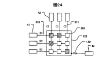
図24は,このようにして製作した表示パネル100の駆動回路への結線図である。走査電極310は走査電極駆動回路41へ結線し、データ電極311はデータ電極駆動回路42に結線する。加速電極122は抵抗130を経由して加速電極駆動回路43へ結線する。n番目の走査電極310Rnとm番目のデータ電極311Cmの交点のドットを(n,m)で表すことにする。
FIG. 24 is a connection diagram to the drive circuit of the display panel 100 manufactured as described above.
抵抗130の抵抗値は以下のように設定した。例えば、対角寸法51cm(公称20インチ)の表示装置では表示面積は1240cm2である。加速電極122と陰極との間の距離を2mmに設定した場合、加速電極122と陰極との間の静電容量Cgは約550pFとなる。真空放電の発生時間(20ナノ秒程度)よりも充分長い時定数、例えば500ナノ秒とするために、抵抗130の抵抗値Rsは900Ω以上に設定すればよい。本実施例では18KΩに設定した(時定数10μs)。このように時定数Rs×Cg>20nsを満足する抵抗値の抵抗を加速電極122と加速電極駆動回路43の間に挿入することにより、表示パネル内での真空放電の発生を抑制する効果がある。
The resistance value of the
図25は、各駆動回路の発生電圧の波形を示す。図25には記されていないが、加速電極122には3〜10KV程度の電圧(蛍光面電圧Va)を印加する。時刻t0ではいずれの電極も電圧ゼロであるので電子は放出されず、したがって,蛍光体114は発光しない。
FIG. 25 shows the waveform of the voltage generated by each drive circuit. Although not shown in FIG. 25, a voltage of about 3 to 10 KV (phosphor screen voltage Va) is applied to the
時刻t1において、走査電極310R1にはVR1=Vsなる電圧の走査パルス750を印加して選択状態にする。走査電極310R1以外の選択されていない走査線にはVnsなる電圧を印加する。本実施例ではVns=0Vとした。また,時刻t1において、データ電極311C1,C2には−VC1なる電圧のデータパルス751を印加する。ドット(1,1),(1,2)の下部電極13と上部電極との間には(VC1+VR1)なる電圧が印加されるので,(VC1+VR1)を電子放出開始電圧以上に設定しておけば、この2つのドットの薄膜電子源からは電子が真空10中に放出される。
At time t1, a
本実施例では、VR1=Vs=+4V,−VC1=−3Vとした。放出された電子は加速電極122に印加された電圧により加速された後、蛍光体114に衝突し、蛍光体114を発光させる。時刻t2において、走査電極310R2にVR1=Vsなる電圧を印加し、データ電極311C1に−VC1なる電圧を印加すると,同様にドット(2,1)が点灯する。このようにして、図25の電圧波形を印加すると、図24の斜線を施したドットのみが点灯する。
In this embodiment, V R1 = Vs = + 4 V, −V C1 = −3 V. The emitted electrons are accelerated by the voltage applied to the accelerating
このようにして、データ電極311に印加する信号を変えることにより所望の画像または情報を表示することができる。また、データ電極311への印加電圧−VC1の大きさを画像信号に合わせて適宜変えることにより、階調のある画像を表示することができる。
In this manner, a desired image or information can be displayed by changing a signal applied to the
図25に示したように、時刻t4において全ての走査電極310に−VR2なる電圧を印加する。本実施例では−VR2=−3Vとした。このとき全てのデータ電極311への印加電圧は0Vなので、薄膜電子源301には−VR2=−3Vの電圧が印加される。このように電子放出時とは逆極性の電圧(反転パルス754)を印加することにより絶縁層12内のトラップに蓄積した電荷を解放し、薄膜電子源の寿命特性を向上できる。また、反転パルスを印加する期間(図25のt4〜t5,t8〜t9)としては、映像信号の垂直帰線期間を用いると、映像信号との整合性が良い。図24と図25での説明では、簡単のため3×3ドットの例を用いて説明したが、実際の画像表示装置では走査電極数が数100〜数千本、データ電極数も数100〜数千本ある。
As shown in FIG. 25, a voltage of −V R2 is applied to all the
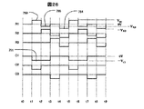
図26は、別の駆動方法を示したものである。この駆動方法では、時刻t2〜t3の期間において走査電極310R2に走査パルス750を印加し、走査電極310R2に接続された電子放出素子に隣接する走査電極310R1には偏向パルス755を印加する。偏向パルスの電圧はVdef=−VR3とする。このようにして偏向電極315の電圧を適正に設定することで、偏向電極315、コンタクト電極55、上部電極11の電圧関係を最適化し、一層高いビーム偏向効果を得ることができる。
FIG. 26 shows another driving method. In this driving method, the
図10から分かるように、電子ビーム軌道を偏向させる電子レンズは、蛍光面電圧、偏向電極の電圧、上部電極の電圧が影響する。電子放出時の上部電極−偏向電極間電圧は、図25の駆動方法においては(Vs−Vns)であり、図26の駆動方法においては(Vs−Vdef)である。電子軌道シミュレーションを行った結果、(Vs−Vdef)が大きいほどビーム偏向量は大きい。したがって、ビーム偏向量を大きくしたい場合は,(Vs−Vdef)の絶対値を(Vs−Vns)の絶対値より大きくすると良い。また、より好ましい実施の形態として、偏向パルス755の電圧−VR3を反転パルス754の電圧−VR2と等しく設定する。このように設定すると、駆動回路が簡略化されるのでより好ましい。
As can be seen from FIG. 10, the electron lens for deflecting the electron beam trajectory is affected by the phosphor screen voltage, the deflection electrode voltage, and the upper electrode voltage. The voltage between the upper electrode and the deflection electrode at the time of electron emission is (Vs−Vns) in the driving method of FIG. 25 and (Vs−Vdef) in the driving method of FIG. As a result of the electron orbit simulation, the larger the (Vs−Vdef), the larger the beam deflection amount. Therefore, when it is desired to increase the beam deflection amount, the absolute value of (Vs−Vdef) is preferably made larger than the absolute value of (Vs−Vns). As a more preferred embodiment, the voltage −V R3 of the
本実施例の更に好ましい形態として、蛍光体領域144と電子放出領域35の関係を説明する。前述の通り、蛍光体は正イオンの発生を起こしやすい場所であるから、蛍光体領域144を電子放出領域35とは、投射平面図において互いに重ならないように配置すると、正イオンの発生と電子放出領域への照射を一層低減できるので更に好ましい。すなわち、図10において、d3>0,d4>0とすると更に好ましい。条件「d3>0」は、電子放出領域に対応する蛍光体領域144が重ならない条件であり、条件「d4>0」は、隣接蛍光体領域144が電子放出領域と重ならない条件である。
As a more preferable embodiment of the present embodiment, the relationship between the phosphor region 144 and the
本実施例では、偏向電極315は,走査線310(すなわち、バス電極32)と同一材料を用い、同一フォト工程で同時にパターン化する。このようにすることで、偏向電極を導入してもマスク枚数を増やすことなく、従来と同一の製造プロセスで製造できるので、好ましい。
In this embodiment, the deflecting
本発明の実施例3を図27と図28を用いて説明する。図27は、本実施例で用いる表示パネル100を構成する陰極板601の平面図である。図28は、陰極板601の断面図であり、図28(a)は図27のA−B間断面、(b)はC−D間断面を示す。実施例3と前述の実施例2(図13、図14)とを比べると、本実施例ではコンタクト電極55の形状が異なる。図13ではコンタクト電極55は電子放出領域35の長辺に沿って延びた枝上の張り出し部を有しているが、本実施例(図27)ではその張り出し部がない。
A third embodiment of the present invention will be described with reference to FIGS. FIG. 27 is a plan view of the
図28(b)から分かるように、上部電極11は走査電極310(すなわち、バス電極32)と偏向電極315以外は、ほぼ全面に形成されている。コンタクト電極55の膜厚(本実施例では0.1μm厚)は偏向電極315の膜厚10μmの1/100なので、コンタクト電極の形状は電子放出領域35近傍の電界分布にあまり影響しない。したがって、図27と図28の電極形状でも,前実施例と同様なビーム偏向効果が得られる。
As can be seen from FIG. 28B, the
本実施例(図27)では、コンタクト電極の形状が単純なので製造しやすいという利点がある。特にコンタクト電極のパターン化の際、横方向のマスク合わせに高い精度が必要なくなるので作りやすい。一方、図13のコンタクト電極形状は、給電能力が高く薄膜電子源の電子放出効率を高めたり、信頼性を高めたりできる利点がある。この点を図29を用いて説明する。コンタクト電極55は、走査線310(本実施例ではバス電極32で構成される)と上部電極11を電気的に接続する役割がある。薄膜電子源では電子放出領域35全体に電流を供給しなければならないが、上部電極11は10nm以下程度と薄いので抵抗が高い。そこで、膜厚が100nm程度として抵抗を低くしたコンタクト電極55を経由して電流を給電するわけである。
In this embodiment (FIG. 27), there is an advantage that the shape of the contact electrode is simple and easy to manufacture. In particular, when patterning the contact electrode, it is easy to make it because high accuracy is not required for the horizontal mask alignment. On the other hand, the shape of the contact electrode in FIG. 13 has an advantage that the power supply capability is high and the electron emission efficiency of the thin film electron source can be increased or the reliability can be improved. This point will be described with reference to FIG. The
コンタクト電極形状と給電能力との関係を図29を用いて説明する。図29は電子放出領域35、コンタクト電極55、走査電極310(本実施例ではバス電極32で構成される)の配置を模式的に示したものである。図29(a)は図27の実施例に対応し、(b)は図13の実施例に対応する。
The relationship between the contact electrode shape and the power supply capability will be described with reference to FIG. FIG. 29 schematically shows the arrangement of the
図29(a)のコンタクト電極形状では、電流は電子放出領域35のひとつの辺871のみから給電されるので電流が辺871に集中するため、上部電極11に流れる電流密度が比較的大きい。一方、図29(b)のコンタクト電極形状では,電流は電子放出領域35の二つの辺871,872から給電されるので電流が分散する。このため、上部電極11に流れる電流密度が減少し、上部電極に要求される抵抗値が高くても許容される。このため、上部電極膜厚を薄くすることが可能になる。上部電極を薄くすると、上部電極内でのホットエレクトロンの非弾性散乱が減るため、電子放出効率が高くなる。また、電流が分散するため、コンタクト電極と上部電極との間の接続信頼性が高まる。
In the contact electrode shape of FIG. 29A, since the current is fed from only one
カラー画像表示装置では、多くの場合、赤色、緑色、青色のサブ画素を横方向に配置して1画素を構成する。1画素はほぼ正方形であるから、各サブ画素の形状は縦長になることが一般的である。これに対応して、各サブ画素に対応する電子放出領域35の形状も縦長にする。この理由により,カラー画像表示装置では,図29のb0/a0比は通常1より大きく,典型的には2〜3である。このため、図29(a)では電子放出領域35の短い方の辺(短辺)に電流が集中することになる。図29(b)では、長さb0の長辺からも電流を供給するので,電流が分散される。このように、電子放出領域35の長辺に沿ってコンタクト電極55を配置すると、上部電極に流れる電流密度が減少し、より好ましい。
In many color image display devices, red, green, and blue sub-pixels are arranged in the horizontal direction to form one pixel. Since one pixel is substantially square, the shape of each subpixel is generally vertically long. Correspondingly, the shape of the
本発明の実施例4を図31を用いて説明する。本実施例は薄膜電子源を電子放出素子として用いたものである。図31は、表示パネルを構成する陰極板601の平面図であり、主な構成要素のみ記した図ある。図31は前述の実施例の図11に対応するものである。図31では、陰極板601を構成する要素のうち、走査線310、コンタクト電極55、各電子放出素子301の電子放出領域35のみを記載してある。電子放出領域35−2はコンタクト電極55を介して走査線310−2に電気的に接続されている。
A fourth embodiment of the present invention will be described with reference to FIG. In this embodiment, a thin film electron source is used as an electron-emitting device. FIG. 31 is a plan view of the
本実施例では、走査線301の膜厚を厚さ6μmとすることで,走査線301の高さを上部電極高さより十分高くし、走査線301に偏向電極の働きを兼用させるものである。図31に示す通り、隣接する走査線301間の内端の距離の中心線G−H430を含まないように、電子放出領域35を配置する。このようにすることで、電子放出領域から放出した電子が(図面の)上下方向に偏向する。
In this embodiment, by setting the thickness of the
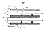
ここで電極の「高さ」とは,前述の通り図30で定義される値である。すなわち,図30(a)のように、基板14に偏向電極315が直接形成される場合には、その膜厚が高さh0になる。また、図30(b)のように、誘電体385の上に偏向電極315が形成される場合には、偏向電極315の最も高い位置までの長さ(図中のh0)が高さを定義する。図30では偏向電極315の高さを示しているが,走査線301の高さは,図30で偏向電極315を走査線301に読み替えて定義する。図30(b)のような場合でも,高さh0が電子レンズ特性を主に支配する。
Here, the “height” of the electrode is a value defined in FIG. 30 as described above. That is, as shown in FIG. 30A, when the
本実施例では,走査線301に図11のような偏向電極315の張り出し部を設けることなく,走査線301自体の高さを利用して偏向電極の働きを持たせている。実施例2と比較すると,配線パターンが単純なため製作しやすいという利点がある。
In this embodiment, the
一方,実施例2では,図11に示すように,偏向電極315が走査線301と平行な軸に沿って周期的に配置されている。すなわち,偏向電極315が周期的に配置されているが,この繰り返し方向が走査線301と平行である。これにより電子ビームは図10に示したように,走査線301と平行な方向に偏向する。この方向にビームを偏向させることの主な利点は2つある。
On the other hand, in the second embodiment, as shown in FIG. 11, the
第1は,隣接する偏向電極315間の距離(周期)が短いことである。偏向電極315間の距離が短いほど,電子レンズ効果が強まるため,電子ビームの偏向量が増える。このため,イオン照射の影響をより低減できる。そして,前述の通り,カラー画像表示装置においては,サブ画素を水平方向に配置することが多いため,図11のように偏向電極315を走査線301と平行な軸に沿って周期的に配置した方が,偏向電極間の距離が短くなる。
The first is that the distance (period) between
第2は,スペーサ60と平行な方向に電子ビームを偏向させることで,スペーサの帯電を防ぐ上で好ましいということである。スペーサ60が帯電すると表示パネル内の電界が歪むため,電子ビームが所望の経路からはずれ,表示画像に悪影響する場合がある。電子ビームの偏向方向がスペーサ60と平行方向であれば,スペーサの帯電を防げる。そして,典型的な表示パネルでは,図13に示したように,スペーサ60は走査線301(バス電極32,34)と平行方向に配置される。したがって,図11のように偏向電極315を走査線301と平行な軸に沿って周期的に配置することで,ビーム偏向の方向がスペーサ60と平行な方向になる。
Second, it is preferable to prevent the spacer from being charged by deflecting the electron beam in a direction parallel to the
本発明の実施例5を図32と図33を用いて説明する。実施例5は薄膜電子源を電子放出素子として用いたものである。図32は、本実施例の画像表示装置で用いる表示パネル100の一部の断面図である。また、図33は、対応する平面図である。図33のA−B間断面図が図32である。図32では、薄膜電子源で構成される電子放出素子301については、その電子放出領域35のみ記載してある。薄膜電子源の内部構造、すなわち上部電極11、電子加速層12、下部電極13という内部構造、および層間絶縁膜やデータ線などの詳細な配線構造は記載を省略してある。これらの詳細構造は前述した実施例2と同様である。
A fifth embodiment of the present invention will be described with reference to FIGS. 32 and 33. FIG. Example 5 uses a thin-film electron source as an electron-emitting device. FIG. 32 is a cross-sectional view of a part of the display panel 100 used in the image display apparatus of the present embodiment. FIG. 33 is a corresponding plan view. FIG. 32 is a cross-sectional view taken along the line AB in FIG. In FIG. 32, only the
図33の平面図は、走査線310、コンタクト電極55、電子放出領域35、遮蔽電極371の位置関係を示す概略平面図であり、その他の構成要素は図示を省略した。図32では、電子放出領域35を構成要素とする電子放出素子301の上部電極11は、コンタクト電極55を介して走査線310に電気的に接続されている。走査線310の高さは10μmである。走査線310の上には誘電体層372が配置され、その上には遮蔽電極371が設置されている。遮蔽電極371は電子放出領域35の直上に張り出しており、その張り出し長さL2は50μmである。誘電体層372の膜厚T2は100μmである。陰極板601と蛍光板602との距離L0は3mmとした。蛍光面電圧Vaは10KVとした。この条件における電子放出領域35から放出された電子ビームの軌道をシミュレーションで求めたものが電子軌道921である。電子放出領域35から放出した電子ビームは蛍光板602に達すると400μm偏向する。そして、蛍光体114に照射し蛍光体を発光させる。
The plan view of FIG. 33 is a schematic plan view showing the positional relationship among the
本実施例の特徴は、遮蔽電極371と電子放出領域35を同一平面に投射した投射平面図において、電子放出領域35が遮蔽電極371に覆われていることである。すなわち、遮蔽電極371の張り出し長さL2が十分大きく、電子放出領域35全体を覆うようになっている。このようにすると、パネル内の蛍光板602近傍で発生したイオンが陰極板601に照射しても、遮蔽電極371により遮蔽され電子放出領域35には到達しない。このため、電子放出素子301を構成する薄膜電子源は劣化しない。
The feature of this embodiment is that the
本実施例の表示パネル100は以下のように製作する。図21の工程までは実施例2と同様の工程で製作する。次に、光感光性ガラスを塗布してパターン化することで誘電体層372を形成する。その後で、図22と図23の工程で上部電極11を成膜して、陰極板601を製作する。蛍光板602と組み合わせて表示パネル100を組み立てる際、スリット形状の遮蔽電極371を挿入する。この際、遮蔽電極371の端子部は表示パネル外に取り出しておく。本実施例の画像表示装置の駆動波形は図25の波形を用いる。遮蔽電極371は0Vに設定する。
The display panel 100 of this embodiment is manufactured as follows. The process up to the process shown in FIG. Next, a
11・・・上部電極、12・・・トンネル絶縁層、13・・・下部電極、14・・・基板、15・・・第1層間絶縁層、32・・・バス電極、34・・・バス電極上層、35・・・電子放出領域、41・・・走査駆動回路、42・・・データ駆動回路、43・・・加速電極駆動回路,51・・・第2層間絶縁層、52・・・電子放出領域保護層、55・・・コンタクト電極、60・・・スペーサ、100・・・表示パネル、110・・・面板、114・・・蛍光体、120・・・ブラックマトリクス、122・・・加速電極、130・・・抵抗、301・・・電子放出素子、305・・・給電電極、306・・・接続電極、310・・・走査線、311・・・データ線、315・・・偏向電極、331・・・電子ビーム偏向電極A、332・・・ビーム偏向電極B、371・・・遮蔽電極、430・・中心線、601・・・陰極板、602・・・蛍光板、603・・・枠部材、750・・・走査パルス、751・・・データパルス、754・・・反転パルス、755・・・偏向パルス、811・・・正極膜、812・・・電子放出間隙、813・・・負極膜、921・・・電子ビーム軌道、922・・・正イオンビーム軌道。
DESCRIPTION OF
Claims (18)
前記陰極板は、複数の電子放出素子と、互いに平行な複数の走査線と前記走査線に直交する互いに平行な複数のデータ線とを有し、
前記電子放出素子は上部電極と電子加速層と下部電極とを有し、前記上部電極の一部が電子放出領域を構成し、前記上部電極と前記下部電極の間に電圧を印加することで前記電子放出領域から電子を放出する薄膜電子源であり、
前記陰極板は、複数の偏向電極を有すると共に、隣り合う前記偏向電極の内端間の距離を2等分する位置を中心線とし、前記電子放出領域が前記中心線を含まないように配置されることを特徴とする画像表示装置。 An image display device having a display panel having a cathode plate and a fluorescent plate, and a drive circuit,
The cathode plate has a plurality of electron-emitting devices, a plurality of scanning lines parallel to each other, and a plurality of parallel data lines orthogonal to the scanning lines,
The electron-emitting device has an upper electrode, an electron acceleration layer, and a lower electrode, a part of the upper electrode constitutes an electron-emitting region, and a voltage is applied between the upper electrode and the lower electrode, A thin-film electron source that emits electrons from an electron emission region,
The cathode plate has a plurality of deflection electrodes, and is arranged so that the distance between the inner ends of the adjacent deflection electrodes is divided into two as a center line, and the electron emission region does not include the center line. An image display device.
前記コンタクト電極は前記走査線に電気的に接続され、且つ前記上部電極と電気的に接続されると共に、前記電子放出領域を構成する辺のうちの長い方の長辺に沿って配置されることを特徴とする請求項1に記載の画像表示装置。 The cathode plate has a contact electrode;
The contact electrode is electrically connected to the scanning line, is electrically connected to the upper electrode, and is disposed along the longer long side of the sides constituting the electron emission region. The image display apparatus according to claim 1.
(Vs−Vdef)の絶対値は(Vs−Vns)の絶対値よりも大きいことを特徴とする請求項10に記載の画像表示装置。 When the voltage applied to the scanning line from the drive circuit is Vs, the voltage applied to the unselected scanning line is Vns, and the deflection pulse voltage is Vdef,
The image display device according to claim 10, wherein an absolute value of (Vs−Vdef) is larger than an absolute value of (Vs−Vns).
前記蛍光体の中心点と前記電子放出領域の中心とをずらして配置したことを特徴とする請求項1に記載の画像表示装置。 The phosphor plate includes a phosphor and an acceleration electrode, and the emitted electrons are configured to display an image by exciting the phosphor to emit light,
The image display device according to claim 1, wherein a center point of the phosphor and a center of the electron emission region are shifted from each other.
前記蛍光板上の構成物と前記陰極板上の構成物を投影した投影平面において、前記電子放出領域は前記蛍光体を形成した領域と重ならないように配置されることを特徴とする請求項1に記載の画像表示装置。 The phosphor plate includes a phosphor and an acceleration electrode, and the emitted electrons are configured to display an image by exciting the phosphor to emit light,
2. The electron emission region is arranged so as not to overlap the region where the phosphor is formed on a projection plane in which the component on the phosphor plate and the component on the cathode plate are projected. The image display device described.
前記蛍光板上の構成物と前記陰極板上の構成物を投影した投影平面において、前記電子放出領域は前記ブラックマトリクスに含まれるように配置されることを特徴とする請求項1に記載の画像表示装置。 The phosphor plate includes a phosphor, a black matrix, and an acceleration electrode, and the emitted electrons are configured to display an image by exciting the phosphor to emit light,
2. The image display according to claim 1, wherein the electron emission region is arranged so as to be included in the black matrix in a projection plane in which the component on the fluorescent plate and the component on the cathode plate are projected. 3. apparatus.
前記陰極板は,複数の電子放出素子と,互いに平行な複数の走査線と前記走査線に直交する互いに平行な複数のデータ線とを有し、
前記電子放出素子は、上部電極と電子加速層と下部電極とを有し、前記上部電極の一部が電子放出領域を構成し、前記上部電極と前記下部電極の間に電圧を印加することで前記電子放出領域から電子を放出する薄膜電子源であり、
前記電子放出領域と前記蛍光板との間に遮蔽電極が設置されており、
前記電子放出領域のパターンと前記遮蔽電極のパターンとを投影した投影平面図において,前記電子放出領域は前記遮蔽電極に含まれるように配置したことを特徴とする画像表示装置。 An image display device having a display panel having a cathode plate and a fluorescent plate, and a drive circuit,
The cathode plate has a plurality of electron-emitting devices, a plurality of scanning lines parallel to each other, and a plurality of parallel data lines orthogonal to the scanning lines,
The electron-emitting device has an upper electrode, an electron acceleration layer, and a lower electrode, a part of the upper electrode forms an electron-emitting region, and a voltage is applied between the upper electrode and the lower electrode. A thin film electron source emitting electrons from the electron emission region;
A shielding electrode is installed between the electron emission region and the fluorescent plate,
An image display device, wherein the electron emission region is arranged so as to be included in the shielding electrode in a projection plan view in which the pattern of the electron emission region and the pattern of the shielding electrode are projected.
前記陰極板は,複数の電子放出素子と,互いに平行な複数の走査線と前記走査線に直交する互いに平行な複数のデータ線とを有し,
前記電子放出素子は第1の電極と第2の電極を有し,前記第1の電極は前記走査線に電気的に接続され,前記第2の電極は前記データ線に電気的に接続され,
前記電子放出素子は電子放出領域を有し,前記第1の電極と前記第2の電極の間に電圧を印加すると前記電子放出領域から電子を放出し,
前記蛍光板は蛍光体と加速電極を有し,前記放出された電子が蛍光体を励起発光させることで画像を表示する画像表示装置であって,
前記蛍光板上の構成物と前記陰極板上の構成物を投影した投影平面図において,前記電子放出領域は前記蛍光体を形成した領域と重ならないように配置したことを特徴とする画像表示装置。 An image display device having a display panel having a cathode plate and a fluorescent plate, and a drive circuit,
The cathode plate has a plurality of electron-emitting devices, a plurality of scanning lines parallel to each other, and a plurality of parallel data lines orthogonal to the scanning lines,
The electron-emitting device has a first electrode and a second electrode, the first electrode is electrically connected to the scanning line, the second electrode is electrically connected to the data line,
The electron-emitting device has an electron-emitting region, and emits electrons from the electron-emitting region when a voltage is applied between the first electrode and the second electrode,
The phosphor plate has a phosphor and an accelerating electrode, and the emitted electrons cause the phosphor to excite and emit an image to display an image,
An image display device, wherein the electron emission region is arranged so as not to overlap the region where the phosphor is formed in a projection plan view in which the component on the fluorescent plate and the component on the cathode plate are projected.
前記蛍光板上の構成物と前記陰極板上の構成物を投影した投影平面において、前記電子放出領域が前記ブラックマトリクスに含まれるように配置したことを特徴とする請求項16に記載の画像表示装置。 The phosphor plate has a black matrix in addition to the phosphor and the acceleration electrode,
The image display device according to claim 16, wherein the electron emission region is arranged so as to be included in the black matrix in a projection plane on which the component on the fluorescent plate and the component on the cathode plate are projected. .
Priority Applications (2)
| Application Number | Priority Date | Filing Date | Title |
|---|---|---|---|
| JP2007270027A JP2009099384A (en) | 2007-10-17 | 2007-10-17 | Image display device |
| US12/155,389 US7977859B2 (en) | 2007-10-17 | 2008-06-03 | Image display apparatus with particular electron emission region location |
Applications Claiming Priority (1)
| Application Number | Priority Date | Filing Date | Title |
|---|---|---|---|
| JP2007270027A JP2009099384A (en) | 2007-10-17 | 2007-10-17 | Image display device |
Publications (2)
| Publication Number | Publication Date |
|---|---|
| JP2009099384A true JP2009099384A (en) | 2009-05-07 |
| JP2009099384A5 JP2009099384A5 (en) | 2010-10-28 |
Family
ID=40562799
Family Applications (1)
| Application Number | Title | Priority Date | Filing Date |
|---|---|---|---|
| JP2007270027A Pending JP2009099384A (en) | 2007-10-17 | 2007-10-17 | Image display device |
Country Status (2)
| Country | Link |
|---|---|
| US (1) | US7977859B2 (en) |
| JP (1) | JP2009099384A (en) |
Citations (9)
| Publication number | Priority date | Publication date | Assignee | Title |
|---|---|---|---|---|
| JPH01283750A (en) * | 1988-05-10 | 1989-11-15 | Canon Inc | Image display device |
| JPH09106753A (en) * | 1995-10-11 | 1997-04-22 | Canon Inc | Electron beam generating device and image formation device using it |
| JP2004221075A (en) * | 2002-12-26 | 2004-08-05 | Canon Inc | Electronic device, and picture image display device using same |
| JP2005197215A (en) * | 2003-12-27 | 2005-07-21 | Samsung Sdi Co Ltd | Electron emission display apparatus |
| JP2005294262A (en) * | 2004-03-31 | 2005-10-20 | Samsung Sdi Co Ltd | Electron emitting element and electron emission display device using the same |
| JP2006147162A (en) * | 2004-11-16 | 2006-06-08 | Nippon Hoso Kyokai <Nhk> | Electron emission element, cathode, electron source substrate and display device, and methods of manufacturing them |
| JP2007511881A (en) * | 2004-06-04 | 2007-05-10 | 韓國電子通信研究院 | Field emission device and field emission display device using the same |
| JP2008010349A (en) * | 2006-06-30 | 2008-01-17 | Canon Inc | Image display device |
| JP2008066280A (en) * | 2006-08-08 | 2008-03-21 | Canon Inc | Image display device |
Family Cites Families (6)
| Publication number | Priority date | Publication date | Assignee | Title |
|---|---|---|---|---|
| US7064475B2 (en) * | 2002-12-26 | 2006-06-20 | Canon Kabushiki Kaisha | Electron source structure covered with resistance film |
| JP4203954B2 (en) | 2002-12-26 | 2009-01-07 | 株式会社日立製作所 | Image display device |
| KR20060124333A (en) * | 2005-05-31 | 2006-12-05 | 삼성에스디아이 주식회사 | Electron emission device |
| JP2007048548A (en) | 2005-08-09 | 2007-02-22 | Hitachi Ltd | Light emitting display device |
| KR20070047455A (en) * | 2005-11-02 | 2007-05-07 | 삼성에스디아이 주식회사 | Electron emission display device |
| JP2009009819A (en) * | 2007-06-28 | 2009-01-15 | Hitachi Ltd | Image display device |
-
2007
- 2007-10-17 JP JP2007270027A patent/JP2009099384A/en active Pending
-
2008
- 2008-06-03 US US12/155,389 patent/US7977859B2/en not_active Expired - Fee Related
Patent Citations (9)
| Publication number | Priority date | Publication date | Assignee | Title |
|---|---|---|---|---|
| JPH01283750A (en) * | 1988-05-10 | 1989-11-15 | Canon Inc | Image display device |
| JPH09106753A (en) * | 1995-10-11 | 1997-04-22 | Canon Inc | Electron beam generating device and image formation device using it |
| JP2004221075A (en) * | 2002-12-26 | 2004-08-05 | Canon Inc | Electronic device, and picture image display device using same |
| JP2005197215A (en) * | 2003-12-27 | 2005-07-21 | Samsung Sdi Co Ltd | Electron emission display apparatus |
| JP2005294262A (en) * | 2004-03-31 | 2005-10-20 | Samsung Sdi Co Ltd | Electron emitting element and electron emission display device using the same |
| JP2007511881A (en) * | 2004-06-04 | 2007-05-10 | 韓國電子通信研究院 | Field emission device and field emission display device using the same |
| JP2006147162A (en) * | 2004-11-16 | 2006-06-08 | Nippon Hoso Kyokai <Nhk> | Electron emission element, cathode, electron source substrate and display device, and methods of manufacturing them |
| JP2008010349A (en) * | 2006-06-30 | 2008-01-17 | Canon Inc | Image display device |
| JP2008066280A (en) * | 2006-08-08 | 2008-03-21 | Canon Inc | Image display device |
Also Published As
| Publication number | Publication date |
|---|---|
| US7977859B2 (en) | 2011-07-12 |
| US20090102376A1 (en) | 2009-04-23 |
Similar Documents
| Publication | Publication Date | Title |
|---|---|---|
| US7473154B2 (en) | Method for manufacturing carbon nanotube field emission display | |
| TW200410282A (en) | Triode structure of field-emission display and manufacturing method thereof | |
| JP2005158696A (en) | Field emission display device | |
| KR19990079156A (en) | Flat panel display having cathode for field emission and manufacturing method thereof | |
| KR100859685B1 (en) | Field emission display device having carbon-based emitter | |
| KR20050111705A (en) | Field emission device and display adopting the same | |
| JP3774724B2 (en) | Luminescent substrate, image display device, and information display / reproduction device using the image display device | |
| KR20060012782A (en) | Field emission device and display adopting the same | |
| US7067971B2 (en) | Field emission element | |
| JP2007048548A (en) | Light emitting display device | |
| JP2009099384A (en) | Image display device | |
| JP2009009819A (en) | Image display device | |
| JP4848779B2 (en) | Image display device | |
| KR20010046802A (en) | Field emission display device having focusing electrode and manufacturing method thereof and focusing method of electron beam using the same | |
| KR100565200B1 (en) | Carbon nanotube field emission device and manufacturing method thereof | |
| JP4899574B2 (en) | Image display device | |
| KR101017036B1 (en) | Electron emission device | |
| JP4222162B2 (en) | Field emission display | |
| KR20070043391A (en) | Electron emission device and electron emission display device using the same and manufacturing method thereof | |
| KR101065371B1 (en) | Electron emission device | |
| KR101072998B1 (en) | Electron emission display device | |
| KR100548256B1 (en) | Carbon nanotube field emission device and driving method thereof | |
| KR20070083112A (en) | Electron emission device and electron emission display device using the same | |
| JP2006012503A (en) | Image display device and its manufacturing method | |
| KR20060095722A (en) | Electron emission device |
Legal Events
| Date | Code | Title | Description |
|---|---|---|---|
| A521 | Written amendment |
Free format text: JAPANESE INTERMEDIATE CODE: A523 Effective date: 20100910 |
|
| A621 | Written request for application examination |
Free format text: JAPANESE INTERMEDIATE CODE: A621 Effective date: 20100910 |
|
| A131 | Notification of reasons for refusal |
Free format text: JAPANESE INTERMEDIATE CODE: A131 Effective date: 20130129 |
|
| A02 | Decision of refusal |
Free format text: JAPANESE INTERMEDIATE CODE: A02 Effective date: 20130611 |