JP2009090611A - Anti static resin plate, and transfer sheet for manufacturing anti static resin couple - Google Patents
Anti static resin plate, and transfer sheet for manufacturing anti static resin couple Download PDFInfo
- Publication number
- JP2009090611A JP2009090611A JP2007266002A JP2007266002A JP2009090611A JP 2009090611 A JP2009090611 A JP 2009090611A JP 2007266002 A JP2007266002 A JP 2007266002A JP 2007266002 A JP2007266002 A JP 2007266002A JP 2009090611 A JP2009090611 A JP 2009090611A
- Authority
- JP
- Japan
- Prior art keywords
- resin plate
- antistatic
- antistatic layer
- area
- procedure
- Prior art date
- Legal status (The legal status is an assumption and is not a legal conclusion. Google has not performed a legal analysis and makes no representation as to the accuracy of the status listed.)
- Pending
Links
Images

Abstract
Description
本発明は、主としてクリーンルームのパーテーション、間仕切り、機械装置の窓等に好適に用いられる制電性樹脂板、及び前記制電性樹脂板を製造するために用いる転写シートに関する。 The present invention relates to an antistatic resin plate suitably used mainly for partitions in clean rooms, partitions, windows of machinery, and the like, and a transfer sheet used for producing the antistatic resin plate.
従来、クリーンルーム等で使用する間仕切り、パーテーション、また装置の覗き窓のように透視が可能で塵埃を嫌う用途においては、静電気を逃がして塵埃の付着を防止する透明な制電性樹脂板が使用されてきた。例えば、特許文献1には、プラスチック基板の表面に、制電層が設けられた透明帯電防止プレートが開示されている。前記透明帯電防止プレートの制電層は、導電性粉末とバインダー樹脂から構成されており、前記導電性粉末は、硫酸バリウム粒子に酸化アンチモン含有酸化錫がコーティングされた導電性粉末を使用していた。この透明帯電防止プレートは、前記導電性粉末が相互接触することにより導電性が発現され、帯電防止効果を発現している。 Conventionally, a transparent antistatic resin plate that releases dust and prevents adhesion of dust is used in applications that can be seen through, such as partitions and partitions used in clean rooms, etc. I came. For example, Patent Document 1 discloses a transparent antistatic plate in which an antistatic layer is provided on the surface of a plastic substrate. The antistatic layer of the transparent antistatic plate is composed of a conductive powder and a binder resin, and the conductive powder uses a conductive powder in which barium sulfate particles are coated with tin oxide containing antimony oxide. . This transparent antistatic plate exhibits conductivity when the conductive powder comes into contact with each other, and exhibits an antistatic effect.
しかし、前記導電性粉末を制電層に使用した場合、導電性粉末の形状より多量に添加しないと制電性が発現しない、折り曲げ加工をすると制電層にクラックが入り制電層が白色化する、及び一定以上の厚みの制電層を形成しないと制電性が発現しないという問題があった。また、制電性を有する導電性粉末は、比較的高価であるという問題もあった。 However, when the conductive powder is used for the antistatic layer, the antistatic property will not be expressed unless it is added in a larger amount than the shape of the conductive powder. If the bending process is performed, the antistatic layer will crack and the antistatic layer will become white. In addition, there is a problem that the antistatic property is not exhibited unless the antistatic layer having a certain thickness or more is formed. In addition, there is a problem that the conductive powder having antistatic properties is relatively expensive.
そこで、従来使用されてきた導電材である導電性粉末を、カーボンナノチューブ等の炭素繊維に変えた制電性樹脂板が提案されている。例えば、特許文献2には、熱可塑性樹脂よりなる基板の少なくとも片面に、カーボンナノチューブを含んだ透明な熱可塑性樹脂よりなる制電層を有する制電性透明樹脂板が開示されている。また、前記制電性樹脂板のカーボンナノチューブは、一本ずつ分離した状態で、もしくは、複数本集まって束になったものが一束ずつ分離した状態で、制電層の熱可塑性樹脂中に分散して互いに接触している。 Therefore, an antistatic resin plate in which conductive powder, which is a conductive material that has been used conventionally, is changed to carbon fibers such as carbon nanotubes has been proposed. For example, Patent Document 2 discloses an antistatic transparent resin plate having an antistatic layer made of a transparent thermoplastic resin containing carbon nanotubes on at least one surface of a substrate made of a thermoplastic resin. In addition, the carbon nanotubes of the antistatic resin plate may be separated into the thermoplastic resin of the antistatic layer in a state where the carbon nanotubes are separated one by one or in a state where a plurality of bundles are separated one by one. Distributed and in contact with each other.
一方、特許文献3には、上記のように制電層の導電材として、カーボンナノチューブを使用した導電性成形体において、カーボンナノチューブの制電層における面積割合を測定した導電性成形体が開示されている。 On the other hand, Patent Document 3 discloses a conductive molded body in which the area ratio of the carbon nanotube in the antistatic layer is measured in the conductive molded body using carbon nanotubes as the conductive material of the antistatic layer as described above. ing.
しかしながら上記のような、一本ずつ分離した状態で、もしくは、複数本集まったものが束になったものが一束ずつ分離した状態で、制電層の熱可塑性樹脂中に、互いに接触している形態で分散をしているだけでは、制電層中の炭素繊維が均一に分散しているとはいえない。前記のように、炭素繊維が均一に分散していない場合には、炭素繊維間が大きい箇所があり、π電子がジャンプして導電性を示すトンネル効果電流が発生しにくくなり制電性に劣るという問題があった。また、炭素繊維が制電層中で均一に分散していないので、炭素繊維が密集及び重なる箇所があり、制電性樹脂板の透明性が悪いという問題点があった。 However, as described above, in a state of being separated one by one, or in a state where a bundle of a plurality of bundles is separated one by one, in the thermoplastic resin of the antistatic layer, they are in contact with each other. It is not possible to say that the carbon fibers in the antistatic layer are uniformly dispersed only by dispersing in a certain form. As described above, when the carbon fibers are not uniformly dispersed, there are large portions between the carbon fibers, and π electrons jump, making it difficult for the tunnel effect current indicating conductivity to be generated, resulting in poor antistatic properties. There was a problem. In addition, since the carbon fibers are not uniformly dispersed in the antistatic layer, there are places where the carbon fibers are densely and overlapped, and there is a problem that the antistatic resin plate is not transparent.
また、制電層全表面に対する、炭素繊維の面積割合を規定しただけでは、炭素繊維の分散状態を正確には、現してはいなく、炭素繊維が配列している箇所が偏ってしまう場合には、透明性が悪く、制電性も発現しないという問題点があった。 In addition, simply defining the area ratio of the carbon fiber to the entire surface of the antistatic layer does not accurately represent the dispersion state of the carbon fiber, and the location where the carbon fibers are arranged is biased. There was a problem that transparency was poor and antistatic property was not exhibited.
本発明の目的は、上記問題点に鑑み、透明性、制電性に優れた制電性樹脂板を提供することにある。また、本発明のもう一つの目的は、透明性、制電性に優れた制電性樹脂板を製造するために用いる転写シートを提供することにある。 In view of the above problems, an object of the present invention is to provide an antistatic resin plate having excellent transparency and antistatic properties. Another object of the present invention is to provide a transfer sheet used for producing an antistatic resin plate having excellent transparency and antistatic properties.
かかる目的を解決する手段は、基材と少なくとも1層の制電層を有する制電性樹脂板であって、前記制電層が炭素繊維を含有し、下記手順により得られる画像の100μm×100μm辺りの輝度値129〜255の領域の全面積が、輝度値0〜128の領域の全面積と輝度値129〜255の領域の全面積との和の90%以下であり、かつ、輝度値129〜255の領域で囲まれた輝度値0〜128の領域の面積の最大値が0.3μm2以下であることを特徴とする制電性樹脂板である。
(手順1:制電層表面のエッチング処理)
制電層表面を下記条件1でイオンエッチング処理する。
<条件1>
使用ガス:空気
放電電圧:200V(交流)
放電電流:20mA
時間:15分間
(手順2:成膜処理)
スパッタリング装置(真空度8Pa)を用いて手順1で処理した制電層表面に膜厚5nmのPt−Pdをコートする。
(手順3:SEM観察による画像取得)
手順2で得られた試料より下記条件2でSEMを用いて画像を取得する。
<条件2>
試料の傾斜角:30度
加速電圧:5kV
ワーキングディスタンス:15mm
直接倍率:30,000倍
(手順4:画像解析及び輝度値の面積測定)
手順3で得られた画像を下記条件3で画像処理手段を用いて解析し、得られた画像の輝度値0〜255の範囲における輝度値0〜128の領域の面積と、輝度値129〜255の領域の面積と、をそれぞれ測定する。
<条件3>
読み込み条件:8ビットグレースケール
明度:70
コントラスト:76
Means for solving this object is an antistatic resin plate having a base material and at least one antistatic layer, wherein the antistatic layer contains carbon fiber, and an image obtained by the following procedure is 100 μm × 100 μm. The total area of the regions having the luminance values 129 to 255 is 90% or less of the sum of the total area of the regions having the luminance values 0 to 128 and the total area of the regions having the luminance values 129 to 255, and the luminance value 129. The antistatic resin plate is characterized in that the maximum value of the area of the brightness value 0 to 128 area surrounded by the ~ 255 area is 0.3 μm 2 or less.
(Procedure 1: Etching treatment on the surface of the antistatic layer)
The surface of the antistatic layer is subjected to ion etching treatment under the following condition 1.
<Condition 1>
Gas used: Air Discharge voltage: 200V (AC)
Discharge current: 20 mA
Time: 15 minutes (Procedure 2: Film formation process)
A surface of the antistatic layer treated in the procedure 1 is coated with Pt—Pd having a film thickness of 5 nm using a sputtering apparatus (vacuum degree: 8 Pa).
(Procedure 3: Image acquisition by SEM observation)
An image is acquired from the sample obtained in procedure 2 using SEM under the following condition 2.
<Condition 2>
Sample tilt angle: 30 degrees Acceleration voltage: 5 kV
Working distance: 15mm
Direct magnification: 30,000 times (Procedure 4: Image analysis and luminance value area measurement)
The image obtained in the procedure 3 is analyzed using the image processing means under the following condition 3, and the area of the luminance value 0 to 128 in the range of the luminance value 0 to 255 of the obtained image and the luminance value 129 to 255 are obtained. The area of each area is measured.
<Condition 3>
Reading condition: 8-bit gray scale Brightness: 70
Contrast: 76
本発明によれば、炭素繊維が制電層中に均一に分散しているので、良好な透明性、制電性を発現する制電性樹脂板を提供することが可能である。 According to the present invention, since the carbon fibers are uniformly dispersed in the antistatic layer, it is possible to provide an antistatic resin plate that exhibits good transparency and antistatic properties.
以下、本発明の実施形態の一例としての制電性樹脂板(以下「本樹脂板」という)について説明する。但し、本発明の範囲が以下に説明する実施形態に限定されるものではない。 Hereinafter, an antistatic resin plate (hereinafter referred to as “the present resin plate”) as an example of an embodiment of the present invention will be described. However, the scope of the present invention is not limited to the embodiments described below.
本樹脂板は、基材と基材上に少なくとも1層の制電層を有する制電性樹脂板である。ここで、本発明でいう「基材上に」とは、基材表面に、直に制電層を設ける場合、及び基材表面に単層または多層である他の層を設け、前記他の層上に制電層を設けることを意味するものである。 The resin plate is an antistatic resin plate having a base material and at least one antistatic layer on the base material. Here, “on the substrate” as used in the present invention refers to the case where an antistatic layer is provided directly on the surface of the substrate, and another layer which is a single layer or a multilayer is provided on the surface of the substrate. This means that an antistatic layer is provided on the layer.
また、本発明において、「X〜Y」(X,Yは任意の数字)と記載した場合、特にことわらない限り「X以上Y以下」の意図と共に、「Xより大きくYよりも小さいことが好ましい」旨の意図も包含する。 In addition, in the present invention, when “X to Y” (X and Y are arbitrary numbers) is described, it is “greater than X and smaller than Y” with the intention of “X to Y” unless otherwise specified. The intention of “preferably” is also included.
本樹脂板は、基材と少なくとも一層の制電層を有する構成である。本発明の制電層は、主にバインダー樹脂と導電材である炭素繊維から構成されており、導電性を発現するので静電気を逃がすことが可能であり、塵埃が本樹脂板に付着することを防ぐ機能を有する。 The resin plate has a structure including a base material and at least one antistatic layer. The antistatic layer of the present invention is mainly composed of a binder resin and a carbon fiber that is a conductive material, and exhibits electrical conductivity, so that static electricity can be released and dust adheres to the resin plate. Has a function to prevent.
(基材)
本樹脂板を構成する基材は、公知の基材として使用する材質のものを使用可能である。例えば、熱可塑性樹脂、熱硬化性樹脂である。中でも、成形加工の点から熱可塑性樹脂を基材として使用することが好ましい。本樹脂板に使用する熱可塑性樹脂としては、
例えば、ポリオレフィン(PO)系樹脂またはポリオレフィン系エラストマー、環状ポリオレフィン等の非晶質ポリオレフィン樹脂(APO)、ポリスチレン(PS)、アクリロニトリル−ブタジエン−スチレンコポリマー(ABS)、スチレン−ブタジエン−スチレン(SBS)等のポリスチレン系樹脂またはスチレン−エチレン−ブタジエン−スチレン(SEBS)等の水素添加されたスチレン系エラストマー、ポリ塩化ビニル(PVC)樹脂、ポリ塩化ビニリデン(PVDC)樹脂、ポリメチルメタクリレート(PMMA)、共重合アクリル等のアクリル系樹脂、シクロヘキサンジメタノールを共重合させたポリエステル樹脂(PET−G)、アモルファスポリエチレンフタレート(A−PET)等のポリエステル系樹脂、ポリカーボネート(PC)樹脂、などが挙げられる。尚上記、基材に使用する熱可塑性樹脂は一種のみで使用することも可能だが、二種以上を混合して使用することも可能である。
(Base material)
As a base material constituting the resin plate, a material used as a known base material can be used. For example, a thermoplastic resin or a thermosetting resin. Especially, it is preferable to use a thermoplastic resin as a base material from the point of a shaping | molding process. As the thermoplastic resin used for this resin plate,
For example, polyolefin (PO) resin or polyolefin elastomer, amorphous polyolefin resin (APO) such as cyclic polyolefin, polystyrene (PS), acrylonitrile-butadiene-styrene copolymer (ABS), styrene-butadiene-styrene (SBS), etc. Polystyrene resins or styrene-ethylene-butadiene-styrene (SEBS) hydrogenated styrene elastomer, polyvinyl chloride (PVC) resin, polyvinylidene chloride (PVDC) resin, polymethyl methacrylate (PMMA), copolymerization Acrylic resins such as acrylic, polyester resins copolymerized with cyclohexanedimethanol (PET-G), polyester resins such as amorphous polyethylene phthalate (A-PET), polycarbonate Over preparative (PC) resins. In addition, although the thermoplastic resin used for a base material can also be used only by 1 type, it is also possible to mix and use 2 or more types.
なかでも、透明性、耐久性に優れた、ポリ塩化ビニル(PVC)樹脂、ポリカーボネート(PC)樹脂、シクロヘキサンジメタノールを共重合させたポリエステル樹脂(PET−G)、アモルファスポリエチレンフタレート(A−PET)等のポリエステル系樹脂、ポリメチルメタクリレート(PMMA)、共重合アクリル等のアクリル系樹脂が好ましい。 Among them, polyvinyl chloride (PVC) resin, polycarbonate (PC) resin, polyester resin copolymerized with cyclohexanedimethanol (PET-G), and amorphous polyethylene phthalate (A-PET), which are excellent in transparency and durability. Acrylic resins such as polyester resins such as polymethyl methacrylate (PMMA) and copolymerized acrylic are preferred.
尚、本樹脂板の基材には、難燃性、透明性、熱安定性等を考慮して様々な添加剤を含んだ基材も使用することが可能である。添加剤の具体例は、滑剤、着色剤、顔料、難燃剤、抗菌剤、防カビ剤、紫外線吸収剤、光安定剤、熱安定剤、酸化防止剤、可塑剤、流動調整剤等である。 In addition, the base material of this resin board can also use the base material containing various additives in consideration of a flame retardance, transparency, thermal stability, etc. Specific examples of the additive include a lubricant, a colorant, a pigment, a flame retardant, an antibacterial agent, an antifungal agent, an ultraviolet absorber, a light stabilizer, a heat stabilizer, an antioxidant, a plasticizer, and a flow modifier.
熱硬化性樹脂の具体例としては、ノボラック型エポキシ樹脂、ザイロック型エポキシ樹脂、ビスフェノールA型エポキシ樹脂、ビスフェノールF型エポキシ樹脂、ビフェニル型エポキシ樹脂、ナフタレン型エポキシ樹脂、ジシクロペンタジエン型エポキシ樹脂、水添ビスフェノールA型エポキシ樹脂、脂肪族型エポキシ樹脂、オルソクレゾールノボラック型エポキシ樹脂、フェノールノボラック型エポキシ樹脂、変性フェノール型エポキシ樹脂、アルキル変性トリフェノールメタン型エポキシ樹脂、ジシクロペンタジエン変性フェノール型エポキシ樹脂、グリシジルアミン型エポキシ樹脂、ビスフェノールAノボラック型エポキシ樹脂、臭素化フェノールノボラック型エポキシ樹脂、ナフトール型エポキシ樹脂、スチルベン型エポキシ樹脂、トリフェノールメタン型エポキシ樹脂、アルキル変性トリフェノールメタン型エポキシ樹脂、トリアジン核含有エポキシ樹脂、やフェノキシ樹脂などが挙げられる。これらは単独で用いることも、2種類以上を混合して用いることもできる。 Specific examples of the thermosetting resin include novolak type epoxy resin, sylock type epoxy resin, bisphenol A type epoxy resin, bisphenol F type epoxy resin, biphenyl type epoxy resin, naphthalene type epoxy resin, dicyclopentadiene type epoxy resin, water Bisphenol A type epoxy resin, aliphatic type epoxy resin, orthocresol novolak type epoxy resin, phenol novolak type epoxy resin, modified phenol type epoxy resin, alkyl modified triphenolmethane type epoxy resin, dicyclopentadiene modified phenol type epoxy resin, Glycidylamine type epoxy resin, bisphenol A novolak type epoxy resin, brominated phenol novolak type epoxy resin, naphthol type epoxy resin, stilbene type epoxy resin, Polyphenol methane type epoxy resins, alkyl-modified triphenolmethane type epoxy resins, triazine nucleus-containing epoxy resins, etc. or a phenoxy resin. These may be used alone or in combination of two or more.
本樹脂板の基材の厚みの下限値は、1mm以上、好ましくは2mm以上、さらに好ましくは3mm以上、上限値は、20mm以下、好ましくは10mm以下さらに好ましくは、5mm以下の範囲である。基材の厚みが1mm以上であれば、基材の厚みが薄すぎて、制電性樹脂板の強度が弱くなるという問題が起こりにくくなる。また、基材の厚みが20mm以下であれば可視光線を透過でき、全光線透過率が極端に低下することもなく、良好なヘーズ値が得られる。 The lower limit of the thickness of the base material of the resin plate is 1 mm or more, preferably 2 mm or more, more preferably 3 mm or more, and the upper limit is 20 mm or less, preferably 10 mm or less, more preferably 5 mm or less. If the thickness of the base material is 1 mm or more, the thickness of the base material is too thin, and the problem that the strength of the antistatic resin plate is reduced is less likely to occur. Moreover, if the thickness of a base material is 20 mm or less, a visible light can be permeate | transmitted and a favorable haze value will be obtained, without a total light transmittance falling extremely.
(制電層)
本樹脂板は、基板上に少なくとも1層の制電層を有する。制電層は、炭素繊維とバインダー樹脂から主に構成されている。ただし、本発明の炭素繊維、バインダー樹脂の期待される物性を阻害しない範囲で他の添加物を加えても良い。他の添加物としては、例えば分散剤、可塑剤、滑剤、表面改質剤、安定剤等の添加剤が挙げられる。分散剤としては、具体的に酸性ポリマーのアルキルアンモニウム塩溶液や3級アミン修飾アクリル共重合物やポリオキシエチレン−ポリオキシプロピレン共重合物などの高分子系分散剤、カップリング剤等が使用される。尚、本発明で定義する「主に」とは、制電層全質量に対して、炭素繊維とバインダー樹脂の合計量が50質量%以上のことを意味する。
(Antistatic layer)
The resin plate has at least one antistatic layer on the substrate. The antistatic layer is mainly composed of carbon fibers and a binder resin. However, other additives may be added as long as the physical properties expected of the carbon fiber and binder resin of the present invention are not impaired. Examples of other additives include additives such as a dispersant, a plasticizer, a lubricant, a surface modifier, and a stabilizer. As the dispersant, specifically, a polymer dispersant such as an alkyl ammonium salt solution of an acidic polymer, a tertiary amine-modified acrylic copolymer or a polyoxyethylene-polyoxypropylene copolymer, a coupling agent, and the like are used. The The term “mainly” as defined in the present invention means that the total amount of carbon fiber and binder resin is 50% by mass or more based on the total mass of the antistatic layer.
制電層の厚みの下限値は、0.04μm以上、好ましくは0.045μm以上、さらに好ましくは0.05μm以上であり、上限値は、0.30μm以下、好ましくは0.20μm以下さらに好ましくは、0.15μm以下の範囲である。制電層厚みが0.04μm以上であれば、制電層の厚みが薄すぎて、ピンホールが発生することが少なく、また製膜がしやすい。また、制電層の厚みが0.30μm以下であれば可視光線が透過し易く、全光線透過率が高くなり、ヘーズ値も低くなりやすい。 The lower limit value of the thickness of the antistatic layer is 0.04 μm or more, preferably 0.045 μm or more, more preferably 0.05 μm or more, and the upper limit value is 0.30 μm or less, preferably 0.20 μm or less, more preferably , 0.15 μm or less. If the thickness of the antistatic layer is 0.04 μm or more, the antistatic layer is too thin, so that pinholes are hardly generated, and film formation is easy. Further, if the thickness of the antistatic layer is 0.30 μm or less, visible light is easily transmitted, the total light transmittance is increased, and the haze value is also likely to be decreased.
(炭素繊維)
本樹脂板の制電層には、炭素繊維が含まれている。炭素繊維の好ましい平均繊維径は、下限値が0.7nm以上、好ましくは10nm以上、さらに好ましくは20nm以上であり、上限値は80nm以下、好ましくは70nm以下、さらに好ましくは60nm以下が透明性、分散性の点から好ましい。平均繊維径が0.7nm以上であれば、繊維径が小さ過ぎてしまい飛散し衛生上の問題が発生することは無い。また、平均繊維径が80nm以下であれば、ヘーズ値が高くなるという問題が発生しない。尚、本平均繊維径は、繊維の断面を円相当径として計算した値である。尚、円相当径とは、粒子の投影面積と同じ面積を持つ円の直径のことをいう。
(Carbon fiber)
The antistatic layer of the resin plate contains carbon fiber. The preferred average fiber diameter of the carbon fibers has a lower limit of 0.7 nm or more, preferably 10 nm or more, more preferably 20 nm or more, and an upper limit of 80 nm or less, preferably 70 nm or less, more preferably 60 nm or less, It is preferable from the viewpoint of dispersibility. If the average fiber diameter is 0.7 nm or more, the fiber diameter will be too small and will scatter and no sanitary problems will occur. Moreover, if an average fiber diameter is 80 nm or less, the problem that a haze value becomes high does not generate | occur | produce. In addition, this average fiber diameter is the value calculated by making the cross section of a fiber into an equivalent circle diameter. The equivalent circle diameter means the diameter of a circle having the same area as the projected area of the particles.
制電層に含まれる炭素繊維のアスペクト比は、100以上、好ましくは200以上、さらに好ましくは500以上である。アスペクト比が100以上であれば、炭素繊維が接触しやすく、導電性に優れる。尚、炭素繊維の形態を考慮すると、炭素繊維のアスペクト比が1,000,000以下であれば制電性が十分得られる。 The aspect ratio of the carbon fiber contained in the antistatic layer is 100 or more, preferably 200 or more, and more preferably 500 or more. If the aspect ratio is 100 or more, the carbon fibers are easy to contact and have excellent conductivity. In consideration of the form of the carbon fiber, the antistatic property can be sufficiently obtained if the aspect ratio of the carbon fiber is 1,000,000 or less.
炭素繊維には、いわゆるカーボンナノチューブ、カーボンナノファイバーが含まれる。カーボンナノチューブは、炭素のチューブ構造が単一チューブであるシングル型、チューブ構造が二重のチューブであるダブル型、およびチューブ構造が三重以上となっているマルチ型構造のものを含む。またチューブの一方の端の口が閉じており、他方の口の端が開いているナノホーン型、一方の端の開口が他方の端の開口よりも大きいカップ型等の形態を有する炭素繊維を使用することも可能である。中でも、透明性、導電性の観点からマルチ型カーボンナノチューブが好ましく使用される。 Carbon fibers include so-called carbon nanotubes and carbon nanofibers. The carbon nanotube includes a single type in which the tube structure of the carbon is a single tube, a double type in which the tube structure is a double tube, and a multi-type structure in which the tube structure is triple or more. Also, a carbon fiber having a shape such as a nanohorn type in which the mouth of one end of the tube is closed and the end of the other mouth is open, or a cup type in which the opening at one end is larger than the opening at the other end is used. It is also possible to do. Among these, multi-type carbon nanotubes are preferably used from the viewpoints of transparency and conductivity.
制電層中の炭素繊維の含有率は、2質量%以上、好ましくは3質量%以上、さらに好ましくは4質量%以上であり、上限値は19質量%以下、15質量%以下、さらに好ましくは12質量%以下の範囲である。制電層中の炭素繊維の含有率が2質量%以上であれば、炭素繊維の量が十分であるために、炭素繊維が接触しにくく、制電性が発現しないという問題が発生しない。さらには、一定の距離を有する炭素繊維間で、π電子がジャンプして制電性を示すトンネル効果によるトンネル電流が発生しやすくなるため、表面抵抗率が小さくなり、塵埃が付着し難くなる。また、制電層中の炭素繊維の質量比が9質量%以下であれば、可視光線が透過し易く、全光線透過率が高くなり、ヘーズ値も低くなりやすい。尚、本発明の炭素繊維の質量比は、制電層の全質量比に対しての質量比である。 The carbon fiber content in the antistatic layer is 2% by mass or more, preferably 3% by mass or more, more preferably 4% by mass or more, and the upper limit is 19% by mass or less, 15% by mass or less, and more preferably. It is the range of 12 mass% or less. If the content rate of the carbon fiber in the antistatic layer is 2% by mass or more, the amount of the carbon fiber is sufficient, so that the problem that the carbon fiber is difficult to contact and the antistatic property does not occur does not occur. Furthermore, since a π-electron jumps between the carbon fibers having a certain distance and a tunneling current due to a tunneling effect exhibiting antistatic properties is likely to occur, the surface resistivity is reduced and dust is difficult to adhere. Moreover, if the mass ratio of the carbon fibers in the antistatic layer is 9% by mass or less, visible light is easily transmitted, the total light transmittance is increased, and the haze value is also likely to be decreased. In addition, the mass ratio of the carbon fiber of the present invention is a mass ratio with respect to the total mass ratio of the antistatic layer.
(バインダー樹脂)
制電層に含まれるバインダー樹脂は、基材との密着性を考慮して適宜選択すれば良い。例えばエチレンを含む単独重合体または共重合体等のポリオレフィン(PO)系樹脂またはポリオレフィン系エラストマー、環状ポリオレフィン等の非晶質ポリオレフィン樹脂(APO)、ポリスチレン(PS)、アクリロニトリル−ブタジエン−スチレンコポリマー(ABS)、スチレン−ブタジエン−スチレン(SBS)等のポリスチレン系樹脂またはスチレン−エチレン−ブタジエン−スチレン(SEBS)等の水素添加されたスチレン系エラストマー、ポリ塩化ビニル(PVC)樹脂、ポリ塩化ビニリデン(PVDC)樹脂、塩化ビニル−酢酸ビニル共重合体、ポリメチルメタクリレート(PMMA)、共重合アクリル等のアクリル系樹脂、シクロヘキサンジメタノールを共重合させたポリエステル樹脂(PET−G)、アモルファスポリエチレンフタレート(A−PET)等のポリエステル系樹脂、ポリカーボネート(PC)樹脂、ポリウレタン樹脂などが挙げられる。
(Binder resin)
The binder resin contained in the antistatic layer may be appropriately selected in consideration of adhesion with the base material. For example, a polyolefin (PO) resin such as a homopolymer or copolymer containing ethylene or a polyolefin elastomer, an amorphous polyolefin resin (APO) such as a cyclic polyolefin, polystyrene (PS), acrylonitrile-butadiene-styrene copolymer (ABS) ), Polystyrene resins such as styrene-butadiene-styrene (SBS) or hydrogenated styrene elastomers such as styrene-ethylene-butadiene-styrene (SEBS), polyvinyl chloride (PVC) resins, polyvinylidene chloride (PVDC) Resin, vinyl chloride-vinyl acetate copolymer, polymethyl methacrylate (PMMA), acrylic resin such as copolymer acrylic, polyester resin (PET-G) copolymerized with cyclohexanedimethanol, amorphous Polyethylene terephthalate (A-PET) polyester resin such, polycarbonate (PC) resins, and polyurethane resins.
上記樹脂の中で、透明性、耐久性に優れ、かつ基材との密着性に優れた、ポリ塩化ビニル(PVC)樹脂、塩化ビニル−酢酸ビニル共重合体、ポリカーボネート(PC)樹脂、シクロヘキサンジメタノールを共重合させたポリエステル樹脂(PET−G)、アモルファスポリエチレンフタレート(A−PET)等のポリエステル系樹脂、ポリメチルメタクリレート(PMMA)、共重合アクリル等のアクリル系樹脂、ウレタン樹脂の使用が好ましい。尚、塩化ビニル−酢酸ビニル共重合体では、塩化ビニル−酢酸ビニル共重合体に対する酢酸ビニル樹脂の占める成分が30質量%以下、好ましくは20質量%以下さらに好ましくは15%以下である。 Among the above resins, polyvinyl chloride (PVC) resin, vinyl chloride-vinyl acetate copolymer, polycarbonate (PC) resin, cyclohexane di having excellent transparency, durability and adhesion to the substrate. Use of polyester resins such as polyester resin (PET-G) copolymerized with methanol and amorphous polyethylene phthalate (A-PET), acrylic resins such as polymethyl methacrylate (PMMA) and copolymerized acrylic, and urethane resins is preferred. . In the vinyl chloride-vinyl acetate copolymer, the component of the vinyl acetate resin in the vinyl chloride-vinyl acetate copolymer is 30% by mass or less, preferably 20% by mass or less, more preferably 15% or less.
本樹脂板のJIS K7105に準じて測定した全光線透過率は、60%以上、好ましくは62%以上、さらには65%以上が良い。本樹脂板のJIS K7105に準じて測定したヘーズ値は、5%以下、好ましくは4%以下、更に好ましくは3.5%以下が良い。全光線透過率が60%以上及びへーズ値が5%以下であれば、本樹脂板をクリーンルームのパーテーションや試験装置の覗き窓に使用した場合、透視が良好であり、視認性に優る。 The total light transmittance measured according to JIS K7105 of this resin plate is 60% or more, preferably 62% or more, and more preferably 65% or more. The haze value measured according to JIS K7105 of this resin plate is 5% or less, preferably 4% or less, more preferably 3.5% or less. When the total light transmittance is 60% or more and the haze value is 5% or less, when this resin plate is used in a partition of a clean room or a viewing window of a test apparatus, the transparency is good and the visibility is excellent.
本樹脂板の制電層のJISK6911に準じて測定した表面抵抗率は、1010Ω/□以下、好ましくは109Ω/□以下、さらに好ましくは108Ω/□以下が良い。表面抵抗率が1010Ω/□以下であれば適度な制電性が発揮され、制電性樹脂板に塵埃が付着し難くなる。 The surface resistivity measured according to JISK6911 of the antistatic layer of this resin plate is 10 10 Ω / □ or less, preferably 10 9 Ω / □ or less, more preferably 10 8 Ω / □ or less. If the surface resistivity is 10 10 Ω / □ or less, an appropriate antistatic property is exhibited, and dust hardly adheres to the antistatic resin plate.
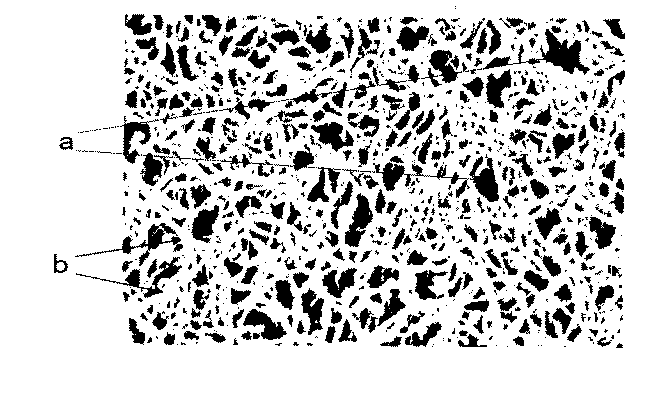
本樹脂板の制電層においては、炭素繊維が均一に分散しているので透明性、制電性が優れている。本発明において、炭素繊維が均一に分散しているとは、後述する手順1〜4により得られる画像の100μm×100μm辺りの輝度値129〜255の領域(図1のb部分、以後bともいう)の全面積が、輝度値0〜128の領域(図1のa部分、以後aともいう)の全面積とbの全面積との和の90%以下であり、かつbで囲まれたaの面積の最大値が0.3μm2以下であることをいう。 In the antistatic layer of the present resin plate, the carbon fibers are uniformly dispersed, so that the transparency and antistatic property are excellent. In the present invention, the carbon fibers are uniformly dispersed means a region of luminance values 129 to 255 around 100 μm × 100 μm of an image obtained by procedures 1 to 4 described later (b portion in FIG. 1, hereinafter also referred to as b). ) Is 90% or less of the sum of the total area of the regions having luminance values of 0 to 128 (part a in FIG. 1; hereinafter also referred to as a) and the total area of b, and a surrounded by b The maximum value of the area is 0.3 μm 2 or less.
本樹脂板の制電層上の後述する手順1〜4により得られる画像の100μm×100μm辺りのbの全面積の、aの全面積とbの全面積との和に対する面積比率の下限値は、40%以上、好ましくは45%以上、さらに好ましくは50%以上、上限値は90%以下、好ましくは80%以下、更に好ましくは70%以下である。制電層中の炭素繊維の面積比率が40%以上であれば、炭素繊維の面積比率が大きいので、炭素繊維同士の距離が長い箇所がないために、π電子がジャンプして導電性を示すトンネル効果が発生しやすく、トンネル電流を得られ導電性に劣るという問題が発生し難い。また、炭素繊維の占有率が90%以下では、可視光が透過し易く、透明性に優れる。 The lower limit of the area ratio with respect to the sum of the total area of a and the total area of b of the total area of b around 100 μm × 100 μm of the image obtained by steps 1 to 4 described later on the antistatic layer of the resin plate is 40% or more, preferably 45% or more, more preferably 50% or more, and the upper limit is 90% or less, preferably 80% or less, more preferably 70% or less. If the area ratio of the carbon fibers in the antistatic layer is 40% or more, the area ratio of the carbon fibers is large, and there is no place where the distance between the carbon fibers is long, so that π electrons jump and show conductivity. The tunnel effect is likely to occur, and the problem that the tunnel current can be obtained and the conductivity is poor is unlikely to occur. Further, when the occupation ratio of the carbon fibers is 90% or less, visible light is easily transmitted and the transparency is excellent.
本発明のbで囲まれたaの面積の最大値は、0.3μm2以下である。また、透明性、導電性の観点から、bの領域で囲まれたaの面積の最大値、0.3μm2以下、好ましくは0.2μm2以下、さらに好ましくは0.1μm2以下である。一方、bで囲まれたaの面積の最大値は、小さいほうが好ましいが、bで囲まれたaの面積の最大値が0.3μm2以下であれば、十分に制電性、透明性を発現することが可能である。 The maximum value of the area of a surrounded by b of the present invention is 0.3 μm 2 or less. From the viewpoint of transparency and conductivity, the maximum value of the area of a surrounded by the region b is 0.3 μm 2 or less, preferably 0.2 μm 2 or less, more preferably 0.1 μm 2 or less. On the other hand, the maximum value of the area of “a” surrounded by “b” is preferably small. However, if the maximum value of the area of “a” surrounded by “b” is 0.3 μm 2 or less, sufficient antistatic property and transparency can be obtained. It is possible to express.
本樹脂板の、100μm×100μm辺りのbの全面積の、aの全面積とbの全面積との和に対する面積比率と、bで囲まれたaの領域の面積の最大値は、本樹脂体の制電層の厚さを調節することにより、好ましい値に調整することが可能である。すなわち、本樹脂体の制電層の層厚が厚くすると、100μm×100μm辺りのbの全面積の、aの全面積とbの全面積との和に対する面積比率が高くなり、bで囲まれたaの面積の最大値は小さくなる。一方、制電層の厚さが薄くなると、100μm×100μm辺りのbの全面積の、aの全面積とbの全面積との和に対する面積比率が低くなり、bで囲まれたaの面積の最大値は大きくなる。 The area ratio of the total area of b of this resin plate around 100 μm × 100 μm to the sum of the total area of a and the total area of b and the maximum value of the area of the region a surrounded by b By adjusting the thickness of the body antistatic layer, it is possible to adjust to a preferable value. That is, when the thickness of the antistatic layer of this resin body is increased, the area ratio of the total area of b around 100 μm × 100 μm to the sum of the total area of a and the total area of b increases, and is surrounded by b. The maximum value of the area of a is small. On the other hand, when the thickness of the antistatic layer is reduced, the area ratio of the total area of b around 100 μm × 100 μm to the sum of the total area of a and the total area of b decreases, and the area of a surrounded by b The maximum value of becomes larger.
また、本樹脂板の100μm×100μm辺りのbの全面積の、aの全面積とbの全面積との和に対する面積比率と、bで囲まれたaの面積の最大値は、制電層中の炭素繊維の含有率を調節することによっても、好ましい値に調整することが可能である。すなわち、制電層の炭素繊維の含有率が多くなると、100μm×100μm辺りのbの全面積の、aの全面積とbの全面積との和に対する面積比率が高くなり、bで囲まれたaの面積の最大値は小さくなる。一方、制電層の炭素繊維の含有率が少なくなると、100μm×100μm辺りのbの全面積の、aの全面積とbの全面積との和に対する面積比率が低くなり、bで囲まれたaの面積の最大値は大きくなる。 In addition, the area ratio of the total area of b around 100 μm × 100 μm of this resin plate to the sum of the total area of a and the total area of b, and the maximum value of the area of a surrounded by b are the antistatic layer It can be adjusted to a preferable value by adjusting the content of the carbon fiber therein. That is, when the content of the carbon fiber in the antistatic layer increases, the area ratio of the total area of b around 100 μm × 100 μm to the sum of the total area of a and the total area of b increases, and is surrounded by b. The maximum value of the area of a becomes small. On the other hand, when the content ratio of the carbon fiber in the antistatic layer is reduced, the area ratio of the total area of b around 100 μm × 100 μm to the sum of the total area of a and the total area of b is reduced and surrounded by b The maximum value of the area of a is increased.
更に、本樹脂板の、100μm×100μm辺りのbの全面積の、aの全面積とbの全面積との和に対する面積比率と、bで囲まれたaの面積の最大値は、制電層中の炭素繊維の分散状態を調節することにより、好ましい値に調整することが可能である。すなわち、制電層中の炭素繊維の分散状態が良く、炭素繊維の凝集物無く分散している状態になると、100μm×100μm辺りのbの全面積の、aの全面積とbの全面積との和に対する面積比率が高くなり、bで囲まれたaの面積の最大値は小さくなる。一方、制電層中の炭素繊維の分散状態が良くなく、炭素繊維の凝集物が存在していると、100μm×100μm辺りのbの全面積の、aの全面積とbの全面積との和に対する面積比率が低くなり、bで囲まれたaの面積の最大値は大きくなる。 Furthermore, the area ratio of the total area of b of this resin plate around 100 μm × 100 μm to the sum of the total area of a and the total area of b, and the maximum value of the area of a surrounded by b are It is possible to adjust to a preferable value by adjusting the dispersion state of the carbon fibers in the layer. That is, when the dispersion state of the carbon fibers in the antistatic layer is good and the carbon fiber aggregates are dispersed, the total area of a and the total area of b of the total area of b around 100 μm × 100 μm The area ratio with respect to the sum of is increased, and the maximum value of the area of a surrounded by b is decreased. On the other hand, when the dispersion state of the carbon fibers in the antistatic layer is not good and the aggregates of the carbon fibers exist, the total area of a and the total area of b of the total area of b around 100 μm × 100 μm The area ratio with respect to the sum is reduced, and the maximum value of the area of a surrounded by b is increased.
制電層中の炭素繊維の分散状態を調節するには、分散方法、分散時間、分散剤の添加などを適宜選択することで、調整が可能となる。分散方法としては、公知の分散方法を使用することが可能であるが、ビーズミルによる炭素繊維を分散させることが好ましい。また、また分散時間は1時間行なうと通常炭素繊維の凝集物が少なくなった状態となる。また、添加する分散剤としては、例えば、ビス−2エチルへキシルスルホコハク酸塩、ドデシルスルホン産塩、アミン系分散剤、シランカップリング剤などがある。分散状態を調節するには、前記の分散方法の選択、分散時間の調節、分散剤の添加を単独で行なってもよいし、2種以上を組み合わせてもよい。例えば、分散方法としてはビーズミルを選択し、分散時間を1時間にすることで、良い分散状態を得ることができる。 In order to adjust the dispersion state of the carbon fibers in the antistatic layer, adjustment can be made by appropriately selecting a dispersion method, a dispersion time, addition of a dispersant, and the like. As a dispersion method, a known dispersion method can be used, but it is preferable to disperse carbon fibers by a bead mill. Further, when the dispersion time is performed for 1 hour, the carbon fiber aggregates are usually reduced. Examples of the dispersant to be added include bis-2-ethylhexylsulfosuccinate, dodecylsulfone salt, amine dispersant, and silane coupling agent. In order to adjust the dispersion state, the selection of the dispersion method, the adjustment of the dispersion time, and the addition of the dispersing agent may be carried out alone, or two or more kinds may be combined. For example, a good dispersion state can be obtained by selecting a bead mill as the dispersion method and setting the dispersion time to 1 hour.
(画像取得の手順及び画像処理の手順)
本発明の画像取得手順を以下に説明する。但し、本制電性樹脂板の画像取得方法は、以下に限定されない。すなわち、同様の条件、同様な画像が取得可能であれば公知の方法を採用することが可能である。また、画像処理手段とは、画像処理ソフトのことである。画像処理ソフトに関しては、バージョンアップされることがあるので、バージョンアップしたもので、本発明と同様な画像処理が可能であればバージョンアップしたものでの処理も可能とする。
(手順1:制電層表面のエッチング処理)
本樹脂板の制電層表面を下記条件1でイオンエッチング処理する。尚、イオンエチングとは、使用ガスになどを与え化し、プラズマ中のやが試料に衝突することを利用したエッチング方法である。尚本発明では、使用ガスとして空気を使用しているが、本樹脂板の制電層をイオンエッチングすることが可能であれば、公知の使用ガスを使用してもよい。例えば、アルゴンガス、窒素ガス等が挙げられる。使用ガスに空気を使用した場合には、空気中の主に窒素や酸素などがイオン化し制電層に衝突しスパッタリングが行なわれる。本発明では、放電電圧を200V、放電電流を20mA、処理時間を15分でイオンエッチング処理を行なったが、本発明の画像の取得が可能であれば、下記条件1より多少の変更があってもよい。
(条件1)
使用ガス:空気
放電電圧:200V(交流)
放電電流:20mA
時間 :15分間
(手順2:成膜処理)
スパッタリング装置(真空度8Pa)を用いて手順1で処理した制電層表面に膜厚5nmのPt−Pdをコートする。尚、Ptとは白金を意味し、Pbとは鉛を意味する。またPt−Pbの混合比率は、Pt:Pb=8:2のものを使用した。
(手順3:SEM観察による画像取得)
手順2で得られた試料より下記条件2でSEMを用いて画像を取得する。本発明でいう試料の傾斜角は、電子線照射方向に対して試料を傾斜させた角度をいう。また、ワーキングディスタンスとは、電子線レンズと試料との距離をいう。尚、ワーキングディスタンスの誤差範囲のずれは、本発明の得られる画像には、影響はほぼ無いと考えられる。
<条件2>
試料の傾斜角:30度
加速電圧:5kV
ワーキングディスタンス:15mm
直接倍率:30,000倍
(手順4:画像解析及び輝度値の面積測定)
手順3で得られた画像を下記条件3で画像処理手段を用いて解析し、得られた画像の輝度値0〜255の範囲におけるaの面積と、輝度値129〜255の領域の面積と、をそれぞれ測定する。尚、本発明の画像を取得することが可能であれば、他の画像処理手段(ソフト)を使用してもよい。
<条件3>
読み込み条件:8ビットグレースケール
明度:70
コントラスト:76
尚、この時にaと輝度値129〜255の領域を2値化して処理を行なってもよい。
(Image acquisition procedure and image processing procedure)
The image acquisition procedure of the present invention will be described below. However, the image acquisition method of the antistatic resin plate is not limited to the following. That is, a known method can be adopted as long as similar images and similar images can be acquired. The image processing means is image processing software. Since the image processing software may be upgraded, it can be upgraded, and if image processing similar to that of the present invention is possible, it can be processed with upgraded version.
(Procedure 1: Etching treatment on the surface of the antistatic layer)
The surface of the antistatic layer of the resin plate is subjected to ion etching treatment under the following condition 1. Note that ion etching is an etching method that utilizes the fact that gas in the plasma is applied to a sample and a sample in the plasma collides with a sample. In the present invention, air is used as the gas used, but a known gas used may be used as long as the antistatic layer of the resin plate can be ion-etched. For example, argon gas, nitrogen gas, etc. are mentioned. When air is used as the gas used, nitrogen or oxygen mainly in the air is ionized and collides with the antistatic layer to perform sputtering. In the present invention, the ion etching process was performed with a discharge voltage of 200 V, a discharge current of 20 mA, and a processing time of 15 minutes. However, if acquisition of the image of the present invention is possible, there are some changes from the following condition 1. Also good.
(Condition 1)
Gas used: Air discharge voltage: 200V (AC)
Discharge current: 20 mA
Time: 15 minutes (Procedure 2: Film formation process)
A surface of the antistatic layer treated in the procedure 1 is coated with Pt—Pd having a film thickness of 5 nm using a sputtering apparatus (vacuum degree: 8 Pa). Pt means platinum, and Pb means lead. The mixing ratio of Pt—Pb was Pt: Pb = 8: 2.
(Procedure 3: Image acquisition by SEM observation)
An image is acquired from the sample obtained in procedure 2 using SEM under the following condition 2. The inclination angle of the sample in the present invention refers to an angle at which the sample is inclined with respect to the electron beam irradiation direction. The working distance refers to the distance between the electron beam lens and the sample. Incidentally, it is considered that the deviation of the error range of the working distance has almost no influence on the image obtained by the present invention.
<Condition 2>
Sample tilt angle: 30 degrees Acceleration voltage: 5 kV
Working distance: 15mm
Direct magnification: 30,000 times (Procedure 4: Image analysis and luminance value area measurement)
The image obtained in the procedure 3 is analyzed using an image processing unit under the following condition 3, and the area of a in the range of luminance values 0 to 255 of the obtained image, the area of the region of luminance values 129 to 255, Measure each. Note that other image processing means (software) may be used as long as the image of the present invention can be acquired.
<Condition 3>
Reading condition: 8-bit gray scale Brightness: 70
Contrast: 76
At this time, the region of a and luminance values 129 to 255 may be binarized for processing.
(本樹脂板の製造方法)
本樹脂板は、一般的な方法により製造することが可能である。例えば、基材に直接塗布液をバーコータ、ロールコータ等で基材に塗布し制電層を設ける本樹脂板を製造する方法、転写法により基材に制電層を設けて本樹脂板を製造する方法等がある。本発明の制電性樹脂板を製造する塗布液は、溶剤、バインダー樹脂、炭素繊維、必要に応じて分散剤等の添加剤を溶剤に入れて攪拌し製造される。
(Production method of this resin plate)
The resin plate can be manufactured by a general method. For example, a method of manufacturing this resin plate in which a coating solution is directly applied to a substrate with a bar coater, roll coater, etc. to provide an antistatic layer, and an antistatic layer is provided on the substrate by a transfer method to produce this resin plate There are ways to do this. The coating liquid for producing the antistatic resin plate of the present invention is produced by adding a solvent, a binder resin, carbon fiber, and, if necessary, an additive such as a dispersant to the solvent and stirring.
(溶剤)
本樹脂板を製造する場合に使用する溶剤は、バインダー樹脂および炭素繊維の相溶性等を考慮し選択すれば良い。例えば、テトラヒドロフラン(THF)、シクロヘキサン、イソプロピルアルコールと水の混合溶液、エタノール、シクロヘキサンノンと酢酸エチルの混合溶液等が使用可能である。
(solvent)
The solvent used when producing the resin plate may be selected in consideration of the compatibility of the binder resin and the carbon fiber. For example, tetrahydrofuran (THF), cyclohexane, a mixed solution of isopropyl alcohol and water, ethanol, a mixed solution of cyclohexanenon and ethyl acetate, or the like can be used.
本樹脂板を製造する場合に用いる塗布液中おいて、炭素繊維が分散している状態にすることが好ましい。この炭素繊維が塗布液中で分散させる方法としては、公知の方法を使用することが可能である。例えば、塗布液中に分散剤を添加して、炭素繊維が分散している状態にしてもよいし、また塗布液を攪拌することにより、炭素繊維が分散している状態にしてもよい。 It is preferable that the carbon fibers are dispersed in the coating solution used for producing the resin plate. As a method of dispersing the carbon fiber in the coating solution, a known method can be used. For example, a dispersing agent may be added to the coating liquid so that the carbon fibers are dispersed, or the carbon fiber may be dispersed by stirring the coating liquid.
本樹脂板を製造する場合に用いる塗布液に添加する分散剤としては、具体的に酸性ポリマーのアルキルアンモニウム塩溶液や3級アミン修飾アクリル共重合物やポリオキシエチレン−ポリオキシプロピレン共重合物などの高分子系分散剤、カップリング剤等が使用される。分散剤の添加量は、炭素繊維の分散状態を確認しながら適当に調整することが好ましいが、例えば、制電層中の分散剤の添加量は、下限値が0.01質量%以上、好ましくは0.1質量%以上、さらに好ましくは0.5質量%以上であり、上限値が20質量%以下、好ましくは10質量%以下、さらに好ましくは5質量%以下である。分散剤の添加量が0.01質量%以上であれば炭素繊維を効率良く分散させることができ、20質量%以下であれば、制電層の導電性、透明性、強度を阻害することが無い。 Specific examples of the dispersant added to the coating solution used for producing the resin plate include an alkyl ammonium salt solution of an acidic polymer, a tertiary amine-modified acrylic copolymer, and a polyoxyethylene-polyoxypropylene copolymer. These polymer dispersants and coupling agents are used. The addition amount of the dispersant is preferably adjusted appropriately while confirming the dispersion state of the carbon fibers. For example, the addition amount of the dispersant in the antistatic layer has a lower limit of 0.01% by mass or more, preferably Is 0.1% by mass or more, more preferably 0.5% by mass or more, and the upper limit is 20% by mass or less, preferably 10% by mass or less, more preferably 5% by mass or less. If the addition amount of the dispersant is 0.01% by mass or more, the carbon fiber can be efficiently dispersed, and if it is 20% by mass or less, the conductivity, transparency and strength of the antistatic layer can be inhibited. No.
(分散方法)
本樹脂板を製造する場合に用いる塗布液を分散攪拌する方法としては、公知の方法が使用可能できる。例えば、攪拌羽根が高速で回転する際のせん断力により分散撹拌させる高速撹拌法、容器の中へビーズを充填しておき、中央の回転軸を回転させることにより、ビーズに動きを与え、ビーズ間で摺りつぶすビーズミル法、塗布液を高圧もしくは超高圧に加圧し、スリット(隙間)を抜ける際のせん断力を利用して分散撹拌させるホモジナイザー法、塗布液を、高速回転するホイールによって容器内壁に沿って薄膜状にして、容器内壁面との速度差により生ずる「ずり応力」によって、分散撹拌さ薄膜旋回法、塗布液同士を超高速で斜め衝突させて分散撹拌させる衝突法、超音波で真空の泡を発生させ、泡が潰れる力を使って分散撹拌させる超音波法などがある。
攪拌時間としては、攪拌方法にもよるが10分以上、好ましくは30分以上、さらに好ましくは60分以上行なえば炭素繊維が分散している塗布液を得ることが可能である。また、攪拌する時間は、5時間以内であれば、炭素繊維が切れずに、分散が良好な塗布液を得ることが可能である。
(Distribution method)
A known method can be used as a method for dispersing and stirring the coating solution used in the production of the resin plate. For example, a high-speed stirring method in which the stirring blades are dispersed and stirred by the shearing force when rotating at high speed, beads are filled in a container, and the central rotating shaft is rotated to give movement to the beads. The bead mill method that crushes the powder, the homogenizer method that pressurizes the coating solution to high pressure or ultra high pressure, and uses the shearing force when passing through the slit (gap) to stir and disperse the coating solution along the inner wall of the container with a wheel that rotates at high speed. The film is made into a thin film, and by the “shear stress” generated by the speed difference with the inner wall surface of the container, the dispersion stirring thin film swirl method, the collision method in which the coating liquids are obliquely collided with each other at high speed, the dispersion stirring is performed, There is an ultrasonic method in which bubbles are generated and dispersed and agitated using the force of crushing the bubbles.
Depending on the stirring method, the stirring time is 10 minutes or longer, preferably 30 minutes or longer, and more preferably 60 minutes or longer, whereby a coating liquid in which carbon fibers are dispersed can be obtained. Further, if the stirring time is within 5 hours, it is possible to obtain a coating solution with good dispersion without breaking the carbon fiber.
本樹脂板を製造するもう1つの例として、転写方法が挙げられる。すなわち、先ず、転写フィルム上に上記塗布液をバーコータ、ロールコータ等で塗布し、制電層を形成する。その後、熱可塑性樹脂の基板に、転写フィルム上に形成された制電層を基板に転写する方法がある。 Another example of manufacturing the resin plate is a transfer method. That is, first, the coating solution is applied onto a transfer film with a bar coater, a roll coater or the like to form an antistatic layer. Thereafter, there is a method in which the antistatic layer formed on the transfer film is transferred to the substrate of the thermoplastic resin.
本樹脂板を製造する更にもう1つの例として、先ず、基板とは異なるシートまたはフィルム上に上記塗布液をバーコータ、ロールコータ等で塗布し、制電層を形成する。その後、熱可塑性樹脂の基板と、制電層を形成したシートまたはフィルムを、基板とシートまたはフィルムが向き合うように配置し、熱プレス、熱加圧ロール等で熱融着させて制電層を基板上に形成する方法がある。 As yet another example of manufacturing the resin plate, first, the coating solution is applied on a sheet or film different from the substrate by a bar coater, a roll coater or the like to form an antistatic layer. After that, the thermoplastic resin substrate and the sheet or film on which the antistatic layer is formed are arranged so that the substrate and the sheet or film face each other, and the antistatic layer is formed by heat-sealing with a hot press, a hot press roll or the like. There is a method of forming on a substrate.
(基材)
本樹脂板を製造する場合に用いる基材は、公知の方法により製造することが可能である。例えば、押出し製造方法、押出し連続プレス方法、カレンダープレス製造方法等により製造可能である。また、市販されている樹脂板を購入してきて本樹脂板の基材とすることが可能である。
(Base material)
The base material used when manufacturing this resin board can be manufactured by a well-known method. For example, it can be manufactured by an extrusion manufacturing method, an extrusion continuous pressing method, a calendar press manufacturing method, or the like. In addition, a commercially available resin plate can be purchased and used as the base material of the resin plate.
(転写シート)
本樹脂板を製造する方法として、前記したように転写フィルムに形成された制電層を、樹脂成形体に転写する方法がある。本発明の転写フィルムは、転写基材と少なくとも一層の制電層を有する。必要に応じて、接着層を設けることもできる。
本発明で使用する転写基材は、制電層を構成する塗料に侵されないフィルムであれば限定されるものではないが、ポリエステル、ポリプロピレン、ポリエチレン、ポリカーボネート、ポリアミド、ポリイミド、ポリ塩化ビニル、ポリアクリレートなどの樹脂類、または金属箔などが適宜用いられる。中でも耐熱性、剛性の観点より、特に2軸延伸したポリエチレンテレフタレートが最も好ましく使用される。
(Transfer sheet)
As a method for producing the resin plate, there is a method of transferring the antistatic layer formed on the transfer film to the resin molded body as described above. The transfer film of the present invention has a transfer substrate and at least one antistatic layer. If necessary, an adhesive layer can be provided.
The transfer substrate used in the present invention is not limited as long as it is a film that is not affected by the paint constituting the antistatic layer, but polyester, polypropylene, polyethylene, polycarbonate, polyamide, polyimide, polyvinyl chloride, polyacrylate Resins such as these, or metal foils are used as appropriate. Of these, from the viewpoint of heat resistance and rigidity, biaxially stretched polyethylene terephthalate is most preferably used.
この転写基材の厚さの範囲は、下限値が10μm以上、好ましくは15μm以上、さらに好ましくは、30μm以上であり、上限値は200μm以下、好ましくは150μm以下、さらに好ましくは100μm以下である。転写基材の厚さが10μm以上であれば、転写フィルムの強度として好ましい、一方200μm以下であれば、転写の際の熱伝達性が良いという点で好ましい。
尚、本発明で使用する転写基材は、東レ株式会社(商品名:ルミラー)、東洋紡績株式会社(商品名:コスモシャイン)、三菱化学ポリエステル(商品名:ダイアホイルまたはフォスタファン)から商業的に入手可能である。
The range of the thickness of the transfer substrate is 10 μm or more, preferably 15 μm or more, more preferably 30 μm or more, and the upper limit is 200 μm or less, preferably 150 μm or less, more preferably 100 μm or less. If the thickness of the transfer substrate is 10 μm or more, it is preferable as the strength of the transfer film, while if it is 200 μm or less, it is preferable in terms of good heat transfer properties during transfer.
The transfer substrate used in the present invention is commercially available from Toray Industries, Inc. (trade name: Lumirror), Toyobo Co., Ltd. (trade name: Cosmo Shine), and Mitsubishi Chemical Polyester (trade name: Diafoil or Foster Fan). Is available.
以下、実施例について説明するが、本発明はこれに限定されるものではない。
(評価方法)
制電性樹脂板の制電層中の輝度値0〜128の領域および129〜255の領域の面積の測定
(1)制電性樹脂板の制電層表面のエッチング処理
日立ハイテクノロジーズ社製 Ion Sputter E−1030及びETCHING UNITを用い、以下の条件にて、本樹脂板の制電層にイオンエッチング処理を施し、制電層表面を処理した。
使用ガス:空気
放電電圧:200V(交流)
放電電流:20mA
時間 :15分間
(2)成膜処理
日立ハイテクノロジーズ社製 Ion Sputter E−1030を用い、イオンエッチング後の前記本樹脂板の制電層表面に、膜厚が5nmになるように、Pt−Pdを表面コートする。
(3)高分解能走査型電子顕微鏡(SEM)観察による画像の取り込み、日立ハイテクノロジーズ社製高分解能走査型電子顕微鏡(SEM)S−4500を用い、試料の傾斜角を30度、加速電圧5kV、ワーキングディスタンス15mm、直接倍率を30,000倍に設定し、画像を取得する。
(4)画像処理
得られた画像を、画像処理ソフト(Media Cybernetics,Inc.製 Image−Pro Plus Version4.0)を用い、8ビットグレースケールで取り込み、明度(0〜100)を70、コントラスト(0〜100)76に変換する。変換された画像の輝度値範囲0(暗)〜255(明)において、炭素繊維以外の領域画像の輝度値を0〜128、炭素繊維の領域画像の輝度値を129〜255として、各々の面積を測定した。面積比率を得るために、制電層の100μm×100μm辺りにおいて、輝度値129〜255の領域の全面積/(輝度値0〜128の領域の全面積と輝度値129〜255の領域の全面積との和)×100、により輝度値129〜255の領域の面積比率を算出する。尚前記「/」は、割り算を意味する。
2.表面抵抗率測定
制電性樹脂板の表面抵抗率はJIS K6911に準じて、以下のように行った。
(1)測定装置
ハイテスターUP MCP−HT450型 (三菱化学社製)
(2)測定方式
定電圧印加方式
(3)印加電圧
1000V
Hereinafter, although an example is described, the present invention is not limited to this.
(Evaluation methods)
Measurement of area of luminance value 0 to 128 and 129 to 255 in antistatic layer of antistatic resin plate (1) Etching treatment of antistatic layer surface of antistatic resin plate Ion made by Hitachi High-Technologies Corporation Using Sputter E-1030 and ETCHING UNIT, the antistatic layer of this resin plate was subjected to ion etching treatment under the following conditions to treat the antistatic layer surface.
Gas used: Air Discharge voltage: 200V (AC)
Discharge current: 20 mA
Time: 15 minutes (2) Film formation treatment Using Ion Sputter E-1030 manufactured by Hitachi High-Technologies Corporation, Pt-Pd so that the film thickness is 5 nm on the surface of the antistatic layer of the resin plate after ion etching. The surface is coated.
(3) Image capture by high-resolution scanning electron microscope (SEM) observation, using a high-resolution scanning electron microscope (SEM) S-4500 manufactured by Hitachi High-Technologies Corporation, the inclination angle of the sample is 30 degrees, the acceleration voltage is 5 kV, The working distance is set to 15 mm, the direct magnification is set to 30,000 times, and an image is acquired.
(4) Image Processing Using the image processing software (Image-Pro Plus Version 4.0, manufactured by Media Cybernetics, Inc.), the obtained image is captured in 8-bit gray scale, brightness (0-100) is set to 70, contrast ( 0-100) 76. In the luminance value range 0 (dark) to 255 (bright) of the converted image, the luminance value of the region image other than carbon fiber is 0 to 128, and the luminance value of the carbon fiber region image is 129 to 255. Was measured. In order to obtain the area ratio, in the area of 100 μm × 100 μm of the antistatic layer, the total area of the luminance values 129 to 255 / (the total area of the luminance values 0 to 128 and the total area of the luminance values 129 to 255) ) × 100, the area ratio of the region of luminance values 129 to 255 is calculated. The “/” means division.
2. Surface resistivity measurement The surface resistivity of the antistatic resin plate was measured as follows according to JIS K6911.
(1) Measuring device High Tester UP MCP-HT450 (Mitsubishi Chemical Corporation)
(2) Measurement method Constant voltage application method (3) Applied voltage 1000V
3.全光線透過率・ヘーズ値測定
制電性樹脂板の全光線透過率・ヘーズ値は、JIS K7105に準じて、以下の装置を使用して行った。
反射・透過率計:株式会社村上色彩技術研究所 HR−100
3. Measurement of total light transmittance / haze value The total light transmittance / haze value of the antistatic resin plate was measured using the following apparatus according to JIS K7105.
Reflectance / transmittance meter: Murakami Color Research Laboratory HR-100
(実施例、比較例)
THF(テトラヒドロフラン)溶剤に、下記に示すバインダー樹脂と炭素繊維(CNT社製 C100 繊維径10〜40nm、アスペクト比125〜2,000)とを表1の炭素繊維の割合になるように、塗料中で固形分(バインダー樹脂と炭素繊維の合計固形分)濃度が1.8質量%になるように添加し溶解・分散させ、塗料を作製した。
上記、塗料の中にガラスビーズ(アズワン社製 BZ−08)を塗料100質量部に対して、70質量部添加し、ペイントシェーカー(東洋精機製作所製)にて1時間撹拌させた。 撹拌後、塗料を濾過し、塗料とガラスビーズを分離した。
使用したバインダー樹脂:塩化ビニル樹脂(PVC:株式会社カネカ製 S−1008)、塩化ビニル−酢酸ビニル共重合体(塩ビ−酢ビ:新第一塩ビ株式会社製 C−150S 酢酸ビニル含有量11質量%)
(Examples and comparative examples)
In the paint so that the following binder resin and carbon fiber (C100 fiber diameter: 10 to 40 nm, aspect ratio: 125 to 2,000) manufactured by CNT may be mixed with the THF (tetrahydrofuran) solvent so as to have the carbon fiber ratio shown in Table 1. Then, the solid content (total solid content of binder resin and carbon fiber) was added so as to have a concentration of 1.8% by mass, and dissolved and dispersed to prepare a coating material.
Into the coating material, 70 parts by mass of glass beads (BZ-08 manufactured by ASONE Co., Ltd.) was added to 100 parts by mass of the coating material, and the mixture was stirred for 1 hour with a paint shaker (manufactured by Toyo Seiki Seisakusho). After stirring, the paint was filtered to separate the paint and glass beads.
Binder resin used: Vinyl chloride resin (PVC: S-1008 manufactured by Kaneka Corporation), vinyl chloride-vinyl acetate copolymer (vinyl chloride-vinyl acetate: manufactured by Shin-Daiichi PVC Co., Ltd.) C-150S Vinyl acetate content 11 mass %)
各塗料をポリエステルフィルム(三菱化学ポリエステルフィルム株式会社製 S100−50 厚み50μm ヘーズ値3.0%)にバーコータの番手を変えて制電層の厚みを表1のように調節して塗布し、100℃、3分で乾燥させ、ポリエステルフィルム上に制電層を形成した。 Each paint was applied to a polyester film (S100-50 manufactured by Mitsubishi Chemical Polyester Film Co., Ltd., thickness 50 μm, haze value 3.0%) by changing the number of the bar coater and adjusting the thickness of the antistatic layer as shown in Table 1. It was dried at 3 ° C. for 3 minutes to form an antistatic layer on the polyester film.
尚、制電層の厚みは、制電層/ポリエステルフィルムをミクロトームにて、それらの断面切片を作成し、走査型電子顕微鏡を用い観察した。 The thickness of the antistatic layer was observed using a scanning electron microscope by making a cross section of the antistatic layer / polyester film with a microtome.
前記、制電層/ポリエステルフィルムを、ポリエステルフィルム/制電層/塩化ビニル樹脂基板/制電層/ポリエステルフィルムの順に配置し、熱プレスにて制電層と塩化ビニル樹脂基板を一体化させた後、ポリエステルフィルムを剥離し、制電性樹脂板を作成した。
尚、用いた塩化ビニル樹脂基板は、厚み5mm(三菱樹脂社製ヒシプレート、ヘーズ値2.8%、全光線透過率72%、表面抵抗率2.2×10¹⁵Ω/□)、厚み20mm(三菱樹脂社製ヒシプレート、ヘーズ値3.2%、全光線透過率66%、表面抵抗率2.7×1015Ω/□)、厚み1mm(三菱樹脂社製ヒシプレート、ヘーズ値2.6%、全光線透過率80%、表面抵抗率3.9×1015Ω/□)のものを使用した。
また、熱プレスは、温度100℃、時間10分、圧力1.96MPaで行った。
The antistatic layer / polyester film was disposed in the order of polyester film / antistatic layer / vinyl chloride resin substrate / antistatic layer / polyester film, and the antistatic layer and the vinyl chloride resin substrate were integrated by hot pressing. Thereafter, the polyester film was peeled off to prepare an antistatic resin plate.
The vinyl chloride resin substrate used had a thickness of 5 mm (Hishi plate manufactured by Mitsubishi Plastics, haze value 2.8%, total light transmittance 72%, surface resistivity 2.2 × 10 15 Ω / □), thickness 20 mm. (Mitsubishi Resin Hishi Plate, haze value 3.2%, total light transmittance 66%, surface resistivity 2.7 × 10 15 Ω / □), thickness 1 mm (Mitsubishi Resin Hishi Plate, haze value 2. 6%, total light transmittance 80%, surface resistivity 3.9 × 10 15 Ω / □).
Moreover, the hot press was performed at a temperature of 100 ° C., a time of 10 minutes, and a pressure of 1.96 MPa.
得られた実施例1〜10、比較例1〜4、表面抵抗率、ヘーズ値、全光線透過率、輝度値129〜255の面積比率、輝度値0〜128の面積の最大値を表1に示した。尚、制電性樹脂板の制電層の厚みは、ミクロトームを用い、断面切片を作成し、走査型電子顕微鏡を用い観察した。 The obtained Examples 1 to 10, Comparative Examples 1 to 4, surface resistivity, haze value, total light transmittance, area ratio of luminance values 129 to 255, and maximum values of areas of luminance values 0 to 128 are shown in Table 1. Indicated. In addition, the thickness of the antistatic layer of the antistatic resin plate was observed using a microtome, creating a cross section and using a scanning electron microscope.
一方、比較例1、2は、前記した手順によって、走査型電子顕微鏡により得られた処理した画像において、輝度値0〜128の最大面積値が大きいので、炭素繊維の分散性に劣り、表面抵抗値が大きく、制電特性が十分に発現しなかった。 On the other hand, in Comparative Examples 1 and 2, in the processed image obtained by the scanning electron microscope according to the procedure described above, since the maximum area value of the luminance value 0 to 128 is large, the dispersibility of the carbon fiber is inferior and the surface resistance The value was large, and the antistatic characteristics were not sufficiently developed.
更に、比較例3、4は、前述した手順によって、走査型電子顕微鏡により得られた処理した画像において、輝度値129〜255面積比率が90以上であるために、透明性が悪かった。 Further, in Comparative Examples 3 and 4, the processed image obtained by the scanning electron microscope according to the above-described procedure had a luminance value of 129 to 255, and the area ratio was 90 or more, so the transparency was poor.
上述したように、本樹脂板は、透視性、導電性に優れ、特に量産性、経済性に優れた制電性樹脂板であり、クリーンルームのパーテーションや試験装置の覗き窓としての利用性が大きい。 As described above, this resin plate is an antistatic resin plate with excellent transparency and conductivity, particularly excellent in mass productivity and economy, and has a high utility as a viewing window for clean rooms and test equipment. .
a 輝度値0〜128の領域
b 輝度値129〜255の領域
a Area with luminance value 0 to 128 b Area with luminance value 129 to 255
Claims (4)
(手順1:制電層表面のエッチング処理)
制電層表面を下記条件1でイオンエッチング処理する。
<条件1>
使用ガス:空気
放電電圧:200V(交流)
放電電流:20mA
時間:15分間
(手順2:成膜処理)
スパッタリング装置(真空度8Pa)を用いて手順1で処理した制電層表面に膜厚5nmのPt−Pdをコートする。
(手順3:SEM観察による画像取得)
手順2で得られた試料より下記条件2でSEMを用いて画像を取得する。
<条件2>
試料の傾斜角:30度
加速電圧:5kV
ワーキングディスタンス:15mm
直接倍率:30,000倍
(手順4:画像解析及び輝度値の面積測定)
手順3で得られた画像を下記条件3で画像処理手段を用いて解析し、得られた画像の輝度値0〜255の範囲における輝度値0〜128の領域の面積と、輝度値129〜255の領域の面積と、をそれぞれ測定する。
<条件3>
読み込み条件:8ビットグレースケール
明度:70
コントラスト:76 An antistatic resin plate having a base material and at least one antistatic layer, wherein the antistatic layer contains carbon fiber, and has a luminance value of 129 to 255 around 100 μm × 100 μm of an image obtained by the following procedure. The total area of the region is 90% or less of the sum of the total area of the region with the luminance value of 0 to 128 and the total area of the region of the luminance value of 129 to 255, and is surrounded by the region with the luminance value of 129 to 255 The antistatic resin plate, wherein the maximum value of the area of the luminance value 0 to 128 is 0.3 μm 2 or less.
(Procedure 1: Etching treatment on the surface of the antistatic layer)
The surface of the antistatic layer is subjected to ion etching treatment under the following condition 1.
<Condition 1>
Gas used: Air Discharge voltage: 200V (AC)
Discharge current: 20 mA
Time: 15 minutes (Procedure 2: Film formation process)
A surface of the antistatic layer treated in the procedure 1 is coated with Pt—Pd having a film thickness of 5 nm using a sputtering apparatus (vacuum degree: 8 Pa).
(Procedure 3: Image acquisition by SEM observation)
An image is acquired from the sample obtained in procedure 2 using SEM under the following condition 2.
<Condition 2>
Sample tilt angle: 30 degrees Acceleration voltage: 5 kV
Working distance: 15mm
Direct magnification: 30,000 times (Procedure 4: Image analysis and luminance value area measurement)
The image obtained in the procedure 3 is analyzed using the image processing means under the following condition 3, and the area of the luminance value 0 to 128 in the range of the luminance value 0 to 255 of the obtained image and the luminance value 129 to 255 are obtained. The area of each area is measured.
<Condition 3>
Reading condition: 8-bit gray scale Brightness: 70
Contrast: 76
Priority Applications (1)
| Application Number | Priority Date | Filing Date | Title |
|---|---|---|---|
| JP2007266002A JP2009090611A (en) | 2007-10-12 | 2007-10-12 | Anti static resin plate, and transfer sheet for manufacturing anti static resin couple |
Applications Claiming Priority (1)
| Application Number | Priority Date | Filing Date | Title |
|---|---|---|---|
| JP2007266002A JP2009090611A (en) | 2007-10-12 | 2007-10-12 | Anti static resin plate, and transfer sheet for manufacturing anti static resin couple |
Publications (1)
| Publication Number | Publication Date |
|---|---|
| JP2009090611A true JP2009090611A (en) | 2009-04-30 |
Family
ID=40663076
Family Applications (1)
| Application Number | Title | Priority Date | Filing Date |
|---|---|---|---|
| JP2007266002A Pending JP2009090611A (en) | 2007-10-12 | 2007-10-12 | Anti static resin plate, and transfer sheet for manufacturing anti static resin couple |
Country Status (1)
| Country | Link |
|---|---|
| JP (1) | JP2009090611A (en) |
Cited By (1)
| Publication number | Priority date | Publication date | Assignee | Title |
|---|---|---|---|---|
| JP2015207003A (en) * | 2010-09-03 | 2015-11-19 | 日東電工株式会社 | Polarizing film, optical film laminate including polarizing film, and stretched laminate to be used for manufacturing optical film laminate including polarizing film |
-
2007
- 2007-10-12 JP JP2007266002A patent/JP2009090611A/en active Pending
Cited By (1)
| Publication number | Priority date | Publication date | Assignee | Title |
|---|---|---|---|---|
| JP2015207003A (en) * | 2010-09-03 | 2015-11-19 | 日東電工株式会社 | Polarizing film, optical film laminate including polarizing film, and stretched laminate to be used for manufacturing optical film laminate including polarizing film |
Similar Documents
| Publication | Publication Date | Title |
|---|---|---|
| TWI620802B (en) | Property enhancing fillers for transparent coatings and transparent conductive films | |
| EP1178075B1 (en) | Polyester film composite, light diffuser plate, and utilization thereof | |
| TWI545338B (en) | Anti-glare film, polarizing plate and image display device | |
| TWI517185B (en) | Transparent conductive laminates and transparent touch panels | |
| CN1543399A (en) | Coatings containing carbon nanotubes | |
| CN1745301A (en) | Articles with projected conductive coatings | |
| CN102763171A (en) | Low-haze transparent conductors | |
| CN1918005B (en) | Newton ring preventing sheet and touch panel using it | |
| WO2014050440A1 (en) | Transparent conductive laminate | |
| EP3594298A1 (en) | Method for producing silver nanowire ink, silver nanowire ink and transparent conductive coating film | |
| CN107210091A (en) | Transparent and electrically conductive film | |
| WO2016091104A1 (en) | Electrically conductive compositions, process and applications | |
| WO2019039209A1 (en) | Conductive paste, three-dimensional printed circuit, touch sensor, and methods respectively for producing those products | |
| Ding et al. | PC light-scattering material containing “pomegranate-like” SAN-SiO2 microspheres with excellent effective scattering range based the large-screen display | |
| TW201539482A (en) | Composition for forming transparent conductive layer | |
| JP2005290054A (en) | Additive for synthetic resin consisting of heavy calcium carbonate and synthetic resin composition containing the same | |
| JP2009090611A (en) | Anti static resin plate, and transfer sheet for manufacturing anti static resin couple | |
| JP5337500B2 (en) | Transparent conductive film and method for producing the same | |
| TW201920508A (en) | Method for producing conductive film, conductive film and metal nanowire ink | |
| Li et al. | Solvothermal synthesis of ultra-fine silver nanowires with a diameter about 20 nm and an aspect ratio approximately 2000 for highly conductive flexible transparent film | |
| Basri et al. | Quantitative analysis of MWCNT agglomeration in polymeric‐based membranes using atomic force microscope | |
| JP6896409B2 (en) | A sheet or film for a transparent screen, and a transparent screen equipped with the sheet or film. | |
| JP2010272514A (en) | Conductive oxide particulate dispersion composition, conductive paint composition, and conductive film | |
| WO2016129270A1 (en) | Electrode, method for producing same, and touch panel and organic el lighting element each provided with said electrode | |
| JP2009203282A (en) | Coating material for forming transparent antistatic film, transparent antistatic film using it, and transparent base material with transparent antistatic film |