JP2009089560A - Motor drive unit - Google Patents
Motor drive unit Download PDFInfo
- Publication number
- JP2009089560A JP2009089560A JP2007259233A JP2007259233A JP2009089560A JP 2009089560 A JP2009089560 A JP 2009089560A JP 2007259233 A JP2007259233 A JP 2007259233A JP 2007259233 A JP2007259233 A JP 2007259233A JP 2009089560 A JP2009089560 A JP 2009089560A
- Authority
- JP
- Japan
- Prior art keywords
- current
- motor
- circuit
- control
- constant current
- Prior art date
- Legal status (The legal status is an assumption and is not a legal conclusion. Google has not performed a legal analysis and makes no representation as to the accuracy of the status listed.)
- Withdrawn
Links
Images


Landscapes
- Control Of Stepping Motors (AREA)
Abstract
Description
本発明はモータ駆動装置、特にステッピングモータを低損失で振動・騒音を抑制しながら駆動するモータ駆動装置に関する。 The present invention relates to a motor drive device, and more particularly to a motor drive device that drives a stepping motor with low loss while suppressing vibration and noise.
複写機等における紙搬送用駆動源の位置決め制御に、ステッピングモータが利用されている。ステッピングモータは、フィードバックする必要が無いオープンループ制御で駆動することが可能なため多用されている。 A stepping motor is used for positioning control of a paper conveyance drive source in a copying machine or the like. Stepping motors are widely used because they can be driven by open loop control that does not require feedback.
そのステッピングモータの駆動方式としては、主に、
(1) 1相励磁方式、(2) 2相励磁方式、(3) 1−2相励磁方式、(4) uSTEP(マイクロステップ)駆動方式が知られている。
As a driving method of the stepping motor, mainly,
(1) One-phase excitation method, (2) Two-phase excitation method, (3) 1-2-phase excitation method, and (4) uSTEP (microstep) drive method are known.
また、利用用途に応じてステッピングモータの種類も使い分けられることが多く、その場合は下記のような選択となることが多い。
・PM(permanent magnet/永久磁石)型: 速度範囲が狭く、トルク範囲も大きくない用途
・ハイブリット型: 速度範囲が広く、トルク範囲も大きい用途
上記いずれのモータ構造を持つステッピングモータにおいても、モータ巻線のインダクタンス分による電流変化抑制と、駆動速度に応じた逆起電圧発生による電流入力制限が作用するため、モータの出力トルク特性は駆動範囲内で常に変化する。
In addition, the type of stepping motor is often used depending on the application, and in that case, the following selection is often made.
・ PM (permanent magnet) type: Applications that have a narrow speed range and a large torque range ・ Hybrid type: Applications that have a wide speed range and a large torque range Motor winding in any stepping motor with any of the above motor structures Since the current change suppression due to the inductance of the wire and the current input limitation due to the generation of the counter electromotive voltage according to the driving speed act, the output torque characteristic of the motor always changes within the driving range.
このような特性をもつステッピングモータにおいて、安定した出力トルクが得られる制御方法として、励磁する相(もしくは巻線)に流れる電流を一定とする定電流制御駆動回路が一般的に用いられている。 In a stepping motor having such characteristics, a constant current control drive circuit that makes a current flowing in an exciting phase (or winding) constant is generally used as a control method for obtaining a stable output torque.
この定電流制御方式の回路構成としては、一般的(たとえば非特許文献1参照)に、図15に示すように、相励磁パターン生成回路300と定電流制御回路202とで構成される。相励磁パターン生成回路300は、ステッピングモータの回転方向と回転速度に対応して入力された駆動パルス信号に従い上記(1)〜(3)に応じて各相(A,A*,B,B*)のオン/オフシーケンスを生成する。一方、定電流制御回路202は、オン/オフシーケンスにより規定された各相(A,A*,B,B*)のオン期間において、ステッピングモータの巻線電流を一定電流に制御する。
As a circuit configuration of this constant current control system, generally (for example, refer to Non-Patent Document 1), as shown in FIG. 15, a phase excitation
この定電流制御回路202では、ステッピングモータ100の各巻線LA/LA*/LB/LB*に流れる電流ia+ia*、ib+ib*を、電流検出回路203A/203Bで検出する。そして、各相の電流が規定の電流値となるように設定された電流設定回路201A/201Bと、電流検出部203A/203Bによる検出値とにより、PWM制御202A/202Bでオン・オフ比率を制御されたPWM信号が生成される。これらのPWM信号と前記励磁相信号A,A*,B,B*のそれぞれの論理積をとったものを、各巻線に接続された半導体スイッチング素子SW_A・SW_A*・SW_B・SW_B*の駆動信号とする。それで、所定の駆動期間内に流れる各巻線の電流をほぼ一定値となるように制御される。
In the constant
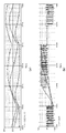
なお、(4)uSTEP駆動は、モータの構造により規定される基本ステップ角(2相:1.8度、5相:0.72度等)を、各巻線LA/LA*/LB/LB*の電流比率を制御することで、1/4,1/8...というように細分化を図る駆動方式である。1/4uSTEP時の各巻線の電流指令値を、図16に示す。図16に示すような電流指令値、を定電流駆動回路である図15の定電流指令値としてA相・B相に対して設定することで制御される。この電流比率は正弦関数から決定されており、細分化していくことで巻線に流れる電流波形は正弦波状に制御されることになる。 Note that (4) uSTEP drive uses a basic step angle (2 phases: 1.8 degrees, 5 phases: 0.72 degrees, etc.) defined by the motor structure for each winding LA / LA * / LB / LB *. By controlling the current ratio, the drive system is designed to be subdivided into 1/4, 1/8, and so on. FIG. 16 shows the current command value of each winding at ¼ uSTEP. Control is performed by setting the current command value as shown in FIG. 16 for the A phase and B phase as the constant current command value of FIG. 15 which is a constant current drive circuit. This current ratio is determined from a sine function, and by subdividing, the current waveform flowing in the winding is controlled in a sine wave shape.
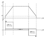
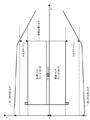
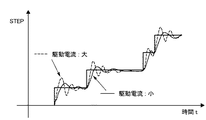
前述したようにステッピングモータはオープンループ制御で利用できる反面、モータの出力トルク以上の負荷変動が生じた場合には、脱調とよばれる指令値との同期はずれによるモータ停止状態になるという欠点も併せ持っている。これを回避するための一般的な手法として、例えば図13に示すように負荷をある加減速パターンで駆動する場合に必要なトルクに対して、モータ出力トルク範囲に図14のようにトルクマージン(通常必要トルクに対し1.5〜2倍)を設ける。つまり、脱調しないモータ出力トルクとなるように電流設定を行う。 As mentioned above, stepping motors can be used in open-loop control, but when load fluctuations exceed the motor output torque, the motor stops due to out-of-synchronization with a command value called step-out. Have both. As a general technique for avoiding this, for example, as shown in FIG. 13, the torque margin (as shown in FIG. 14) is included in the motor output torque range with respect to the torque required when the load is driven with a certain acceleration / deceleration pattern. Usually 1.5 to 2 times the required torque). That is, the current is set so that the motor output torque does not step out.
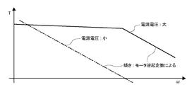
ここで、前述したモータ駆動速度により発生する逆起電圧要因でモータ巻線への電流制限が生じる領域は、図18に示すようにモータ出力トルクの傾きが大きくなる領域(以下定電圧駆動領域)となる。ここで分かるように、負荷駆動範囲がこの定電圧駆動領域にまで及ぶ場合には、駆動開始時を含む低速駆動領域におけるトルクマージンと、定電圧駆動領域でのトルクマージンとでは大きな差が生じることになる。結果として、このトルクマージンの大きさが駆動時に発生する振動を増加させることになるという欠点を備えている。 Here, the region where the current limit to the motor winding is caused by the counter electromotive voltage factor generated by the motor driving speed described above is a region where the inclination of the motor output torque becomes large as shown in FIG. 18 (hereinafter, constant voltage driving region). It becomes. As can be seen, when the load drive range extends to this constant voltage drive region, there is a large difference between the torque margin in the low speed drive region including the start of driving and the torque margin in the constant voltage drive region. become. As a result, the magnitude of this torque margin increases the vibration that occurs during driving.
つまり、駆動範囲が広い負荷を駆動する場合には、脱調防止を目的としてマージンを大きくすればするほど振動発生を助長することになる。この低速駆動領域におけるモータのステップ駆動動作による振動を抑制する手法としては、前述した駆動方式(4)のμSTEP駆動方式が有効な手段として一般的に利用されている。 That is, when driving a load having a wide driving range, the larger the margin is for the purpose of preventing step-out, the more the generation of vibration is promoted. As a method for suppressing vibration due to the step drive operation of the motor in this low speed drive region, the above-described μSTEP drive method of the drive method (4) is generally used as an effective means.
このuSTEP駆動によるモータ自身での低振動化は、
・駆動電流の正弦波化による発生トルクの高調波成分の低減
・基本ステップ角の分割
等によりなされる。
The vibration reduction by the motor itself by this uSTEP drive is
-Reduction of harmonic components of generated torque by sine wave of drive current-Division of basic step angle, etc.
ここで基本ステップ角の分割による、一般的に回転運動を行う物体に関する運動方程式は、加えるトルクをT[Nm]、トルクTの印加時間をt[s]、回転させる物体の慣性モーメントをJ[kgm2]、初期角速度をω0[rad/s]、変化後の角速度をω1[rad/s]とすると、
T=J*(ω1―ω0)/t ...(1)
で表され、その場合の運動エネルギーの変化量ΔKは
ΔK=J*(ω12―ω02)/2 ...(2)
ここで、角加速度ω'(=dω/dt)、変位角θとすると
(ω12―ω02)=2ω'θ ...(3)
であるから
ΔK=J*(ω12―ω02)/2=Tθ ...(4)
と表される。
Here, the equation of motion for an object that generally performs rotational motion by dividing the basic step angle is T [Nm] for the applied torque, t [s] for the application time of the torque T, and the inertia moment of the object to be rotated J [ kgm2], the initial angular velocity is ω0 [rad / s], and the angular velocity after the change is ω1 [rad / s]
T = J * (ω1-ω0) / t (1)
In this case, the kinetic energy variation ΔK is ΔK = J * (ω1 2 −ω0 2 ) / 2 (2)
Here, assuming that the angular acceleration ω ′ (= dω / dt) and the displacement angle θ, (ω1 2 −ω0 2 ) = 2ω′θ (3)
Therefore, ΔK = J * (ω1 2 −ω0 2 ) / 2 = Tθ (4)
It is expressed.
このように、角速度の変化量が大きくなる場合や駆動モータから負荷へ供給されるトルクが大きくなる場合に、運動エネルギーの変化量が大きくなり、結果として振動や騒音の増加を招くことになる。このため、角度の細分化によることで発生振動を抑制することが可能となる。 As described above, when the amount of change in angular velocity increases or when the torque supplied from the drive motor to the load increases, the amount of change in kinetic energy increases, resulting in an increase in vibration and noise. For this reason, it becomes possible to suppress the generated vibration by subdividing the angle.
ただし、基本ステップ角(電気角180度)毎にモータに入力されるエネルギーとしては、図17に示すように、フルステップ駆動時の矩形波電流に対し、低速領域(図17の(b))では正弦波電流となるため約1/√2程度へと減少する。また、高速領域では逆起電圧分の影響と、負荷角と呼ばれるモータ出力トルクと負荷トルクによる釣り合い角の影響により巻線電流量が変化が発生する。図17の(c)は、負荷トルクが比較的大きな値の場合の波形比較結果を示す。この場合でも、定電流制御値として、フルステップ駆動の矩形波指令値に対し、uSTEP駆動の正弦波指令値では、負荷角が大きくなり逆起電圧の発生位相が変化した場合でも巻線電流が抑制されてしまう。このため、約9割弱の値にしかならず、結果として図17の(a)のようにモータ出力トルクも減少する。 However, as shown in FIG. 17, the energy input to the motor at each basic step angle (electrical angle 180 degrees) is a low speed region ((b) in FIG. 17) with respect to a rectangular wave current during full step driving. Then, since it becomes a sine wave current, it decreases to about 1 / √2. Further, in the high-speed region, the winding current amount changes due to the influence of the counter electromotive voltage and the influence of the motor output torque called load angle and the balance angle of the load torque. FIG. 17C shows a waveform comparison result when the load torque is a relatively large value. Even in this case, as the constant current control value, the sine wave command value of the uSTEP drive with respect to the rectangular wave command value of the full-step drive, the winding current is increased even when the load angle becomes large and the back electromotive voltage generation phase changes. It will be suppressed. For this reason, the value is only about 90%, and as a result, the motor output torque is also reduced as shown in FIG.
つまり、同じモータ軸角速度で駆動する場合に、同じピーク電流設定値では、uSTEP駆動のほうがフルステップ駆動時に対し、振動は抑制される。しかし、トルクは減少方向となるため、より大きい電流設定とする必要性と電源電圧の高電圧化とが必要とされる。 That is, when driving at the same motor shaft angular velocity, vibration is suppressed in uSTEP driving compared to full step driving at the same peak current setting value. However, since the torque decreases, it is necessary to set a larger current and increase the power supply voltage.
これに関しては、分割数と駆動周波数に応じた電流制御値変更などのものが提案されている(特許文献1)。 In this regard, a method of changing the current control value according to the number of divisions and the driving frequency has been proposed (Patent Document 1).
また、低速領域での低振動化対策としては、駆動電流を最適な値とすることで、図19に示すように、ステップ動作時にロータの移動位置に対するオーバーシュート・アンダーシュートを少なくすることができる。これにより振動・騒音が低減できることが知られている。これをもとに、駆動電流を駆動周波数に応じて増減制御を行うもの等が提案されている(特許文献2)。
以上のようなステッピングモータ駆動時の問題点を改善し、かつ、駆動回路での損失低減を図る場合には、電源電圧を可変することが有効となる。 In order to improve the problems at the time of driving the stepping motor as described above and to reduce the loss in the drive circuit, it is effective to vary the power supply voltage.
しかし、電源電圧可変とする場合には昇圧、降圧構成のいずれの場合においても、インダクタンスL、コンデンサC、半導体スイッチ素子による回路構成と制御ICが必要となる。 However, when the power supply voltage is variable, a circuit configuration and a control IC using an inductance L, a capacitor C, and a semiconductor switch element are required in both cases of the step-up and step-down configurations.
また、さらに電圧レベルを任意可変制御とする場合には、どのタイミングで電圧レベルの変更を行うかを制御する要素が必要となるため、回路構成の複雑化を生じる欠点もあった。 Further, when the voltage level is arbitrarily variable controlled, an element for controlling at which timing the voltage level is changed is required, which causes a drawback in that the circuit configuration is complicated.
本発明は、上記従来の問題点に鑑み、回路および制御の簡略化を図ると共に、低振動で且つ低損失なモータ駆動装置を提供する。 In view of the above-described conventional problems, the present invention provides a motor driving device that simplifies the circuit and control, and has low vibration and low loss.
以上のような問題点に対し、本件では下記構成により回路・制御の簡略化を図り、低振動・低損失なモータ駆動装置を提案する。 In order to address the above problems, the present invention proposes a motor drive device with low vibration and low loss by simplifying the circuit and control with the following configuration.
すなわち、入力電圧をモータに供給するための電源回路と、前記モータに流れる電流を定電流値となるよう制御する定電流駆動回路とを有するモータ駆動装置において、前記定電流駆動回路が有する電流検出手段で検出された電流値と指令された定電流値とを比較して、比較結果に基づいて前記モータに流れる電流を制御する制御信号を発生する信号発生手段と、前記信号発生手段から発生した制御信号を受けて、前記制御信号に同期して前記入力電圧を変化させて前記モータに供給する可変電源回路とを有することを特徴とする。 That is, in a motor drive device having a power supply circuit for supplying an input voltage to a motor and a constant current drive circuit for controlling the current flowing through the motor to a constant current value, the current detection of the constant current drive circuit A signal generating means for comparing the current value detected by the means with the commanded constant current value and generating a control signal for controlling the current flowing through the motor based on the comparison result; and the signal generating means And a variable power supply circuit that receives the control signal, changes the input voltage in synchronization with the control signal, and supplies the input voltage to the motor.
ここで、前記可変電源回路は、前記制御信号に同期して前記入力電圧を昇圧して前記モータに供給する昇圧電源回路を含む。また、前記制御信号は、前記比較結果の電圧レベルでパルス幅変調されたパルス信号である。また、前記制御信号を遅延させて前記定電流駆動回路の制御を行なうマスク回路を更に有する。また、前記モータは、ステッピングであって、前記ステッピングモータの回転方向と回転速度を制御する信号を発生するための相励磁パターン生成回路を更に有する。また、前記可変電源回路を、前記ステッピングモータの各励磁相ごとに有する。また、前記相励磁パターン生成回路は、前記ステッピングモータの回転速度を示す定電流値を指令する電流指令手段を有する。 Here, the variable power supply circuit includes a boost power supply circuit that boosts the input voltage in synchronization with the control signal and supplies the boosted voltage to the motor. The control signal is a pulse signal that is pulse-width modulated with the voltage level of the comparison result. Further, it further includes a mask circuit for controlling the constant current drive circuit by delaying the control signal. The motor further includes a phase excitation pattern generation circuit for generating a signal for controlling a rotation direction and a rotation speed of the stepping motor. The variable power supply circuit is provided for each excitation phase of the stepping motor. The phase excitation pattern generation circuit has a current command means for commanding a constant current value indicating a rotation speed of the stepping motor.
また、本発明は、画像形成装置における負荷を駆動させるためのステッピングモータを駆動するモータ駆動装置であって、ステッピングモータの各相の巻線へ供給された電流を検出する電流検出手段と、前記電流検出手段により検出された巻線電流が所定の電流値となるように、電流値を指令するための電流指令手段と、前記電流検出手段により検出された巻線電流と前記電流指令手段により指令された電流値との差を検出するための比較手段と、前記比較手段により検出された巻線電流の差に応じて、前記各相の巻線へ供給される電流のオン/オフデューティ比を決定するPWM制御手段と、前記PWM制御手段から出力されるPWM信号に基づき、第1の半導体スイッチ素子をオン/オフ制御することで巻線電流を定電流制御する定電流制御手段と、前記定電流制御手段に直列に接続されたコイルおよび半導体整流素子と、前記コイルおよび半導体整流素子の間に並列に接続された第2の半導体スイッチ素子と、コンデンサとからなる電源供給手段とを有し、前記定電流制御を行うためのPWM制御手段により生成される前記PWM信号を、前記電源供給手段の第2の半導体スイッチ素子のオン/オフ制御を行う信号とし、前記電源供給手段の構成要素であるコイルおよびコンデンサにより決定される回路時定数を、前記ステッピングモータの巻線と第1の半導体スイッチ素子および回路抵抗の総和による抵抗分との回路時定数の1/2以下とすることを特徴とする。 The present invention also provides a motor driving device for driving a stepping motor for driving a load in the image forming apparatus, the current detecting means for detecting the current supplied to the winding of each phase of the stepping motor, A current command means for commanding a current value so that the winding current detected by the current detection means becomes a predetermined current value; a winding current detected by the current detection means; and a command by the current command means A comparison means for detecting a difference between the current value and the on / off duty ratio of the current supplied to the winding of each phase according to the difference in the winding current detected by the comparison means. A constant current control for controlling the winding current by controlling on / off of the first semiconductor switch element based on the PWM control means to be determined and the PWM signal output from the PWM control means Power supply comprising a control means, a coil and a semiconductor rectifier element connected in series to the constant current control means, a second semiconductor switch element connected in parallel between the coil and the semiconductor rectifier element, and a capacitor And the PWM signal generated by the PWM control means for performing the constant current control is a signal for performing on / off control of the second semiconductor switch element of the power supply means, and the power supply The circuit time constant determined by the coil and the capacitor which are constituent elements of the means is ½ or less of the circuit time constant of the resistance of the winding of the stepping motor and the sum of the first semiconductor switch element and the circuit resistance. It is characterized by doing.
ここで、前記PWM制御手段は、前記電流指令手段が指令した電流値と前記電流検出手段が検出した巻線電流の検出値とを前記比較手段により比較した結果の差に基づいて、前記PWM信号を最小のオフ期間で生成するよう制御し、前記定電流制御手段は、前記最小のオフ期間をマスクする手段を含んでスイッチング周期における100%の導通を可能とし、前記電源供給手段へ供給される前記PWM信号は、前記定電流制御手段における励磁相ごとに生成された前記PWM信号の論理和により生成される。また、前記電源供給手段は励磁相ごとに設けられ、それぞれの電源供給手段へ供給される前記PWM信号を、前記定電流制御手段における励磁相ごとの定電流制御のPWM信号とする。 Here, the PWM control means is configured to determine the PWM signal based on the difference between the current value commanded by the current command means and the detection value of the winding current detected by the current detection means by the comparison means. The constant current control means includes a means for masking the minimum off period, enables 100% conduction in a switching cycle, and is supplied to the power supply means. The PWM signal is generated by a logical sum of the PWM signals generated for each excitation phase in the constant current control means. The power supply means is provided for each excitation phase, and the PWM signal supplied to each power supply means is a constant current control PWM signal for each excitation phase in the constant current control means.
以上のような構成とすることで、回路および制御の簡略化を図ると共に、低振動で且つ低損失なモータ駆動装置を提供できる。 With the configuration as described above, a circuit and control can be simplified, and a motor drive device with low vibration and low loss can be provided.
すなわち、定電流駆動回路側で必要とする電流量に応じたデューティ比となるように生成されるPWM制御信号により、回転速度により発生する逆起電圧分を補正するように供給電圧レベルが制御される。これにより、低速領域では必要な電流制御量に応じて、電源電圧を低いレベルに制御することで、定電流制御回路、および、モータでの損失を低減する。かつ、高速領域では逆起電圧による電流抑制を緩和させるように作用することで、励磁切換時の電流立ち上がり時間の短縮、および、ステッピングモータ駆動回路の定電流制御範囲の拡大が可能となる。さらに、駆動装置全体としての省エネルギー化が図れる。 That is, the supply voltage level is controlled so as to correct the counter electromotive voltage generated by the rotational speed by the PWM control signal generated so as to have a duty ratio corresponding to the amount of current required on the constant current drive circuit side. The Thus, in the low speed region, the power supply voltage is controlled to a low level according to the required current control amount, thereby reducing the loss in the constant current control circuit and the motor. In addition, in the high-speed region, the current rise time at the time of excitation switching can be shortened and the constant current control range of the stepping motor drive circuit can be expanded by acting so as to reduce current suppression due to the back electromotive voltage. Furthermore, energy saving can be achieved as the entire drive device.
かかる本発明のモータ駆動装置を、帯電、露光、現像を繰り返して画像を形成するレーザープリンタやデジタル複写機などに利用する画像形成装置へ適用する。そして、紙搬送系における駆動モータによる振動抑制、また、カラー画像形成装置における各色(MYCK)毎の現像装置を回転体構造に内包して、色毎に回転させることで、複数色の現像を行う回転現像器の駆動モータにおける振動抑制を行う。その結果、機器駆動騒音を抑制し、かつ駆動源振動に起因する形成画像の劣化を防止できる。 The motor driving apparatus of the present invention is applied to an image forming apparatus used for a laser printer, a digital copying machine, or the like that forms an image by repeating charging, exposure, and development. Then, vibration suppression by a drive motor in the paper conveyance system, and development of each color (MYCK) in the color image forming apparatus is included in a rotating body structure, and a plurality of colors are developed by rotating for each color. Vibration suppression is performed in the drive motor of the rotary developer. As a result, device drive noise can be suppressed, and deterioration of the formed image due to drive source vibration can be prevented.
以下では、本発明の実施形態におけるモータ駆動装置について、図を参照しながら説明する。 Below, the motor drive device in embodiment of this invention is demonstrated, referring a figure.
<本発明のモータ駆動装置の概念>
まず、本発明のモータ駆動装置について、その理論的な説明を行なう。
<Concept of Motor Drive Device of the Present Invention>
First, the theoretical explanation is given about the motor drive device of the present invention.
(昇圧電源回路の例)
図1は、駆動回路への電源供給部となる昇圧電源回路のブロック図である。
(Example of step-up power supply circuit)
FIG. 1 is a block diagram of a step-up power supply circuit serving as a power supply unit to the drive circuit.
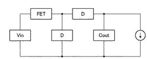
回路構成要素として、コイルL、半導体スイッチ素子としてのFET、ダイオードD、コンデンサCoutで構成される。 As circuit components, a coil L, an FET as a semiconductor switching element, a diode D, and a capacitor Cout are included.
図2に、図1の回路の動作状態を示す。 FIG. 2 shows the operating state of the circuit of FIG.
動作モードとしては次の2つがある。1つは、半導体スイッチ素子FETをオンして、コイルLに電流i1を供給し、エネルギーを蓄積するモード(a)である。もう1つは、前記FETをオフして、コイルLに蓄積されたエネルギーを入力電圧Vinに加算して、コンデンサCoutに対し電流i3として充電出力するモード(b)である。なお、接続された負荷(図には定電流源として示す)には両モード共に連続してコンデンサCoutから電力が供給される
この回路における入出力間の制御特性は、図2の(a)、(b)より次式で表される。
There are the following two operation modes. One is a mode (a) in which the semiconductor switch element FET is turned on, the current i1 is supplied to the coil L, and energy is accumulated. The other is a mode (b) in which the FET is turned off, the energy accumulated in the coil L is added to the input voltage Vin, and the capacitor Cout is charged and output as a current i3. The connected load (shown as a constant current source in the figure) is continuously supplied with power from the capacitor Cout in both modes. The control characteristics between the input and output in this circuit are shown in FIG. It is represented by the following formula from (b).
i1=i3
Vin/L×ton = (Vo−Vin)/L×toff
Vo=(ton+toff)/toff×Vin=1/(1−D)×Vin ...(5)
ここで、Tsw:スイッチング周期、D=ton/Tsw
つまり、スイッチオン期間tonが大きいほどインダクタLに蓄積されるエネルギーが増加して、出力電圧Voが大きくなる。
i1 = i3
Vin / L × ton = (Vo−Vin) / L × toff
Vo = (ton + toff) / toff * Vin = 1 / (1-D) * Vin (5)
Where Tsw: switching period, D = ton / Tsw
That is, as the switch-on period ton increases, the energy stored in the inductor L increases and the output voltage Vo increases.
(モータ側の定電流制御回路の例)
次に、モータ側の定電流制御回路のブロック図を、図3に示す。前述の昇圧回路と構成要素は同じである。異なる部分は半導体スイッチ素子FETの挿入位置関係とコイルL(これはモータ巻線に相当する)の位置関係のみである。
(Example of constant current control circuit on the motor side)
Next, a block diagram of a constant current control circuit on the motor side is shown in FIG. The components of the booster circuit are the same as those described above. The only difference is the insertion positional relationship of the semiconductor switch element FET and the positional relationship of the coil L (which corresponds to a motor winding).
図4に動作状態を示す。動作モードとしては次の2つがある。1つは、前記FETをオンしてコイルLに電流ic1を供給して、エネルギーを蓄積するモード(a)である。もう1つはと、前記FETをオフしてコイルLに蓄積されたエネルギーを負荷側へIc3として供給するモード(b)である。 FIG. 4 shows the operating state. There are the following two operation modes. One is a mode (a) in which the FET is turned on to supply a current ic1 to the coil L to accumulate energy. The other is mode (b) in which the FET is turned off and the energy stored in the coil L is supplied to the load side as Ic3.
この回路における入出力間の制御特性は、図4の(a)、(b)より次式であらわされる。 The control characteristic between the input and output in this circuit is expressed by the following equation from FIGS.
ic1=(Vin−Vo)/L×ton
ic3= Vo/L×toff
定電流制御は指令値Irefに基づき、上式で決定される電流となるようにオン/オフ制御が行われる。これを電圧の関係式とすると次式となる。
ic1 = (Vin−Vo) / L × ton
ic3 = Vo / L × toff
In the constant current control, on / off control is performed based on the command value Iref so that the current is determined by the above equation. If this is a relational expression of voltage, the following expression is obtained.
Vo=ton/(ton+toff)×Vin=D×Vin ...(6)
また、図5のように上記2つの回路ブロック動作を並記した場合、2つの回路ブロックの同期動作時において、エネルギー蓄積要素であるコイルLがそれぞれ異なるモードで動作することがわかる。
Vo = ton / (ton + toff) × Vin = D × Vin (6)
In addition, when the above-described two circuit block operations are written side by side as shown in FIG. 5, it can be seen that the coils L as energy storage elements operate in different modes when the two circuit blocks are synchronized.
つまり、前記(5)、(6)の2つの式と、図5で示される動作状態とから、定電流制御側の指令値に基づき電源供給部の動作指令を生成した場合に、定電流指令の定電流値の増減要求と電源出力の電圧値の増減要求が比例関係となり、制御可能となる。 That is, when the operation command of the power supply unit is generated based on the command value on the constant current control side from the two expressions (5) and (6) and the operation state shown in FIG. The constant current value increase / decrease request and the power output voltage value increase / decrease request are proportional to each other and can be controlled.
さて、実際のモータ巻線の定電流制御に対して、それを抑制する要素としては、巻線インダクタンスLmによる影響(電流変化抑制V/Lm・tonと、ωLの変化)と、モータ回転子の永久磁石による逆起電圧emとなる。 As a factor to suppress the constant current control of the actual motor winding, the influence of the winding inductance Lm (current change suppression V / Lm · ton and change in ωL), and the motor rotor The counter electromotive force em is generated by a permanent magnet.
Vin―em=Lm×dI/dt ...(7)
Vin=Lm×dI/dt+Ke×ω
ここで、Lm:巻線インダクタンス、Vin:電源電圧、dt:スイッチングON時間、em:モータ逆起電圧、ω:モータ軸速度、Ke:逆起定数
例えば、2相ステッピングモータのユニポーラ駆動の場合、図6に示すように各相電流はそれぞれ90度位相がずれた状態でパルス指令が入力される毎に励磁相がAB→A*B→A*B*→AB*等となるように切り替わる。しかし、励磁相がA→A*に切り替わる場合には、A相電流Imaは初期値0(正確には切換前のA*時に流れていた最終電流から0に戻って)から電流が流れ始める。
この場合定電流制御側ではデューティ最大で指令電流値になるまで動作するが、巻線に流れる電流Imaは巻線インダクタLmにより立ち上がり特性が規定されることになる。
Vin−em = Lm × dI / dt (7)
Vin = Lm × dI / dt + Ke × ω
Here, Lm: winding inductance, Vin: power supply voltage, dt: switching ON time, em: motor counter electromotive voltage, ω: motor shaft speed, Ke: counter electromotive constant For example, in the case of unipolar drive of a two-phase stepping motor, As shown in FIG. 6, each phase current is switched so that the excitation phase becomes AB → A * B → A * B * → AB * and so on each time a pulse command is input with the phase shifted by 90 degrees. However, when the excitation phase is switched from A to A *, the A-phase current Ima starts to flow from an initial value 0 (more precisely, it returns to 0 from the final current that flowed at A * before switching).
In this case, the constant current control side operates until the command current value reaches the maximum duty, but the rising current characteristic of the current Ima flowing through the winding is defined by the winding inductor Lm.
Ima=Vin/Lm×ton
一方、電流が指令値に追従した場合には、スイッチング時の電流変化幅dIは次式で表される。
Ima = Vin / Lm × ton
On the other hand, when the current follows the command value, the current change width dI during switching is expressed by the following equation.
dI=(Vin−Keω)/Lm×ton_sw ...(8)
dt=dI・Lm/(Vin−Keω)
これらの関係を図7に示す。図7は、巻線インダクタL=4[mH]、電源電圧:24[V]、逆起電圧定数:0.17[V・s/rad]とした場合のものである。
dI = (Vin−Keω) / Lm × ton_sw (8)
dt = dI · Lm / (Vin−Keω)
These relationships are shown in FIG. FIG. 7 shows the case where the winding inductor L = 4 [mH], the power supply voltage: 24 [V], and the counter electromotive voltage constant: 0.17 [V · s / rad].
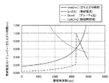
ここで、図7に示される各グラフに関して説明する。triseは駆動周波数(=回転数)に応じて増加する逆起電圧emにより、励磁切換時に定電流制御値に立ち上がるまでの時間と駆動周波数の関係を示す。Icntlは逆起電圧emと入力電圧Vinとの差電圧により、定電流制御される巻線電流と駆動周波数との関係を示す。図7のように、駆動速度が速くなると逆起電圧により定電流制御が行えなず定電圧制御(背景技術として説明した図18と同様)となることを示している。また、Dcnstは定電流制御時のデューティ比の変化を示すもので、前述の制御電流Icntlが逆起電圧の影響により定電流制御が行えなくなる領域ではデューティ比最大(=1=100%)となることを示す。t_plsは駆動周波数に応じた各相励磁時間幅を示したものである。 Here, each graph shown in FIG. 7 will be described. The rise represents the relationship between the drive frequency and the time required to rise to the constant current control value at the time of excitation switching due to the counter electromotive voltage em that increases with the drive frequency (= rotation speed). Icntl represents the relationship between the winding current and the drive frequency that are controlled by the constant current according to the difference voltage between the back electromotive force em and the input voltage Vin. As shown in FIG. 7, when the driving speed is increased, constant current control cannot be performed by the counter electromotive voltage, and constant voltage control (similar to FIG. 18 described as the background art) is performed. Dcnst indicates a change in duty ratio during constant current control, and the duty ratio becomes maximum (= 1 = 100%) in a region where the above-described control current Icntl cannot be controlled under the influence of the counter electromotive voltage. It shows that. t_pls indicates each phase excitation time width according to the drive frequency.
これらから、定電流制御指令値と電源供給部の制御指令値を共用した場合に、次のことが言える。
(1) 最大デューティで動作する期間は、励磁相切り替え時、および、定電圧領域(駆動パルス幅<電流立上がり時間)であり、負荷角変化(=逆起電圧位相変化)によるデューティ変化時
(2) 定電流領域で、定常状態の場合には、デューティは0.3以下であり、ホールド時などに励磁電流を減少させた場合には、さらにデューティ減少となるため、電源電圧増加率は小さくなる
<本実施形態のモータ駆動装置の構成例>
以下、本発明を適用した具体的な例を説明する。
From these, when the constant current control command value and the control command value of the power supply unit are shared, the following can be said.
(1) The period for operating at the maximum duty is when the excitation phase is switched, and in the constant voltage region (drive pulse width <current rise time), when the duty changes due to load angle change (= counter-electromotive voltage phase change) (2 ) In the constant current region, in the steady state, the duty is 0.3 or less, and when the excitation current is reduced during holding, the duty is further reduced, so the power supply voltage increase rate is reduced. <Example of Configuration of Motor Drive Device of Present Embodiment>
Hereinafter, specific examples to which the present invention is applied will be described.
図8に、可変電源回路211が、定電流制御用のパルス幅変調(以下、PWM)信号を電源供給部の電圧制御信号として共用する場合の回路ブロックを示す。ここでは、2相ステッピングモータ駆動回路として構成しており、A/B各相電流の制御信号の論理和をとって、電源制御用のPWM信号としている。かかる電源制御用のPWM信号は、可変電源回路211の第2の半導体スイッチ素子をオン/オフする。一方、定電流制御用のPWM信号は、ステッピングモータ駆動回路の第1の半導体スイッチ素子をオン/オフする。 FIG. 8 shows a circuit block when the variable power supply circuit 211 shares a pulse width modulation (hereinafter referred to as PWM) signal for constant current control as a voltage control signal for the power supply unit. Here, it is configured as a two-phase stepping motor drive circuit, and a logical sum of the control signals of the A / B phase currents is taken as a PWM signal for power supply control. The PWM signal for power supply control turns on / off the second semiconductor switch element of the variable power supply circuit 211. On the other hand, the PWM signal for constant current control turns on / off the first semiconductor switch element of the stepping motor drive circuit.
前述してきたように電源供給側のPWM信号は定電流制御側と同じように100%導通期間を設けると、インダクタの蓄積エネルギーが開放できない。ここでは、一般的なPWM制御ICとして各半導体メーカから供給されているTL494(TI製、そのほかNEC製uPC494等あり。内部回路ブロックを図9に示す)を用いた場合の構成として、次のようにした。
・ 定電流制御側にはCR積分回路からなるマスク回路204A/Bを設ける。
・ 電圧制御側にはマスク回路204A/B手前からの信号を利用する。
As described above, if the PWM signal on the power supply side is provided with a 100% conduction period as in the constant current control side, the stored energy of the inductor cannot be released. Here, as a configuration using a TL494 (manufactured by TI, others NEC uPC494, etc., the internal circuit block is shown in FIG. 9) supplied from each semiconductor manufacturer as a general PWM control IC, the following is provided. I made it.
A
-A signal from the front side of the
本発明の信号発生手段は、これらPWM制御回路202とマスク回路204を含むものである。
The signal generating means of the present invention includes these
これにより、図10に示すように、電圧制御側はPWM制御ICの最大オン/オフデューティ比(約90〜95%)での動作、定電流制御側は100%導通(最小オフ時間は増加する)として利用できる。 Thus, as shown in FIG. 10, the voltage control side operates at the maximum on / off duty ratio (about 90 to 95%) of the PWM control IC, and the constant current control side increases 100% conduction (the minimum off time increases). ).
なお、ここでは市販PWM制御ICを利用した場合について説明したが、回路をディスクリート構成とする場合でも、最小オフ幅が設けられる構成(例えば、図10の三角波の立ち下げ期間を必ずオフ幅とするなど)であれば何ら問題はない。 Although a case where a commercially available PWM control IC is used has been described here, a configuration in which a minimum off-width is provided even when the circuit has a discrete configuration (for example, the falling period of the triangular wave in FIG. 10 is always an off-width). Etc.) is no problem.
次に、回路定数に関して説明する。図1〜5で各回路ブロックの動作モードを示した。これら各回路ブロックはそれぞれ電源回路をLRC回路、モータ定電流制御回路をLR回路とおける。モータ定電流制御回路のLはステッピングモータの巻線、Rは半導体スイッチ素子と回路抵抗の総和の抵抗分である。これらの回路はいずれも回路定数による遅延要素を含んでいるため、電源回路時定数<モータ定電流回路時定数とする必要がある。ここでは、前述した励磁切換時に電源供給部での応答性を、PWM制御信号の最小オフ幅を含めて考慮し約1/2以下の時定数とする。 Next, circuit constants will be described. The operation mode of each circuit block is shown in FIGS. In each of these circuit blocks, the power circuit is an LRC circuit and the motor constant current control circuit is an LR circuit. In the motor constant current control circuit, L is the winding of the stepping motor, and R is the total resistance of the semiconductor switch element and the circuit resistance. Since these circuits all include delay elements due to circuit constants, it is necessary that power circuit time constant <motor constant current circuit time constant. Here, the response in the power supply unit at the time of the excitation switching described above is set to a time constant of about ½ or less in consideration of the minimum OFF width of the PWM control signal.
図8の回路において、モータ定電流制御回路の前段に半導体整流素子と直列に接続された可変電源回路211のコイルインダクタスLin、並列に接続された平滑コンデンサCinは一定とする。この時にモータ巻線インダクタンスLmを変化(□:0.5→◇:2→▽:5mH)させた場合の、電源電圧変化と巻線定電流動作波形をそれぞれ図11(a)、(b)に示す。このように、各回路間の時定数比が小さいと電源供給側の昇圧比が大きくなり必要範囲外での電圧上昇が増加することになり、スイッチング損失の増加を招くため、前述のように時定数の考慮が必要となる。 In the circuit of FIG. 8, the coil inductance Lin of the variable power supply circuit 211 connected in series with the semiconductor rectifier element and the smoothing capacitor Cin connected in parallel are set to be constant before the motor constant current control circuit. At this time, when the motor winding inductance Lm is changed (□: 0.5 → ◇: 2 → ▽: 5 mH), the power supply voltage change and the winding constant current operation waveform are shown in FIGS. 11A and 11B, respectively. Shown in As described above, if the time constant ratio between the circuits is small, the step-up ratio on the power supply side becomes large and the voltage rise outside the necessary range increases, resulting in an increase in switching loss. Consideration of constants is necessary.
以上のように、従来別々に構成されていた電源回路部と定電流回路部の制御系とを、定電流制御側を主制御の閉ループとして、それらを並列化ループとすることで、制御回路の省略および応答性の改善が図れる。 As described above, the control circuit of the power supply circuit unit and the constant current circuit unit, which have been conventionally configured separately, is set as a closed loop of the main control on the constant current control side, and these are made into parallel loops, thereby Omission and responsiveness can be improved.
また、図18の1点鎖線で示した電源電圧と逆起電圧によって決まる定電圧領域の範囲を、モータ側の必要トルクに応じて可変できる。そのため、各半導体スイッチ素子における損失は、同じスイッチング周期で電源出力レベル制御および定電流制御を行った場合に、電源電圧が低い方がオン期間でのFET等のスイッチング半導体素子におけるターンオンおよびターンオフ時のスイッチング損失を減少させられる。更に、オフ期間においても期間減少により回生電流経路でのダイオード(FETの寄生ダイオード含む)における損失も減少させることが可能となる。そのため、より低損失化が図れ、回路発熱による電解コンデンサなど熱による部品寿命への問題も抑制することが可能となる。 Further, the range of the constant voltage region determined by the power supply voltage and the back electromotive voltage indicated by the one-dot chain line in FIG. 18 can be varied according to the required torque on the motor side. Therefore, the loss in each semiconductor switching element is the same as when the power supply output level control and the constant current control are performed in the same switching cycle. Switching loss can be reduced. Further, even in the off period, the loss in the diode (including the parasitic diode of the FET) in the regenerative current path can be reduced by reducing the period. As a result, the loss can be further reduced, and the problem of the component life due to heat such as an electrolytic capacitor due to circuit heat generation can be suppressed.
<他の実施形態>
また、上記実施形態では、2相ステッピングモータにおいて、A相・B相での定電流制御PWM信号を併せて、電源供給部の電圧制御に利用している。しかし、図12に示すように、A相・B相のそれぞれに対して電源供給部を設ける構成とすることも可能である。この場合は、さらに、A/B相間での各相磁路のバラツキ分も補正される形で、それぞれの相が独立して制御可能となる。
<Other embodiments>
In the above embodiment, in the two-phase stepping motor, the constant current control PWM signals in the A phase and the B phase are also used for voltage control of the power supply unit. However, as shown in FIG. 12, it is also possible to employ a configuration in which a power supply unit is provided for each of the A phase and the B phase. In this case, each phase can be independently controlled in such a manner that the variation of each phase magnetic path between the A / B phases is also corrected.
つまり、相間での磁気抵抗差などにより発生するトルクリップルをも低減させることになるため、より低振動化が図れることになる。 That is, since the torque ripple generated due to the magnetoresistive difference between the phases is also reduced, the vibration can be further reduced.
Claims (10)
前記定電流駆動回路が有する電流検出手段で検出された電流値と指令された定電流値とを比較して、比較結果に基づいて前記モータに流れる電流を制御する制御信号を発生する信号発生手段と、
前記信号発生手段から発生した制御信号を受けて、前記制御信号に同期して前記入力電圧を変化させて前記モータに供給する可変電源回路とを有することを特徴とするモータ駆動装置。 In a motor drive device having a power supply circuit for supplying an input voltage to a motor and a constant current drive circuit for controlling a current flowing through the motor to have a constant current value,
Signal generating means for comparing the current value detected by the current detecting means of the constant current drive circuit with the commanded constant current value and generating a control signal for controlling the current flowing through the motor based on the comparison result When,
A motor drive apparatus comprising: a variable power supply circuit that receives a control signal generated from the signal generation means, changes the input voltage in synchronization with the control signal, and supplies the input voltage to the motor.
前記ステッピングモータの回転方向と回転速度を制御する信号を発生するための相励磁パターン生成回路を更に有することを特徴とする請求項1乃至4の何れか1項に記載のモータ駆動装置。 The motor is a stepping,
5. The motor driving apparatus according to claim 1, further comprising a phase excitation pattern generation circuit for generating a signal for controlling a rotation direction and a rotation speed of the stepping motor.
ステッピングモータの各相の巻線へ供給された電流を検出する電流検出手段と、
前記電流検出手段により検出された巻線電流が所定の電流値となるように、電流値を指令するための電流指令手段と、
前記電流検出手段により検出された巻線電流と前記電流指令手段により指令された電流値との差を検出するための比較手段と、
前記比較手段により検出された巻線電流の差に応じて、前記各相の巻線へ供給される電流のオン/オフデューティ比を決定するPWM制御手段と、
前記PWM制御手段から出力されるPWM信号に基づき、第1の半導体スイッチ素子をオン/オフ制御することで巻線電流を定電流制御する定電流制御手段と、
前記定電流制御手段に直列に接続されたコイルおよび半導体整流素子と、前記コイルおよび半導体整流素子の間に並列に接続された第2の半導体スイッチ素子と、コンデンサとからなる電源供給手段とを有し、
前記定電流制御を行うためのPWM制御手段により生成される前記PWM信号を、前記電源供給手段の第2の半導体スイッチ素子のオン/オフ制御を行う信号とし、
前記電源供給手段の構成要素であるコイルおよびコンデンサにより決定される回路時定数を、前記ステッピングモータの巻線と第1の半導体スイッチ素子および回路抵抗の総和による抵抗分との回路時定数の1/2以下とすることを特徴とするモータ駆動装置。 A motor driving device for driving a stepping motor for driving a load in an image forming apparatus,
Current detection means for detecting the current supplied to the winding of each phase of the stepping motor;
Current command means for commanding the current value so that the winding current detected by the current detection means has a predetermined current value;
Comparison means for detecting a difference between the winding current detected by the current detection means and the current value commanded by the current command means;
PWM control means for determining an on / off duty ratio of a current supplied to the windings of each phase according to a difference in winding current detected by the comparison means;
Constant current control means for performing constant current control of the winding current by controlling on / off of the first semiconductor switch element based on the PWM signal output from the PWM control means;
A power supply means comprising a coil and a semiconductor rectifying element connected in series to the constant current control means; a second semiconductor switching element connected in parallel between the coil and the semiconductor rectifying element; and a capacitor. And
The PWM signal generated by the PWM control means for performing the constant current control is a signal for performing on / off control of the second semiconductor switch element of the power supply means,
A circuit time constant determined by a coil and a capacitor which are constituent elements of the power supply means is 1 / of a circuit time constant of the winding of the stepping motor, the first semiconductor switch element, and a resistance component by the sum of circuit resistances. A motor drive device characterized by being 2 or less.
前記定電流制御手段は、前記最小のオフ期間をマスクする手段を含んでスイッチング周期における100%の導通を可能とし、
前記電源供給手段へ供給される前記PWM信号は、前記定電流制御手段における励磁相ごとに生成された前記PWM信号の論理和により生成されることを特徴とする請求項8に記載のモータ駆動装置。 The PWM control means is configured to reduce the PWM signal to a minimum based on a difference between the current value commanded by the current command means and the detection value of the winding current detected by the current detection means by the comparison means. Control to generate in the off period,
The constant current control means includes means for masking the minimum off period, and enables 100% conduction in a switching cycle;
9. The motor driving apparatus according to claim 8, wherein the PWM signal supplied to the power supply means is generated by a logical sum of the PWM signals generated for each excitation phase in the constant current control means. .
Priority Applications (1)
| Application Number | Priority Date | Filing Date | Title |
|---|---|---|---|
| JP2007259233A JP2009089560A (en) | 2007-10-02 | 2007-10-02 | Motor drive unit |
Applications Claiming Priority (1)
| Application Number | Priority Date | Filing Date | Title |
|---|---|---|---|
| JP2007259233A JP2009089560A (en) | 2007-10-02 | 2007-10-02 | Motor drive unit |
Publications (2)
| Publication Number | Publication Date |
|---|---|
| JP2009089560A true JP2009089560A (en) | 2009-04-23 |
| JP2009089560A5 JP2009089560A5 (en) | 2010-11-11 |
Family
ID=40662207
Family Applications (1)
| Application Number | Title | Priority Date | Filing Date |
|---|---|---|---|
| JP2007259233A Withdrawn JP2009089560A (en) | 2007-10-02 | 2007-10-02 | Motor drive unit |
Country Status (1)
| Country | Link |
|---|---|
| JP (1) | JP2009089560A (en) |
Cited By (3)
| Publication number | Priority date | Publication date | Assignee | Title |
|---|---|---|---|---|
| EP2530827A2 (en) | 2011-05-30 | 2012-12-05 | IAI Corporation | Control device, actuator system, and control method |
| CN107508512A (en) * | 2017-08-25 | 2017-12-22 | 深圳市泰奇科智能技术有限公司 | The Ultra-Low Speed prediction device control algolithm of closed loop stepper motor |
| CN111697887A (en) * | 2019-03-14 | 2020-09-22 | 罗姆股份有限公司 | Drive circuit for stepping motor, drive method for stepping motor, and electronic device using drive circuit |
-
2007
- 2007-10-02 JP JP2007259233A patent/JP2009089560A/en not_active Withdrawn
Cited By (5)
| Publication number | Priority date | Publication date | Assignee | Title |
|---|---|---|---|---|
| EP2530827A2 (en) | 2011-05-30 | 2012-12-05 | IAI Corporation | Control device, actuator system, and control method |
| CN107508512A (en) * | 2017-08-25 | 2017-12-22 | 深圳市泰奇科智能技术有限公司 | The Ultra-Low Speed prediction device control algolithm of closed loop stepper motor |
| CN107508512B (en) * | 2017-08-25 | 2020-01-31 | 深圳市泰奇科智能技术有限公司 | Ultra-low speed predictor control algorithm of closed-loop stepping motor |
| CN111697887A (en) * | 2019-03-14 | 2020-09-22 | 罗姆股份有限公司 | Drive circuit for stepping motor, drive method for stepping motor, and electronic device using drive circuit |
| CN111697887B (en) * | 2019-03-14 | 2024-02-13 | 罗姆股份有限公司 | Driving circuit of stepping motor, driving method thereof and electronic device using the same |
Similar Documents
| Publication | Publication Date | Title |
|---|---|---|
| Chang et al. | On the design of power circuit and control scheme for switched reluctance generator | |
| JP5740726B2 (en) | Method and hardware system for driving stepper motor in feedforward voltage mode | |
| US6806670B2 (en) | Energy converter control apparatus, and control method thereof | |
| US7518328B2 (en) | Method and device for commutating electromechanical actuators | |
| US7049786B1 (en) | Unipolar drive topology for permanent magnet brushless DC motors and switched reluctance motors | |
| KR20040010147A (en) | Control of a switched reluctance drive | |
| JP2011135775A (en) | Electronically-commutated type motor | |
| JP2002369568A (en) | Excitation of switched reluctance motor | |
| JP5770701B2 (en) | Stepping motor drive control device | |
| EP3121952A1 (en) | Method for operating a switched reluctance motor | |
| CN114503424A (en) | Drive circuit for stepping motor, drive method for stepping motor, and electronic device using the same | |
| JP2009089560A (en) | Motor drive unit | |
| JP2004208409A (en) | Power controller for vehicle | |
| JP2020150698A (en) | Driving circuit of stepping motor, driving method thereof, and electronic equipment using the same | |
| KR100976029B1 (en) | Ditc of srm drive system using 4-level converter | |
| US11264926B2 (en) | Driving circuit and method for stepping motor | |
| JP2008228477A (en) | Motor controller | |
| JP2022141750A (en) | Method for switching between block control method and pwm control method on electrical machine | |
| Ates et al. | Sliding mode control of a switched reluctance motor drive with four-switch Bi-Directional DC-DC converter for torque ripple minimization | |
| JP7199535B2 (en) | How to control a brushless permanent magnet motor | |
| CN111614290B (en) | Driving circuit of stepping motor, driving method thereof and electronic machine using same | |
| JP2010057256A (en) | Motor driving device | |
| JP5555954B2 (en) | Driving circuit | |
| JP4695924B2 (en) | Motor drive device | |
| JP2009065824A (en) | Controller for switched reluctance motor |
Legal Events
| Date | Code | Title | Description |
|---|---|---|---|
| A521 | Written amendment |
Free format text: JAPANESE INTERMEDIATE CODE: A523 Effective date: 20100928 |
|
| A621 | Written request for application examination |
Free format text: JAPANESE INTERMEDIATE CODE: A621 Effective date: 20100928 |
|
| A761 | Written withdrawal of application |
Free format text: JAPANESE INTERMEDIATE CODE: A761 Effective date: 20120208 |