JP2009076596A - Semiconductor device and manufacturing method thereof - Google Patents
Semiconductor device and manufacturing method thereof Download PDFInfo
- Publication number
- JP2009076596A JP2009076596A JP2007242768A JP2007242768A JP2009076596A JP 2009076596 A JP2009076596 A JP 2009076596A JP 2007242768 A JP2007242768 A JP 2007242768A JP 2007242768 A JP2007242768 A JP 2007242768A JP 2009076596 A JP2009076596 A JP 2009076596A
- Authority
- JP
- Japan
- Prior art keywords
- insulating film
- film
- adhesive layer
- phase change
- oxide
- Prior art date
- Legal status (The legal status is an assumption and is not a legal conclusion. Google has not performed a legal analysis and makes no representation as to the accuracy of the status listed.)
- Pending
Links
Images


Abstract
Description
本発明は、半導体装置およびその製造技術に関し、特に、不揮発性相変化メモリを備えた半導体装置に適用して有効な技術に関するものである。 The present invention relates to a semiconductor device and a manufacturing technique thereof, and more particularly to a technique effective when applied to a semiconductor device including a nonvolatile phase change memory.
近年、次世代不揮発性半導体メモリとして、カルコゲナイド(chalcogenide)のような相変化材料を用いた相変化メモリ(Phase-change Random Access Memory;PRAM)が提案されている。この相変化メモリは、不揮発性でありながら、書き込み・読出しの動作がDRAM(Dynamic Random Access Memory)と同程度に高速であると予想され、かつセル面積がフラッシュメモリと同程度に縮小可能であることから、次世代不揮発性メモリとして最有力視されている。 In recent years, a phase-change random access memory (PRAM) using a phase change material such as chalcogenide has been proposed as a next-generation nonvolatile semiconductor memory. Although this phase change memory is non-volatile, writing and reading operations are expected to be as fast as DRAM (Dynamic Random Access Memory), and the cell area can be reduced to the same extent as flash memory. Therefore, it is regarded as the most promising next-generation nonvolatile memory.
相変化メモリに用いられる相変化材料は、すでにDVD(Digital Versatile Disc)などの光ディスク媒体で使用されているが、DVDの場合は、相変化材料がアモルファス状態と結晶状態で光の反射率が異なる特性を利用している。例えば米国特許第5254382号(特許文献1)には、記録層として[(GeyTe1−y)a(SbzTe1−z)1−a]1−b(In1−xTex)b(ここで、0.4≦y≦0.6、0.3≦z≦0.6、0.4≦z≦0.6、0.1≦a≦0.5、0.01≦b≦0.3)で表される相変化材料を用いた光ディスク媒体が開示されている。これは、高速で結晶化が可能であるという特性を維持しつつ、非晶質状態の安定性を高め、データの長期保存性を向上することを目的として、Ge(ゲルマニウム)−Sb(アンチモン)−Te(テルル)にIn(インジウム)を添加したものである。 Phase change materials used for phase change memories are already used in optical disc media such as DVDs (Digital Versatile Discs). In the case of DVDs, the phase change materials have different light reflectivities depending on whether they are in an amorphous state or in a crystalline state. Utilizes characteristics. For example, in US Pat. No. 5,254,382 (Patent Document 1), [(Ge y Te 1-y ) a (Sb z Te 1-z ) 1-a ] 1-b (In 1-x Te x ) is used as a recording layer. b (where 0.4 ≦ y ≦ 0.6, 0.3 ≦ z ≦ 0.6, 0.4 ≦ z ≦ 0.6, 0.1 ≦ a ≦ 0.5, 0.01 ≦ b An optical disc medium using a phase change material represented by ≦ 0.3) is disclosed. The purpose of this is to improve the stability of the amorphous state and improve the long-term storage of data while maintaining the property that crystallization is possible at high speed. Ge (germanium) -Sb (antimony) -In (indium) added to Te (tellurium).
一方、相変化メモリの場合は、相変化材料がアモルファス状態と結晶状態で電気抵抗が数桁違う特性を利用し、メモリ素子として動作させるものである。相変化メモリのスイッチング、すなわち相変化材料のアモルファス状態から結晶状態への相変化およびその逆の変化は、相変化材料にパルス電圧を印加した際に発生するジュール熱を利用している。すなわち、アモルファス状態から結晶状態への相変化では、結晶化温度以上、融点以下となる電圧を印加し、結晶状態からアモルファス状態への相変化では、融点以上となる短パルスの電圧を加えて急冷する。 On the other hand, in the case of a phase change memory, the phase change material is operated as a memory element by utilizing the characteristic that the electric resistance is different by several orders of magnitude between the amorphous state and the crystalline state. The phase change memory switching, that is, the phase change from the amorphous state to the crystalline state of the phase change material and vice versa uses Joule heat generated when a pulse voltage is applied to the phase change material. That is, in the phase change from the amorphous state to the crystalline state, a voltage that is higher than the crystallization temperature and lower than the melting point is applied, and in the phase change from the crystalline state to the amorphous state, a short pulse voltage that is higher than the melting point is applied to rapidly cool. To do.
相変化メモリ用の相変化材料は、Ge2Sb2Te5を中心に研究が進められており、例えば特開2002−109797号公報(特許文献2)には、GeSbTeを用いた記録素子が開示されている。 Phase change materials for phase change memory have been studied mainly with Ge 2 Sb 2 Te 5. For example, Japanese Patent Application Laid-Open No. 2002-109797 (Patent Document 2) discloses a recording element using GeSbTe. Has been.
また、相変化メモリの一般的な構造については、「次世代光記録技術と材料」(エレクトロニクス材料・技術シリーズ、シーエムシー出版、2004年発行)(非特許文献1)の99頁、図6に記載がある。相変化メモリの場合、相変化膜と接する電極膜は、相変化膜のスイッチングの際に発生する熱に耐える必要があるため、この非特許文献1では、タングステンあるいはタングステンを含む合金が検討されている。また、低電流で相変化膜がスイッチングできるようにするために、下部電極は、相変化膜よりも面積の小さいプラグで構成されている。
For the general structure of phase change memory, see “Next Generation Optical Recording Technology and Materials” (Electronic Materials and Technology Series, CMC Publishing, 2004) (Non-Patent Document 1), page 99, FIG. There is a description. In the case of a phase change memory, the electrode film in contact with the phase change film needs to withstand the heat generated during switching of the phase change film. Therefore, in
一般に、上記したGeSbTeなどのカルコゲナイドは、層間絶縁膜材料である酸化シリコンとの密着性が悪いため、相変化メモリの製造時に相変化膜が層間絶縁膜から剥がれるという不具合が生じると、製造歩留まりの低下を引き起こす。そこで、相変化膜の剥がれを防止する方法として、相変化膜と層間絶縁膜との間に接着層を設ける構造が特開2003−174144号公報(特許文献3)や特開2006−352082号公報(特許文献4)で提案されている。 In general, chalcogenides such as GeSbTe described above have poor adhesion to silicon oxide, which is an interlayer insulating film material. Therefore, when a phase change film is peeled off from an interlayer insulating film during the manufacture of a phase change memory, the manufacturing yield is reduced. Causes a drop. Therefore, as a method for preventing the phase change film from peeling off, a structure in which an adhesive layer is provided between the phase change film and the interlayer insulating film is disclosed in Japanese Patent Laid-Open No. 2003-174144 (Patent Document 3) and Japanese Patent Laid-Open No. 2006-352082. (Patent Document 4).
特許文献3では、接着層としてTi(チタン)やドープトポリシリコンのような導電性材料を用いている。また、特許文献4では、接着層として、TiO(酸化チタン)、NbO(酸化ニオブ)、ZrO(酸化ジルコニウム)、HfO(酸化ハフニウム)、TaO(酸化タンタル)、CrO(酸化クロム)、MoO(酸化モリブデン)、WO(酸化タングステン)、AlO(酸化アルミニウム)のいずれかから選ばれた少なくとも一種以上の絶縁材料を用いている。
In
特開2006−351992号公報(特許文献5)に記載された相変化メモリは、プラグ状の第1電極と、第1電極上の相変化膜と、相変化膜上の第2電極とからなる抵抗素子を有し、上記第1電極に対向する部分の近傍の相変化膜および第2電極の断面形状を凸状または凹状とすることによって、第1電極の上端・外縁付近の電流集中を抑制している。
前述したように、相変化メモリにおいては、相変化膜と層間絶縁膜との剥がれを防止する方法として、特許文献3や特許文献4のように、相変化膜と層間絶縁膜との間に接着層を設けることが提案されている。
As described above, in the phase change memory, as a method for preventing peeling between the phase change film and the interlayer insulating film, as in
しかし、特許文献3のように、接着層を導電材料で構成した場合は、相変化メモリの書き換え時に接着層の面内を流れる電流が増加するために、書き換えに大きなエネルギーが必要になるという問題が生じる。一方、特許文献4のように、接着層を絶縁材料で構成した場合は、書き換え時に接着層の面内を大電流が流れることはない。
However, as in
しかし、特許文献4に記載された構造によれば、相変化メモリの下部電極を構成するプラグと相変化膜との界面全体に接着層が形成されているので、書き換え時には接着層にある程度の電流が流れる。このため、書き換えを繰り返すと、接着層に電流が繰返し流れることとなり、接着層を構成する金属原子あるいは酸素原子が相変化膜内に拡散し、相変化材料の電気抵抗率を変動させる場合があり、信頼性を損なう場合が発生する可能性がある。
However, according to the structure described in
本発明の目的は、相変化メモリの記憶層を構成する相変化膜と層間絶縁膜との剥がれを防止すると共に、層間絶縁膜と相変化膜との間に介在する接着層の構成原子が相変化膜内に拡散して相変化膜の特性を変動させる不具合を防止することにある。 An object of the present invention is to prevent peeling between the phase change film and the interlayer insulating film constituting the storage layer of the phase change memory, and the constituent atoms of the adhesive layer interposed between the interlayer insulating film and the phase change film are the phases. It is to prevent a problem that the characteristics of the phase change film are changed by diffusing into the change film.
本発明の前記ならびにその他の目的と新規な特徴は、本明細書の記述および添付図面から明らかになるであろう。 The above and other objects and novel features of the present invention will be apparent from the description of this specification and the accompanying drawings.
本願において開示される発明のうち、代表的なものの概要を簡単に説明すれば、次のとおりである。 Of the inventions disclosed in the present application, the outline of typical ones will be briefly described as follows.
本発明による半導体装置は、半導体基板の主面にトランジスタと相変化材料を含む抵抗素子とで構成された相変化メモリを備え、
前記抵抗素子は、前記トランジスタの上部に形成された層間絶縁膜内の導電性プラグからなる下部電極と、前記層間絶縁膜上に形成された絶縁材料からなる接着層と、前記接着層上に形成された前記相変化材料からなる記憶層と、前記記憶層上に形成された上部電極とを含んで構成され、
前記導電性プラグと前記記憶層は、少なくとも一部分が前記接着層を介することなく直接接しているものである。
A semiconductor device according to the present invention includes a phase change memory including a transistor and a resistance element including a phase change material on a main surface of a semiconductor substrate.
The resistance element is formed on the adhesive layer, a lower electrode made of a conductive plug in an interlayer insulating film formed on the transistor, an adhesive layer made of an insulating material formed on the interlayer insulating film, and A storage layer made of the phase change material formed, and an upper electrode formed on the storage layer,
At least a part of the conductive plug and the memory layer are in direct contact with each other without the adhesive layer.
本発明による半導体装置の製造方法は、半導体基板の主面にトランジスタと相変化材料を含む抵抗素子とで構成された相変化メモリを備えた半導体装置の製造方法であって、
(a)前記半導体基板の主面に前記トランジスタを形成する工程、
(b)前記トランジスタの上部に層間絶縁膜を形成した後、前記層間絶縁膜上に絶縁膜を形成する工程、
(c)前記絶縁膜および前記層間絶縁膜をエッチングして接続孔を形成した後、前記接続孔の内部に導電性プラグを形成し、前記トランジスタと前記導電性プラグとを電気的に接続する工程、
(d)前記絶縁膜および前記導電性プラグを覆うように、相変化材料からなる薄膜を形成した後、前記薄膜上に導電膜を形成する工程、
(e)前記導電膜および前記薄膜をパターニングすることにより、前記導電性プラグを下部電極とし、前記相変化材料からなる薄膜を記憶層とし、前記層間絶縁膜と前記記憶層との間に介在する前記絶縁膜を接着層とし、前記導電膜を上部電極とする前記抵抗素子を形成する工程を含んでいる。
A method for manufacturing a semiconductor device according to the present invention is a method for manufacturing a semiconductor device including a phase change memory including a transistor and a resistance element including a phase change material on a main surface of a semiconductor substrate,
(A) forming the transistor on a main surface of the semiconductor substrate;
(B) forming an insulating film on the interlayer insulating film after forming an interlayer insulating film on the transistor;
(C) a step of etching the insulating film and the interlayer insulating film to form a connection hole, and then forming a conductive plug in the connection hole to electrically connect the transistor and the conductive plug. ,
(D) forming a conductive film on the thin film after forming a thin film made of a phase change material so as to cover the insulating film and the conductive plug;
(E) By patterning the conductive film and the thin film, the conductive plug serves as a lower electrode, the thin film made of the phase change material serves as a memory layer, and is interposed between the interlayer insulating film and the memory layer. Forming the resistance element using the insulating film as an adhesive layer and the conductive film as an upper electrode.
本願において開示される発明のうち、代表的なものによって得られる効果を簡単に説明すれば以下のとおりである。 Among the inventions disclosed in the present application, effects obtained by typical ones will be briefly described as follows.
本発明によれば、記憶層と層間絶縁膜との界面に接着層を設けたことにより、記憶層と層間絶縁膜の剥離を防止することができる。また、層間絶縁膜上に接着層を設けたことにより、異種材料界面の数が増すので、界面熱抵抗が増加する。これにより、書き換え時にプラグ(下部電極)周辺の温度が上がり易くなるので、書き換えを低電力で行うことが可能となり、相変化メモリの低消費電力化を推進することができる。 According to the present invention, since the adhesive layer is provided at the interface between the memory layer and the interlayer insulating film, the memory layer and the interlayer insulating film can be prevented from being peeled off. Further, the provision of the adhesive layer on the interlayer insulating film increases the number of dissimilar material interfaces, thereby increasing the interface thermal resistance. As a result, the temperature around the plug (lower electrode) is likely to rise during rewriting, so that rewriting can be performed with low power, and low power consumption of the phase change memory can be promoted.
また、本発明によれば、プラグ(下部電極)と記憶層とが直接接しているので、書き換え時には接着層を介さずに電流を流すことができる。これにより、書き換えによる接着層構成原子の記憶層内への拡散を防止できるので、記憶層の電気抵抗率の経年変化が抑えられる。 Further, according to the present invention, since the plug (lower electrode) and the memory layer are in direct contact with each other, current can be passed through the adhesive layer without rewriting. Thereby, since the diffusion of the atoms constituting the adhesive layer into the memory layer due to rewriting can be prevented, the secular change of the electrical resistivity of the memory layer can be suppressed.
以下、本発明の実施の形態を図面に基づいて詳細に説明する。なお、実施の形態を説明するための全図において、同一の部材には原則として同一の符号を付し、その繰り返しの説明は省略する。 Hereinafter, embodiments of the present invention will be described in detail with reference to the drawings. Note that components having the same function are denoted by the same reference symbols throughout the drawings for describing the embodiment, and the repetitive description thereof will be omitted.
図1は、本発明の一実施の形態である半導体装置のメモリアレイ構成を示す要部回路図である。なお、図1は、説明が煩雑になるのを防ぐために、メモリアレイの一部(4本のワード線WL1〜WL4および4本のビット線BL1〜BL4)を示すに留めている。 FIG. 1 is a principal circuit diagram showing a memory array configuration of a semiconductor device according to an embodiment of the present invention. Note that FIG. 1 shows only a part of the memory array (four word lines WL1 to WL4 and four bit lines BL1 to BL4) in order to prevent the explanation from becoming complicated.
ワード線WL1には、4つのメモリセル(MC11〜MC14)が接続されている。同様に、ワード線WL2〜WL4のそれぞれには、メモリセルMC21〜MC24、MC31〜MC34、MC41〜MC44が接続されている。ワード線WL1〜WL4を駆動するのは、ワードドライバWD1〜WD4である。ワードドライバWD1〜WD4のいずれを選択するかは、ロウデコーダ(Xアドレスデコーダ)XDECからの信号により決まる。一方、ビット線BL1には、4つのメモリセル(MC11〜MC41)が接続されている。同様に、ビット線BL2、BL3、BL4のそれぞれには、メモリセルMC12〜MC42、MC13〜MC43、MC14〜MC44が接続されている。 Four memory cells (MC11 to MC14) are connected to the word line WL1. Similarly, memory cells MC21 to MC24, MC31 to MC34, and MC41 to MC44 are connected to the word lines WL2 to WL4, respectively. The word drivers WL1 to WD4 drive the word lines WL1 to WL4. Which one of the word drivers WD1 to WD4 is selected is determined by a signal from a row decoder (X address decoder) XDEC. On the other hand, four memory cells (MC11 to MC41) are connected to the bit line BL1. Similarly, memory cells MC12 to MC42, MC13 to MC43, and MC14 to MC44 are connected to the bit lines BL2, BL3, and BL4, respectively.
ビット線BL1〜BL4のそれぞれは、メモリアレイの外周に配置された選択トランジスタQD1〜QD4のソース側に接続される。選択トランジスタQD1、QD2は、互いのドレイン領域を共有し、選択トランジスタQD3、QD4は、互いのドレイン領域を共有している。これらの選択トランジスタ(QD1〜QD4)は、各ビット線(BL1〜BL4)のプリチャージを行う機能を持つ。また、ビットデコーダYDEC1あるいはビットデコーダYDEC2からの信号を受けて所定のビット線BLを選択する働きも持つ。この例では、ビットデコーダYDEC1とビットデコーダYDEC2は、ビット線2本置きに、選択するビット線BLを交互に受け持つ。読み出しによる出力は、センスアンプSAにより検出される。 Each of bit lines BL1 to BL4 is connected to the source side of select transistors QD1 to QD4 arranged on the outer periphery of the memory array. The selection transistors QD1 and QD2 share a drain region with each other, and the selection transistors QD3 and QD4 share a drain region with each other. These selection transistors (QD1 to QD4) have a function of precharging the bit lines (BL1 to BL4). Also, it has a function of receiving a signal from the bit decoder YDEC1 or the bit decoder YDEC2 and selecting a predetermined bit line BL. In this example, the bit decoder YDEC1 and the bit decoder YDEC2 alternately handle the selected bit line BL every two bit lines. The output by reading is detected by the sense amplifier SA.
上記メモリセル(MC11〜MC44)のそれぞれは、1個のnチャネル型MOSトランジスタからなるメモリセルトランジスタQMと、このメモリセルトランジスタQMに直列に接続された1個の抵抗素子RMとによって構成されている。メモリセルトランジスタQMのゲート電極にはワード線WLが接続されており、抵抗素子RMの一方の電極にはビット線BLが接続されている。 Each of the memory cells (MC11 to MC44) is composed of a memory cell transistor QM composed of one n-channel MOS transistor and one resistance element RM connected in series to the memory cell transistor QM. Yes. A word line WL is connected to the gate electrode of the memory cell transistor QM, and a bit line BL is connected to one electrode of the resistance element RM.
メモリアレイ以外の回路ブロックを構成する半導体素子は、特に限定されないが、典型的にはCMOS(Complementary MOS、相補型MOSトランジスタ)トランジスタからなり、公知のLSI製造技術によって、半導体基板(チップ)上に形成される。 The semiconductor elements constituting the circuit blocks other than the memory array are not particularly limited, but typically include CMOS (Complementary MOS, complementary MOS transistors) transistors, which are formed on a semiconductor substrate (chip) by a known LSI manufacturing technique. It is formed.
図中の符号VPLは各ワードドライバWDへの電源供給線、Vddは電源電圧である。VGLは各ワードドライバーWDの電位引抜き線であり、ここでは接地電位に固定されている。SLはソース線である。 In the figure, VPL is a power supply line to each word driver WD, and Vdd is a power supply voltage. VGL is a potential lead line of each word driver WD, and is fixed to the ground potential here. SL is a source line.
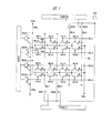
次に、本実施の形態のメモリセルの具体的な構成を図2を用いて説明する。同図は、図1に示したメモリアレイの一部(メモリセルMC11、MC21)を示す半導体基板の要部断面図である。 Next, a specific structure of the memory cell of this embodiment will be described with reference to FIG. This figure is a fragmentary cross-sectional view of a semiconductor substrate showing a part of the memory array (memory cells MC11, MC21) shown in FIG.
メモリセルMC11は、メモリセルトランジスタQM1と抵抗素子RM1とで構成され、メモリセルMC21は、メモリセルトランジスタQM2と抵抗素子RM2とで構成されている。メモリセルトランジスタQM1、QM2のそれぞれは、例えばp型単結晶シリコンからなる半導体基板1のp型ウエル2に形成されたnチャネル型MOSトランジスタであり、ゲート絶縁膜3とゲート電極4とLDD(Lightly Doped Drain)構造のn型半導体領域(ソース、ドレイン)6とを有している。n型半導体領域6の一方(ソース)は、2個のメモリセルトランジスタQM1、QM2によって共有されている。メモリセルトランジスタQM1、QM2は、半導体基板1に形成された素子分離溝9によって隣接メモリセルと分離されている。
The memory cell MC11 includes a memory cell transistor QM1 and a resistance element RM1, and the memory cell MC21 includes a memory cell transistor QM2 and a resistance element RM2. Each of the memory cell transistors QM1 and QM2 is an n-channel MOS transistor formed in a p-type well 2 of a
メモリセルトランジスタQM1のゲート電極4は、ワード線WL1を構成し、メモリセルトランジスタQM2のゲート電極4は、ワード線WL2を構成している。ゲート電極4(ワード線WL1、WL2)の表面にはCoシリサイド層7が形成されており、側壁にはサイドウォールスペーサ8が形成されている。また、n型半導体領域(ソース、ドレイン)6の表面には、Coシリサイド層7が形成されている。
The
メモリセルトランジスタQM1、QM2の上部には、層間絶縁膜10が形成されており、その上面は、半導体基板1の全面で高さがほぼ一致するように平坦化されている。層間絶縁膜10には、メモリセルトランジスタQM1、QM2のn型半導体領域(ソース、ドレイン)6の表面を露出する接続孔11、12が形成されており、それらの内部には、Coシリサイド層7に接続されたプラグ13が埋め込まれている。
An interlayer insulating
層間絶縁膜10の上部には、層間絶縁膜14が形成されている。この層間絶縁膜14には、配線溝15、16が形成されており、それらの内部には、第1層配線17、18が形成されている。配線溝16の内部に形成された第1層配線18は、接続孔12の内部のプラグ13を介してメモリセルトランジスタQM1、QM2のn型半導体領域(ドレイン)6に接続されており、配線溝15の内部に形成された第1層配線17は、接続孔11の内部のプラグ13を介して、メモリセルトランジスタQM1、QM2に共通のn型半導体領域(ソース)6に接続されている。この第1層配線17は、図1に示したソース線SLに相当する。
An interlayer insulating
層間絶縁膜14の上部には、層間絶縁膜20が形成されている。この層間絶縁膜20には、第1層配線18を露出する接続孔21、22が形成されており、それらの内部にはプラグ23が埋め込まれている。接続孔21の内部のプラグ23は、後述する抵抗素子RM1の下部電極を構成しており、第1層配線18およびその下部のプラグ13を介してメモリセルトランジスタQM1のn型半導体領域(ドレイン)6に接続されている。また、接続孔22の内部のプラグ23は、抵抗素子RM2の下部電極を構成しており、第1層配線18およびその下部のプラグ13を介してメモリセルトランジスタQM2のn型半導体領域(ドレイン)6に接続されている。
An interlayer insulating
層間絶縁膜20上には抵抗素子RM1、RM2が形成されている。抵抗素子RM1、RM2のそれぞれは、プラグ23(下部電極)と、その上部に積層された接着層24、記憶層25および上部電極26によって構成されており、上部電極26の上部には、キャップ絶縁膜27が形成されている。接着層24は、記憶層25と層間絶縁膜20との界面剥離を防止するために設けられているが、本実施の形態では、プラグ23(下部電極)の上面には、接着層24が設けられていない。
Resistive elements RM1 and RM2 are formed on the
抵抗素子RM1、RM2の上部には、層間絶縁膜28が形成されている。この層間絶縁膜28およびキャップ絶縁膜27には、抵抗素子RM1、RM2の上部電極26を露出する接続孔30、31が形成されており、それらの内部にはプラグ32が埋め込まれている。
An interlayer insulating
層間絶縁膜28の上部には、第2層配線33が形成されている。この第2層配線33は、図1に示したビット線BL1に相当する。第2層配線33(ビット線BL1)は、接続孔30、31の内部のプラグ32を介して、抵抗素子RM1、RM2の上部電極26に接続されている。なお、第2層配線33の上部には、層間絶縁膜が形成されているが、その図示は省略する。また、この層間絶縁膜のさらに上部には、必要に応じて第3層配線が形成されることもある。
A
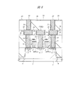
次に、図2に示したメモリセルの製造方法の一例を図3〜図8を用いて工程順に説明する。 Next, an example of a method for manufacturing the memory cell shown in FIG. 2 will be described in the order of steps with reference to FIGS.
まず、図3に示すように、p型の単結晶シリコンからなる半導体基板1を用意し、その主面に公知の方法を用いてp型ウエル2および素子分離溝9を形成する。次に、p型ウエル2にメモリセルトランジスタQM1、QM2を形成する。
First, as shown in FIG. 3, a
メモリセルトランジスタQM1、QM2を形成するには、まず、p型ウエル2の表面を熱処理および窒化処理することにより、酸窒化シリコン膜からなる膜厚1.5〜10nm程度のゲート絶縁膜3を形成する。続いて、半導体基板1上にCVD法で膜厚150〜200nm程度のn型多結晶シリコン膜を堆積した後、この多結晶シリコン膜をドライエッチングすることによって、ゲート電極4(ワード線WL1、WL2)を形成する。ゲート電極4(ワード線WL1、WL2)は、例えば多結晶シリコン膜とWシリサイド膜との積層膜で代替することもできる。
In order to form the memory cell transistors QM1 and QM2, first, the surface of the p-
次に、p型ウエル2にP(リン)をイオン注入することによって、ゲート電極4の両側壁の下部にn−型半導体領域(符号省略)を形成する。続いて、半導体基板1上にCVD法で酸化シリコン膜を堆積した後、この酸化シリコン膜をドライエッチングすることによって、ゲート電極4の両側壁にサイドウォールスペーサ8を形成する。
Next, P − (phosphorus) ions are implanted into the p-
次に、p型ウエル2にPをイオン注入することによって、ゲート電極4の両側壁の下部にn型半導体領域(ソース、ドレイン)6を形成する。続いて、公知のシリサイド技術を用いてゲート電極4の表面およびn型半導体領域(ソース、ドレイン)6の表面にそれぞれCoシリサイド層7を形成する。Coシリサイド層7は、例えばNi(ニッケル)シリサイド、Tiシリサイド、Wシリサイド、Pt(プラチナ)シリサイドのような他の金属シリサイドで代替することもできる。
Next, P-
次に、図4に示すように、半導体基板1上にCVD法を用いて酸化シリコン膜からなる層間絶縁膜10を堆積した後、化学的機械研磨(Chemical Mechanical Polishing:CMP)法を用いて層間絶縁膜10の表面を平坦化する。層間絶縁膜10は、例えばBPSG(Boron-Doped Phospho Silicate Glass)膜やSOG(Spin On Glass)膜などで代替することもできる。次に、フォトレジスト膜をマスクにして層間絶縁膜10をドライエッチングすることにより、n型半導体領域(ソース、ドレイン)6の表面を露出する接続孔11、12を形成する。続いて、公知の方法を用いて接続孔11、12の内部にWなどの主導体膜とTi/TiNなどの導電性バリア膜とからなるプラグ13を形成する。
Next, as shown in FIG. 4, after an
次に、図5に示すように、層間絶縁膜10上にCVD法を用いて酸化シリコン膜からなる層間絶縁膜14を堆積し、続いてフォトレジスト膜をマスクにして層間絶縁膜14をドライエッチングすることにより、接続孔11の上部に配線溝15を形成し、接続孔12の上部に配線溝16を形成する。次に、公知の方法を用いて配線溝15、16の内部にWなどの主導体膜とTi/TiNなどの導電性バリア膜とを埋め込むことによって、第1層配線17、18を形成する。
Next, as shown in FIG. 5, an
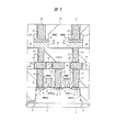
次に、図6に示すように、層間絶縁膜14上にCVD法を用いて酸化シリコン膜からなる層間絶縁膜20を堆積した後、層間絶縁膜20上に、例えば五酸化タンタル(Ta2O5)膜からなる接着層24を形成する。接着層24を形成するには、まず、層間絶縁膜20上にスパッタリング法を用いてTa膜を堆積した後、Ta膜をラジカル酸化することによってTa2O5膜とする。あるいは、酸化雰囲気中でTaターゲットをスパッタすることによって、層間絶縁膜20上にTa2O5膜を直接堆積してもよい。接着層24は、Ta2O5膜に代えて、TiO膜、NbO膜、ZrO膜、HfO膜、CrO膜、MoO膜、WO膜、AlO膜などの誘電体膜で構成することもできる。また、これらの誘電体膜を2層以上積層して接着層24を形成することもできる。
Next, as shown in FIG. 6, an
続いてフォトレジスト膜をマスクにして接着層24および層間絶縁膜20をドライエッチングすることにより、第1層配線18を露出する接続孔21、22を形成する。次に、公知の方法を用いて接続孔21、22の内部にWなどの主導体膜とTi/TiNなどの導電性バリア膜とからなるプラグ23を形成する。接続孔21の内部のプラグ23は、抵抗素子RM1の下部電極を構成し、接続孔22の内部のプラグ23は、抵抗素子RM2の下部電極を構成する。
Subsequently, the contact holes 21 and 22 exposing the
次に、図7に示すように、接着層24上に抵抗素子RM1、RM2を形成する。抵抗素子RM1、RM2を形成するには、まず、接着層24上にスパッタリング法でGeSbTe膜またはInGeSbTe膜などの多元系カルコゲナイド膜を堆積し、続いてこのカルコゲナイド膜上にスパッタリング法でW膜を堆積した後、W膜上にCVD法で酸化シリコン膜からなるキャップ絶縁膜27を堆積する。次に、フォトレジスト膜をマスクにしたドライエッチングでキャップ絶縁膜27、W膜およびカルコゲナイド膜をドライエッチングすることによって、W膜からなる上部電極26およびカルコゲナイド膜からなる記憶層25を形成する。なお、このドライエッチングを行う際、記憶層25の下部以外の領域の接着層24をすべて除去してもよい。
Next, as shown in FIG. 7, resistance elements RM <b> 1 and RM <b> 2 are formed on the
次に、図8に示すように、抵抗素子RM1、RM2の上部にCVD法を用いて酸化シリコン膜からなる層間絶縁膜28を堆積した後、CMP法を用いて層間絶縁膜28の表面を平坦化する。次に、フォトレジスト膜をマスクにして層間絶縁膜28およびキャップ絶縁膜27をドライエッチングすることにより、抵抗素子RM1、RM2のそれぞれの上部電極26を露出する接続孔30、31を形成する。次に、公知の方法を用いて接続孔30、31の内部にWなどの主導体膜とTi/TiNなどの導電性バリア膜とからなるプラグ32を形成する。その後、層間絶縁膜28の上部にスパッタリング法などを用いてAlを主導体膜とする金属膜(図示せず)を堆積した後、フォトレジスト膜をマスクにしてこの金属膜をドライエッチングし、第2層配線33を形成することにより、前記図2に示したメモリセルが完成する。
Next, as shown in FIG. 8, an
上記のように構成されたメモリセルMC11、MC21は、抵抗素子RM1、RM2の記憶層25と層間絶縁膜20との間に接着層24が形成されているので、記憶層25と層間絶縁膜20との密着性が向上し、両者の界面剥離を防止することができる。また、接着層24は、絶縁材料(Ta2O5膜など)で構成されているため、接着層24の横方向(半導体基板1の主面に水平な方向)への電流の流れが生じないことから、書き換え時に大電流を必要としない。
In the memory cells MC11 and MC21 configured as described above, since the
抵抗素子RM1、RM2の下部電極を構成している接続孔21、22の内部のプラグ23と記憶層25は、接着層24を介さずに直接接している。このため、プラグ23(下部電極)と記憶層25との間に電流が直接流れるので、接着層24を構成する元素が書き換えによって記憶層25に拡散する現象が防止できる。これにより、記憶層25の電気抵抗率の経年変化が抑えられるので、信頼性の高い相変化メモリを提供することができる。
The
低抵抗状態(セット状態)のメモリセルに電流を流して高抵抗状態(リセット状態)にするリセット書き換えを行う際には、リセット状態の抵抗をセット状態の抵抗に比べて100倍から1000倍程度まで高くすることが望ましい。これは、メモリセルに電流を流して抵抗値を読み出す際の誤読み出しを防ぐためである。リセット書き換えにより上記の抵抗比を得るためには、本実施の形態のように、プラグ23(下部電極)の表面全体を記憶層25で覆うようにする。これは、プラグ23(下部電極)の表面の一部でも記憶層25で覆われていない箇所があると、その箇所が電流パスとなり、リセット状態の抵抗が減少するからである。
When performing a reset rewrite to pass a current through a memory cell in a low resistance state (set state) to set it to a high resistance state (reset state), the resistance in the reset state is about 100 to 1000 times that in the set state. It is desirable to make it higher. This is to prevent erroneous reading when a resistance value is read by passing a current through the memory cell. In order to obtain the above resistance ratio by reset rewriting, the entire surface of the plug 23 (lower electrode) is covered with the
図9は、リセット書き換え時における記憶層25とプラグ23(下部電極)の界面付近の温度分布を示したものであり、図10のX方向に沿った直線上の温度分布の計算結果の一例を示している。また、図9には、接着層24が無いメモリセルに同じ電流を流した場合の温度分布も示してある。
FIG. 9 shows the temperature distribution near the interface between the
いずれの場合も、記憶層25とプラグ23(下部電極)の界面付近では、プラグ23の中心部の直上において温度が最も高く、プラグ23の中心部から周辺部に近づくに従って温度が低下している。接着層24を有する本発明の場合、プラグ23の直径よりも広い範囲で記憶層25の温度がその融点を超えている。これに対して、接着層24が無い場合は、プラグ23の周辺部において記憶層25の温度がその融点以下になっている領域が存在する。これは、本発明の場合、接着層24を有するためにプラグ23の周辺部の熱抵抗が増えたためと考えられる。熱抵抗の増加分としては、接着層24の熱抵抗以外に、記憶層25とプラグ23の界面の熱抵抗、および接着層24と層間絶縁膜20との界面の熱抵抗が考えられる。
In any case, in the vicinity of the interface between the
界面の熱抵抗の大きさの一例として、例えばMo上に酸化シリコン膜を形成した場合には、両者の界面に酸化シリコン膜の厚さに換算して数十nm程度の熱抵抗が存在することが知られている(「金属」Vol. 70, No.10, page 92-97 株式会社 アグネ技術センター、2000年発行)。すなわち、例えば数nm程度膜厚の薄膜を形成して界面を増やすことにより、増えた膜厚以上に熱抵抗を増やすことができることが知られている。 As an example of the magnitude of the thermal resistance of the interface, for example, when a silicon oxide film is formed on Mo, there is a thermal resistance of about several tens of nanometers in terms of the thickness of the silicon oxide film at the interface between the two. ("Metal" Vol. 70, No. 10, page 92-97 Agne Technology Center Co., Ltd., published in 2000). That is, for example, it is known that the thermal resistance can be increased more than the increased film thickness by forming a thin film with a thickness of about several nm and increasing the number of interfaces.
本発明の相変化メモリも、記憶層25とプラグ23の界面に接着層24を付加したことにより、接着層24自身の熱抵抗以外に界面の熱抵抗が追加された結果、接着層24が無い場合に比べてプラグ23の周辺部の温度が上昇したものと考えられる。
In the phase change memory according to the present invention, the
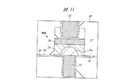
図11は、記憶層とプラグ(下部電極)の間に接着層を設けた相変化メモリの書き換え後における相分布図を示す断面図である。一方、記憶層とプラグ(下部電極)の間に接着層を設けない場合の相分布図を図12に示す。 FIG. 11 is a cross-sectional view showing a phase distribution diagram after rewriting a phase change memory in which an adhesive layer is provided between the memory layer and the plug (lower electrode). On the other hand, FIG. 12 shows a phase distribution diagram when no adhesive layer is provided between the memory layer and the plug (lower electrode).
図11に示すように、接着層24を設けた場合は、プラグ23の上面全体が高抵抗のアモルファス相25aで覆われるため、リセット書き換えの前後で、大きな抵抗値が得られる。しかし、接着層24を設けない場合は、図12に示すように、プラグ23の周辺部が結晶層と接するため、この結晶層が電流パスになり、抵抗値が減少する。すなわち、接着層24が無い場合に大きな抵抗比を得るためには、プラグ23の周辺部にもアモルファス相25aを形成する必要があるので、さらに大きな電流を要することになる。
As shown in FIG. 11, when the
上記のような熱的な観点から考えると、接着層24として有効な材料は、層間絶縁膜20との界面熱抵抗が大きい絶縁材料、または、熱伝導率が層間絶縁膜20よりも低い絶縁材料である。具体的には、TiO、NbO、ZrO、HfO、TaO、CrO、MoO、WO、AlOのいずれかから選ばれた少なくとも一種以上の絶縁材料を用いることが有効である。
Considering from the thermal viewpoint as described above, an effective material for the
次に、本実施の形態のメモリセルの動作原理について説明する。相変化メモリは、DVD記録メディアで用いられている相変化材料を半導体メモリに応用したデバイスである。DVD記録メディアは、レーザパルスにより相変化材料をアモルファス状態または結晶状態に変化させ、アモルファス状態と結晶状態の屈折率の違いにより、情報を記録する。一方、相変化メモリは、メモリセルにパルス電圧を印加し、その電圧とパルス時間を調節することでアモルファス状態か結晶状態かを選択する。その際、電気抵抗がアモルファス状態と結晶状態とで約1000倍以上異なるため、電気抵抗の違いで情報を記録する。 Next, the operation principle of the memory cell of this embodiment will be described. A phase change memory is a device in which a phase change material used in a DVD recording medium is applied to a semiconductor memory. A DVD recording medium changes information of a phase change material to an amorphous state or a crystalline state by a laser pulse, and records information according to a difference in refractive index between the amorphous state and the crystalline state. On the other hand, the phase change memory applies a pulse voltage to a memory cell and adjusts the voltage and pulse time to select an amorphous state or a crystalline state. At that time, since the electric resistance differs by about 1000 times or more between the amorphous state and the crystalline state, information is recorded by the difference in electric resistance.
図13に示すように、メモリセルの結晶状態からアモルファス状態へのスイッチング(リセット)では、比較的大きな電流の短時間パルス(リセットパルス)を流す。一方、アモルファス状態から結晶状態へのスイッチング(セット)では、比較的少ない電流の長時間パルス(セットパルス)を流す。 As shown in FIG. 13, in switching (reset) from the crystalline state to the amorphous state of the memory cell, a short pulse (reset pulse) with a relatively large current is passed. On the other hand, in switching (setting) from the amorphous state to the crystalline state, a long pulse (set pulse) with a relatively small current is passed.
また、読み出し時には、メモリセルに少電流・短時間パルス(リードパルス)を流し、メモリセルの抵抗値から情報を読み出す。リセットパルスでは、大きな電流が流れることによりメモリセルは融解し、パルス幅が短いために冷却が急峻に行なわれることからメモリセルはアモルファス化する。一方、セットパルスでは、メモリセルの温度が結晶化温度を超える程度の電流を流す。これにより、メモリセルがアモルファスから結晶状態へと変化する(図14)。 At the time of reading, a small current / short-time pulse (read pulse) is supplied to the memory cell to read information from the resistance value of the memory cell. In the reset pulse, a large current flows to melt the memory cell, and since the pulse width is short, the memory cell becomes amorphous because cooling is performed sharply. On the other hand, in the set pulse, a current that causes the temperature of the memory cell to exceed the crystallization temperature is passed. As a result, the memory cell changes from an amorphous state to a crystalline state (FIG. 14).
以上、本発明者によってなされた発明を実施の形態に基づき具体的に説明したが、本発明は前記実施の形態に限定されるものではなく、その要旨を逸脱しない範囲で種々変更可能であることはいうまでもない。 As mentioned above, the invention made by the present inventor has been specifically described based on the embodiment. However, the present invention is not limited to the embodiment, and various modifications can be made without departing from the scope of the invention. Needless to say.
前記実施の形態では、プラグ23(下部電極)の上面全体に接着層24を設けないようにしたが、プラグ23(下部電極)の上面の一部に接着層24が残っていてもよい。
In the above embodiment, the
前記実施の形態では、MOSトランジスタと抵抗素子とで構成された相変化メモリについて説明したが、本発明は、バイポーラトランジスタと抵抗素子とで構成された相変化メモリに適用することもできる。 In the above embodiment, the phase change memory composed of the MOS transistor and the resistance element has been described. However, the present invention can also be applied to a phase change memory composed of the bipolar transistor and the resistance element.
本発明は、トランジスタと抵抗素子とで構成された相変化メモリに利用することができる。 The present invention can be used for a phase change memory including a transistor and a resistance element.
1 半導体基板
2 p型ウエル
3 ゲート絶縁膜
4 ゲート電極
5 n−型半導体領域
6 n型半導体領域(ソース、ドレイン)
7 Coシリサイド層
8 サイドウォールスペーサ
9 素子分離溝
10 層間絶縁膜
11、12 接続孔
13 プラグ
14 層間絶縁膜
15、16 配線溝
17、18 第1層配線
20 層間絶縁膜
21、22 接続孔
23 プラグ
24 接着層
25 記憶層
25a アモルファス相
26 上部電極
27 キャップ絶縁膜
28 層間絶縁膜
30、31 接続孔
32 プラグ
33 第2層配線
BL ビット線
MC メモリセル
QD 選択トランジスタ
QM メモリセルトランジスタ
RM 抵抗素子
SA センスアンプ
SL ソース線
Vdd 電源電圧
VGL 電位引抜き線
VPL 電源供給線
WD ワードドライバ
WL ワード線
XDEC ロウデコーダ(Xアドレスデコーダ)
YDEC ビットデコーダ
DESCRIPTION OF
7 Co silicide layer 8
YDEC bit decoder
Claims (11)
前記抵抗素子は、前記トランジスタの上部に形成された層間絶縁膜内の導電性プラグからなる下部電極と、前記層間絶縁膜上に形成された絶縁材料からなる接着層と、前記接着層上に形成された前記相変化材料からなる記憶層と、前記記憶層上に形成された上部電極とを含んで構成され、
前記導電性プラグと前記記憶層は、前記接着層を介することなく直接接していることを特徴とする半導体装置。 A semiconductor device comprising a phase change memory composed of a transistor and a resistance element including a phase change material on a main surface of a semiconductor substrate,
The resistance element is formed on the adhesive layer, a lower electrode made of a conductive plug in an interlayer insulating film formed on the transistor, an adhesive layer made of an insulating material formed on the interlayer insulating film, and A storage layer made of the phase change material formed, and an upper electrode formed on the storage layer,
The semiconductor device, wherein the conductive plug and the memory layer are in direct contact with each other without the adhesive layer interposed therebetween.
(a)前記半導体基板の主面に前記トランジスタを形成する工程、
(b)前記トランジスタの上部に層間絶縁膜を形成した後、前記層間絶縁膜上に絶縁膜を形成する工程、
(c)前記絶縁膜および前記層間絶縁膜をエッチングして接続孔を形成した後、前記接続孔の内部に導電性プラグを形成し、前記トランジスタと前記導電性プラグとを電気的に接続する工程、
(d)前記絶縁膜および前記導電性プラグを覆うように、相変化材料からなる薄膜を形成した後、前記薄膜上に導電膜を形成する工程、
(e)前記導電膜および前記薄膜をパターニングすることにより、前記導電性プラグを下部電極とし、前記相変化材料からなる薄膜を記憶層とし、前記層間絶縁膜と前記記憶層との間に介在する前記絶縁膜を接着層とし、前記導電膜を上部電極とする前記抵抗素子を形成する工程。 A method of manufacturing a semiconductor device including a phase change memory including a transistor and a resistance element including a phase change material on a main surface of a semiconductor substrate,
(A) forming the transistor on a main surface of the semiconductor substrate;
(B) forming an insulating film on the interlayer insulating film after forming an interlayer insulating film on the transistor;
(C) a step of etching the insulating film and the interlayer insulating film to form a connection hole, and then forming a conductive plug in the connection hole to electrically connect the transistor and the conductive plug. ,
(D) forming a conductive film on the thin film after forming a thin film made of a phase change material so as to cover the insulating film and the conductive plug;
(E) By patterning the conductive film and the thin film, the conductive plug serves as a lower electrode, the thin film made of the phase change material serves as a memory layer, and is interposed between the interlayer insulating film and the memory layer. Forming the resistance element using the insulating film as an adhesive layer and the conductive film as an upper electrode;
Priority Applications (1)
| Application Number | Priority Date | Filing Date | Title |
|---|---|---|---|
| JP2007242768A JP2009076596A (en) | 2007-09-19 | 2007-09-19 | Semiconductor device and manufacturing method thereof |
Applications Claiming Priority (1)
| Application Number | Priority Date | Filing Date | Title |
|---|---|---|---|
| JP2007242768A JP2009076596A (en) | 2007-09-19 | 2007-09-19 | Semiconductor device and manufacturing method thereof |
Publications (1)
| Publication Number | Publication Date |
|---|---|
| JP2009076596A true JP2009076596A (en) | 2009-04-09 |
Family
ID=40611317
Family Applications (1)
| Application Number | Title | Priority Date | Filing Date |
|---|---|---|---|
| JP2007242768A Pending JP2009076596A (en) | 2007-09-19 | 2007-09-19 | Semiconductor device and manufacturing method thereof |
Country Status (1)
| Country | Link |
|---|---|
| JP (1) | JP2009076596A (en) |
Cited By (2)
| Publication number | Priority date | Publication date | Assignee | Title |
|---|---|---|---|---|
| US8958229B2 (en) | 2010-06-11 | 2015-02-17 | Samsung Electronics Co., Ltd. | Nonvolatile memory device and method of fabricating same |
| JP2022537312A (en) * | 2019-06-17 | 2022-08-25 | ヘフェイ リライアンス メモリー リミティド | Non-volatile memory cell, non-volatile memory cell array, and method of making same |
-
2007
- 2007-09-19 JP JP2007242768A patent/JP2009076596A/en active Pending
Cited By (4)
| Publication number | Priority date | Publication date | Assignee | Title |
|---|---|---|---|---|
| US8958229B2 (en) | 2010-06-11 | 2015-02-17 | Samsung Electronics Co., Ltd. | Nonvolatile memory device and method of fabricating same |
| JP2022537312A (en) * | 2019-06-17 | 2022-08-25 | ヘフェイ リライアンス メモリー リミティド | Non-volatile memory cell, non-volatile memory cell array, and method of making same |
| JP7383735B2 (en) | 2019-06-17 | 2023-11-20 | ヘフェイ リライアンス メモリー リミティド | Non-volatile memory cells, non-volatile memory cell arrays, and methods of manufacturing the same |
| US11950519B2 (en) | 2019-06-17 | 2024-04-02 | Hefei Reliance Memory Limited | Non-volatile memory cell, non-volatile memory cell array, and method of manufacturing the same |
Similar Documents
| Publication | Publication Date | Title |
|---|---|---|
| JP5145217B2 (en) | Semiconductor device | |
| KR100971832B1 (en) | Semiconductor device | |
| US8427865B2 (en) | Semiconductor storage device | |
| JP4577693B2 (en) | Nonvolatile memory device and manufacturing method thereof | |
| JP5073680B2 (en) | Semiconductor device | |
| JP2007042804A (en) | Semiconductor device and manufacturing method thereof | |
| KR100994866B1 (en) | Semiconductor device, and its manufacturing method | |
| JP4577692B2 (en) | Nonvolatile memory device and manufacturing method thereof | |
| US7977674B2 (en) | Phase change memory device and method of fabricating the same | |
| JP2007073779A (en) | Nonvolatile memory element and its manufacturing method | |
| JP5420436B2 (en) | Nonvolatile memory device and manufacturing method thereof | |
| JP4628935B2 (en) | Nonvolatile semiconductor memory device | |
| JP5634002B2 (en) | Phase change nonvolatile memory and semiconductor device | |
| JP5023072B2 (en) | Semiconductor device manufacturing method and semiconductor device | |
| JP5103470B2 (en) | Semiconductor device and manufacturing method thereof | |
| JP2006351992A (en) | Semiconductor storage device and manufacturing method thereof | |
| JP2009076596A (en) | Semiconductor device and manufacturing method thereof | |
| JPWO2009008080A1 (en) | Semiconductor device |
Legal Events
| Date | Code | Title | Description |
|---|---|---|---|
| A711 | Notification of change in applicant |
Free format text: JAPANESE INTERMEDIATE CODE: A712 Effective date: 20100528 |