JP2009069331A - Transflective liquid crystal display device and electronic apparatus - Google Patents
Transflective liquid crystal display device and electronic apparatus Download PDFInfo
- Publication number
- JP2009069331A JP2009069331A JP2007236281A JP2007236281A JP2009069331A JP 2009069331 A JP2009069331 A JP 2009069331A JP 2007236281 A JP2007236281 A JP 2007236281A JP 2007236281 A JP2007236281 A JP 2007236281A JP 2009069331 A JP2009069331 A JP 2009069331A
- Authority
- JP
- Japan
- Prior art keywords
- liquid crystal
- pixel electrode
- display device
- crystal display
- transflective liquid
- Prior art date
- Legal status (The legal status is an assumption and is not a legal conclusion. Google has not performed a legal analysis and makes no representation as to the accuracy of the status listed.)
- Pending
Links
Images


Abstract
Description
本発明はVA(Vertically Aligned)方式の半透過型液晶表示装置及び電子機器に関する
。更に詳しくは、本発明は、反射部と透過部の境界部分にスリットが形成された画素電極
を備え、反射部の反射効率が良好で明るく、しかも面押し強度が強いVA方式の半透過型
液晶表示装置及び電子機器に関する。
The present invention relates to a VA (Vertically Aligned) type transflective liquid crystal display device and electronic equipment. More specifically, the present invention includes a VA-type transflective liquid crystal having a pixel electrode in which a slit is formed at the boundary between the reflective portion and the transmissive portion, the reflective portion has a good reflection efficiency, is bright, and has a strong surface pressing strength. The present invention relates to a display device and an electronic device.
近年の携帯電話等に代表される携帯型の機器に使用される液晶表示装置としては、透過
型及び反射型の性質を併せ持つ半透過型液晶表示装置が多く使用されるようになっている
。この半透過型液晶表示装置は、個々の画素内に透明電極を備えた透過部と反射層を備え
た反射部を有している。そして、暗い場所においてはバックライトを点灯して個々の画素
の透過部を利用して画像を表示し、明るい場所においてはバックライトを点灯することな
く個々の画素の反射部において外光を利用して画像を表示している。そのため、半透過型
液晶表示装置を使用した表示装置は、常時バックライトを点灯する必要がないので、消費
電力を大幅に低減させることができるという利点を有している。
As a liquid crystal display device used in a portable device typified by a recent cellular phone or the like, a transflective liquid crystal display device having both transmissive and reflective properties is often used. This transflective liquid crystal display device has a transmissive portion having a transparent electrode and a reflective portion having a reflective layer in each pixel. In a dark place, the backlight is turned on and an image is displayed using the transmissive part of each pixel. In a bright place, the external light is used in the reflective part of each pixel without turning on the backlight. The image is displayed. Therefore, a display device using a transflective liquid crystal display device has an advantage that power consumption can be greatly reduced because it is not necessary to always turn on the backlight.
一方、液晶表示装置においては、それぞれの画素電極及び対向電極間の間隔、すなわち
液晶層の厚さ(セルギャップ)を一定とするため、スペーサが必要である。このスペーサ
として、フォトレジストからなる柱状スペーサを使用すると、一方の基板側に一体化して
形成でき、しかも高さを一定にできるとともに表示領域を避けて配置することができるた
めに、表示画質が良好となるという利点を有している。
On the other hand, in the liquid crystal display device, a spacer is necessary in order to keep the distance between each pixel electrode and the counter electrode, that is, the thickness (cell gap) of the liquid crystal layer constant. If a columnar spacer made of photoresist is used as this spacer, it can be formed integrally on one substrate side, and the height can be made constant and the display area can be avoided, so that the display image quality is good. It has the advantage of becoming.
そして、半透過型液晶表示装置においても、セルギャップを一定に保つため柱状スペー
サを設けるものが知られている。例えば、下記特許文献1には、柱状スペーサは部分的に
見えても光学的な影響が少ないため、反射部内に柱状スペーサを形成した例が示されてい
る。また、下記特許文献2には、走査線と信号線の交差部に柱状スペーサを形成した例が
、下記特許文献3には反射部間の信号線上に柱状スペーサを形成した例が、更に下記特許
文献4には反射部のコンタクトホール部に柱状スペーサを形成した例が、それぞれ示され
ている。また、このような柱状スペーサは、一般に各サブ画素毎に1個(下記特許文献2
参照)、2サブ画素毎に1個(下記特許文献5参照)ないし1ピクセル(3サブ画素)毎
に1個(下記特許文献1参照)設けられている。
1) (see Patent Document 5 below) for every 2 sub-pixels, or 1 (see Patent Document 1 below) for every 1 pixel (3 sub-pixels).
このような柱状スペーサが形成された半透過型液晶表示装置においては、例えばアレイ
基板側の表面に柱状スペーサを受ける土台となるスペーサ受け部が形成される。このスペ
ーサ受け部は、液晶表示装置の製造の際の重ねずれ量を考慮して、柱状スペーサの先端部
の大きさよりも少し大きめに形成され、かつ、均一なセルギャップを得るために表面が平
らにされている。しかしながら、上記特許文献1に開示された半透過型液晶表示装置のよ
うに、スペーサ受け部を反射部に設けると、このスペーサ受け部の面積分だけ反射部の面
積が狭くなってしまい、反射率が低くなるという問題点を有している。なお、この明細書
でいう反射部の面積とは、反射板が存在し、かつ、この反射板の表面に凹凸が形成されて
いる部分の面積をいう。すなわち、反射板の表面に凹凸が形成されていないと、反射光は
拡散反射光とならずに鏡面反射光となるため、視覚的には反射率の低下として捉えられる
。そのため、本発明ではこのような反射板の表面に凹凸が形成されていない部分は反射部
の面積としては除外されている。
In the transflective liquid crystal display device in which such columnar spacers are formed, for example, a spacer receiving portion serving as a base for receiving the columnar spacers is formed on the surface on the array substrate side. This spacer receiving portion is formed slightly larger than the size of the tip of the columnar spacer in consideration of the amount of overlap during manufacture of the liquid crystal display device, and the surface is flat to obtain a uniform cell gap. Has been. However, when the spacer receiving portion is provided in the reflecting portion as in the transflective liquid crystal display device disclosed in Patent Document 1, the area of the reflecting portion is reduced by the area of the spacer receiving portion, and the reflectance is reduced. Has a problem of lowering. In addition, the area of the reflection part as used in this specification means the area of the part in which the reflecting plate exists and the unevenness | corrugation is formed in the surface of this reflecting plate. That is, if the surface of the reflector is not uneven, the reflected light is not diffusely reflected light but becomes specularly reflected light, which is visually perceived as a decrease in reflectance. Therefore, in this invention, the part in which the unevenness | corrugation is not formed in the surface of such a reflecting plate is excluded as an area of a reflection part.
一方、柱状スペーサは、多くは円柱状に形成され、その直径は強度及び剥離の問題を勘
案して10μm以上(上記特許文献1の段落[0005]参照)とされている。しかも、
柱状スペーサを受けるスペーサ受け部の面積は、液晶表示装置の製造の際の重ねずれ等を
考慮して、柱状スペーサの断面の面積よりも大きくされている。更に、近年の中型ないし
小型の液晶表示装置においては、高精細化の進展に伴ない、個々の画素の表示に有効な領
域の面積が小さくなると共に、走査線及び信号線の幅が約5μm以下と細くなっている。
On the other hand, many columnar spacers are formed in a columnar shape, and the diameter thereof is 10 μm or more (see paragraph [0005] of Patent Document 1) in consideration of problems of strength and peeling. Moreover,
The area of the spacer receiving portion that receives the columnar spacer is larger than the area of the cross-section of the columnar spacer in consideration of an overlay error at the time of manufacturing the liquid crystal display device. Further, in recent medium-sized or small-sized liquid crystal display devices, with the progress of high definition, the area of an area effective for displaying individual pixels is reduced, and the width of scanning lines and signal lines is about 5 μm or less. It is thin.
そのため、上記特許文献1に開示されている半透過型液晶表示装置のように、柱状スペ
ーサを反射部内に形成した場合には、反射部の反射効率が低下するため、高精細化された
中型ないし小型の半透過型液晶表示装置の構成としては採用し難い。また、上記特許文献
2に開示された半透過型液晶表示装置のように、柱状スペーサを受けるスペーサ受け部の
大部分を走査線と信号線の交差部に設けた場合においても、スペーサ受け部の幅は走査線
ないし信号線よりも広くなっているため、反射部の面積が小さくなって反射効率が低下す
るという問題点を有している。加えて、上記特許文献2に開示された半透過型液晶表示装
置によれば、柱状スペーサを設けないサブ画素も含めて全てのサブ画素に平らなスペーサ
受け部が設けられており、この平らな部分は、たとえ反射板が存在しているとしても、反
射率が低くなってしまう。特に、緑色のサブ画素部分は、人の視感度が最も高いため、反
射効率の低下に起因する表示品位の低下は著しい。
Therefore, as in the transflective liquid crystal display device disclosed in Patent Document 1, when the columnar spacer is formed in the reflection portion, the reflection efficiency of the reflection portion is reduced, so that the high-definition medium-size or It is difficult to adopt as a configuration of a small transflective liquid crystal display device. Further, as in the transflective liquid crystal display device disclosed in the above-mentioned Patent Document 2, even when the most part of the spacer receiving portion that receives the columnar spacer is provided at the intersection of the scanning line and the signal line, Since the width is wider than the scanning line or the signal line, there is a problem that the area of the reflection portion is reduced and the reflection efficiency is lowered. In addition, according to the transflective liquid crystal display device disclosed in Patent Document 2, all the sub-pixels including the sub-pixels not provided with columnar spacers are provided with flat spacer receiving portions. Even if the reflector exists, the reflectance of the portion is low. In particular, since the green sub-pixel portion has the highest human visibility, the deterioration in display quality due to the decrease in reflection efficiency is significant.
更に、上記特許文献3に開示された半透過型液晶表示装置のように、柱状スペーサを受
けるスペーサ受け部を反射部間の信号線と対向する位置に配置されたカラーフィルタ基板
の遮光膜上に形成した場合には、反射受け部の幅は信号線よりも広いため、信号線上に収
まらないスペーサ受け部が信号線の両側の反射部にはみ出す。そのため、上記特許文献3
に開示された半透過型液晶表示装置では、上記特許文献2に開示された発明と同様の問題
点が生じる。また、上記特許文献4に開示されている半透過型液晶表示装置は、反射部に
形成されているコンタクトホールをスペーサ受け部として兼用するものであるため、コン
タクトホールの開口の大きさを柱状スペーサの断面の大きさよりも大きくする必要がある
。そのため、このコンタクトホールの開口の大きさは従来例のものよりも大きくせざるを
得ないが、コンタクトホール部分は反射部の画像表示には関与しないので、反射部の面積
が減少して反射効率が低下する。また、組合せズレなどが生じると、コンタクトホールに
フォトスペーサが勘合できないため、セルギャップが不均一となりセルギャップ不良の発
生が懸念される。
Further, like the transflective liquid crystal display device disclosed in Patent Document 3 above, the spacer receiving portion for receiving the columnar spacer is placed on the light shielding film of the color filter substrate disposed at a position facing the signal line between the reflecting portions. In this case, since the width of the reflection receiving portion is wider than that of the signal line, the spacer receiving portion that does not fit on the signal line protrudes from the reflection portions on both sides of the signal line. Therefore, the above Patent Document 3
In the transflective liquid crystal display device disclosed in 1), problems similar to those of the invention disclosed in Patent Document 2 occur. Further, since the transflective liquid crystal display device disclosed in Patent Document 4 also uses the contact hole formed in the reflection portion as a spacer receiving portion, the size of the contact hole opening is set to a columnar spacer. It is necessary to make it larger than the size of the cross section. For this reason, the size of the contact hole opening must be larger than that of the conventional example, but the contact hole part is not involved in the image display of the reflection part, so the area of the reflection part is reduced and the reflection efficiency is reduced. Decreases. Further, when a misalignment or the like occurs, the photo spacer cannot be fitted into the contact hole, so that the cell gap becomes non-uniform and there is a concern that a cell gap defect may occur.
加えて、昨今の液晶表示装置のエンドユーザーから面押し強度を上げる要求が高まって
いるが、液晶表示装置の面押し強度を上げるためには柱状スペーサの数を増加させること
が必要となる。そうすると、従来例のような柱状スペーサ配置の半透過型液晶表示装置で
は、柱状スペーサの数を増加させると益々反射部の面積が減少して反射効率が低下してし
まう。
In addition, there is an increasing demand for increasing the surface pressing strength by end users of recent liquid crystal display devices, but in order to increase the surface pressing strength of the liquid crystal display device, it is necessary to increase the number of columnar spacers. Then, in the transflective liquid crystal display device having the columnar spacer arrangement as in the conventional example, when the number of the columnar spacers is increased, the area of the reflection portion is decreased and the reflection efficiency is decreased.
本発明は、上述のような従来技術の問題点を解決すべくなされたものであって、特に反
射部と透過部との間画素電極にスリットを形成したVA方式の半透過型液晶表示装置に適
用し得る、反射部の反射効率が良好で明るく、面押し強度が強い半透過型液晶表示装置及
び電子機器を提供することを目的とする。
The present invention has been made to solve the above-described problems of the prior art, and more particularly, to a VA type transflective liquid crystal display device in which a slit is formed in a pixel electrode between a reflective portion and a transmissive portion. An object of the present invention is to provide a transflective liquid crystal display device and an electronic device that can be applied and have a good reflection efficiency of a reflection portion, are bright, and have a strong surface pressing strength.
上記目的を達成するため、本発明の半透過型液晶表示装置は、マトリクス状に配置され
た走査線及び信号線で囲まれたそれぞれの画素領域毎に反射部と透過部とが形成され、前
記反射部の画素電極と前記透過部の画素電極とが連結部の画素電極によって接続されてお
り、前記反射部の画素電極の下部には表面に凹凸が形成された反射板が設けられているア
レイ基板と、平面視で前記透過部の隣接する画素電極間を被覆する遮光膜が形成されたカ
ラーフィルタ基板と、を備えた半透過型液晶表示装置であって、前記反射部の画素電極と
透過部の画素電極との間に位置する前記信号線の対向位置にある前記カラーフィルタ基板
の遮光膜上に柱状スペーサが形成されていることを特徴とする。
In order to achieve the above object, a transflective liquid crystal display device according to the present invention includes a reflective portion and a transmissive portion for each pixel region surrounded by scanning lines and signal lines arranged in a matrix. An array in which a pixel electrode of a reflective portion and a pixel electrode of the transmissive portion are connected by a pixel electrode of a connecting portion, and a reflector having an uneven surface is provided below the pixel electrode of the reflective portion A transflective liquid crystal display device comprising: a substrate; and a color filter substrate on which a light-shielding film that covers between adjacent pixel electrodes of the transmissive portion in plan view is formed, the pixel electrode of the reflective portion being transmissive to the pixel electrode A columnar spacer is formed on the light-shielding film of the color filter substrate at a position facing the signal line located between the pixel electrode and the pixel electrode.
本発明の半透過型液晶表示装置によれば、反射部の画素電極と透過部の画素電極とが連
結部の画素電極によって接続されているため、反射部の画素電極と透過部の画素電極との
間は、透過部としても反射部としても機能しない。したがって、このような透過部として
も反射部としても機能しない部分に位置する信号線の対向位置にあるカラーフィルタ基板
の遮光膜上に柱状スペーサを形成すると、たとえこの柱状スペーサが信号線からはみ出し
ても、少なくとも反射部の画素電極上を覆うことをなくすことができる。そのため、反射
部の反射効率が低下することがなく、反射部の表示が明るい半透過型液晶表示装置が得ら
れる。また、信号線と補助容量線の交差部で発生する寄生容量に起因する不要な電界によ
って生じる光漏れを同時に抑制することが可能となる。
According to the transflective liquid crystal display device of the present invention, since the pixel electrode of the reflection part and the pixel electrode of the transmission part are connected by the pixel electrode of the connection part, the pixel electrode of the reflection part and the pixel electrode of the transmission part are During this time, it does not function as a transmission part or a reflection part. Therefore, if a columnar spacer is formed on the light-shielding film of the color filter substrate at a position opposite to the signal line located in a portion that does not function as a transmission part or a reflection part, even if this columnar spacer protrudes from the signal line. However, it is possible to eliminate covering at least the pixel electrode of the reflective portion. For this reason, a transflective liquid crystal display device in which the reflection efficiency of the reflection portion does not decrease and the display of the reflection portion is bright is obtained. Further, it is possible to simultaneously suppress light leakage caused by an unnecessary electric field due to parasitic capacitance generated at the intersection of the signal line and the auxiliary capacitance line.
加えて、上述のような透過部としても反射部としても機能しない部分はそれぞれの画素
領域毎に存在しているから、柱状スペーサをそれぞれの画素領域毎に形成しても、反射部
の反射効率の低下は少なく、しかも面押し強度が強い半透過型液晶表示装置が得られる。
In addition, since there is a part that does not function as a transmission part or a reflection part as described above for each pixel area, even if a columnar spacer is formed for each pixel area, the reflection efficiency of the reflection part Thus, a transflective liquid crystal display device having a small surface degradation and high surface pressing strength can be obtained.
また、本発明の半透過型液晶表示装置においては、前記柱状スペーサの横断面は円形状
、楕円形状、多角形状又は角が丸められた多角形状とされていることが好ましい。
In the transflective liquid crystal display device of the present invention, it is preferable that a cross section of the columnar spacer is circular, elliptical, polygonal, or polygonal with rounded corners.
係る態様の半透過型液晶表示装置によれば、反射部の反射効率に影響を与えることなく
スペーサ受け部の面積を大きくすることができる。柱状スペーサの断面の形状が多角形状
又は角が丸められた多角形状であっても円形に近い形にすることができるだけでなく、円
形状ないし楕円形状とすることもできる。特に柱状スペーサの断面の形状が円形状ないし
楕円形状であると、断面が多角形状又は角が丸められた多角形状のものよりも四方から加
わる力に対する曲げ応力が強くなる。従って、係る態様の半透過型液晶表示装置によれば
、外部から半透過型液晶表示装置の表面対して部分的に応力が印加されても、セルギャッ
プの変動が少なくなるため、表示画質の低下が少なくなる。
According to the transflective liquid crystal display device of this aspect, the area of the spacer receiving portion can be increased without affecting the reflection efficiency of the reflecting portion. Even if the cross-sectional shape of the columnar spacer is a polygonal shape or a polygonal shape with rounded corners, it can be not only a circular shape but also a circular or elliptical shape. In particular, when the cross-sectional shape of the columnar spacer is a circular shape or an elliptical shape, bending stress with respect to a force applied from four directions becomes stronger than that of a polygonal shape with a polygonal cross section or rounded corners. Therefore, according to the transflective liquid crystal display device of this aspect, even if a stress is partially applied to the surface of the transflective liquid crystal display device from the outside, the variation in cell gap is reduced, so that the display image quality is deteriorated. Less.
また、本発明の半透過型液晶表示装置においては、前記反射部の画素電極及び透過部の
画素電極は、互いに対向する側の角部が共に切り落とされていることが好ましい。
In the transflective liquid crystal display device according to the present invention, it is preferable that the pixel electrode of the reflective portion and the pixel electrode of the transmissive portion are both cut off at opposite corners.
係る態様の半透過型液晶表示装置によれば、前記反射部の画素電極及び透過部の画素電
極の互いに対向する部分の角部を切り落とすことにより、画素電極内の電界が均一にかか
り易くなり液晶分子の配向の乱れが少なくなるので、表示画質が良好な半透過型液晶表示
装置が得られる。更に、透過部の切り落とされた画素電極のエッジ部は、液晶分子の配向
規制手段として機能するため、広視野角の半透過型液晶表示装置が得られる。
According to the transflective liquid crystal display device of this aspect, the electric field in the pixel electrode is easily applied uniformly by cutting off the corner portions of the pixel electrode of the reflection portion and the pixel electrode of the transmission portion facing each other. Since the disorder of molecular orientation is reduced, a transflective liquid crystal display device with good display image quality can be obtained. Further, since the edge portion of the pixel electrode from which the transmissive portion is cut off functions as a liquid crystal molecule alignment regulating means, a transflective liquid crystal display device having a wide viewing angle can be obtained.
また、本発明の半透過型液晶表示装置においては、前記柱状スペーサは少なくとも1ピ
クセルに1本形成されていることが好ましい。
In the transflective liquid crystal display device of the present invention, it is preferable that at least one columnar spacer is formed per pixel.
柱状スペーサの数に比例して面押しに対する耐力は強くなるが、柱状スペーサの存在に
よる柱状スペーサの周囲の液晶分子の配向に対する悪影響も大きくなる。しかしながら、
本発明の半透過型液晶表示装置によれば柱状スペーサは透過部でも反射部でもない位置に
形成されているため、柱状スペーサの周囲の液晶分子の配向に対する悪影響は従来例のも
のに比すると非常に小さい。従って、本発明の半透過型液晶表示装置のように、1ピクセ
ルに少なくとも1本の柱状スペーサを形成すれば、面押し強度と表示画質の調和が取れた
半透過型液晶表示装置が得られる。
Although the resistance to surface pressing increases in proportion to the number of columnar spacers, the presence of the columnar spacers also increases the adverse effect on the alignment of liquid crystal molecules around the columnar spacers. However,
According to the transflective liquid crystal display device of the present invention, since the columnar spacer is formed at a position that is neither a transmissive part nor a reflective part, the adverse effect on the alignment of the liquid crystal molecules around the columnar spacer is much higher than that of the conventional example. Small. Accordingly, as in the transflective liquid crystal display device of the present invention, when at least one columnar spacer is formed in one pixel, a transflective liquid crystal display device in which the surface pressing strength and the display image quality are balanced can be obtained.
また、本発明の半透過型液晶表示装置においては、前記カラーフィルタ基板には、平面
視で前記透過部の隣接する画素電極間を被覆する遮光膜が形成されており、前記柱状スペ
ーサは平面視で前記透過部の隣接する画素電極間を被覆する遮光膜の端部に形成されてい
ることが好ましい。
In the transflective liquid crystal display device of the present invention, the color filter substrate is formed with a light-shielding film covering between adjacent pixel electrodes of the transmissive portion in plan view, and the columnar spacer is seen in plan view. It is preferable that the light-shielding film is formed at the end of the light-shielding film that covers the adjacent pixel electrodes of the transmissive part.
本来、透過部の隣接する画素電極間の下部には信号線が存在しているため、透過部の隣
接する画素電極間から光漏れすることはない。しかし、マスクずれ等によって透過部の画
素電極が信号線の表面に部分的に重複しない場合がある。そのため、平面視で透過部の隣
接する画素電極間を遮光膜で被覆することにより、このような光漏れを抑制することがで
きるようになる。また、この遮光膜の端部に柱状スペーサが配置されているため、柱状ス
ペーサが外部から視認し難くなり、コントラストが良好で、表示品質の良好な半透過型液
晶表示装置が得られる。
Originally, since a signal line exists below the pixel electrodes adjacent to each other in the transmissive part, light does not leak from between the pixel electrodes adjacent to each other in the transmissive part. However, the pixel electrode in the transmissive part may not partially overlap the surface of the signal line due to mask displacement or the like. For this reason, such a light leakage can be suppressed by covering the pixel electrodes adjacent to each other in the plan view with a light shielding film. In addition, since the columnar spacer is disposed at the end of the light-shielding film, the columnar spacer becomes difficult to visually recognize from the outside, and a transflective liquid crystal display device with good contrast and good display quality can be obtained.
また、本発明の半透過型液晶表示装置においては、前記カラーフィルタ基板には前記透
過部の画素電極と反射部の画素電極との間を被覆する遮光膜が形成されており、前記透過
部の隣接する画素電極間を被覆する遮光膜は前記透過部の画素電極と反射部の画素電極と
の間を被覆する遮光膜と一体化されており、前記透過部の画素電極と反射部の画素電極と
の間を被覆する遮光膜は前記透過部の画素電極と反射部の画素電極との間を被覆する遮光
膜の端部にアイランド状に形成されていることが好ましい。
In the transflective liquid crystal display device of the present invention, a light-shielding film is formed on the color filter substrate to cover a space between the pixel electrode of the transmissive part and the pixel electrode of the reflective part. A light-shielding film covering between adjacent pixel electrodes is integrated with a light-shielding film covering between the pixel electrode of the transmissive part and the pixel electrode of the reflective part, and the pixel electrode of the transmissive part and the pixel electrode of the reflective part It is preferable that the light shielding film covering the gap between the transparent electrode and the pixel electrode of the reflective part is formed in an island shape at the end of the light shielding film.
本来、透過部の画素電極と反射部の画素電極との間には垂直配向膜が形成されているこ
と及び反射部の画素電極の下部には補助容量線が配置されているため、この部分から光漏
れすることはない。しかしながら、信号線及び補助容量線の交差部で寄生容量を持ちやす
く、不要な電界により光リークが発生しやすくなる。また、マスクずれ等によって補助容
量線側からの漏れ光が信号線上から漏れる可能性があるが、平面視で透過部の隣接する画
素電極間を被覆する遮光膜を透過部の画素電極と反射部の画素電極との間を被覆する遮光
膜と一体に形成し、反射部にも透過部にも寄与しない信号線と補助容量線の交差部にアイ
ランド状の遮光膜を形成することにより、このような光漏れを抑制することができるよう
になる。また、柱状スペーサの幅が信号線の幅よりも大きくても、柱状スペーサに対応す
る位置及び透過部の隣接する画素電極間を同時に遮光することができるようになり、より
コントラストが良好で、表示品質の良好な半透過型液晶表示装置が得られる。
Originally, a vertical alignment film is formed between the pixel electrode of the transmissive part and the pixel electrode of the reflective part, and an auxiliary capacitance line is disposed below the pixel electrode of the reflective part. There is no light leakage. However, it is easy to have a parasitic capacitance at the intersection of the signal line and the auxiliary capacitance line, and light leakage is likely to occur due to an unnecessary electric field. Further, there is a possibility that leakage light from the auxiliary capacitance line side leaks from the signal line due to mask displacement or the like, but the light shielding film that covers the pixel electrodes adjacent to each other in the plan view is arranged as a pixel electrode and a reflection portion in the transmission portion By forming an island-shaped light shielding film at the intersection of the signal line and the auxiliary capacitance line that does not contribute to the reflection part and the transmission part, the light shielding film is formed integrally with the pixel electrode. Light leakage can be suppressed. In addition, even if the width of the columnar spacer is larger than the width of the signal line, the position corresponding to the columnar spacer and the adjacent pixel electrodes of the transmission part can be shielded at the same time. A transflective liquid crystal display device with good quality can be obtained.
また、本発明の半透過型液晶表示装置においては、前記カラーフィルタ基板の少なくと
も前記透過部に対応する位置には液晶分子の配向規制手段が形成されていることが好まし
い。
In the transflective liquid crystal display device of the present invention, it is preferable that alignment regulating means for liquid crystal molecules is formed at a position corresponding to at least the transmission part of the color filter substrate.
このような構成とすると、カラーフィルタ基板側においても各画素領域内で液晶分子の
配向方向を複数の異なる方向に分割されるように配向規制することができる。従って、更
に広視野角を達成できるMVA(Multi-domain Vertically Aligned)方式の半透過型液晶
表示装置が得られる。なお、この配向規制手段は透過部だけでなく反射部に形成してもよ
い。なお、この配向規制手段は、共通電極の表面に形成した突起又は共通電極に形成した
スリットからなるものとすることができる。
With such a configuration, it is possible to regulate the alignment so that the alignment direction of the liquid crystal molecules is divided into a plurality of different directions in each pixel region also on the color filter substrate side. Therefore, a transflective liquid crystal display device of MVA (Multi-domain Vertically Aligned) system that can achieve a wider viewing angle can be obtained. In addition, you may form this orientation control means not only in a transmission part but in a reflection part. In addition, this orientation control means can consist of the protrusion formed in the surface of the common electrode, or the slit formed in the common electrode.
更に、本発明の電子機器は前記いずれかに記載の半透過型液晶表示装置を備えたことを
特徴とする。
Furthermore, an electronic apparatus according to the present invention includes any one of the above-described transflective liquid crystal display devices.
本発明の電子機器によれば、反射部n反射効率が良好で明るく、しかも面押し強度が強
いVA方式の半透過型液晶表示装置を備えた電子機器が得られる。
According to the electronic apparatus of the present invention, it is possible to obtain an electronic apparatus including a VA-type transflective liquid crystal display device that has a good reflection portion n reflection efficiency, is bright, and has strong surface pressing strength.
以下、本発明を実施するための最良の形態を実施例及び図面を用いてより具体的に説明
する。なお、以下に示す実施例は、本発明の技術思想を具体化するための半透過型液晶表
示装置を示すものであるが、本発明をここに記載したものに限定することを意図するもの
ではなく、本発明は特許請求の範囲に示した技術思想を逸脱することなく種々の変更を行
ったものにも均しく適用し得るものである。
Hereinafter, the best mode for carrying out the present invention will be described more specifically with reference to examples and drawings. In addition, although the Example shown below shows the transflective liquid crystal display device for actualizing the technical idea of this invention, it does not intend limiting this invention to what was described here. The present invention can be equally applied to various modifications without departing from the technical idea shown in the claims.
なお、図1は実施例1のVA方式の半透過型液晶表示装置の3サブ画素部分をカラーフ
ィルタ層を透視して表した概略平面図である。図2はカラーフィルタ基板の遮光膜を含め
て表した図1に対応する概略平面図である。図3は図1のIII−III線に沿った断面図であ
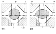
る。図4は図1の破線で囲んだ領域IV部分の拡大図である。図5A及び図5Bは実施例1
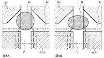
の第1及び第2の変形例の図4に対応する拡大図である。図6A及び図6Bは実施例1の
第3及び第4の変形例の図4に対応する拡大図である。図7は第3及び第4の変形例の場
合のカラーフィルタ基板の遮光膜を含めて表した図1に対応する概略平面図である。図8
は実施例1の第5及び第6の変形例の図4に対応する拡大図である。図9は実施例2のM
VA方式の半透過型液晶表示装置の3サブ画素部分をカラーフィルタ層を透視して表した
概略平面図である。図10は図9のX−X線に沿った断面図である。図11Aは本発明の
半透過型液晶表示装置を備えたパーソナルコンピュータを示す図であり、図11Bは本発
明の半透過型液晶表示装置を備えた携帯電話機を示す図である。
FIG. 1 is a schematic plan view showing the three sub-pixel portions of the VA-type transflective liquid crystal display device of Example 1 through a color filter layer. FIG. 2 is a schematic plan view corresponding to FIG. 1 and including the light shielding film of the color filter substrate. FIG. 3 is a sectional view taken along line III-III in FIG. 4 is an enlarged view of a region IV portion surrounded by a broken line in FIG. 5A and 5B show the first embodiment.
It is an enlarged view corresponding to FIG. 4 of the 1st and 2nd modification of this. 6A and 6B are enlarged views corresponding to FIG. 4 of the third and fourth modifications of the first embodiment. FIG. 7 is a schematic plan view corresponding to FIG. 1 including the light shielding film of the color filter substrate in the case of the third and fourth modifications. FIG.
These are the enlarged views corresponding to FIG. 4 of the 5th and 6th modification of Example 1. FIG. FIG. 9 shows M in Example 2.
FIG. 3 is a schematic plan view illustrating three sub-pixel portions of a VA type transflective liquid crystal display device as seen through a color filter layer. FIG. 10 is a cross-sectional view taken along line XX in FIG. FIG. 11A is a diagram showing a personal computer equipped with the transflective liquid crystal display device of the present invention, and FIG. 11B is a diagram showing a mobile phone equipped with the transflective liquid crystal display device of the present invention.
まず、図1〜図4に基づいて実施例1に係るVA方式の半透過型液晶表示装置10Aに
ついて説明する。このVA方式の半透過型液晶表示装置10Aは、互いに対向配置された
アレイ基板AR及びカラーフィルタ基板CFを備えている。アレイ基板ARは、ガラス基
板等からなる透明基板11の表面にマトリクス状に形成された複数本の走査線12及び信
号線13と、これらの走査線12間に走査線12と平行に設けられた補助容量線14が設
けられている。そして、走査線12と信号線13とで囲まれたそれぞれの領域には、ソー
ス電極S、ゲート電極G、ドレイン電極D、及び半導体層15とからなる薄膜トランジス
タ(TFT:Thin Film Transistor)と、画素電極16とが形成されている。ここで、そ
れぞれの走査線12と信号線13とで囲まれた領域が1サブ画素に相当する。
First, a VA transflective liquid
走査線12、ゲート電極G、補助容量線14及び露出している透明基板11の表面は第
1の絶縁膜(ゲート絶縁膜ともいわれる)17によって被覆されている。この第1の絶縁
膜17の表面には、例えばアモルファスシリコン(a−Si)層とその表面に形成された
オーミックコンタクト層となるn+a−Si層とからなる半導体層15、ソース電極S及
びドレイン電極Dが形成されているとともに、ソース電極Sに連なる信号線13も形成さ
れている。更に、TFT及び信号線13の表面と、露出している第1の絶縁膜17の表面
全体が第2の絶縁膜(保護絶縁膜ないしパッシベーション膜ともいわれる)18によって
被覆されている。そして、ドレイン電極Dは第1の絶縁膜17の表面を補助容量線14の
上部にまで延在されており、このドレイン電極Dと補助容量線14との間で補助容量が形
成されている。
The scanning lines 12, the gate electrodes G, the
更に、この第2の絶縁膜18の表面には、反射部19においては表面に微細な凹凸部が
形成され、透過部20においては表面が平坦に形成された、フォトレジスト等の有機絶縁
膜からなる層間膜(平坦化膜ともいわれる)21が形成されている。そして、反射部19
においては、層間膜21の表面にはアルミニウム、アルミニウム合金等からなる反射板2
2が形成され、補助容量線14上に位置する第2の絶縁膜18及び層間膜21にはコンタ
クトホール23が形成されている。
Further, the surface of the second insulating
In FIG. 2, the surface of the
2 is formed, and a
この反射部19の反射板22の表面及び透過部20の層間膜21の表面にはITO(In
dium Tin Oxide)やIZO(Indium Zinc Oxide)等の透明導電性材料からなる画素電極
16が形成されている。また、画素電極16は反射部19に形成されたコンタクトホール
23を介してドレイン電極Dと電気的に接続されている。なお、図1〜図4においては反
射部19の凹凸部は省略してある。
ITO (In) is formed on the surface of the reflecting
A
また、この実施例1の半透過型液晶表示装置10Aにおいては、画素電極16の反射部
19と透過部20の境界領域に透明導電性材料が存在していないスリット部24が設けら
れている。従って、画素電極16は、実質的に反射部19の画素電極16aと透過部20
の画素電極16bに分割されており、反射部19の画素電極16aと透過部20の画素電
極16bとは連結部25の画素電極16cを介して電気的に接続されている。この実施例
1のVA方式の半透過型液晶表示装置10Aでは、連結部25の画素電極16cは隣り合
う信号線13の間の略中間に位置している。また連結部25の画素電極16cの幅は走査
線12が延在する方向における反射部19の画素電極16a及び透過部20の画素電極1
6bの幅よりも大幅に狭くなっている。このような構成を採用した理由は、反射部19の
画素電極16a及び透過部20の画素電極16bそれぞれのエッジ部で液晶分子の配向方
向を規制して視野角が広くなるようにするためである。
Further, in the transflective liquid
The
It is much narrower than the width of 6b. The reason for adopting such a configuration is to restrict the alignment direction of the liquid crystal molecules at the edge portions of the
なお、反射部19側においては、補助容量線14は層間膜21の反射板22が存在する
位置の下側に配置されている。また、反射板22及び反射部の画素電極16aは、平面視
で隣接する画素の反射板及び画素電極とは接しないように、走査線12及び信号線13と
は部分的に重複するように設けられ、かつ、反射板22と反射部19の画素電極16aと
は互いに重なるように実質的に同じ形状に設けられている。更に、透過部20側における
画素電極16bは、平面視で隣接する画素の画素電極及び反射板とは接しないように、か
つ、信号線13とは実質的に重複しないように信号線13に沿うように設けられ、また、
走査線12とは若干重なるように形成されている。
On the
The
更に、この実施例1の半透過型液晶表示装置10Aにおいては、透過部20の画素電極
16bは、反射部19の画素電極16aよりも面積が大きくされている。このように、透
過部20の画素電極16bの面積を大きくした理由は、例えば携帯電話機用の半透過型液
晶表示装置は、高精細であってしかも画像表示が多いため、バックライトを常時点灯して
実質的に透過型液晶表示装置として使用される機会が多くなっているためである。そして
、画素電極16の表面をも含み、アレイ基板ARの表面には全ての表示領域を覆うように
して垂直配向膜(図示せず)が積層されている。
Further, in the transflective liquid
なお、この実施例1における透過部20の画素電極16bにおいては、反射部19の画
素電極16aと対向する角部は切り落とされた形状をしている。このような構成とした理
由は、液晶分子の配向規制方向が可能な限り等方的となるようにして視野角が広くなるよ
うにするためである。
Note that, in the
また、カラーフィルタ基板CFのガラス基板等からなる透明基板26の表示領域上には
、図2に示したように、アレイ基板の走査線12及び信号線13に対応する位置にマトリ
クス状に遮光膜30が形成されている。このうち、遮光膜301は平面視で透過部20の
隣接する画素の画素電極16b間を被覆するように形成されている。そして、アレイ基板
ARのスリット部24に対応する位置のアイランド状の遮光膜302上には柱状スペーサ
40が形成されている。
Further, on the display region of the
この柱状スペーサ40は、面押し強度向上の観点から、少なくとも1ピクセルに1個形
成すればよい。しかしながら、この実施例1の半透過型液晶表示装置10Aでは、柱状ス
ペーサ40は反射部19ではなくかつ透過部20でもない位置に対向するカラーフィルタ
基板上のアイランド状遮光膜302上に形成されているため、柱状スペーサ40が液晶分
子の配向に影響を与えることは少ない。そのため、実施例1の半透過型液晶表示装置10
Aでは、必要であれば全てのサブ画素毎に柱状スペーサ40を形成することもできる。
One
In A, if necessary, the
本来、透過部20の隣接する画素の画素電極16b間の下部には信号線13が存在して
いるため、透過部20の隣接する画素の画素電極16b間から光漏れすることはない。し
かし、マスクずれ等によって透過部20の画素電極16bが信号線13の表面に部分的に
重複しない場合があり、また、補助容量線14側からの漏れ光が信号線13上から漏れる
可能性がある。そのため、平面視で透過部20の隣接する画素の画素電極16b間を被覆
する遮光膜301をスリット部24部分を被覆するアイランド状の遮光膜302と一体に
形成することにより、このような光漏れを抑制することができるようになる。
Originally, since the
また、信号線13と補助容量線14との交差部近傍で、寄生容量により不要な電界が発
生して局所的に光リークが発生する。この光リークを抑制するためには、夫々の信号線13
及び補助容量線14の交差部の配線を細らして寄生容量を減らす方法が考えられたが、そ
れにより断線等の副次的な不良が発生した。本来、反射部19及び透過部20の境界部は
反射にも透過にも寄与しないため、デッドスペースとなっていた。そこで走査線13と補
助用稜線14との交差部にアイランド状の遮光膜302を形成して、隣接する透過部20
の画素電極16b間に配置されている遮光膜の端部にアイランド状の遮光膜302を一体
化させて形成することにより、柱状スペーサ40の幅が信号線13幅よりも大きくても、
柱状スペーサ40に対応する位置及び隣接する透過部20の画素電極16b間を同時に遮
光することができるようになる。加えて、このスリット部24部分を被覆する遮光膜30
2上に柱状スペーサ40が配置されているため、柱状スペーサ40が外部から視認し難く
なる。
Further, in the vicinity of the intersection between the
In addition, a method of reducing the parasitic capacitance by thinning the wiring at the intersection of the
By so integrating the island-shaped light-shielding
The position corresponding to the
Since the
なお、本実施例では、アイランド状の遮光膜302と対向する位置のアレイ基板AR側
の最表面には、平坦化された層間膜21上に配向膜が成膜されている為、平坦化を図る為
のフォトスペーサ受け部(図示せず)は必要ない。しかし、本来平坦化を図る為に、アレ
イ基板AR側に層間膜21と同材料でフォトスペーサ受け部を同時形成する。この時、工
程数を増加させる事無くフォトスペーサ受け部を形成出来る。例えば本実施例とは別の構
造を採用し平坦化が図れない場所には、フォトスペーサ受け部を形成しても良い。
In this embodiment, the island-shaped light-shielding
なお、実施例1の液晶表示装置10Aにおいては、反射部19の反射率を向上させるた
め、反射部19の画素電極16a間の信号線13に対応する位置の遮光膜は削除してある
。この理由は、反射部19の信号線13上には平面視で部分的に反射板22が走査線13
に重畳するように形成されているため、この部分からの光漏れの虞は少ないためである。
In the liquid
This is because there is little risk of light leakage from this portion.
そして、カラーフィルタ基板CFの透明基板26上及びマトリクス状に形成された遮光
膜30上には、それぞれの画素に対応して形成される例えば赤色(R)、緑色(G)、青
色(B)のうち何れか一色からなるストライプ状のカラーフィルタ層27が設けられてい
る。更に、反射部19のカラーフィルタ層27の一部分に所定の厚さのトップコート層2
8が設けられている。このトップコート層28は、反射部19全体にわたって設けられて
おり、その厚さは反射部19における液晶層32の厚さ、いわゆるセルギャップが透過部
20のセルギャップの半分となるようにされている。また、トップコート層28の表面及
び露出しているカラーフィルタ層27表面はITOないしIZOからなる共通電極29で
被覆されており、この共通電極29の表面には垂直配向膜(図示せず)が形成されている
。
On the
8 is provided. The
そして、前記アレイ基板AR及びカラーフィルタ基板CFを互いに対向させ、両基板の
周囲にシール材を設けることにより両基板を貼り合せ、両基板間に負の誘電異方性を有す
る液晶分子からなる液晶層32を設けることにより、実施例1のVA方式の半透過型液晶
表示装置10Aが形成される。なお、この半透過型液晶表示装置10Aのアレイ基板AR
の下方には、図示しない周知の光源、導光板、拡散シート等を有するバックライト装置が
配置されている。
Then, the array substrate AR and the color filter substrate CF are opposed to each other, and a sealing material is provided around both substrates to bond both substrates, and a liquid crystal composed of liquid crystal molecules having negative dielectric anisotropy between the substrates. By providing the
A backlight device having a well-known light source, a light guide plate, a diffusion sheet, and the like (not shown) is disposed below.
なお、VA方式の半透過型液晶表示装置10Aにおいては、本来液晶分子に電界が印加
されていない状態で垂直に配向されている限りは液晶層32を光が透過することはない。
従って、画素電極16に設けられたスリット部24の部分にも垂直配向膜が設けられてい
るので、このスリット部24の部分は光が透過することがないため、この実施例1のVA
方式の半透過型液晶表示装置10Aとしては、補助容量線14と信号線13との重なり合
わせ面積を小さくすることにより、寄生容量の発生を抑制して消費電力を防ぐことが可能
となるように、補助容量線14の線幅を走査線13と重なり合わさる箇所だけ細く形成し
ている。また、補助容量が大きくなるようにするために、補助容量線14を反射板22の
下部から更に透過部20側のスリット部24側にまで延長してある。
In the VA-type transflective liquid
Accordingly, since the vertical alignment film is also provided in the
In the transflective liquid
また、この実施例1のVA方式の半透過型液晶表示装置10Aにおいては、透過部20
側の画素電極16bを信号線13とは実質的に重複しないように信号線13に沿うように
設けた例を示した。しかしながら、透過部20の画素電極16bを正確に信号線13に沿
って設けることは技術的に困難であるため、透過部20の画素電極16bと信号線13と
の間に僅かな隙間が生じるようにしてもよく、逆にわずかに透過部20の画素電極16b
と信号線13とが重なるようにしてもよい。透過部20の画素電極16bと信号線13と
の間に僅かな隙間が生じても、この隙間の部分には垂直配向膜が設けられているため、本
来はこの隙間の部分から光漏れすることはない。
In the VA-type transflective liquid
The example in which the
And the
なお、上記実施例1の半透過型液晶表示装置10Aでは、柱状スペーサ40の断面形状
をスリット部24の形状として三角形の角部を切り落とした形状のものとした例を示した
。しかしながら、柱状スペーサ40としては、これに限らず、第1及び第2変形例として
図5A及び図5Bに示したような三角形状のもの、角が丸められた三角形状のものを使用
でき、更には4角以上の多角形上のものや角を丸めた多角形状のもの(図示せず)も使用
し得る。
In the transflective liquid
また、液晶表示装置の面押し強度を強くするには、柱状スペーサ40の断面形状を、第
3変形例及び第4変形例として図6A及び図6Bに示したような円形状ないし楕円形状と
することが好ましい。このような断面形状が円形ないし楕円形状の柱状スペーサ40を採
用した実施例1の変形例の半透過型液晶表示パネル10A'の場合、カラーフィルタ基板
CFの遮光膜30を含めて表した図1に対応する概略平面図は、図7に示したとおりとな
る。
Further, in order to increase the surface pressing strength of the liquid crystal display device, the cross-sectional shape of the
なお、柱状スペーサ40を形成する際に、柱状スペーサ40が反射部19の画素電極1
6aや反射板22の角部と重なって配置したとしても、画素電極16a及び16bの膜圧
はセルギャップに大きな影響を与えることは無い。しかしながら、上記実施例1の半透過
型液晶表示装置10A及びこの変形例の半透過型液晶表示装置10A'では、スリット部
24の幅が狭いため、柱状スペーサ40の断面形状が円形状ないし楕円形状のもので断面
積が大きなものを使用すると、反射部19の画素電極16aと重なってしまうことがある
。この場合は、面押し強度が向上するが、液晶分子の配向不良が顕著に現れやすくなる。
In addition, when forming the
Even if it is arranged so as to overlap the corners of 6a and the reflecting
このような場合、第5変形例及び第6変形例として図8A及び図8Cに示したように、
予め反射部19の画素電極16a及び反射板22の角部を切り落としておくことにより、
柱状スペーサ40として断面積が大きな断面形状が円形状ないし楕円形状のものを使用で
きるようになり、更には正多角形状ないし角が丸められた正多角形状(図示せず)のもの
も使用し得るようになる。このような構成を採用すると、柱状スペーサ40と反射部の画
素電極との重なり部分での配向不良が軽減される上に、画素電極16aの角部を切り落と
して多角形状にすることにより、電界が均一にかかり液晶配向が向上しやすくなる。その
ため、表示画質が良好な半透過型液晶表示装置が得られる。更に、透過部の切り落とされ
た画素電極のエッジ部は、液晶分子の配向規制手段として機能するため、広視野角の半透
過型液晶表示装置が得られる。なお、図5〜図8においては、図1〜図4に示した構成と
同一の構成部分には同じ参照符号を付与してその詳細な説明は省略する。
In such a case, as shown in FIGS. 8A and 8C as the fifth modification and the sixth modification,
By cutting off the
As the
実施例1の半透過型液晶表示装置10Aとしては、カラーフィルタ基板CFに配向規制
手段を形成していない例を示したが、本発明はカラーフィルタ基板CFに配向規制手段を
形成したMVA方式の半透過型液晶表示装置に対しても適用可能である。このカラーフィ
ルタ基板CFに配向規制手段を形成した実施例2のMVA方式の半透過型液晶表示装置1
0Bを図7及び図8を用いて説明するが、実施例1の半透過型液晶表示装置10Aと同一
の構成部分には同一の参照符号を付与してその詳細な説明は省略する。なお、実施例2の
半透過型液晶表示装置10Bにおいても、柱状スペーサの断面形状、スペーサ受け部の形
状、柱状スペーサの形成位置等については実施例1の半透過型液晶表示装置10Aの場合
と同様である。
As the transflective liquid
7B will be described with reference to FIGS. 7 and 8, but the same reference numerals are given to the same components as those of the transflective liquid
この実施例2の半透過型液晶表示装置10Bが実施例1の半透過型液晶表示装置10A
と構成が相違している点は、共通電極29の表面の一部に、
(1)反射部19のコンタクトホール23に対向する位置に底面が円形状の突起311が
設けられている点、及び、
(2)透過部20の画素電極16bに対向する位置に底面が長十字状の突起312が設け
られている点、
である。
The transflective liquid
The configuration is different from the part of the surface of the
(1) that the bottom surface at a position opposite to the
(2) that the bottom long cross-shaped projection 31 2 is provided at a position facing the
It is.
そして、これらの共通電極29、突起311及び312の表面には垂直配向膜(いずれ
も図示せず)が積層されている。このように、実施例2のVA方式の半透過型液晶表示装
置10Bは、透過部20、反射部19の領域にそれぞれ別々に形成された突起311及び
312によって、透過部20、反射部19のそれぞれの領域でカラーフィルタ基板CF側
でも液晶分子の配向が規制されるようになっている。従って、実施例2の半透過型液晶表
示装置10Bによれば、視野角が広く、明るい表示のMVA方式の半透過型液晶表示装置
10Bが得られる。
Then, these
なお、実施例2で、反射部のコンタクトホール23に対向する位置に液晶分子の配向を
規制するための突起311を設けた理由は次のとおりである。コンタクトホール23内の
液晶分子は、電界無印加時でも傾いており、コンタクトホール23の周囲の液晶分子の配
向状態とは差異が生じる。しかも、コンタクトホール23は反射部19に配置されたTF
Tのドレイン電極Dと反射部19の画素電極16aとの間の電気的導通を確実に行うため
にある程度の大きさが必要とされる。そのため、反射部19のコンタクトホール23部分
では液晶分子の配向が乱れているために表示画質が低下する。しかしながら、カラーフィ
ルタ基板CFのコンタクトホール23に対向する位置に液晶分子の配向を規制するための
配向規制手段を設けると、この配向規制手段によって強制的に液晶分子の配向が規制され
るため、反射部19の表示画質の低下を抑制することができる。
In Example 2, the reason for providing the protrusion 31 1 for controlling the alignment of liquid crystal molecules at a position opposite to the
A certain size is required in order to ensure electrical continuity between the drain electrode D of T and the
上述の実施例2のMVA方式の半透過型液晶表示装置10Bでは、カラーフィルタ基板
CFの透過部20に設ける配向規制部材として平面視で底部が長十字状の突起312を設
けた例を示したが、平面視で底部が短十字状、バー状、円形状、長円形状等、周知の種々
の形状のものを使用し得る。また、配向規制部材としては突起だけでなく、共通電極29
にスリットを形成することにより配向記載部材とすることもできる。なお、配向規制手段
は、カラーフィルタ基板CFの透過部20に対応する位置にのみ形成してもよい。
In the above-described MVA transflective liquid
It can also be set as an orientation description member by forming a slit. The orientation regulating means may be formed only at a position corresponding to the
以上、本発明の実施例1及び2として半透過型液晶表示装置の例を説明した。このよう
な本発明の半透過型液晶表示装置は、パーソナルコンピュータ、携帯電話機、携帯情報端
末などの電子機器に使用することができる。このうち、半透過型液晶表示装置71をパー
ソナルコンピュータ70に使用した例を図9Aに、同じく半透過型液晶表示装置76を携
帯電話機75に使用した例を図9Bに示す。ただし、これらのパーソナルコンピュータ7
0及び携帯電話機75の基本的構成は当業者に周知であるので、詳細な説明は省略する。
The example of the transflective liquid crystal display device has been described as the first and second embodiments of the present invention. Such a transflective liquid crystal display device of the present invention can be used for electronic devices such as personal computers, mobile phones, and portable information terminals. 9A shows an example in which the transflective liquid
Since the basic configurations of 0 and the
10A、10A'、10B:半透過型液晶表示装置 11:透明基板 12:走査線 1
3:信号線 14:補助容量線 15:半導体層 16:画素電極 16a:反射部の画
素電極 16b:透過部の画素電極 16c:連結部の画素電極 17:第1の絶縁膜
18:第2の絶縁膜 19:反射部 20:透過部 21:層間膜 22:反射板 23
:コンタクトホール 24:スリット部 25:連結部 26:透明基板 27:カラー
フィルタ層 28:トップコート層 29:共通電極 30、301:遮光膜 302:
アイランド状の遮光膜 311、312:突起 32:液晶層 40:柱状スペーサ A
R:アレイ基板 CF:カラーフィルタ基板
10A, 10A ', 10B: Transflective liquid crystal display device 11: Transparent substrate 12: Scanning line 1
3: signal line 14: auxiliary capacitance line 15: semiconductor layer 16:
18: Second insulating film 19: Reflecting portion 20: Transmitting portion 21: Interlayer film 22: Reflecting
: Contact hole 24: Slit part 25: Connection part 26: Transparent substrate 27: Color filter layer 28: Topcoat layer 29:
Island-shaped light shielding films 31 1 , 31 2 : protrusions 32: liquid crystal layer 40: columnar spacers A
R: Array substrate CF: Color filter substrate
Claims (8)
と透過部とが形成され、前記反射部の画素電極と前記透過部の画素電極とが連結部の画素
電極によって接続されており、前記反射部の画素電極の下部には表面に凹凸が形成された
反射板が設けられているアレイ基板と、
平面視で前記透過部の隣接する画素電極間を被覆する遮光膜が形成されたカラーフィル
タ基板と、
を備えた半透過型液晶表示装置であって、
前記反射部の画素電極と透過部の画素電極との間に位置する前記信号線の対向位置にあ
る前記カラーフィルタ基板の遮光膜上に柱状スペーサが形成されていることを特徴とする
半透過型液晶表示装置。 A reflective portion and a transmissive portion are formed for each pixel region surrounded by the scanning lines and the signal lines arranged in a matrix, and the pixel electrode of the reflective portion and the pixel electrode of the transmissive portion are pixels of the connection portion. An array substrate that is connected by an electrode, and is provided with a reflective plate having irregularities formed on the surface under the pixel electrode of the reflective portion;
A color filter substrate on which a light-shielding film covering between adjacent pixel electrodes of the transmission part is formed in a plan view;
A transflective liquid crystal display device comprising:
A transflective type, characterized in that a columnar spacer is formed on a light shielding film of the color filter substrate at a position opposite to the signal line located between the pixel electrode of the reflective portion and the pixel electrode of the transmissive portion. Liquid crystal display device.
とされていることを特徴とする請求項1に記載の半透過型液晶表示装置。 2. The transflective liquid crystal display device according to claim 1, wherein a cross section of the columnar spacer has a circular shape, an elliptical shape, a polygonal shape, or a polygonal shape with rounded corners.
とされていることを特徴とする請求項1に記載の半透過型液晶表示装置。 2. The transflective liquid crystal display device according to claim 1, wherein the pixel electrode of the reflection portion and the pixel electrode of the transmission portion are both cut off at opposite corners.
項1〜3の何れかに記載の半透過型液晶表示装置。 4. The transflective liquid crystal display device according to claim 1, wherein one columnar spacer is formed at least per pixel.
光膜が形成されており、前記柱状スペーサは前記平面視で前記透過部の隣接する画素電極
間を被覆する遮光膜の端部に形成されていることを特徴とする請求項1〜4のいずれかに
記載の半透過型液晶表示装置。 The color filter substrate is formed with a light shielding film that covers between adjacent pixel electrodes of the transmissive portion in plan view, and the columnar spacer covers between pixel electrodes of the transmissive portion adjacent in the plan view. The transflective liquid crystal display device according to claim 1, wherein the transflective liquid crystal display device is formed at an end portion of the light shielding film.
する遮光膜が形成されており、前記透過部の隣接する画素電極間を被覆する遮光膜は前記
透過部の画素電極と反射部の画素電極との間を被覆する遮光膜と一体化されており、前記
透過部の画素電極と反射部の画素電極との間を被覆する遮光膜は前記透過部の画素電極と
反射部の画素電極との間を被覆する遮光膜の端部にアイランド状に形成されていることを
特徴とする請求項5に記載の半透過型液晶表示装置。 The color filter substrate is formed with a light shielding film covering between the pixel electrode of the transmissive portion and the pixel electrode of the reflective portion, and the light shielding film covering between adjacent pixel electrodes of the transmissive portion is the transmissive portion. A light shielding film covering between the pixel electrode of the reflection part and the pixel electrode of the reflection part, and the light shielding film covering between the pixel electrode of the transmission part and the pixel electrode of the reflection part 6. The transflective liquid crystal display device according to claim 5, wherein the transflective liquid crystal display device is formed in an island shape at an end portion of a light shielding film covering a space between the pixel electrode and the pixel electrode of the reflection portion.
制手段が形成されていることを特徴とする請求項1〜6のいずれかに記載の半透過型液晶
表示装置。 The transflective liquid crystal display device according to any one of claims 1 to 6, wherein an alignment regulating means for liquid crystal molecules is formed at a position corresponding to at least the transmission part of the color filter substrate.
機器。 An electronic apparatus comprising the transflective liquid crystal display device according to claim 1.
Priority Applications (1)
| Application Number | Priority Date | Filing Date | Title |
|---|---|---|---|
| JP2007236281A JP2009069331A (en) | 2007-09-12 | 2007-09-12 | Transflective liquid crystal display device and electronic apparatus |
Applications Claiming Priority (1)
| Application Number | Priority Date | Filing Date | Title |
|---|---|---|---|
| JP2007236281A JP2009069331A (en) | 2007-09-12 | 2007-09-12 | Transflective liquid crystal display device and electronic apparatus |
Publications (1)
| Publication Number | Publication Date |
|---|---|
| JP2009069331A true JP2009069331A (en) | 2009-04-02 |
Family
ID=40605684
Family Applications (1)
| Application Number | Title | Priority Date | Filing Date |
|---|---|---|---|
| JP2007236281A Pending JP2009069331A (en) | 2007-09-12 | 2007-09-12 | Transflective liquid crystal display device and electronic apparatus |
Country Status (1)
| Country | Link |
|---|---|
| JP (1) | JP2009069331A (en) |
Cited By (6)
| Publication number | Priority date | Publication date | Assignee | Title |
|---|---|---|---|---|
| WO2011132439A1 (en) * | 2010-04-19 | 2011-10-27 | シャープ株式会社 | Liquid crystal display device |
| CN102841467A (en) * | 2011-06-24 | 2012-12-26 | 群康科技(深圳)有限公司 | Colour filtering substrate and display panel applying same |
| US9250487B2 (en) | 2011-04-26 | 2016-02-02 | Sharp Kabushiki Kaisha | Liquid crystal display device |
| US9377655B2 (en) | 2012-06-21 | 2016-06-28 | Samsung Display Co., Ltd. | Liquid crystal display |
| JP2017098218A (en) * | 2015-08-31 | 2017-06-01 | 日本精機株式会社 | Display device and organic EL device |
| CN111384086A (en) * | 2018-12-28 | 2020-07-07 | 广东聚华印刷显示技术有限公司 | Pixel structure and display screen |
-
2007
- 2007-09-12 JP JP2007236281A patent/JP2009069331A/en active Pending
Cited By (14)
| Publication number | Priority date | Publication date | Assignee | Title |
|---|---|---|---|---|
| US8917374B2 (en) | 2010-04-19 | 2014-12-23 | Sharp Kabushiki Kaisha | Liquid crystal display device including arrangement of colored layer and columnar spacer |
| WO2011132439A1 (en) * | 2010-04-19 | 2011-10-27 | シャープ株式会社 | Liquid crystal display device |
| CN102834772B (en) * | 2010-04-19 | 2015-11-25 | 夏普株式会社 | Liquid crystal indicator |
| JP5389258B2 (en) * | 2010-04-19 | 2014-01-15 | シャープ株式会社 | Liquid crystal display |
| RU2515068C1 (en) * | 2010-04-19 | 2014-05-10 | Шарп Кабусики Кайся | Liquid crystal display device |
| KR101413903B1 (en) * | 2010-04-19 | 2014-06-30 | 샤프 가부시키가이샤 | Liquid crystal display device |
| CN102834772A (en) * | 2010-04-19 | 2012-12-19 | 夏普株式会社 | Liquid crystal display device |
| US9250487B2 (en) | 2011-04-26 | 2016-02-02 | Sharp Kabushiki Kaisha | Liquid crystal display device |
| CN102841467B (en) * | 2011-06-24 | 2015-09-23 | 群康科技(深圳)有限公司 | Colored optical filtering substrates and apply its display panel |
| CN102841467A (en) * | 2011-06-24 | 2012-12-26 | 群康科技(深圳)有限公司 | Colour filtering substrate and display panel applying same |
| US9377655B2 (en) | 2012-06-21 | 2016-06-28 | Samsung Display Co., Ltd. | Liquid crystal display |
| JP2017098218A (en) * | 2015-08-31 | 2017-06-01 | 日本精機株式会社 | Display device and organic EL device |
| CN111384086A (en) * | 2018-12-28 | 2020-07-07 | 广东聚华印刷显示技术有限公司 | Pixel structure and display screen |
| CN111384086B (en) * | 2018-12-28 | 2023-04-18 | 广东聚华印刷显示技术有限公司 | Pixel structure and display screen |
Similar Documents
| Publication | Publication Date | Title |
|---|---|---|
| JP4179327B2 (en) | LCD panel | |
| US9250487B2 (en) | Liquid crystal display device | |
| US20060203151A1 (en) | In-plane switching mode liquid crystal display device and fabrication method thereof | |
| US8040448B2 (en) | Transflective liquid crystal display device | |
| JP4093217B2 (en) | Liquid crystal display device and electronic device | |
| US9268183B2 (en) | Liquid crystal display device | |
| JP4506628B2 (en) | Transflective LCD panel | |
| JP2009069331A (en) | Transflective liquid crystal display device and electronic apparatus | |
| JP4923847B2 (en) | LCD panel | |
| JP4363473B2 (en) | Transflective liquid crystal display panel and electronic equipment | |
| JP4910642B2 (en) | LCD panel | |
| JP4661506B2 (en) | Transflective LCD panel | |
| JP4301927B2 (en) | Liquid crystal display | |
| JP4069879B2 (en) | Liquid crystal display device and electronic device | |
| JP2008116528A (en) | Liquid crystal display panel | |
| JP5062667B2 (en) | Transflective LCD panel | |
| JP2007086112A (en) | Transflective type liquid crystal display | |
| JP2007086576A (en) | Semi-transmission liquid crystal display panel | |
| JP2008203391A (en) | Liquid crystal display panel | |
| JP4720806B2 (en) | LCD panel | |
| JP4737168B2 (en) | LCD panel | |
| US8698986B2 (en) | Liquid crystal display device | |
| JP2007240905A (en) | Liquid crystal display panel | |
| JP2007086575A (en) | Translucent liquid crystal display panel | |
| JP4742851B2 (en) | Electro-optical device and electronic apparatus |
Legal Events
| Date | Code | Title | Description |
|---|---|---|---|
| A711 | Notification of change in applicant |
Free format text: JAPANESE INTERMEDIATE CODE: A711 Effective date: 20100526 |
|
| RD02 | Notification of acceptance of power of attorney |
Free format text: JAPANESE INTERMEDIATE CODE: A7422 Effective date: 20100526 |