JP2009065148A - Controlled surface oxidation of aluminum interconnect - Google Patents
Controlled surface oxidation of aluminum interconnect Download PDFInfo
- Publication number
- JP2009065148A JP2009065148A JP2008212000A JP2008212000A JP2009065148A JP 2009065148 A JP2009065148 A JP 2009065148A JP 2008212000 A JP2008212000 A JP 2008212000A JP 2008212000 A JP2008212000 A JP 2008212000A JP 2009065148 A JP2009065148 A JP 2009065148A
- Authority
- JP
- Japan
- Prior art keywords
- chamber
- argon
- oxygen
- cooling
- transfer chamber
- Prior art date
- Legal status (The legal status is an assumption and is not a legal conclusion. Google has not performed a legal analysis and makes no representation as to the accuracy of the status listed.)
- Abandoned
Links
- 229910052782 aluminium Inorganic materials 0.000 title claims abstract description 61
- XAGFODPZIPBFFR-UHFFFAOYSA-N aluminium Chemical compound [Al] XAGFODPZIPBFFR-UHFFFAOYSA-N 0.000 title claims abstract description 61
- 238000010301 surface-oxidation reaction Methods 0.000 title 1
- XKRFYHLGVUSROY-UHFFFAOYSA-N Argon Chemical compound [Ar] XKRFYHLGVUSROY-UHFFFAOYSA-N 0.000 claims abstract description 121
- 238000001816 cooling Methods 0.000 claims abstract description 77
- 229910052786 argon Inorganic materials 0.000 claims abstract description 61
- QVGXLLKOCUKJST-UHFFFAOYSA-N atomic oxygen Chemical compound [O] QVGXLLKOCUKJST-UHFFFAOYSA-N 0.000 claims abstract description 56
- 239000001301 oxygen Substances 0.000 claims abstract description 56
- 229910052760 oxygen Inorganic materials 0.000 claims abstract description 56
- 238000012546 transfer Methods 0.000 claims abstract description 50
- 238000004544 sputter deposition Methods 0.000 claims abstract description 25
- 230000003647 oxidation Effects 0.000 claims abstract description 23
- 238000007254 oxidation reaction Methods 0.000 claims abstract description 23
- 238000000034 method Methods 0.000 claims description 20
- 239000007789 gas Substances 0.000 claims description 18
- 239000000758 substrate Substances 0.000 claims description 10
- 239000012298 atmosphere Substances 0.000 claims description 9
- 238000000151 deposition Methods 0.000 claims description 9
- 230000001590 oxidative effect Effects 0.000 claims description 3
- MYMOFIZGZYHOMD-UHFFFAOYSA-N Dioxygen Chemical compound O=O MYMOFIZGZYHOMD-UHFFFAOYSA-N 0.000 abstract description 7
- NJPPVKZQTLUDBO-UHFFFAOYSA-N novaluron Chemical compound C1=C(Cl)C(OC(F)(F)C(OC(F)(F)F)F)=CC=C1NC(=O)NC(=O)C1=C(F)C=CC=C1F NJPPVKZQTLUDBO-UHFFFAOYSA-N 0.000 abstract description 7
- 238000001465 metallisation Methods 0.000 abstract description 5
- 239000010410 layer Substances 0.000 description 42
- 235000012431 wafers Nutrition 0.000 description 29
- 239000003570 air Substances 0.000 description 11
- 229910052751 metal Inorganic materials 0.000 description 8
- 239000002184 metal Substances 0.000 description 8
- XUIMIQQOPSSXEZ-UHFFFAOYSA-N Silicon Chemical compound [Si] XUIMIQQOPSSXEZ-UHFFFAOYSA-N 0.000 description 6
- 238000012545 processing Methods 0.000 description 6
- 229910052710 silicon Inorganic materials 0.000 description 6
- 239000010703 silicon Substances 0.000 description 6
- 230000008021 deposition Effects 0.000 description 5
- 238000005530 etching Methods 0.000 description 5
- TWNQGVIAIRXVLR-UHFFFAOYSA-N oxo(oxoalumanyloxy)alumane Chemical compound O=[Al]O[Al]=O TWNQGVIAIRXVLR-UHFFFAOYSA-N 0.000 description 5
- 238000005240 physical vapour deposition Methods 0.000 description 5
- IJGRMHOSHXDMSA-UHFFFAOYSA-N Atomic nitrogen Chemical compound N#N IJGRMHOSHXDMSA-UHFFFAOYSA-N 0.000 description 4
- 238000000637 aluminium metallisation Methods 0.000 description 4
- 238000010586 diagram Methods 0.000 description 4
- 229910001882 dioxygen Inorganic materials 0.000 description 4
- 239000002245 particle Substances 0.000 description 4
- 230000008569 process Effects 0.000 description 4
- 230000004888 barrier function Effects 0.000 description 3
- 239000011248 coating agent Substances 0.000 description 3
- 238000000576 coating method Methods 0.000 description 3
- 230000007423 decrease Effects 0.000 description 3
- 230000007547 defect Effects 0.000 description 3
- 239000001307 helium Substances 0.000 description 3
- 229910052734 helium Inorganic materials 0.000 description 3
- SWQJXJOGLNCZEY-UHFFFAOYSA-N helium atom Chemical compound [He] SWQJXJOGLNCZEY-UHFFFAOYSA-N 0.000 description 3
- 239000011261 inert gas Substances 0.000 description 3
- 238000004519 manufacturing process Methods 0.000 description 3
- 239000000463 material Substances 0.000 description 3
- 238000000206 photolithography Methods 0.000 description 3
- 238000002310 reflectometry Methods 0.000 description 3
- XLYOFNOQVPJJNP-UHFFFAOYSA-N water Substances O XLYOFNOQVPJJNP-UHFFFAOYSA-N 0.000 description 3
- RYGMFSIKBFXOCR-UHFFFAOYSA-N Copper Chemical compound [Cu] RYGMFSIKBFXOCR-UHFFFAOYSA-N 0.000 description 2
- 229910045601 alloy Inorganic materials 0.000 description 2
- 239000000956 alloy Substances 0.000 description 2
- 239000012080 ambient air Substances 0.000 description 2
- 239000006117 anti-reflective coating Substances 0.000 description 2
- WYEMLYFITZORAB-UHFFFAOYSA-N boscalid Chemical compound C1=CC(Cl)=CC=C1C1=CC=CC=C1NC(=O)C1=CC=CN=C1Cl WYEMLYFITZORAB-UHFFFAOYSA-N 0.000 description 2
- 230000000052 comparative effect Effects 0.000 description 2
- 229910052802 copper Inorganic materials 0.000 description 2
- 239000010949 copper Substances 0.000 description 2
- 230000003247 decreasing effect Effects 0.000 description 2
- 150000002739 metals Chemical class 0.000 description 2
- 229910052757 nitrogen Inorganic materials 0.000 description 2
- 239000004065 semiconductor Substances 0.000 description 2
- 238000000926 separation method Methods 0.000 description 2
- 229910018072 Al 2 O 3 Inorganic materials 0.000 description 1
- 229910000838 Al alloy Inorganic materials 0.000 description 1
- FYYHWMGAXLPEAU-UHFFFAOYSA-N Magnesium Chemical compound [Mg] FYYHWMGAXLPEAU-UHFFFAOYSA-N 0.000 description 1
- CBENFWSGALASAD-UHFFFAOYSA-N Ozone Chemical compound [O-][O+]=O CBENFWSGALASAD-UHFFFAOYSA-N 0.000 description 1
- RTAQQCXQSZGOHL-UHFFFAOYSA-N Titanium Chemical compound [Ti] RTAQQCXQSZGOHL-UHFFFAOYSA-N 0.000 description 1
- NRTOMJZYCJJWKI-UHFFFAOYSA-N Titanium nitride Chemical compound [Ti]#N NRTOMJZYCJJWKI-UHFFFAOYSA-N 0.000 description 1
- 230000003213 activating effect Effects 0.000 description 1
- 238000000137 annealing Methods 0.000 description 1
- 230000003667 anti-reflective effect Effects 0.000 description 1
- 239000012300 argon atmosphere Substances 0.000 description 1
- 230000009286 beneficial effect Effects 0.000 description 1
- 230000008901 benefit Effects 0.000 description 1
- 230000002457 bidirectional effect Effects 0.000 description 1
- 230000033228 biological regulation Effects 0.000 description 1
- 230000015572 biosynthetic process Effects 0.000 description 1
- 238000004891 communication Methods 0.000 description 1
- 238000011109 contamination Methods 0.000 description 1
- 239000000112 cooling gas Substances 0.000 description 1
- 239000000498 cooling water Substances 0.000 description 1
- 238000007872 degassing Methods 0.000 description 1
- 230000001419 dependent effect Effects 0.000 description 1
- 238000005137 deposition process Methods 0.000 description 1
- 238000009792 diffusion process Methods 0.000 description 1
- 238000009826 distribution Methods 0.000 description 1
- 230000000694 effects Effects 0.000 description 1
- 230000005684 electric field Effects 0.000 description 1
- 238000011049 filling Methods 0.000 description 1
- 239000007888 film coating Substances 0.000 description 1
- 238000009501 film coating Methods 0.000 description 1
- 230000003116 impacting effect Effects 0.000 description 1
- 230000006872 improvement Effects 0.000 description 1
- 230000006698 induction Effects 0.000 description 1
- 229910052749 magnesium Inorganic materials 0.000 description 1
- 239000011777 magnesium Substances 0.000 description 1
- 238000001755 magnetron sputter deposition Methods 0.000 description 1
- 230000007246 mechanism Effects 0.000 description 1
- 239000000203 mixture Substances 0.000 description 1
- 150000004767 nitrides Chemical class 0.000 description 1
- 230000003287 optical effect Effects 0.000 description 1
- 238000000059 patterning Methods 0.000 description 1
- 238000002360 preparation method Methods 0.000 description 1
- 238000002203 pretreatment Methods 0.000 description 1
- 230000001737 promoting effect Effects 0.000 description 1
- 238000011002 quantification Methods 0.000 description 1
- 239000002356 single layer Substances 0.000 description 1
- 238000005382 thermal cycling Methods 0.000 description 1
- 239000010936 titanium Substances 0.000 description 1
- 229910052719 titanium Inorganic materials 0.000 description 1
Images


Classifications
-
- C—CHEMISTRY; METALLURGY
- C23—COATING METALLIC MATERIAL; COATING MATERIAL WITH METALLIC MATERIAL; CHEMICAL SURFACE TREATMENT; DIFFUSION TREATMENT OF METALLIC MATERIAL; COATING BY VACUUM EVAPORATION, BY SPUTTERING, BY ION IMPLANTATION OR BY CHEMICAL VAPOUR DEPOSITION, IN GENERAL; INHIBITING CORROSION OF METALLIC MATERIAL OR INCRUSTATION IN GENERAL
- C23C—COATING METALLIC MATERIAL; COATING MATERIAL WITH METALLIC MATERIAL; SURFACE TREATMENT OF METALLIC MATERIAL BY DIFFUSION INTO THE SURFACE, BY CHEMICAL CONVERSION OR SUBSTITUTION; COATING BY VACUUM EVAPORATION, BY SPUTTERING, BY ION IMPLANTATION OR BY CHEMICAL VAPOUR DEPOSITION, IN GENERAL
- C23C14/00—Coating by vacuum evaporation, by sputtering or by ion implantation of the coating forming material
- C23C14/06—Coating by vacuum evaporation, by sputtering or by ion implantation of the coating forming material characterised by the coating material
- C23C14/14—Metallic material, boron or silicon
- C23C14/18—Metallic material, boron or silicon on other inorganic substrates
- C23C14/185—Metallic material, boron or silicon on other inorganic substrates by cathodic sputtering
-
- C—CHEMISTRY; METALLURGY
- C23—COATING METALLIC MATERIAL; COATING MATERIAL WITH METALLIC MATERIAL; CHEMICAL SURFACE TREATMENT; DIFFUSION TREATMENT OF METALLIC MATERIAL; COATING BY VACUUM EVAPORATION, BY SPUTTERING, BY ION IMPLANTATION OR BY CHEMICAL VAPOUR DEPOSITION, IN GENERAL; INHIBITING CORROSION OF METALLIC MATERIAL OR INCRUSTATION IN GENERAL
- C23C—COATING METALLIC MATERIAL; COATING MATERIAL WITH METALLIC MATERIAL; SURFACE TREATMENT OF METALLIC MATERIAL BY DIFFUSION INTO THE SURFACE, BY CHEMICAL CONVERSION OR SUBSTITUTION; COATING BY VACUUM EVAPORATION, BY SPUTTERING, BY ION IMPLANTATION OR BY CHEMICAL VAPOUR DEPOSITION, IN GENERAL
- C23C14/00—Coating by vacuum evaporation, by sputtering or by ion implantation of the coating forming material
- C23C14/58—After-treatment
- C23C14/5846—Reactive treatment
- C23C14/5853—Oxidation
-
- H—ELECTRICITY
- H01—ELECTRIC ELEMENTS
- H01L—SEMICONDUCTOR DEVICES NOT COVERED BY CLASS H10
- H01L21/00—Processes or apparatus adapted for the manufacture or treatment of semiconductor or solid state devices or of parts thereof
- H01L21/02—Manufacture or treatment of semiconductor devices or of parts thereof
- H01L21/04—Manufacture or treatment of semiconductor devices or of parts thereof the devices having at least one potential-jump barrier or surface barrier, e.g. PN junction, depletion layer or carrier concentration layer
- H01L21/18—Manufacture or treatment of semiconductor devices or of parts thereof the devices having at least one potential-jump barrier or surface barrier, e.g. PN junction, depletion layer or carrier concentration layer the devices having semiconductor bodies comprising elements of Group IV of the Periodic System or AIIIBV compounds with or without impurities, e.g. doping materials
- H01L21/28—Manufacture of electrodes on semiconductor bodies using processes or apparatus not provided for in groups H01L21/20 - H01L21/268
- H01L21/283—Deposition of conductive or insulating materials for electrodes conducting electric current
- H01L21/285—Deposition of conductive or insulating materials for electrodes conducting electric current from a gas or vapour, e.g. condensation
- H01L21/28506—Deposition of conductive or insulating materials for electrodes conducting electric current from a gas or vapour, e.g. condensation of conductive layers
- H01L21/28512—Deposition of conductive or insulating materials for electrodes conducting electric current from a gas or vapour, e.g. condensation of conductive layers on semiconductor bodies comprising elements of Group IV of the Periodic System
- H01L21/2855—Deposition of conductive or insulating materials for electrodes conducting electric current from a gas or vapour, e.g. condensation of conductive layers on semiconductor bodies comprising elements of Group IV of the Periodic System by physical means, e.g. sputtering, evaporation
-
- H—ELECTRICITY
- H01—ELECTRIC ELEMENTS
- H01L—SEMICONDUCTOR DEVICES NOT COVERED BY CLASS H10
- H01L21/00—Processes or apparatus adapted for the manufacture or treatment of semiconductor or solid state devices or of parts thereof
- H01L21/70—Manufacture or treatment of devices consisting of a plurality of solid state components formed in or on a common substrate or of parts thereof; Manufacture of integrated circuit devices or of parts thereof
- H01L21/71—Manufacture of specific parts of devices defined in group H01L21/70
- H01L21/768—Applying interconnections to be used for carrying current between separate components within a device comprising conductors and dielectrics
- H01L21/76838—Applying interconnections to be used for carrying current between separate components within a device comprising conductors and dielectrics characterised by the formation and the after-treatment of the conductors
- H01L21/76886—Modifying permanently or temporarily the pattern or the conductivity of conductive members, e.g. formation of alloys, reduction of contact resistances
- H01L21/76888—By rendering at least a portion of the conductor non conductive, e.g. oxidation
Abstract
Description
本発明は、一般的には、集積回路の形成におけるスパッタリングに関する。特に、本発明は、相互接続部の形成に用いられるスパッタされたアルミニウムの後処理に関する。 The present invention relates generally to sputtering in the formation of integrated circuits. In particular, the invention relates to post-treatment of sputtered aluminum used to form interconnects.
物理気相堆積(PVD)とも呼ばれるスパッタリングは、シリコン集積回路の製造において金属や関連物質の層を堆積させる最も普及している方法である。商業生産に最も用いられるDCマグネトロンスパッタリングの一タイプにおいて、スパッタ被覆すべきウエハは、真空チャンバ内にスパッタすべき金属ターゲットに対向して置かれる。アルゴンワーキングガスは、真空チャンバに通じている。ターゲットがチャンバ壁又はそのシールドに関して負にバイアスされたときに、アルゴンはプラズマに励起され、ターゲットから金属原子をスパッタし、それらの一部がウエハに衝突し、その上に金属のコーティングを形成する。ターゲットの後ろに置かれたマグネトロンは、ターゲットのスパッタ面に隣接したチャンバに電界を突出させてプラズマ密度とスパッタ速度を増大させる対向する極性の磁極を含む。ウエハは、深いバイアや狭いバイアへのコーティングを援助するために電気的にバイアスされるのがよい。他の形態のスパッタリングも可能であり、RF誘導コイル、補助磁石、複雑な形状のターゲットが含まれてもよい。 Sputtering, also called physical vapor deposition (PVD), is the most popular method for depositing layers of metals and related materials in the manufacture of silicon integrated circuits. In one type of DC magnetron sputtering most used in commercial production, the wafer to be sputter coated is placed in a vacuum chamber opposite the metal target to be sputtered. Argon working gas is in communication with the vacuum chamber. When the target is negatively biased with respect to the chamber wall or its shield, argon is excited into the plasma, sputtering metal atoms from the target, some of them impacting the wafer and forming a metal coating thereon. . A magnetron placed behind the target includes opposing polar poles that project an electric field into a chamber adjacent to the sputtering surface of the target to increase plasma density and sputtering rate. The wafer should be electrically biased to assist in coating deep and narrow vias. Other forms of sputtering are possible and may include RF induction coils, auxiliary magnets, and complex shaped targets.
スパッタされたアルミニウムは、縦と横の相互接続部双方を形成するメタライゼーションとして用いられ続けている。アルミニウムが合金であってもよいことは理解される。意図した典型的な合金は、銅、マグネシウム、シリコンであり、約10at%未満、通常は5at%未満の量で存在させるのがよい。半導体製造における標準のアルミニウム合金には、0.5wt%の銅が含まれている。他の金属は、通常は1at%を超えない。 Sputtered aluminum continues to be used as a metallization to form both vertical and horizontal interconnects. It will be appreciated that the aluminum may be an alloy. Typical intended alloys are copper, magnesium, silicon, and should be present in an amount less than about 10 at%, usually less than 5 at%. Standard aluminum alloys in semiconductor manufacturing contain 0.5 wt% copper. Other metals usually do not exceed 1 at%.
アルミニウムメタライゼーションを用いる簡単なバイア構造を図1の断面図に示す。下部誘電体層10は、例えば、その表面に形成され、電気的な接続を必要とするアルミニウムのような、導電性特徴部12を持つ。上部誘電体層14は、下部誘電体層14とその導電性特徴部12の上に堆積され、バイアホール16は、上部誘電体層14を通って下の導電性特徴部12までエッチングされる。アルミニウム層18は、バイアホール16を充填するとともに上部誘電体層14の最上面のフィールド領域20の最上部にほぼ平坦な層を形成するためにスパッタされる。アルミニウムスパッタリングには、異なるスパッタリングステップと異なる副層のための別々のスパッタリングチャンバさえ含まれてもよいが、最も典型的にはアルミニウムスパッタリングの最後の部分は、アルミニウムのリフローを促進させてバイアホール16を充填するとともにアルミニウム層18の上面を平坦化する適度に高い温度、例えば、400℃に保持されたシリコンウエハで行われる。バイアが最低レベルのメタライゼーションに形成される場合には、下部誘電体層10はシリコン層と取り替えられ、導電性特徴部は、典型的にはシリコン導電性特徴部12とアルミニウム充填バイア16の間に形成されるコンタクト、バリヤ、又はゲート酸化物の領域が追加されたドープされたシリコン領域であるのがよい。
A simple via structure using aluminum metallization is shown in the cross-sectional view of FIG. The lower
この点で、アルミニウム層18は、パターン形成されてなく、画成されてなく、且つほぼ平坦な上面であり、平面性からのずれは下に横たわる特徴部への等角堆積から生じる。誘電体層14の上面20の上のアルミニウム層18のフィールドの厚さは、水平の相互接続部の厚さを決定し、典型的には160〜1000nmの範囲にある。図2の断面図に示されるように、バイアホール16の外側のアルミニウム層18は、誘電体層14の上面20又はその上面20上の薄いバリヤ層へ選択的にエッチングされている。フォトリソグラフィエッチングのパターン形成は、複数のアルミニウム充填バイア又は次のレベルのメタライゼーションに接続された通常は長くて狭い水平な電気的相互接続部を形成する。エッチングのパターン形成を画成するフォトリソグラフィを援助するために、例えば、窒化チタン(TiN)の反射防止コーティング(ARC)22が、図1のパターン形成されていないアルミニウム層18上に堆積される。
In this regard, the
アルミニウムは、多くの異なるチャンバとプラットフォームにスパッタすることができる。例えば、図3に概略平面図で示したアルミニウム堆積システム30は、カリフォルニア州サンタクララのAppliedMaterials社から入手できるEnduraプラットフォームに基づいている。ウエハ32は、適度に低い圧力に保持された内部搬送チャンバ40からスリットバルブによって分離された二つのロードロックチャンバ36、38内に配置されたカセット34、例えば、プラスチックFOUPで運搬される。カセット34をロードロックチャンバ36、38に装填し、ロードロックチャンバ36、38がポンプダウンされると、内部搬送チャンバ40内の内部ロボット42が、内部搬送チャンバ40の周りに位置するロードロックチャンバ36、38のどちらかといくつかのプロセスチャンバ46、48、50、52のいずれものカセットの間でウエハ32を搬送させることができる。これらの内部チャンバは、典型的には、超高真空を必要としない前処理、例えば、方向づけ、脱ガス、前洗浄を行う。従って、内部搬送チャンバ40は、わずか約1ミリトールのベース圧にポンプを作動させることを必要とするのがよい。内部ロボット42は、ウエハ32を、二つの通過チャンバ54、56内外に搬送することもできる。外部搬送チャンバ62内の外部ロボット60もまた、ウエハ32を、二つの通過チャンバ54、56内外に搬送することができる。図示されていないスリットバルブは、内部と外部の搬送チャンバ40、62から通過チャンバ54、56のそれぞれを分離し、それにより、外部搬送チャンバ62が内部搬送チャンバ42より低いベース圧、例えば、約1×10-8トールに保持することが可能になる。低いベース圧は、主に、スパッタ堆積膜の酸化を防止するために必要とされる。アルミニウムPVDチャンバ64と、例えば、チタンをスパッタする、バリヤPVDチャンバ66は、外部搬送チャンバ62の周りに配置され、各々のスリットバルブによってそれから分離される。他の処理チャンバ68、70、例えば、アルミニウム充填よりアルミニウムシードのためのアルミニウムスパッタチャンバ、又は高処理能力のための二重アルミニウムスパッタリングチャンバの異なるタイプが、外部搬送チャンバ62の周りに配置されてもよい。これらのチャンバ64、66、68、70のすべてが、外部搬送チャンバ62によって得られた高真空レベルから利益を得ることができる。
Aluminum can be sputtered into many different chambers and platforms. For example, the
通過チャンバ54、56は、二つの搬送チャンバ40、62の間でウエハの二方向の流れを与える。更に、それらは、二次処理の一部を行うように適合されてもよい。最後のアルミニウムスパッタ堆積後のウエハ32は、約400℃の比較的高い温度であるのがよく、カセット34の一つに戻る前に実質的な処理を必要としなくてもよい。ロボット42、60に取り付けられたブレードは、これらの高温に耐えるように設計されている。しかしながら、カセット34は、典型的には、カセット34に挿入されたウエハ32が、例えば、100℃を超えない比較的低い温度でなければならないようにプラスチック材料から構成される。従って、外部方向の通過チャンバ56は、搬送チャンバ40、62と一体になった真空チャンバ82内に形成された、図4の断面図に概略図で示された冷却チャンバ80として作用するように適合されている。ウエハ32は、スパッタ後にカセット34に戻される前に冷却チャンバ80内でより低い温度に冷却される。ウエハ32が通るのに十分な横幅のウエハポート84、86は、搬送チャンバ40、62の隣の対向する壁に形成される。ウエハポート84、86は、アクチュエータ96、98によって駆動するシャフト92、94に接続された伸長したバルブヘッド88、90によって選択的にシールされて、それぞれのスリットバルブを形成する。同様のスリットバルブは、搬送チャンバ40、62とプロセスチャンバ46、48、50、52、64、66、68、70とロードロックチャンバ36、38の間に形成される。
二つのロボット42、60のブレードは、ウエハ32をペデスタル100へ、また、ペデスタル100から搬送するためにそれぞれの開放されたウエハポート84、86に入ることができる。冷却装置102からの冷却水は、ペデスタル100内の冷却チャネル104を通過して、ウエハ32を冷却するのに適した低温に維持する。アルゴンは、ガスバルブ108を通ってアルゴンガス源106から冷却チャンバ80へ供給される。典型的には、アルゴンガス源106は、スパッタ動作の間、スパッタチャンバ62、66にもアルゴンを供給する。
The blades of the two
熱いウエハ32は、冷却されたペデスタル100への熱転写を促進させるためにアルゴン雰囲気中約1〜2トールの圧力で30〜60秒の冷却時間冷却されることができる。冷却チャンバ80が、粗引きポンプを作動させた後、継続してポンプを作動させないことは典型的である。代わりに、熱いウエハ32が外部搬送チャンバ62から冷却チャンバ80に搬送された後、中間スリットバルブ90が閉鎖され、アルゴンの必要な量がガスバルブ108を通って冷却チャンバ80に出入りし、その後、供給が中断又は減少され、冷却の間、アルゴンは冷却チャンバ80に残る。冷却の終わりに、内部搬送チャンバ40へのスリットバルブ88が開放する。冷却チャンバ80は、常に、約10マイクロトールの圧力に機械的(ドライラフ)ポンプによって粗引きポンプを作動させる。余分ないかなるアルゴンも、開放スリットバルブを通って搬送チャンバ40、62の一つへ放出され、クライオポンプによって連続してポンプを作動させる。
The
上述されたプロセスは、長年その基本で実施されてきた。しかしながら、デバイスサイズの縮小につれて、水平の相互接続部を形成するアルミニウム層の厚さも縮小した。熱サイクルで生じるような固有応力と負荷応力の双方に耐えるこれらのより薄いアルミニウム層の能力が、膜の厚さと共に減少する。それにもかかわらず、現在の要求は、膜抵抗率と反射率を満足させなければならない。反射率の要求は、フォトリソグラフィを単純化することである。膜の表面形状に影響する膜応力から生じる欠陥としては、膜の平面から伸びて突き出ている図1と図2に示したヒロック110やアルミニウム膜面に形成される深い溝112であってもよいグレイン溝が挙げられる。膜堆積プロセス、膜コーティング、続いてのアニールの熱サイクルから生じる金属層又は誘電体の上の応力は、金属層の欠陥を生じ得る。これらの欠陥は、膜を所望の厚さに確実にエッチングされることを可能にするだけでなく続いてのデバイス金属と誘電体層を平面形態で堆積させるのに必要な膜平面性を譲歩することによってデバイス信頼性とデバイス歩留まりに著しく影響する。
The process described above has been implemented on that basis for many years. However, as the device size decreased, the thickness of the aluminum layer forming the horizontal interconnect also decreased. The ability of these thinner aluminum layers to withstand both intrinsic and applied stresses such as those that occur during thermal cycling decreases with film thickness. Nevertheless, current demands must satisfy film resistivity and reflectivity. The requirement for reflectivity is to simplify photolithography. The defect caused by the film stress affecting the surface shape of the film may be the
集積回路におけるアルミニウム相互接続部のためのアルミニウム膜を、活性化成分として酸素だけを含有する雰囲気中で制御可能に酸化する。基板を300℃を超えるようなスパッタ温度から100℃未満に冷却するにつれて、酸化が100℃を超える温度で起こるのがよい。より低い温度において、基板をプラスチックカセットに戻してもよい。 An aluminum film for aluminum interconnects in an integrated circuit is controllably oxidized in an atmosphere containing only oxygen as an activating component. As the substrate is cooled from a sputter temperature above 300 ° C. to below 100 ° C., oxidation should occur at a temperature above 100 ° C. The substrate may be returned to the plastic cassette at a lower temperature.
酸素の分圧は、0.01〜1トールの範囲であるのがよい。好ましい下限は、0.1トールである。好ましい上限は、0.5トールである。更に、冷却を促進させるためにアルゴン又はヘリウムのような不活性ガスが添加されてもよい。全圧は、1〜5トール以上であるのがよい。 The partial pressure of oxygen should be in the range of 0.01 to 1 Torr. A preferred lower limit is 0.1 Torr. A preferred upper limit is 0.5 Torr. In addition, an inert gas such as argon or helium may be added to facilitate cooling. The total pressure should be 1-5 Torr or higher.
酸化は、相互接続部を形成する複数の処理チャンバが位置する二つの搬送チャンバ間で分離可能な冷却チャンバ内で行われるのがよい。 Oxidation may take place in a cooling chamber that is separable between two transfer chambers in which a plurality of processing chambers forming interconnects are located.
酸化する冷却チャンバへのアルゴンと酸素の供給は、アルゴンラインを通ってスパッタチャンバとそれと関連付けられた搬送チャンバへの酸素の逆流を防止するように制御されるのがよい。一実施形態において、冷却チャンバは、冷却前に真空ポンプを作動させるが、アルゴンと酸素の供給中又は冷却中に真空ポンプを作動させない。制御されたアルゴン量が、冷却チャンバに供給される。その供給を停止し、その後、制御された酸素量が供給される。 The supply of argon and oxygen to the oxidizing cooling chamber may be controlled to prevent backflow of oxygen through the argon line to the sputter chamber and its associated transfer chamber. In one embodiment, the cooling chamber activates the vacuum pump prior to cooling, but does not activate the vacuum pump during the supply of argon and oxygen or during cooling. A controlled amount of argon is supplied to the cooling chamber. The supply is stopped, and then a controlled amount of oxygen is supplied.
酸素汚染は、搬送チャンバと冷却チャンバの間のスロットバルブが、搬送チャンバとアルミニウムスパッタチャンバの間のスリットバルブとして同時に開放しないことを確実にすることによって避けられる。 Oxygen contamination is avoided by ensuring that the slot valve between the transfer chamber and the cooling chamber does not open simultaneously as a slit valve between the transfer chamber and the aluminum sputter chamber.
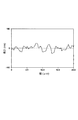
さらされたアルミニウム膜を含有するウエハが冷却後にクリーンルーム雰囲気のカセットに戻されたとき、アルミニウム膜は近似組成Al2O3の自然酸化物に直ちに酸化されることは理解される。アルゴンが約100℃に冷却された後、自然酸化物の厚さが約4.2nmであり、下に横たわるアルミニウムとの接合部がはっきりせず、波状の傾向があり、幾分不鮮明で段階的であると我々は決定した。このようnアルゴン冷却されたアルミニウム膜上で行われた原子間力顕微鏡(AFM)は、10ミクロンの範囲で図5に示した表面プロファイルを生じる。深い溝が明らかである。最高最低粗さの最大値はRmax=101nmであり、表面のRMS粗さはRrms=16.5nmである。電子顕微鏡は、表面の溝間の分離に相当する粒子サイズを示す。更に、個々の粒子の平面は平らでないように見える。 It is understood that when a wafer containing an exposed aluminum film is returned to a clean room atmosphere cassette after cooling, the aluminum film is immediately oxidized to a native oxide of approximate composition Al 2 O 3 . After the argon is cooled to about 100 ° C., the native oxide thickness is about 4.2 nm, the junction with the underlying aluminum is not clear, tends to be wavy, somewhat unclear and graded We decided that. An atomic force microscope (AFM) performed on such an n-argon cooled aluminum film produces the surface profile shown in FIG. 5 in the 10 micron range. Deep grooves are evident. The maximum value of the highest and lowest roughness is R max = 101 nm, and the RMS roughness of the surface is R rms = 16.5 nm. The electron microscope shows a particle size corresponding to the separation between the grooves on the surface. Furthermore, the planes of the individual particles appear not flat.
スパッタされたアルミニウム膜の表面形状は、高純度酸素雰囲気中で冷却を行い、図6の断面図に示されるようにアルミニウム層18の最上部に酸化アルミニウム物114を生じることによって改善することができる。酸化後のみ、フォトリソグラフィに備えて酸化物層114の上に窒化物層22が堆積されている。
The surface shape of the sputtered aluminum film can be improved by cooling in a high-purity oxygen atmosphere to produce an aluminum oxide 114 at the top of the
制御された熱酸化を達成する一実施形態において、図3と図4に示されるように、酸素ガス源120は、酸素ガス(O2)を、ガスバルブ122を通って冷却チャンバに供給する。しかしながら、熱いウエハの高温での純粋な酸素は、厚すぎる酸化物層を生じることがある。従って、一実施形態において、アルゴンのような不活性ガスの実質量を酸素冷却の間にアルゴンガス源106から冷却チャンバ80に供給して、冷却の間の熱転写を促進させる。アルゴン/酸素ガス全圧は約2トールで酸素分圧が約0.01〜0.5トールであるが、約0.1トールの酸素分圧が有益であった。ウエハ32が、冷却の間、約22℃で水冷却ペデスタル32上に支持されるが、冷却は、主に、ペデスタル32への周囲ガスによる対流冷却であると思われる。この全圧における典型的な冷却速度は、約10℃/sである。
In one embodiment to achieve controlled thermal oxidation, the
冷却チャンバ80内の酸素分圧は、ほぼ平坦なパターン形成されていないアルミニウム層18の上面を酸化するとともに図6の断面図に示される酸化アルミニウム層114を形成させる。図5の比較データを生じる同様のアルミニウム堆積条件において、本発明の酸素冷却自然酸化物は、ウエハのアルゴン冷却の後の空気中で形成される従来の自然酸化物の4.2nmに比べて約2nmの厚さを持つことがわかる。アルミニウム層18の部分酸化は、酸化物厚さをアルミニウム層18のフィールド厚さの実質的に10%未満にさせるので、アルミニウム相互接続部の伝導度は実質的に影響されない。更に、酸化物層114と下に横たわるアルミニウム層18との接合部116は、ほぼ単一層全体にはっきりと切り立っている。熱成長した酸化物は、密度が高く、ウエハが100℃未満の周囲空気に戻されたときの酸化を防止すると思われる。周囲空気は、クリーンルームの乾いた空気中でさえ、大部分の窒素と有意量の水蒸気を含有する。双方の成分は、空気酸化に影響することがある。酸素冷却された酸化物のAFMプロファイルを図7に示す。最高最低溝の最大粗さは、Rmax=54.5nmにRMS粗さは、Rrms=11.6nmに低下した。従来のAFMプロファイルと比較すると、深い溝は、除去され、粗さは減少されている。粒子サイズはほぼ同じに見えるが、粒界はアルゴンのみの冷却とより異なっている。
The oxygen partial pressure in the cooling
比較例のアルゴン冷却膜と本発明の酸素冷却膜の数値のデータを表1に示す。シート抵抗はほとんど変化していないが、抵抗率の均一性は著しく改善している。436nmと480nm双方の光学波長の反射率は、酸素冷却において増加している。 Table 1 shows numerical data of the argon cooling film of the comparative example and the oxygen cooling film of the present invention. Although the sheet resistance has hardly changed, the uniformity of resistivity has improved significantly. The reflectivity at both 436 nm and 480 nm optical wavelengths is increased in oxygen cooling.

酸素冷却は、アルミニウムスパッタリングが完了した後であるが、パターン形成された水平の相互接続部を形成するためのエッチング前に、また、アルミニウム酸化に影響するアルミニウム層18上に他の有意な層、例えば、反射防止膜22を堆積させる前に行われなければならない。酸化アルミニウム層114は、絶縁しており、アルミニウム層の上面へのいかなる電気的接触の前にも除去する必要があるが、除去は、自然酸化物の除去ほど難しくない。
Oxygen cooling is after aluminum sputtering is complete, but before etching to form patterned horizontal interconnects, and other significant layers on
熱制御された酸化は、溝112の深さを減少させ、図1と図2のヒロック110を平らにするだけでなく粒子サイズを減少させる。正確なメカニズムは、完全に理解されていない。熱酸化は、おそらく酸化エネルギーによって活性化された初期の粒界に沿って表面拡散を促進させることにより、応力を取り除くと思われる。高度に純粋な酸素の酸化は、水蒸気と高い割合の窒素の双方を含有する空気での酸化より良好な酸化物を生成させる。酸化純度の一基準は、酸化雰囲気の活性成分、即ち、アルゴンやヘリウムのような不活性ガス以外の活性成分が99%の酸素を超えることである。酸素がオゾン(O3)の形であってもよいことは言及すべきである。
Thermally controlled oxidation reduces the depth of the
冷却中の酸素の好ましい分圧は0.1〜0.5トールであるが、プロセス条件によっては酸素分圧のより幅広い許容範囲が0.1〜1トールである。ウエハが熱いときの著しく高い酸素圧は、過度の厚さの酸化物膜を生じやすい。比較的高いアルゴンの分圧、少なくとも酸素の2倍は、全圧が2トールのときに速い冷却速度を可能にする。全圧は、1トールを超える範囲であってもよいが、5トール以下であることが好ましい。アルゴンの量は酸化に対する直接の作用がほとんどなく減少させるか又は除去することさえもできると予想される。しかしながら、アルゴンが減少するにつれて、冷却速度が低下するので、酸化がより高い温度でより長い時間継続し、処理能力も減少する。ヘリウムは、対流冷却ガスとしてアルゴンを置き換えることができる。 The preferred partial pressure of oxygen during cooling is 0.1 to 0.5 Torr, but depending on the process conditions, a wider allowable range of oxygen partial pressure is 0.1 to 1 Torr. The remarkably high oxygen pressure when the wafer is hot tends to produce an excessively thick oxide film. The relatively high argon partial pressure, at least twice oxygen, allows a fast cooling rate when the total pressure is 2 Torr. The total pressure may be in a range exceeding 1 Torr but is preferably 5 Torr or less. It is expected that the amount of argon can be reduced or even eliminated with little direct effect on oxidation. However, as argon decreases, the cooling rate decreases, so the oxidation continues for a longer time at higher temperatures and the throughput is also reduced. Helium can replace argon as a convective cooling gas.
酸素ベースの冷却は、通過チャンバ以外でスパッタチャンバとも関連する搬送チャンバと関連する他のバルブのあるチャンバで行われ得るので、堆積と酸化の間の空気圧が1マイクロトール未満であることが理解される。 It is understood that the air pressure during deposition and oxidation is less than 1 microtorr because oxygen-based cooling can be performed in a chamber with other valves associated with the transfer chamber associated with the sputter chamber in addition to the passage chamber. The
アルミニウム酸化は、酸化が制御され且つスパッタ温度からの冷却によらないように設計されたチャンバ内で行うことができることも理解される。 It is also understood that aluminum oxidation can be performed in a chamber that is designed such that the oxidation is controlled and not dependent on cooling from the sputter temperature.
半導体スパッタリング装置における酸素の使用は、普通ではなく、問題を引き起こす可能性がある。従来、通過チャンバを含むEnduraプラットフォーム上のすべてのチャンバは、プラットフォームに隣接したガス分配パネルに接続された一組の共通のガス源から供給されている。酸素がスパッタチャンバへ又は高真空搬送チャンバへさえアルゴンガスラインに沿って逆に拡散することを防止することは非常に望ましいことである。経験により、アルミニウムスパッタリングチャンバ内に配置される前に高真空搬送チャンバ内での残留酸素にさらされたウエハが、高アスペクト比のバイアを充填するのに厳しいボイドを示すことがわかった。 The use of oxygen in semiconductor sputtering equipment is unusual and can cause problems. Traditionally, all chambers on the Endura platform, including the passage chamber, are supplied from a set of common gas sources connected to a gas distribution panel adjacent to the platform. It is highly desirable to prevent oxygen from diffusing back along the argon gas line into the sputter chamber or even into the high vacuum transfer chamber. Experience has shown that wafers exposed to residual oxygen in a high vacuum transfer chamber before being placed in an aluminum sputtering chamber exhibit severe voids to fill high aspect ratio vias.
プラットフォーム制御のためのソフトウエアは、スパッタチャンバと関連した高真空搬送チャンバと間のスリットバルブが、冷却チャンバと高真空搬送チャンバ間のスリットバルブが開放するときと同じときに開放することを防止するインターロックを含まなければならない。 Software for platform control prevents the slit valve between the high vacuum transfer chamber associated with the sputter chamber from opening at the same time as the slit valve between the cooling chamber and the high vacuum transfer chamber opens. Interlock must be included.
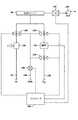
アルゴンが共通の供給源から冷却チャンバやスパッタチャンバへ供給される場合には、冷却チャンバへのアルゴンと酸素の供給のためのバルブは同時に開放されてはならない。即ち、アルゴンと酸素は、それぞれ別々に冷却チャンバへパルスされ、好ましくはアルゴンが最初にパルスされる。冷却の間、冷却チャンバをポンプで排気しない場合には、冷却チャンバへ最初にパルスされるアルゴンと酸素の量が、冷却全体での冷却チャンバ内のアルゴンと酸素の分圧を決定する。冷却チャンバ80へのガス供給システムの図8の概略図で一実施形態を示す。アルゴンは、アルゴンライン132から供給され、その流れは、手動ニードルバルブ134によって定量され、電空バルブ136によって開閉される。同様に、酸素は、酸素供給ライン138から供給され、その流れは、手動ニードルバルブ140によって定量され、電空バルブ142によって開閉される。電空バルブ136、142の出力は、冷却チャンバへ供給される。
If argon is supplied from a common source to the cooling chamber or sputter chamber, the valves for supplying argon and oxygen to the cooling chamber must not be opened simultaneously. That is, argon and oxygen are each pulsed separately into the cooling chamber, preferably argon is pulsed first. If the cooling chamber is not pumped during cooling, the amount of argon and oxygen initially pulsed into the cooling chamber determines the partial pressure of argon and oxygen in the cooling chamber throughout the cooling. One embodiment is shown in the schematic diagram of FIG. 8 of a gas supply system to the cooling
電空(electronic-pneumatic)バルブ136、142は、それぞれ、二つのバルブ段階を持つ。典型的には電気的に駆動するソレノイドによって作動させる第一バルブは、清浄な乾式送気管144からゲートバルブ146を通って供給される清浄な乾燥空気(CDA)の供給を開閉する。開閉された清浄な乾燥空気によって作動させる第二バルブは、電空バルブを通ってアルゴン又は酸素の流れを開閉する。電空バルブ136、142自体は、有効な定量を行わない。コントローラ148は、CDAゲートバルブ146を通って清浄な乾燥空気の供給を開放するために、また、二つの電空バルブ136、142を開閉するために、電気制御シグナルを出す。既知のアルゴンと酸素の圧力で、冷却チャンバに供給されるアルゴン又は酸素の量は、コントローラ148がそれぞれの電空バルブ136、142を開放する時間の量によって決定される。前述したように、コントローラ148は、電空バルブ136、142が同時に開放しないことを確実にしなければならない。また、コントローラ148は、最初に、酸素電空バルブ142を開放する前にアルゴン電空バルブ136を開閉しなければならない。ガス供給のトグリングは、実質的に、酸素がアルゴン空気バルブ136とニードルバルブ134を通ってアルゴン源に向かってスパッタチャンバへ逆に流れることを防止する。アルゴン電空バルブ136は、冷却チャンバ80が酸素パージされるまで再開放してはならない。
Each of the electronic-
酸素分離は、冷却チャンバ専用であり、ゲートバルブ152によってそれに接続されている粗引きポンプ150によって更に改善され得る。粗引きポンプ150は、スパッタリングチャンバ又は高真空搬送チャンバをおおまかにポンプで排気するのには用いられない。コントローラ148は、ゲートバルブ152を閉じ、アルゴンと酸素が冷却チャンバ80に、続いての冷却中に注入される。粗引きポンプは、冷却後冷却チャンバ80を排気する。搬送チャンバと関連付けられたクライオポンプは、冷却チャンバ80を開放されたスロットバルブを通って超高真空へ作動させる。
Oxygen separation can be further improved by a
熱酸化の制御は、図9の概要図に示されるように、酸素ニードルバルブ140をコントローラ148によって電気的に制御されたマスフローコントローラ154で置き換えることによって改善され得る。他の電空バルブ156は、マスフローコントローラ154を分離させることを可能にする。マスフローコントローラは、アルゴンニードルバルブ134に置き換えることができるが、一般に、冷却のためのアルゴン流と圧力は綿密な制御又は調整を必要としない。
Control of thermal oxidation can be improved by replacing the
従って、本発明は、装置の複雑性とコストの増加が小さく且つ処理能力にほとんど影響しないアルミニウムメタライゼーションの品質の著しい改善を可能にする。 Thus, the present invention allows a significant improvement in the quality of aluminum metallization with a small increase in equipment complexity and cost and little impact on throughput.
10…誘電体層、12…導電性特徴部、14…誘電体層、16…バイアホール、18…アルミニウム層、20…上面、22…反射防止コーティング、30…堆積システム、32…ウエハ、34…カセット、36、38…ロードロックチャンバ、40…内部搬送チャンバ、42…内部ロボット、46、48、50、52…処理チャンバ、54、56…通過チャンバ、60…外部ロボット、62…外部搬送チャンバ、64…アルミニウムPVDチャンバ、66…バリヤPVDチャンバ、68、70…処理チャンバ、80…冷却チャンバ、82…真空チャンバ、84、86…ウエハポート、88、90…バルブヘッド、100…ペデスタル、102…冷却装置、104…冷却チャネル、106…アルゴンガス源、108…ガスバルブ、110…ヒロック、112…溝、114…酸化アルミニウム層、116…インタフェース、120…酸素ガス源、122…ガスバルブ、132…アルゴンライン、134…ニードルバルブ、136…電空バルブ、138…酸素ライン、140…ニードルバルブ、142…電空バルブ、144…清浄な乾式送気管、146…ゲートバルブ、148…コントローラ、150…粗引きポンプ、152…ゲートバルブ、154…マスフローコントローラ、156…電空バルブ。
DESCRIPTION OF
Claims (21)
パターン形成されていないアルミニウム層を高温に保持された基板にスパッタ堆積させるステップと;
その後、該パターン形成されていないアルミニウム層を実質的に酸素からなる活性ガスを含有する雰囲気中で部分的に酸化させるステップと;
を含む、前記方法。 A method of depositing aluminum on an interconnect of an integrated circuit comprising:
Sputter depositing an unpatterned aluminum layer on a substrate held at an elevated temperature;
Then partially oxidizing the unpatterned aluminum layer in an atmosphere containing an active gas consisting essentially of oxygen;
Said method.
スパッタリングが、該第一ベース圧未満の第二ベース圧に保持された第二搬送チャンバに隣接したスパッタチャンバ内で行われ、
冷却が、該第一搬送チャンバと該第二搬送チャンバ双方から接近できる通過チャンバ内で行われる、
前記ステップを更に含む、請求項2〜5のいずれか1項に記載の方法。 Loading a substrate from a cassette located adjacent to a first transfer chamber held at a first base pressure, comprising:
Sputtering is performed in a sputter chamber adjacent to a second transfer chamber maintained at a second base pressure less than the first base pressure;
Cooling is performed in a passage chamber accessible from both the first transfer chamber and the second transfer chamber.
The method according to claim 2, further comprising the step.
第一ロボットがその中に配置された第一搬送チャンバと;
複数の基板を運搬し該第一ロボットによって接近できるカセットを含有する該第一搬送チャンバにバルブによって結合されたロードロックチャンバと;
第二ロボットがその中に配置された第二搬送チャンバと;
該第二搬送チャンバにバルブによって結合されたアルミニウムをスパッタするように構成されたスパッタチャンバと;
それぞれのバルブによって該第一搬送チャンバと該第二搬送チャンバに結合され、該一該第一ロボットと該第二ロボットによって接近できる通過チャンバと;
該通過チャンバに制御可能に供給される酸素源と;
を備える、前記プラットフォーム。 A sputtering platform,
A first transfer chamber having a first robot disposed therein;
A load lock chamber coupled by a valve to the first transfer chamber containing a cassette carrying a plurality of substrates and accessible by the first robot;
A second transfer chamber having a second robot disposed therein;
A sputter chamber configured to sputter aluminum coupled by a valve to the second transfer chamber;
A passage chamber coupled to the first transfer chamber and the second transfer chamber by respective valves and accessible by the first robot and the second robot;
An oxygen source that is controllably supplied to the passage chamber;
Comprising the platform.
ロボットを含む搬送チャンバと;
第一バルブによって該搬送チャンバに接続され該ロボットによって接近できる基板にアルミニウムをスパッタするように構成されたスパッタチャンバと;
第二バルブによって該搬送チャンバに接続され、該ロボットによって接近できる、それを冷却するためにその中に該基板を含有する冷却チャンバと;
該冷却チャンバに制御可能に供給される酸素源と;
を備える、前記プラットフォーム。 Sputtering platform:
A transfer chamber containing a robot;
A sputter chamber configured to sputter aluminum onto a substrate connected to the transfer chamber by a first valve and accessible by the robot;
A cooling chamber connected to the transfer chamber by a second valve and accessible by the robot, containing the substrate therein to cool it;
An oxygen source that is controllably supplied to the cooling chamber;
Comprising the platform.
Applications Claiming Priority (1)
| Application Number | Priority Date | Filing Date | Title |
|---|---|---|---|
| US11/843,508 US20090050468A1 (en) | 2007-08-22 | 2007-08-22 | Controlled surface oxidation of aluminum interconnect |
Publications (2)
| Publication Number | Publication Date |
|---|---|
| JP2009065148A true JP2009065148A (en) | 2009-03-26 |
| JP2009065148A5 JP2009065148A5 (en) | 2011-09-29 |
Family
ID=40381134
Family Applications (1)
| Application Number | Title | Priority Date | Filing Date |
|---|---|---|---|
| JP2008212000A Abandoned JP2009065148A (en) | 2007-08-22 | 2008-08-20 | Controlled surface oxidation of aluminum interconnect |
Country Status (5)
| Country | Link |
|---|---|
| US (1) | US20090050468A1 (en) |
| JP (1) | JP2009065148A (en) |
| KR (1) | KR20090020456A (en) |
| CN (1) | CN101373735B (en) |
| TW (1) | TW200909601A (en) |
Cited By (1)
| Publication number | Priority date | Publication date | Assignee | Title |
|---|---|---|---|---|
| JP2019145654A (en) * | 2018-02-20 | 2019-08-29 | エイブリック株式会社 | Semiconductor manufacturing apparatus and method of manufacturing semiconductor device |
Families Citing this family (9)
| Publication number | Priority date | Publication date | Assignee | Title |
|---|---|---|---|---|
| CN102568991B (en) * | 2010-12-17 | 2014-09-24 | 中芯国际集成电路制造(上海)有限公司 | Gas pipeline system of reaction chamber and control method of gas pipeline system |
| CN102586737A (en) * | 2012-03-09 | 2012-07-18 | 上海先进半导体制造股份有限公司 | Physical vapor deposition method of aluminum-copper film |
| US20160013288A1 (en) * | 2014-07-09 | 2016-01-14 | United Microelectronics Corp. | Method of forming a metal gate structure |
| US10559483B2 (en) * | 2016-08-10 | 2020-02-11 | Lam Research Corporation | Platform architecture to improve system productivity |
| US10858727B2 (en) | 2016-08-19 | 2020-12-08 | Applied Materials, Inc. | High density, low stress amorphous carbon film, and process and equipment for its deposition |
| CN108624844B (en) * | 2017-03-17 | 2019-11-12 | 株洲中车时代电气股份有限公司 | A kind of backside of wafer metallic film and preparation method thereof |
| CN108132496B (en) * | 2017-12-28 | 2020-09-18 | 深圳市华星光电技术有限公司 | Metal gate polarizer, manufacturing method thereof, liquid crystal panel and liquid crystal display |
| KR20210032112A (en) * | 2019-09-16 | 2021-03-24 | 삼성전자주식회사 | sputtering system and manufacturing method of magnetic memory device using the same |
| US11674216B2 (en) * | 2019-12-24 | 2023-06-13 | Applied Materials, Inc. | Methods and apparatus for depositing aluminum by physical vapor deposition (PVD) with controlled cooling |
Family Cites Families (15)
| Publication number | Priority date | Publication date | Assignee | Title |
|---|---|---|---|---|
| US4183781A (en) * | 1978-09-25 | 1980-01-15 | International Business Machines Corporation | Stabilization process for aluminum microcircuits which have been reactive-ion etched |
| US4368220A (en) * | 1981-06-30 | 1983-01-11 | International Business Machines Corporation | Passivation of RIE patterned al-based alloy films by etching to remove contaminants and surface oxide followed by oxidation |
| US5186718A (en) * | 1989-05-19 | 1993-02-16 | Applied Materials, Inc. | Staged-vacuum wafer processing system and method |
| US5462892A (en) * | 1992-06-22 | 1995-10-31 | Vlsi Technology, Inc. | Semiconductor processing method for preventing corrosion of metal film connections |
| US6238533B1 (en) * | 1995-08-07 | 2001-05-29 | Applied Materials, Inc. | Integrated PVD system for aluminum hole filling using ionized metal adhesion layer |
| US5935395A (en) * | 1995-11-08 | 1999-08-10 | Mitel Corporation | Substrate processing apparatus with non-evaporable getter pump |
| US6602348B1 (en) * | 1996-09-17 | 2003-08-05 | Applied Materials, Inc. | Substrate cooldown chamber |
| US5913146A (en) * | 1997-03-18 | 1999-06-15 | Lucent Technologies Inc. | Semiconductor device having aluminum contacts or vias and method of manufacture therefor |
| US6177350B1 (en) * | 1998-04-14 | 2001-01-23 | Applied Materials, Inc. | Method for forming a multilayered aluminum-comprising structure on a substrate |
| JP3125745B2 (en) * | 1998-04-30 | 2001-01-22 | 日本電気株式会社 | Method for manufacturing semiconductor device |
| US6287958B1 (en) * | 1999-06-03 | 2001-09-11 | Micron Technology, Inc. | Method of manufacturing a self-aligned etch stop for polycrystalline silicon plugs on a semiconductor device |
| US20030116427A1 (en) * | 2001-08-30 | 2003-06-26 | Applied Materials, Inc. | Self-ionized and inductively-coupled plasma for sputtering and resputtering |
| US6747852B2 (en) * | 2001-08-17 | 2004-06-08 | International Business Machines Corporation | Magnetoresistance sensors with Pt-Mn transverse and longitudinal pinning layers and a decoupling insulation layer |
| US6649537B1 (en) * | 2001-11-19 | 2003-11-18 | Lsi Logic Corporation | Intermittent pulsed oxidation process |
| JPWO2003092084A1 (en) * | 2002-04-23 | 2005-09-02 | 松下電器産業株式会社 | Magnetoresistive element, manufacturing method thereof, magnetic head, magnetic memory and magnetic recording apparatus using the same |
-
2007
- 2007-08-22 US US11/843,508 patent/US20090050468A1/en not_active Abandoned
- 2007-12-12 CN CN2007101987415A patent/CN101373735B/en not_active Expired - Fee Related
- 2007-12-14 TW TW096147994A patent/TW200909601A/en unknown
- 2007-12-21 KR KR1020070135385A patent/KR20090020456A/en not_active Application Discontinuation
-
2008
- 2008-08-20 JP JP2008212000A patent/JP2009065148A/en not_active Abandoned
Cited By (1)
| Publication number | Priority date | Publication date | Assignee | Title |
|---|---|---|---|---|
| JP2019145654A (en) * | 2018-02-20 | 2019-08-29 | エイブリック株式会社 | Semiconductor manufacturing apparatus and method of manufacturing semiconductor device |
Also Published As
| Publication number | Publication date |
|---|---|
| CN101373735A (en) | 2009-02-25 |
| KR20090020456A (en) | 2009-02-26 |
| US20090050468A1 (en) | 2009-02-26 |
| CN101373735B (en) | 2011-07-06 |
| TW200909601A (en) | 2009-03-01 |
Similar Documents
| Publication | Publication Date | Title |
|---|---|---|
| JP2009065148A (en) | Controlled surface oxidation of aluminum interconnect | |
| US7645696B1 (en) | Deposition of thin continuous PVD seed layers having improved adhesion to the barrier layer | |
| US6554914B1 (en) | Passivation of copper in dual damascene metalization | |
| US8017523B1 (en) | Deposition of doped copper seed layers having improved reliability | |
| KR102096143B1 (en) | Ruthenium wiring and manufacturing method thereof | |
| US20060014378A1 (en) | System and method to form improved seed layer | |
| KR102574313B1 (en) | Barrier film deposition and treatment | |
| JP4324617B2 (en) | Sputter deposition method and sputter deposition apparatus | |
| TWI689013B (en) | Cu wiring forming method, semiconductor device manufacturing method, and memory medium | |
| US11908696B2 (en) | Methods and devices for subtractive self-alignment | |
| US6077782A (en) | Method to improve the texture of aluminum metallization | |
| US20190385908A1 (en) | Treatment And Doping Of Barrier Layers | |
| TWI651807B (en) | Cu wiring manufacturing method | |
| KR101800487B1 (en) | Method for forming copper wiring and storage mideum | |
| JP2003249499A (en) | Method for fabricating semiconductor device | |
| WO2014010333A1 (en) | METHOD FOR FORMING Cu WIRING, AND COMPUTER-READABLE MEMORY MEDIUM | |
| US11170998B2 (en) | Method and apparatus for depositing a metal containing layer on a substrate | |
| JP2009182140A (en) | Method of forming thin film, device for plasma deposition and storage medium | |
| US20220364230A1 (en) | Pulsing plasma treatment for film densification | |
| WO2011034092A1 (en) | Method for forming barrier metal film | |
| WO2011034089A1 (en) | Film formation method |
Legal Events
| Date | Code | Title | Description |
|---|---|---|---|
| RD03 | Notification of appointment of power of attorney |
Free format text: JAPANESE INTERMEDIATE CODE: A7423 Effective date: 20101118 |
|
| RD04 | Notification of resignation of power of attorney |
Free format text: JAPANESE INTERMEDIATE CODE: A7424 Effective date: 20101209 |
|
| A521 | Request for written amendment filed |
Free format text: JAPANESE INTERMEDIATE CODE: A523 Effective date: 20110817 |
|
| A621 | Written request for application examination |
Free format text: JAPANESE INTERMEDIATE CODE: A621 Effective date: 20110817 |
|
| A762 | Written abandonment of application |
Free format text: JAPANESE INTERMEDIATE CODE: A762 Effective date: 20120223 |
|
| RD04 | Notification of resignation of power of attorney |
Free format text: JAPANESE INTERMEDIATE CODE: A7424 Effective date: 20120925 |