JP2009062564A - Perovskite type oxide, ferroelectric film and its manufacturing method, ferroelectric element, and liquid discharge apparatus - Google Patents
Perovskite type oxide, ferroelectric film and its manufacturing method, ferroelectric element, and liquid discharge apparatus Download PDFInfo
- Publication number
- JP2009062564A JP2009062564A JP2007229790A JP2007229790A JP2009062564A JP 2009062564 A JP2009062564 A JP 2009062564A JP 2007229790 A JP2007229790 A JP 2007229790A JP 2007229790 A JP2007229790 A JP 2007229790A JP 2009062564 A JP2009062564 A JP 2009062564A
- Authority
- JP
- Japan
- Prior art keywords
- film
- ferroelectric
- ferroelectric film
- substrate
- target
- Prior art date
- Legal status (The legal status is an assumption and is not a legal conclusion. Google has not performed a legal analysis and makes no representation as to the accuracy of the status listed.)
- Withdrawn
Links
Images


Classifications
-
- C—CHEMISTRY; METALLURGY
- C23—COATING METALLIC MATERIAL; COATING MATERIAL WITH METALLIC MATERIAL; CHEMICAL SURFACE TREATMENT; DIFFUSION TREATMENT OF METALLIC MATERIAL; COATING BY VACUUM EVAPORATION, BY SPUTTERING, BY ION IMPLANTATION OR BY CHEMICAL VAPOUR DEPOSITION, IN GENERAL; INHIBITING CORROSION OF METALLIC MATERIAL OR INCRUSTATION IN GENERAL
- C23C—COATING METALLIC MATERIAL; COATING MATERIAL WITH METALLIC MATERIAL; SURFACE TREATMENT OF METALLIC MATERIAL BY DIFFUSION INTO THE SURFACE, BY CHEMICAL CONVERSION OR SUBSTITUTION; COATING BY VACUUM EVAPORATION, BY SPUTTERING, BY ION IMPLANTATION OR BY CHEMICAL VAPOUR DEPOSITION, IN GENERAL
- C23C14/00—Coating by vacuum evaporation, by sputtering or by ion implantation of the coating forming material
- C23C14/22—Coating by vacuum evaporation, by sputtering or by ion implantation of the coating forming material characterised by the process of coating
- C23C14/34—Sputtering
- C23C14/3407—Cathode assembly for sputtering apparatus, e.g. Target
-
- B—PERFORMING OPERATIONS; TRANSPORTING
- B41—PRINTING; LINING MACHINES; TYPEWRITERS; STAMPS
- B41J—TYPEWRITERS; SELECTIVE PRINTING MECHANISMS, i.e. MECHANISMS PRINTING OTHERWISE THAN FROM A FORME; CORRECTION OF TYPOGRAPHICAL ERRORS
- B41J2/00—Typewriters or selective printing mechanisms characterised by the printing or marking process for which they are designed
- B41J2/005—Typewriters or selective printing mechanisms characterised by the printing or marking process for which they are designed characterised by bringing liquid or particles selectively into contact with a printing material
- B41J2/01—Ink jet
- B41J2/135—Nozzles
- B41J2/14—Structure thereof only for on-demand ink jet heads
- B41J2/14201—Structure of print heads with piezoelectric elements
- B41J2/14233—Structure of print heads with piezoelectric elements of film type, deformed by bending and disposed on a diaphragm
-
- B—PERFORMING OPERATIONS; TRANSPORTING
- B41—PRINTING; LINING MACHINES; TYPEWRITERS; STAMPS
- B41J—TYPEWRITERS; SELECTIVE PRINTING MECHANISMS, i.e. MECHANISMS PRINTING OTHERWISE THAN FROM A FORME; CORRECTION OF TYPOGRAPHICAL ERRORS
- B41J2/00—Typewriters or selective printing mechanisms characterised by the printing or marking process for which they are designed
- B41J2/005—Typewriters or selective printing mechanisms characterised by the printing or marking process for which they are designed characterised by bringing liquid or particles selectively into contact with a printing material
- B41J2/01—Ink jet
- B41J2/135—Nozzles
- B41J2/145—Arrangement thereof
- B41J2/155—Arrangement thereof for line printing
-
- C—CHEMISTRY; METALLURGY
- C04—CEMENTS; CONCRETE; ARTIFICIAL STONE; CERAMICS; REFRACTORIES
- C04B—LIME, MAGNESIA; SLAG; CEMENTS; COMPOSITIONS THEREOF, e.g. MORTARS, CONCRETE OR LIKE BUILDING MATERIALS; ARTIFICIAL STONE; CERAMICS; REFRACTORIES; TREATMENT OF NATURAL STONE
- C04B35/00—Shaped ceramic products characterised by their composition; Ceramics compositions; Processing powders of inorganic compounds preparatory to the manufacturing of ceramic products
- C04B35/01—Shaped ceramic products characterised by their composition; Ceramics compositions; Processing powders of inorganic compounds preparatory to the manufacturing of ceramic products based on oxide ceramics
- C04B35/48—Shaped ceramic products characterised by their composition; Ceramics compositions; Processing powders of inorganic compounds preparatory to the manufacturing of ceramic products based on oxide ceramics based on zirconium or hafnium oxides, zirconates, zircon or hafnates
- C04B35/49—Shaped ceramic products characterised by their composition; Ceramics compositions; Processing powders of inorganic compounds preparatory to the manufacturing of ceramic products based on oxide ceramics based on zirconium or hafnium oxides, zirconates, zircon or hafnates containing also titanium oxides or titanates
- C04B35/491—Shaped ceramic products characterised by their composition; Ceramics compositions; Processing powders of inorganic compounds preparatory to the manufacturing of ceramic products based on oxide ceramics based on zirconium or hafnium oxides, zirconates, zircon or hafnates containing also titanium oxides or titanates based on lead zirconates and lead titanates, e.g. PZT
- C04B35/493—Shaped ceramic products characterised by their composition; Ceramics compositions; Processing powders of inorganic compounds preparatory to the manufacturing of ceramic products based on oxide ceramics based on zirconium or hafnium oxides, zirconates, zircon or hafnates containing also titanium oxides or titanates based on lead zirconates and lead titanates, e.g. PZT containing also other lead compounds
-
- C—CHEMISTRY; METALLURGY
- C23—COATING METALLIC MATERIAL; COATING MATERIAL WITH METALLIC MATERIAL; CHEMICAL SURFACE TREATMENT; DIFFUSION TREATMENT OF METALLIC MATERIAL; COATING BY VACUUM EVAPORATION, BY SPUTTERING, BY ION IMPLANTATION OR BY CHEMICAL VAPOUR DEPOSITION, IN GENERAL; INHIBITING CORROSION OF METALLIC MATERIAL OR INCRUSTATION IN GENERAL
- C23C—COATING METALLIC MATERIAL; COATING MATERIAL WITH METALLIC MATERIAL; SURFACE TREATMENT OF METALLIC MATERIAL BY DIFFUSION INTO THE SURFACE, BY CHEMICAL CONVERSION OR SUBSTITUTION; COATING BY VACUUM EVAPORATION, BY SPUTTERING, BY ION IMPLANTATION OR BY CHEMICAL VAPOUR DEPOSITION, IN GENERAL
- C23C14/00—Coating by vacuum evaporation, by sputtering or by ion implantation of the coating forming material
- C23C14/06—Coating by vacuum evaporation, by sputtering or by ion implantation of the coating forming material characterised by the coating material
- C23C14/08—Oxides
- C23C14/088—Oxides of the type ABO3 with A representing alkali, alkaline earth metal or Pb and B representing a refractory or rare earth metal
-
- H—ELECTRICITY
- H10—SEMICONDUCTOR DEVICES; ELECTRIC SOLID-STATE DEVICES NOT OTHERWISE PROVIDED FOR
- H10N—ELECTRIC SOLID-STATE DEVICES NOT OTHERWISE PROVIDED FOR
- H10N30/00—Piezoelectric or electrostrictive devices
- H10N30/01—Manufacture or treatment
- H10N30/07—Forming of piezoelectric or electrostrictive parts or bodies on an electrical element or another base
- H10N30/074—Forming of piezoelectric or electrostrictive parts or bodies on an electrical element or another base by depositing piezoelectric or electrostrictive layers, e.g. aerosol or screen printing
- H10N30/076—Forming of piezoelectric or electrostrictive parts or bodies on an electrical element or another base by depositing piezoelectric or electrostrictive layers, e.g. aerosol or screen printing by vapour phase deposition
-
- H—ELECTRICITY
- H10—SEMICONDUCTOR DEVICES; ELECTRIC SOLID-STATE DEVICES NOT OTHERWISE PROVIDED FOR
- H10N—ELECTRIC SOLID-STATE DEVICES NOT OTHERWISE PROVIDED FOR
- H10N30/00—Piezoelectric or electrostrictive devices
- H10N30/1051—Piezoelectric or electrostrictive devices based on piezoelectric or electrostrictive films or coatings
-
- H—ELECTRICITY
- H10—SEMICONDUCTOR DEVICES; ELECTRIC SOLID-STATE DEVICES NOT OTHERWISE PROVIDED FOR
- H10N—ELECTRIC SOLID-STATE DEVICES NOT OTHERWISE PROVIDED FOR
- H10N30/00—Piezoelectric or electrostrictive devices
- H10N30/80—Constructional details
- H10N30/85—Piezoelectric or electrostrictive active materials
- H10N30/853—Ceramic compositions
- H10N30/8548—Lead based oxides
- H10N30/8554—Lead zirconium titanate based
-
- B—PERFORMING OPERATIONS; TRANSPORTING
- B41—PRINTING; LINING MACHINES; TYPEWRITERS; STAMPS
- B41J—TYPEWRITERS; SELECTIVE PRINTING MECHANISMS, i.e. MECHANISMS PRINTING OTHERWISE THAN FROM A FORME; CORRECTION OF TYPOGRAPHICAL ERRORS
- B41J2202/00—Embodiments of or processes related to ink-jet or thermal heads
- B41J2202/01—Embodiments of or processes related to ink-jet heads
- B41J2202/03—Specific materials used
-
- C—CHEMISTRY; METALLURGY
- C04—CEMENTS; CONCRETE; ARTIFICIAL STONE; CERAMICS; REFRACTORIES
- C04B—LIME, MAGNESIA; SLAG; CEMENTS; COMPOSITIONS THEREOF, e.g. MORTARS, CONCRETE OR LIKE BUILDING MATERIALS; ARTIFICIAL STONE; CERAMICS; REFRACTORIES; TREATMENT OF NATURAL STONE
- C04B2235/00—Aspects relating to ceramic starting mixtures or sintered ceramic products
- C04B2235/02—Composition of constituents of the starting material or of secondary phases of the final product
- C04B2235/30—Constituents and secondary phases not being of a fibrous nature
- C04B2235/32—Metal oxides, mixed metal oxides, or oxide-forming salts thereof, e.g. carbonates, nitrates, (oxy)hydroxides, chlorides
- C04B2235/3224—Rare earth oxide or oxide forming salts thereof, e.g. scandium oxide
- C04B2235/3227—Lanthanum oxide or oxide-forming salts thereof
-
- C—CHEMISTRY; METALLURGY
- C04—CEMENTS; CONCRETE; ARTIFICIAL STONE; CERAMICS; REFRACTORIES
- C04B—LIME, MAGNESIA; SLAG; CEMENTS; COMPOSITIONS THEREOF, e.g. MORTARS, CONCRETE OR LIKE BUILDING MATERIALS; ARTIFICIAL STONE; CERAMICS; REFRACTORIES; TREATMENT OF NATURAL STONE
- C04B2235/00—Aspects relating to ceramic starting mixtures or sintered ceramic products
- C04B2235/02—Composition of constituents of the starting material or of secondary phases of the final product
- C04B2235/30—Constituents and secondary phases not being of a fibrous nature
- C04B2235/32—Metal oxides, mixed metal oxides, or oxide-forming salts thereof, e.g. carbonates, nitrates, (oxy)hydroxides, chlorides
- C04B2235/3231—Refractory metal oxides, their mixed metal oxides, or oxide-forming salts thereof
- C04B2235/3251—Niobium oxides, niobates, tantalum oxides, tantalates, or oxide-forming salts thereof
-
- C—CHEMISTRY; METALLURGY
- C04—CEMENTS; CONCRETE; ARTIFICIAL STONE; CERAMICS; REFRACTORIES
- C04B—LIME, MAGNESIA; SLAG; CEMENTS; COMPOSITIONS THEREOF, e.g. MORTARS, CONCRETE OR LIKE BUILDING MATERIALS; ARTIFICIAL STONE; CERAMICS; REFRACTORIES; TREATMENT OF NATURAL STONE
- C04B2235/00—Aspects relating to ceramic starting mixtures or sintered ceramic products
- C04B2235/02—Composition of constituents of the starting material or of secondary phases of the final product
- C04B2235/30—Constituents and secondary phases not being of a fibrous nature
- C04B2235/32—Metal oxides, mixed metal oxides, or oxide-forming salts thereof, e.g. carbonates, nitrates, (oxy)hydroxides, chlorides
- C04B2235/3231—Refractory metal oxides, their mixed metal oxides, or oxide-forming salts thereof
- C04B2235/3258—Tungsten oxides, tungstates, or oxide-forming salts thereof
-
- C—CHEMISTRY; METALLURGY
- C04—CEMENTS; CONCRETE; ARTIFICIAL STONE; CERAMICS; REFRACTORIES
- C04B—LIME, MAGNESIA; SLAG; CEMENTS; COMPOSITIONS THEREOF, e.g. MORTARS, CONCRETE OR LIKE BUILDING MATERIALS; ARTIFICIAL STONE; CERAMICS; REFRACTORIES; TREATMENT OF NATURAL STONE
- C04B2235/00—Aspects relating to ceramic starting mixtures or sintered ceramic products
- C04B2235/02—Composition of constituents of the starting material or of secondary phases of the final product
- C04B2235/30—Constituents and secondary phases not being of a fibrous nature
- C04B2235/32—Metal oxides, mixed metal oxides, or oxide-forming salts thereof, e.g. carbonates, nitrates, (oxy)hydroxides, chlorides
- C04B2235/3298—Bismuth oxides, bismuthates or oxide forming salts thereof, e.g. zinc bismuthate
-
- C—CHEMISTRY; METALLURGY
- C04—CEMENTS; CONCRETE; ARTIFICIAL STONE; CERAMICS; REFRACTORIES
- C04B—LIME, MAGNESIA; SLAG; CEMENTS; COMPOSITIONS THEREOF, e.g. MORTARS, CONCRETE OR LIKE BUILDING MATERIALS; ARTIFICIAL STONE; CERAMICS; REFRACTORIES; TREATMENT OF NATURAL STONE
- C04B2235/00—Aspects relating to ceramic starting mixtures or sintered ceramic products
- C04B2235/70—Aspects relating to sintered or melt-casted ceramic products
- C04B2235/74—Physical characteristics
- C04B2235/76—Crystal structural characteristics, e.g. symmetry
- C04B2235/768—Perovskite structure ABO3
Abstract
Description
本発明は、PZT系のペロブスカイト型酸化物、これを含む強誘電体膜とその製造方法、この強誘電体膜を用いた強誘電体素子及び液体吐出装置に関するものである。 The present invention relates to a PZT-based perovskite oxide, a ferroelectric film including the same, a method for manufacturing the same, a ferroelectric element using the ferroelectric film, and a liquid discharge apparatus.
電界印加強度の増減に伴って伸縮する圧電性を有する圧電体と、圧電体に対して電界を印加する電極とを備えた圧電素子が、インクジェット式記録ヘッドに搭載される圧電アクチュエータ等の用途に使用されている。圧電材料としては、ジルコンチタン酸鉛(PZT)等のペロブスカイト型酸化物が広く用いられている。かかる圧電材料は電界無印加時において自発分極性を有する強誘電体である。 A piezoelectric element including a piezoelectric body having piezoelectricity that expands and contracts as the electric field application intensity increases and decreases, and an electrode that applies an electric field to the piezoelectric body is used for applications such as a piezoelectric actuator mounted on an ink jet recording head. in use. As the piezoelectric material, perovskite oxides such as lead zirconate titanate (PZT) are widely used. Such a piezoelectric material is a ferroelectric having spontaneous polarization when no electric field is applied.
被置換イオンの価数よりも高い価数を有する各種ドナイオンを添加したPZTでは、真性PZTよりも強誘電性能等の特性が向上することが1960年代より知られている。AサイトのPb2+を置換するドナイオンとして、Bi3+,及びLa3+等の各種ランタノイドのカチオンが知られている。BサイトのZr4+及び/又はTi4+を置換するドナイオンとして、V5+,Nb5+,Ta5+,Sb5+,Mo6+,及びW6+等が知られている。 It has been known since the 1960s that PZT to which various donor ions having a valence higher than that of a substituted ion are added has improved properties such as ferroelectric performance compared to intrinsic PZT. As donor ions for substituting Pb 2+ at the A site, various lanthanoid cations such as Bi 3+ and La 3+ are known. V 5+ , Nb 5+ , Ta 5+ , Sb 5+ , Mo 6+ , W 6+ and the like are known as donor ions for substituting Zr 4+ and / or Ti 4+ on the B site.
強誘電体は古くは、所望組成の構成元素を含む複数種の酸化物粉末を混合し、得られた混合粉末を成型及び焼成する、あるいは所望組成の構成元素を含む複数種の酸化物粉末を有機バインダに分散させたものを基板に塗布し焼成するなどの方法により製造されていた。かかる方法では、強誘電体は600℃以上、通常1000℃以上の焼成工程を経て、製造されていた。かかる方法では、高温の熱平衡状態で製造を行うため、本来価数が合わない添加物を高濃度ドープすることはできなかった。 In the past, ferroelectrics mixed multiple types of oxide powders containing constituent elements of the desired composition, and molded and fired the resulting mixed powder, or multiple types of oxide powders containing the constituent elements of the desired composition. A material dispersed in an organic binder is applied to a substrate and baked. In such a method, the ferroelectric has been manufactured through a baking step of 600 ° C. or higher, usually 1000 ° C. or higher. In such a method, since the production is carried out in a high temperature thermal equilibrium state, it was impossible to dope a high concentration of an additive whose valence is not suitable.
非特許文献1には、PZTバルクセラミックスに対する各種ドナイオンの添加についての研究が記載されている。図15に、非特許文献1のFig.14を示す。この図は、ドナイオンの添加量と誘電率との関係を示す図である。この図には、1.0モル%程度(図では0.5wt%程度に相当)で最も特性が良くなり、それ以上添加すると特性が低下することが示されている。これは、価数が合わないが故に固溶しないドナイオンが粒界等に偏析して、特性を低下させるためであると考えられる。
Non-Patent
近年、特許文献1〜4には、Aサイトに非特許文献1よりも高濃度のドナイオンをドープした強誘電体が開示されている。
In recent years,
特許文献1には、Aサイトに0モル%超100モル%未満のBiをドープし、Bサイトに5モル%以上40モル%以下のNb又はTaをドープしたPZT系の強誘電体膜が開示されている(請求項1)。この強誘電体膜はゾルゲル法によって成膜されている。ゾルゲル法は熱平衡プロセスであり、特許文献1では、焼結を促進して熱平衡状態を得るために、焼結助剤としてSiを添加することが必須となっている(段落[0108]等参照)。
特許文献1には、AサイトにBiをドープすることにより酸素欠損が低減されて、電流リークが低減されることが記載されている(段落[0040]等参照)。特許文献1にはまた、BiとNb又はTaとの添加量が増大するにつれて、分極−電界ヒステリシスの角形性が向上し、分極−電界ヒステリシスが良好となることが記載されている(段落[0114]等参照)。
特許文献2には、0.01〜10重量%のBi2O3と0.01〜10重量%のGeO2とを含むPZT系バルク焼結体が開示されている。特許文献3には、0.01〜10重量%のBi2O3と0.01〜10重量%のV2O5とを含むPZT系バルク焼結体が開示されている。特許文献2及び3には、焼結助剤としてGe又はVを添加することで、比較的低温で焼結できることが記載されている。
特許文献4には、価数を合わせるために、高価数のドナイオンであるBiと、低価数のアクセプタイオンであるSc又はInとを共ドープしたPZT系のバルク焼結体が開示されている。
特許文献1〜3に記載の強誘電体では、焼結を促進して熱平衡状態を得るために、焼結助剤としてSi,Ge,又はVを添加することが必須となっている。かかる焼結助剤を添加すると強誘電特性が低下するため、特許文献1〜3に記載の方法では、Aサイトのドナイオン添加の効果を充分に引き出すことができない。
In the ferroelectrics described in
なお、特許文献3で用いられているVはBサイトのドナイオンであるが、Nb及びTaよりもイオン半径が小さく、Vのドナイオンとしての効果はNb及びTaより小さいと考えられる。また、V2O5は毒性も強く、使用を避けることが好ましい。
V used in
特許文献4に記載の強誘電体では、価数を合わせるために、高価数のドナイオンと低価数のアクセプタイオンとを共ドープしている。しかしながら、低価数のアクセプタイオンは強誘電特性を下げることが知られており、アクセプタイオンを共ドープする系ではドナイオン添加の効果を充分に引き出すことができない。 In the ferroelectric described in Patent Document 4, an expensive donor ion and a low-valence acceptor ion are co-doped to match the valence. However, it is known that acceptor ions having a low valence will lower the ferroelectric properties, and the effect of adding donor ions cannot be sufficiently obtained in a system in which acceptor ions are co-doped.
電子機器の小型軽量化・高機能化に伴い、これに搭載される圧電素子においても小型軽量化・高機能化が進められるようになってきている。例えば、インクジェット式記録ヘッドでは、高画質化のために、圧電素子の高密度化が検討されており、それに伴って圧電素子の薄型化が検討されている。強誘電体の形態としては、薄膜が好ましい。 As electronic devices become smaller, lighter and more functional, piezoelectric elements mounted on the electronic devices are becoming smaller, lighter and more functional. For example, in an ink jet recording head, increasing the density of piezoelectric elements is being studied in order to improve image quality, and accordingly, reducing the thickness of piezoelectric elements is being studied. A thin film is preferable as the form of the ferroelectric.
特許文献2〜4ではバルク焼結体が対象とされている。特許文献1ではゾルゲル法による強誘電体膜の成膜が記載されている。ゾルゲル法では、膜厚を厚くするとクラックが入るため、1μm以下の薄膜しか成膜することができない。強誘電体メモリ等の用途ではかかる薄膜でもよいが、圧電素子では充分な変位が得られないため、強誘電体膜の膜厚は3μm以上が好ましい。薄膜の積層を繰り返すことで膜厚を厚くすることはできなくはないが、実用的ではない。また、ゾルゲル法ではPb欠損が起こりやすい。Pb欠損が起こると、強誘電体性能が低下する傾向にあり、好ましくない。
In
本発明は上記事情に鑑みてなされたものであり、焼結助剤やアクセプタイオンを添加することなく、Aサイトに5モル%以上のドナイオンを添加することが可能なPZT系のペロブスカイト型酸化物の製造方法を提供することを目的とするものである。
本発明はまた、上記製造方法により、Aサイトに5モル%以上のドナイオンが添加され、強誘電性能に優れたPZT系のペロブスカイト型酸化物を提供することを目的とするものである。
本発明はまた、Aサイト欠損がなく、Aサイトに5モル%以上のドナイオンが添加され、強誘電性能に優れたPZT系のペロブスカイト型酸化物を提供することを目的とするものである。
本発明はまた、Aサイトに5モル%以上のドナイオンが添加され、強誘電性能に優れたPZT系のペロブスカイト型酸化物を含み、3.0μm以上の膜厚を有する強誘電体膜を提供することを目的とするものである。
The present invention has been made in view of the above circumstances, and a PZT-based perovskite oxide in which 5 mol% or more of donor ions can be added to the A site without adding a sintering aid or acceptor ions. An object of the present invention is to provide a manufacturing method.
Another object of the present invention is to provide a PZT-based perovskite oxide having excellent ferroelectric performance in which 5 mol% or more of donor ions are added to the A site by the above production method.
Another object of the present invention is to provide a PZT-based perovskite oxide that has no A-site deficiency and is doped with 5 mol% or more of donor ions at the A-site and has excellent ferroelectric performance.
The present invention also provides a ferroelectric film having a thickness of 3.0 μm or more, including a PZT-based perovskite oxide having a ferroelectric property of 5 mol% or more added to the A site and having excellent ferroelectric performance. It is for the purpose.
本発明のペロブスカイト型酸化物は、下記式(P)で表されることを特徴とするものである。
(Pb1−x+δMx)(ZryTi1−y)Oz・・・(P)
(式中、MはBi及びランタニド元素(=元素番号57〜71の元素(La〜Lu))からなる群より選ばれた少なくとも1種の元素である。
0.05≦x≦0.4。
0<y≦0.7。
δ=0及びz=3が標準であるが、これらの値はペロブスカイト構造を取り得る範囲内で基準値からずれてもよい。)
The perovskite oxide of the present invention is represented by the following formula (P).
(Pb 1-x + δM x ) (Zr y Ti 1-y ) O z (P)
(In the formula, M is at least one element selected from the group consisting of Bi and lanthanide elements (= elements of element numbers 57 to 71 (La to Lu)).
0.05 ≦ x ≦ 0.4.
0 <y ≦ 0.7.
Although δ = 0 and z = 3 are standard, these values may deviate from the reference value within a range where a perovskite structure can be taken. )
本発明のペロブスカイト型酸化物において、MがBiであることが好ましい。この場合、0.05≦x≦0.25であることが好ましい。 In the perovskite oxide of the present invention, M is preferably Bi. In this case, it is preferable that 0.05 ≦ x ≦ 0.25.
本発明では、0<δ≦0.2であるAサイト元素がリッチな組成のペロブスカイト型酸化物を提供することができる。
本発明では、Si,Ge,及びVを実質的に含まないペロブスカイト型酸化物を提供することができる。「Si,Ge,及びVを実質的に含まない」とは、ペロブスカイト型酸化物の表面(例えば、ペロブスカイト型酸化物膜である場合は膜表面)からの蛍光X線測定により検出される各元素の濃度が、Siの場合は0.1wt%未満,Ge及びVの場合は0.01%未満であることと定義する。
In the present invention, it is possible to provide a perovskite oxide having a composition rich in the A site element satisfying 0 <δ ≦ 0.2.
The present invention can provide a perovskite oxide substantially free of Si, Ge, and V. “Substantially free of Si, Ge, and V” means each element detected by fluorescent X-ray measurement from the surface of the perovskite oxide (for example, the film surface in the case of a perovskite oxide film). The concentration of Si is defined to be less than 0.1 wt% in the case of Si and less than 0.01% in the case of Ge and V.
本発明の強誘電体膜は、上記の本発明のペロブスカイト型酸化物を含むことを特徴とするものである。
本発明では、バイポーラ分極−電界曲線において、正電界側の抗電界をEc1とし、負電界側の抗電界をEc2としたとき、(Ec1+Ec2)/(Ec1−Ec2)×100(%)の値が25%以下である強誘電体膜を提供することができる。
本発明では、多数の柱状結晶からなる膜構造を有する強誘電体膜を提供することができる。
本発明では、3.0μm以上の膜厚を有する強誘電体膜を提供することができる。
The ferroelectric film of the present invention includes the perovskite oxide of the present invention.
In the present invention, when the coercive electric field on the positive electric field side is Ec1 and the coercive electric field on the negative electric field side is Ec2 in the bipolar polarization-electric field curve, the value of (Ec1 + Ec2) / (Ec1−Ec2) × 100 (%) is A ferroelectric film that is 25% or less can be provided.
The present invention can provide a ferroelectric film having a film structure composed of a large number of columnar crystals.
In the present invention, a ferroelectric film having a film thickness of 3.0 μm or more can be provided.
本発明の強誘電体膜は、非熱平衡プロセスにより成膜することができる。本発明の強誘電体膜の好適な成膜方法としては、スパッタ法が挙げられる。 The ferroelectric film of the present invention can be formed by a non-thermal equilibrium process. As a suitable film formation method for the ferroelectric film of the present invention, a sputtering method may be mentioned.
前記スパッタ法は、成膜する該強誘電体膜の膜組成に応じた組成のターゲットと基板とを対向配置させ、下記式(1)及び(2)を充足する成膜条件、又は下記式(3)及び(4)を充足する成膜条件で、基板上に成膜を行うものであることが好ましい。
400≦Ts(℃)≦500・・・(1)、
30≦D(mm)≦80・・・(2)、
500≦Ts(℃)≦600・・・(3)、
30≦D(mm)≦100・・・(4)
(式(1)〜(4)中、Ts(℃)は成膜温度、D(mm)は基板とターゲットとの離間距離である。)
In the sputtering method, a target having a composition corresponding to the film composition of the ferroelectric film to be deposited and a substrate are arranged to face each other, and film formation conditions satisfying the following formulas (1) and (2), or the following formula ( It is preferable that the film is formed on the substrate under the film forming conditions satisfying 3) and (4).
400 ≦ Ts (° C.) ≦ 500 (1),
30 ≦ D (mm) ≦ 80 (2),
500 ≦ Ts (° C.) ≦ 600 (3),
30 ≦ D (mm) ≦ 100 (4)
(In the formulas (1) to (4), Ts (° C.) is the deposition temperature, and D (mm) is the distance between the substrate and the target.)
本明細書において、「成膜温度Ts(℃)」は、成膜を行う基板の中心温度を意味するものとする。
本明細書において、「基板―ターゲット間距離」とは、ターゲット側の基板面における中心と、ターゲットとを、ターゲットに対して垂直となるように結んだ距離と定義する。複数のターゲットを用いて同時に成膜を行う場合は、それぞれの基板―ターゲット間距離の平均値とする。
In this specification, “film formation temperature Ts (° C.)” means the center temperature of the substrate on which film formation is performed.
In this specification, the “substrate-target distance” is defined as a distance obtained by connecting the center of the substrate surface on the target side and the target so as to be perpendicular to the target. When film formation is performed simultaneously using a plurality of targets, the average value of the distance between each substrate and the target is used.
本発明の強誘電体素子は、上記の本発明の強誘電体膜と、該強誘電体膜に対して電界を印加する電極とを備えたことを特徴とするものである。
本発明の液体吐出装置は、上記の本発明の強誘電体素子からなる圧電素子と、
液体が貯留される液体貯留室及び該液体貯留室から外部に前記液体が吐出される液体吐出口を有する液体貯留吐出部材とを備えたことを特徴とするものである。
A ferroelectric element of the present invention includes the ferroelectric film of the present invention described above and an electrode for applying an electric field to the ferroelectric film.
The liquid ejection device of the present invention includes a piezoelectric element comprising the ferroelectric element of the present invention,
A liquid storage chamber in which liquid is stored, and a liquid storage and discharge member having a liquid discharge port through which the liquid is discharged from the liquid storage chamber are provided.
本発明は、PZT系のペロブスカイト型酸化物において、焼結助剤やアクセプタイオンを添加することなく、Aサイトに5〜40モル%のドナイオンを添加することを実現したものである。本発明のペロブスカイト型酸化物は、Aサイトに5〜40モル%の高濃度のドナイオンが添加されたものであるので、強誘電性能(圧電性能)に優れている。本発明のペロブスカイト型酸化物では、焼結助剤やアクセプタイオンを添加することなく、Aサイトにかかる高濃度のドナイオンを添加できるので、焼結助剤やアクセプタイオンによる強誘電性能の低下が抑制され、ドナイオンの添加による強誘電性能の向上が最大限引き出される。 In the PZT-based perovskite oxide, the present invention realizes addition of 5 to 40 mol% of donor ions at the A site without adding a sintering aid or acceptor ions. The perovskite oxide of the present invention is excellent in ferroelectric performance (piezoelectric performance) because a high concentration of 5-40 mol% of donor ions is added to the A site. In the perovskite type oxide of the present invention, since a high concentration of donor ions at the A site can be added without adding a sintering aid or acceptor ion, a decrease in ferroelectric performance due to the sintering aid or acceptor ion is suppressed. Therefore, the improvement of the ferroelectric performance due to the addition of dona ions is maximized.
「ペロブスカイト型酸化物、強誘電体膜」
本発明者は、スパッタ法等の非熱平衡プロセスにより成膜を行うことにより、焼結助剤やアクセプタイオンを添加することなく、ジルコンチタン酸鉛(PZT)のAサイトに5モル%以上のドナイオンを添加できることを見出した。本発明者は具体的には、PZTのAサイトに5〜40モル%のドナイオンを添加できることを見出した。
"Perovskite oxide, ferroelectric film"
The present inventor has formed a film by a non-thermal equilibrium process such as a sputtering method, so that 5 mol% or more of donor ions are added to the A site of lead zirconate titanate (PZT) without adding a sintering aid or an acceptor ion. It was found that can be added. Specifically, the present inventor has found that 5 to 40 mol% of donor ions can be added to the A site of PZT.
すなわち、本発明のペロブスカイト型酸化物は、下記式(P)で表されることを特徴とするものである。
(Pb1−x+δMx)(ZryTi1−y)Oz・・・(P)
(式中、MはBi及びランタニド元素からなる群より選ばれた少なくとも1種の元素である。
0.05≦x≦0.4。
0<y≦0.7。
δ=0及びz=3が標準であるが、これらの値はペロブスカイト構造を取り得る範囲内で基準値からずれてもよい。)
That is, the perovskite oxide of the present invention is represented by the following formula (P).
(Pb 1-x + δM x ) (Zr y Ti 1-y ) O z (P)
(In the formula, M is at least one element selected from the group consisting of Bi and lanthanide elements.
0.05 ≦ x ≦ 0.4.
0 <y ≦ 0.7.
Although δ = 0 and z = 3 are standard, these values may deviate from the reference value within a range where a perovskite structure can be taken. )
本発明の強誘電体膜は、上記の本発明のペロブスカイト型酸化物を含むことを特徴とするものである。
本発明では、上記の本発明のペロブスカイト型酸化物を主成分とする強誘電体膜を提供することができる。本明細書において、「主成分」は80質量%以上の成分と定義する。
The ferroelectric film of the present invention includes the perovskite oxide of the present invention.
The present invention can provide a ferroelectric film containing the perovskite oxide of the present invention as a main component. In the present specification, the “main component” is defined as a component of 80% by mass or more.
特許文献1〜3では、焼結助剤としてSi,Ge,又はVを添加することが必須であるが、本発明ではSi,Ge,及びVを実質的に含まないペロブスカイト型酸化物を提供することができる。焼結助剤としてはSnも知られているが、本発明ではSnを実質的に含まないペロブスカイト型酸化物を提供することもできる。
In
特許文献4では、ドナイオンを高濃度ドープするために、アクセプタイオンであるSc又はInを共ドープしているが、本発明ではかかるアクセプタイオンを実質的に含まないペロブスカイト型酸化物を提供することができる。 In Patent Document 4, Sc or In, which is an acceptor ion, is co-doped in order to dope a donor ion at a high concentration, but the present invention provides a perovskite oxide that does not substantially contain such acceptor ion. it can.
焼結助剤やアクセプタイオンによって強誘電性能の低下が抑制することが知られている。本発明では焼結助剤やアクセプタイオンを必須としないので、焼結助剤やアクセプタイオンによる強誘電性能の低下が抑制され、ドナイオンの添加による強誘電性能の向上が最大限引き出される。なお、本発明では、焼結助剤やアクセプタイオンを必須としないが、特性に支障のない限り、これらを添加することは差し支えない。 It is known that a decrease in ferroelectric performance is suppressed by a sintering aid or acceptor ions. In the present invention, since the sintering aid and acceptor ions are not essential, the deterioration of the ferroelectric performance due to the sintering aid and acceptor ions is suppressed, and the improvement of the ferroelectric performance due to the addition of donor ions is maximized. In the present invention, sintering aids and acceptor ions are not essential, but they can be added as long as the characteristics are not hindered.
本発明のペロブスカイト型酸化物は、Aサイトに5〜40モル%のドナイオンが添加されたものであるので、真性PZTあるいはPZTのBサイトにドナイオンが添加されたものに比較して、Pb量が少なく、環境に対する負荷が少なく、好ましい。 Since the perovskite oxide of the present invention has 5-40 mol% of donor ions added to the A site, the amount of Pb is lower than that of intrinsic PZT or PZT added with donor ions. Less, less burden on the environment, preferable.
本発明者は、PZTのBサイトにドナイオンであるNb,Ta,又はWを添加したPZT膜では、バイポーラ分極-電界曲線(PE曲線)が正電界側に偏った非対称ヒステリシスを示すのに対して、Aサイトにドナイオンを添加した本発明のペロブスカイト型酸化物を含む強誘電体膜では、PE曲線の非対称ヒステリシスが緩和されて、対称ヒステリシスに近くなることを見出している。PEヒステリシスが非対称であることは、負電界側の抗電界Ec1の絶対値と正電界側の抗電界Ec2とが異なること(|Ec1|≠Ec2)により定義される。 In the PZT film in which Nb, Ta, or W, which is a donor ion, is added to the B site of PZT, the present inventor shows asymmetric hysteresis in which the bipolar polarization-electric field curve (PE curve) is biased to the positive electric field side. In the ferroelectric film containing the perovskite oxide of the present invention in which donor ions are added to the A site, it has been found that the asymmetric hysteresis of the PE curve is relaxed and becomes close to symmetrical hysteresis. That the PE hysteresis is asymmetric is defined by the fact that the absolute value of the coercive electric field Ec1 on the negative electric field side is different from the coercive electric field Ec2 on the positive electric field side (| Ec1 | ≠ Ec2).
通常、強誘電体膜は、下部電極と強誘電体膜と上部電極とが順次積み重ねられた強誘電体素子の形態で使用され、下部電極と上部電極とのうち、一方の電極を印加電圧が0Vに固定されるグランド電極とし、他方の電極を印加電圧が変動されるアドレス電極として、駆動される。駆動しやすいことから、通常は下部電極をグランド電極とし、上部電極をアドレス電極として、駆動が行われる。「強誘電体膜に負電界が印加されている状態」とは、アドレス電極に負電圧を印加した状態を意味する。同様に、「強誘電体膜に正電界が印加されている状態」とは、アドレス電極に正電圧を印加した状態を意味する。 Usually, the ferroelectric film is used in the form of a ferroelectric element in which a lower electrode, a ferroelectric film, and an upper electrode are sequentially stacked, and an applied voltage is applied to one of the lower electrode and the upper electrode. The ground electrode is fixed at 0V, and the other electrode is driven as an address electrode whose applied voltage is varied. Since it is easy to drive, the driving is usually performed using the lower electrode as a ground electrode and the upper electrode as an address electrode. The “state in which a negative electric field is applied to the ferroelectric film” means a state in which a negative voltage is applied to the address electrodes. Similarly, “a state where a positive electric field is applied to the ferroelectric film” means a state where a positive voltage is applied to the address electrodes.
正電界側に偏ったPE非対称ヒステリシスを有する強誘電体膜では、正電界を印加した場合は分極されにくく、負電界を印加した場合は分極されやすい。この場合、正電界印加では圧電特性が出にくく、負電界印加で圧電特性が出やすい。負電界を印加するには、上部電極の駆動ドライバICを負電圧用にする必要があるが、負電圧用は汎用されておらず、ICの開発コストがかかってしまう。下部電極をパターニングしてアドレス電極とし上部電極をグランド電極とすれば、汎用の正電圧用の駆動ドライバICを用いることができるが、製造プロセスが複雑になり、好ましくない。 A ferroelectric film having PE asymmetric hysteresis biased toward the positive electric field side is not easily polarized when a positive electric field is applied, and is easily polarized when a negative electric field is applied. In this case, piezoelectric characteristics are difficult to be obtained when a positive electric field is applied, and piezoelectric characteristics are likely to be obtained when a negative electric field is applied. In order to apply a negative electric field, the drive driver IC for the upper electrode needs to be used for a negative voltage, but the negative voltage is not widely used, and the development cost of the IC is increased. If the lower electrode is patterned to be an address electrode and the upper electrode is a ground electrode, a general-purpose positive voltage driver IC can be used, but the manufacturing process becomes complicated, which is not preferable.
本発明の強誘電体膜では、PE曲線が対称ヒステリシスに近くなるため、駆動の観点から、好ましい。
PE曲線の非対称ヒステリシスのレベルは、(Ec1+Ec2)/(Ec1−Ec2)×100(%)の値により評価でき、この数値が大きい程、PEヒステリシスの非対称性が大きいことを示す。本発明では、(Ec1+Ec2)/(Ec1−Ec2)×100(%)の値が25%以下である強誘電体膜を提供することができる(後記実施例1、図8を参照)。
The ferroelectric film of the present invention is preferable from the viewpoint of driving because the PE curve is close to symmetrical hysteresis.
The level of asymmetric hysteresis of the PE curve can be evaluated by the value of (Ec1 + Ec2) / (Ec1−Ec2) × 100 (%), and the larger this value, the greater the asymmetry of the PE hysteresis. In the present invention, a ferroelectric film having a value of (Ec1 + Ec2) / (Ec1−Ec2) × 100 (%) of 25% or less can be provided (see Example 1 and FIG. 8 described later).
本発明のペロブスカイト型酸化物において、式(P)中のMがBiであることが好ましい。本発明者は、MがBiのとき、PE曲線が対称ヒステリシスに近く、かつ、強誘電性能に優れた強誘電体膜が得られることを見出している。「背景技術」の項において、特許文献1には、BiとNb又はTaとを共ドープすることにより、PEヒステリシスの角形性が向上し、PEヒステリシスが良好となることが記載されていることを述べたが、本発明者はAサイトドナイオンであるBiとBサイトドナイオンであるNb又はTaとを共ドープする特許文献1よりも、Aサイトドナイオンのみをドープする本発明の系の方が、PEヒステリシスの対称性が良いことを見出している(後記実施例1、図7A及び図7Bを参照)。
In the perovskite oxide of the present invention, M in the formula (P) is preferably Bi. The inventor has found that when M is Bi, a ferroelectric film having a PE curve close to symmetrical hysteresis and excellent in ferroelectric performance can be obtained. In the section “Background Art”,
本発明のペロブスカイト型酸化物は特性に支障のない限り、異相を含むものであってもよいが、本発明者は、MがBiであるとき、XRD測定から、少なくとも0.05≦x≦0.30の範囲において単相構造のペロブスカイト型酸化物が得られることを確認している。 The perovskite oxide of the present invention may contain a heterogeneous phase as long as there is no problem in the characteristics. However, when M is Bi, the present inventor has found that at least 0.05 ≦ x ≦ 0 from XRD measurement. It is confirmed that a perovskite oxide having a single phase structure can be obtained in the range of .30.
本発明者はまた、MがBiであるとき、0.05≦x≦0.25の範囲おいて、特に誘電率ε及び最大分極値Pmax等が高く、強誘電性能に優れたペロブスカイト型酸化物が得られることを見出している(後記実施例1、図6を参照)。したがって、MがBiであるとき、強誘電性能の観点から、0.05≦x≦0.25であることが好ましい。この範囲より高濃度ドープの0.25≦x≦0.40の範囲は、Pb量低減による環境に対する負荷低減効果の観点から、好ましい。 The present inventor has also found that when M is Bi, a perovskite oxide having a high dielectric constant ε, a maximum polarization value Pmax, etc. and excellent ferroelectric performance in a range of 0.05 ≦ x ≦ 0.25. (See Example 1 and FIG. 6 below). Therefore, when M is Bi, 0.05 ≦ x ≦ 0.25 is preferable from the viewpoint of ferroelectric performance. The range of 0.25 ≦ x ≦ 0.40 of the higher concentration dope than this range is preferable from the viewpoint of the effect of reducing the load on the environment due to the reduction of the Pb amount.
また、式(P)中、TiとZrの組成を示すyの値は、0<y≦0.7であればよいが、正方晶相と菱面体相との相転移点であるモルフォトロピック相境界(MPB)組成の近傍となる値であればより高い強誘電性能が得られ、好ましい。すなわち、0.45<y≦0.7であることが好ましく、0.47<y<0.57であることがより好ましい。 Further, in the formula (P), the value of y indicating the composition of Ti and Zr may be 0 <y ≦ 0.7, but the morphotropic phase which is a phase transition point between the tetragonal phase and the rhombohedral phase. A value close to the boundary (MPB) composition is preferable because higher ferroelectric performance can be obtained. That is, 0.45 <y ≦ 0.7 is preferable, and 0.47 <y <0.57 is more preferable.
特許文献1に記載のゾルゲル法ではPb欠損が起こりやすく、Pb欠損が起こると強誘電体性能が低下する傾向にあるが、本発明によれば、上記式(P)中のδがδ≧0であるAサイト元素の欠損のない組成のペロブスカイト型酸化物を提供することができ、δ>0であるAサイト元素がリッチな組成のペロブスカイト型酸化物を提供することも可能である。本発明者は具体的には、上記式(P)中のδが0<δ≦0.2であるAサイト元素がリッチな組成のペロブスカイト型酸化物を提供することができることを見出している。なお、本発明では、このようにδ≧0であるAサイト元素の欠損のない組成のペロブスカイト型酸化物を提供することができるが、特性に支障のない限り、Aサイト欠損があっても構わない。
In the sol-gel method described in
本発明では、多数の柱状結晶からなる膜構造を有する強誘電体膜を提供することができる。特許文献1に記載のゾルゲル法では、かかる柱状結晶膜構造は得られない。基板面に対して非平行に延びる多数の柱状結晶からなる膜構造では、結晶方位の揃った配向膜が得られる。かかる膜構造では、高い圧電性能が得られ、好ましい。
The present invention can provide a ferroelectric film having a film structure composed of a large number of columnar crystals. In the sol-gel method described in
圧電歪には、
(1)自発分極軸のベクトル成分と電界印加方向とが一致したときに、電界印加強度の増減によって電界印加方向に伸縮する通常の電界誘起圧電歪、
(2)電界印加強度の増減によって分極軸が可逆的に非180°回転することで生じる圧電歪、
(3)電界印加強度の増減によって結晶を相転移させ、相転移による体積変化を利用する圧電歪、
(4)電界印加により相転移する特性を有する材料を用い、自発分極軸方向とは異なる方向に結晶配向性を有する強誘電体相を含む結晶配向構造とすることで、より大きな歪が得られるエンジニアードドメイン効果を利用する圧電歪(エンジニアードドメイン効果を利用する場合には、相転移が起こる条件で駆動してもよいし、相転移が起こらない範囲で駆動してもよい)などが挙げられる。
For piezoelectric strain,
(1) A normal electric field induced piezoelectric strain that expands and contracts in the electric field application direction when the vector component of the spontaneous polarization axis coincides with the electric field application direction,
(2) Piezoelectric strain generated by reversibly rotating the polarization axis by non-180 ° by increasing or decreasing the electric field applied intensity,
(3) Piezoelectric strain that uses a volume change due to phase transition by changing the phase of the crystal by increasing or decreasing the electric field applied intensity,
(4) Larger strain can be obtained by using a material that has the property of phase transition upon application of an electric field and having a crystalline orientation structure that includes a ferroelectric phase having crystal orientation in a direction different from the direction of the spontaneous polarization axis. Piezoelectric strain using engineered domain effect (when engineered domain effect is used, it may be driven under conditions where phase transition occurs, or it may be driven within a range where phase transition does not occur) It is done.
上記の圧電歪(1)〜(4)を単独で又は組み合わせて利用することで、所望の圧電歪が得られる。また、上記の圧電歪(1)〜(4)はいずれも、それぞれの歪発生の原理に応じた結晶配向構造とすることで、より大きな圧電歪が得られる。したがって、高い圧電性能を得るには、強誘電体膜は結晶配向性を有することが好ましい。例えば、MPB組成のPZT系強誘電体膜であれば、(100)配向の柱状結晶膜が得られる。 A desired piezoelectric strain can be obtained by using the piezoelectric strains (1) to (4) singly or in combination. In addition, any of the above piezoelectric strains (1) to (4) can have a larger piezoelectric strain by adopting a crystal orientation structure corresponding to the principle of strain generation. Therefore, in order to obtain high piezoelectric performance, the ferroelectric film preferably has crystal orientation. For example, in the case of a PZT ferroelectric film having an MPB composition, a columnar crystal film with a (100) orientation can be obtained.
柱状結晶の成長方向は基板面に対して非平行であればよく、略垂直方向でも斜め方向でも構わない。
強誘電体膜をなす多数の柱状結晶の平均柱径は特に制限なく、30nm以上1μm以下が好ましい。柱状結晶の平均柱径が過小では、強誘電体として充分な結晶成長が起こらない、所望の強誘電性能(圧電性能)が得られないなどの恐れがある。柱状結晶の平均柱径が過大では、パターニング後の形状精度が低下するなどの恐れがある。
The growth direction of the columnar crystals may be non-parallel to the substrate surface, and may be substantially vertical or oblique.
The average column diameter of the many columnar crystals forming the ferroelectric film is not particularly limited and is preferably 30 nm or more and 1 μm or less. If the average column diameter of the columnar crystals is too small, sufficient crystal growth as a ferroelectric material may not occur, and a desired ferroelectric performance (piezoelectric performance) may not be obtained. If the average column diameter of the columnar crystals is excessive, the shape accuracy after patterning may decrease.
本発明では、式(P)で表される本発明のペロブスカイト型酸化物を含み、3.0μm以上の膜厚を有する強誘電体膜を提供することができる。 In the present invention, it is possible to provide a ferroelectric film having a thickness of 3.0 μm or more, including the perovskite oxide of the present invention represented by the formula (P).
以上説明したように、本発明は、PZT系のペロブスカイト型酸化物において、焼結助剤やアクセプタイオンを添加することなく、Aサイトに5〜40モル%のドナイオンを添加することを実現したものである。本発明のペロブスカイト型酸化物は、Aサイトに5〜40モル%の高濃度のドナイオンが添加されたものであるので、強誘電性能(圧電性能)に優れている。本発明のペロブスカイト型酸化物では、焼結助剤やアクセプタイオンを添加することなく、Aサイトにかかる高濃度のドナイオンを添加できるので、焼結助剤やアクセプタイオンによる強誘電性能の低下が抑制され、ドナイオンの添加による強誘電性能の向上が最大限引き出される。 As described above, the present invention realizes the addition of 5 to 40 mol% of donor ions to the A site without adding a sintering aid or acceptor ion in a PZT-based perovskite oxide. It is. The perovskite oxide of the present invention is excellent in ferroelectric performance (piezoelectric performance) because a high concentration of 5-40 mol% of donor ions is added to the A site. In the perovskite type oxide of the present invention, since a high concentration of donor ions at the A site can be added without adding a sintering aid or acceptor ion, a decrease in ferroelectric performance due to the sintering aid or acceptor ion is suppressed. Therefore, the improvement of the ferroelectric performance due to the addition of dona ions is maximized.
「強誘電体膜の製造方法」
AサイトにドナイオンMが5〜40モル%添加された上記式(P)で表される本発明のペロブスカイト型酸化物を含む本発明の強誘電体膜は、非熱平衡プロセスにより成膜することができる。本発明の強誘電体膜の好適な成膜方法としては、スパッタ法、プラズマCVD法、焼成急冷クエンチ法、アニールクエンチ法、及び溶射急冷法等が挙げられる。本発明の成膜方法としては、スパッタ法が特に好ましい。
"Manufacturing method of ferroelectric film"
The ferroelectric film of the present invention containing the perovskite oxide of the present invention represented by the above formula (P) in which 5-40 mol% of donor ions M are added to the A site can be formed by a non-thermal equilibrium process. it can. Examples of suitable film formation methods for the ferroelectric film of the present invention include sputtering, plasma CVD, firing quench quench, annealing quench, and spray quench. As the film forming method of the present invention, the sputtering method is particularly preferable.
ゾルゲル法等の熱平衡プロセスでは、本来価数が合わない添加物を高濃度ドープすることが難しく、焼結助剤あるいはアクセプタイオンを用いるなどの工夫が必要であるが、非熱平衡プロセスではかかる工夫なしに、ドナイオンを高濃度ドープすることができる。 In thermal equilibrium processes such as the sol-gel method, it is difficult to dope high concentrations of additives that do not have the proper valence, and it is necessary to devise methods such as using sintering aids or acceptor ions. In addition, the donor ions can be doped at a high concentration.
図1A及び図1Bを参照して、スパッタリング装置の構成例と成膜の様子について説明する。ここでは、RF電源を用いるRFスパッタリング装置を例として説明するが、DC電源を用いるDCスパッタリング装置を用いることもできる。図1Aは装置全体の概略断面図、図1Bは成膜中の様子を模式的に示す図である。 With reference to FIG. 1A and FIG. 1B, the structural example of a sputtering apparatus and the mode of film-forming are demonstrated. Here, an RF sputtering apparatus using an RF power source will be described as an example, but a DC sputtering apparatus using a DC power source can also be used. FIG. 1A is a schematic sectional view of the whole apparatus, and FIG. 1B is a diagram schematically showing a state during film formation.
図1Aに示すように、スパッタリング装置1は、内部に、成膜基板Bを保持すると共に成膜基板Bを所定温度に加熱することができる静電チャック等の基板ホルダ11と、プラズマを発生させるプラズマ電極(カソード電極)12とが備えられた真空容器10から概略構成されている。
As shown in FIG. 1A, the
基板ホルダ11とプラズマ電極12とは互いに対向するように離間配置され、プラズマ電極12上にターゲットTが装着されるようになっている。プラズマ電極12はRF電源13に接続されている。基板BとターゲットTとの離間距離(基板―ターゲット間距離)はD(mm)である。
The
真空容器10には、真空容器10内に成膜に必要なガスGを導入するガス導入管14と、真空容器10内のガスの排気Vを行うガス排出管15とが取り付けられている。ガスGとしては、Ar、又はAr/O2混合ガス等が使用される。
A
図1Bに模式的に示すように、プラズマ電極12の放電により真空容器10内に導入されたガスGがプラズマ化され、Arイオン等のプラスイオンIpが生成する。生成したプラスイオンIpはターゲットTをスパッタする。プラスイオンIpにスパッタされたターゲットTの構成元素Tpは、ターゲットTから放出され中性あるいはイオン化された状態で基板Bに蒸着される。この蒸着を所定時間実施することで、所定厚の膜が成膜される。図中、符号Pがプラズマ空間を示している。
As schematically shown in FIG. 1B, the gas G introduced into the
本発明の強誘電体膜をスパッタ法により成膜する場合、下記式(1)及び(2)を充足する成膜条件、又は下記式(3)及び(4)を充足する成膜条件で、基板上に成膜を行うことが好ましい(本発明者が先に出願している特願2006-263979号(本件出願時において未公開)を参照。)。
400≦Ts(℃)≦500・・・(1)、
30≦D(mm)≦80・・・(2)、
500≦Ts(℃)≦600・・・(3)、
30≦D(mm)≦100・・・(4)
(式(1)〜(4)中、Ts(℃)は成膜温度、D(mm)は基板とターゲットとの離間距離である。)
When the ferroelectric film of the present invention is formed by sputtering, the film formation conditions satisfying the following formulas (1) and (2) or the film formation conditions satisfying the following expressions (3) and (4): It is preferable to form a film on the substrate (see Japanese Patent Application No. 2006-263979 (not disclosed at the time of filing of the present application) filed earlier by the present inventor).
400 ≦ Ts (° C.) ≦ 500 (1),
30 ≦ D (mm) ≦ 80 (2),
500 ≦ Ts (° C.) ≦ 600 (3),
30 ≦ D (mm) ≦ 100 (4)
(In the formulas (1) to (4), Ts (° C.) is the deposition temperature, and D (mm) is the distance between the substrate and the target.)
ターゲットTと基板Bとの間にあるターゲットの構成元素Tpは、プラズマ空間Pの電位と基板Bの電位との電位差の加速電圧分の運動エネルギーを持って、成膜中の基板Bに衝突すると考えられる。 When the target element Tp between the target T and the substrate B collides with the substrate B during film formation with kinetic energy corresponding to the acceleration voltage of the potential difference between the potential of the plasma space P and the potential of the substrate B. Conceivable.
プラズマを用いる気相成長法において、成膜される膜の特性を左右するファクターとしては、成膜温度、基板の種類、基板に先に成膜された膜があれば下地の組成、基板の表面エネルギー、成膜圧力、雰囲気ガス中の酸素量、投入電極、基板−ターゲット間距離、プラズマ中の電子温度及び電子密度、プラズマ中の活性種密度及び活性種の寿命等が考えられる。 In the vapor phase growth method using plasma, the factors that influence the characteristics of the film to be formed include the film forming temperature, the type of the substrate, the composition of the substrate if there is a film previously formed on the substrate, and the surface of the substrate. The energy, the deposition pressure, the amount of oxygen in the atmospheric gas, the input electrode, the substrate-target distance, the electron temperature and electron density in the plasma, the active species density in the plasma and the lifetime of the active species can be considered.
本発明者は多々ある成膜ファクターの中で、成膜される膜の特性は、成膜温度Tsと基板−ターゲット間距離D(mm)との2つのファクターに大きく依存することを見出し、これらファクターを好適化することにより、良質な圧電膜を効率よく成膜できることを見出した。すなわち、成膜温度Tsを横軸にし、基板−ターゲット間距離Dを縦軸にして、圧電膜の特性をプロットすると、ある範囲内において良質な圧電膜を成膜できることを見出した(図14を参照)。 The present inventor has found that, among many film formation factors, the characteristics of the film to be formed greatly depend on two factors, the film formation temperature Ts and the substrate-target distance D (mm). It has been found that by optimizing the factor, a high-quality piezoelectric film can be efficiently formed. That is, by plotting the characteristics of the piezoelectric film with the film formation temperature Ts as the horizontal axis and the substrate-target distance D as the vertical axis, it was found that a good quality piezoelectric film can be formed within a certain range (see FIG. 14). reference).
本発明者は、PZT系強誘電体膜を成膜する場合、上記式(1)を充足しないTs(℃)<400の成膜条件では、成膜温度が低すぎてペロブスカイト結晶が良好に成長せず、パイロクロア相がメインの膜が成膜されることを見出している。 When the present inventor forms a PZT-based ferroelectric film, the film formation temperature is too low and the perovskite crystal grows well under the condition of Ts (° C.) <400 that does not satisfy the above formula (1). Without it, the pyrochlore phase has been found to form a main film.
本発明者はさらに、PZT系強誘電体膜を成膜する場合、上記式(1)を充足する400≦Ts(℃)≦500の条件では、基板−ターゲット間距離D(mm)が上記式(2)を充足する範囲で、また上記式(3)を充足する500≦Ts(℃)≦600の条件では、基板−ターゲット間距離D(mm)が上記式(4)を充足する範囲で成膜条件を決定することで、パイロクロア相の少ないペロブスカイト結晶を安定的に成長させることができ、しかもPb抜けを安定的に抑制することができ、結晶構造及び膜組成が良好な良質な圧電膜を安定的に成膜することができることを見出している(図14を参照)。 Furthermore, when forming a PZT-based ferroelectric film, the present inventor has a substrate-target distance D (mm) of the above formula under the condition of 400 ≦ Ts (° C.) ≦ 500 that satisfies the above formula (1). In the range satisfying (2) and 500 ≦ Ts (° C.) ≦ 600 satisfying the above equation (3), the substrate-target distance D (mm) is within the range satisfying the above equation (4). By determining the film forming conditions, a perovskite crystal having a small pyrochlore phase can be stably grown, and Pb loss can be stably suppressed, and a high-quality piezoelectric film having a good crystal structure and film composition. Has been found to be stable (see FIG. 14).
PZTのスパッタ成膜において、高温成膜するとPb抜けが起こりやすくなることが知られている。本発明者は、Pb抜けが、成膜温度以外に基板−ターゲット間距離にも依存することを見出している。PZTの構成元素であるPb,Zr,及びTiの中で、Pbが最もスパッタ率が大きく、スパッタされやすい。例えば、「真空ハンドブック」((株)アルバック編、オーム社発行)の表8.1.7には、Arイオン300evの条件におけるスパッタ率は、Pb=0.75、Zr=0.48,Ti=0.65であることが記載されている。スパッタされやすいということは、スパッタされた原子が基板面に付着した後に、再スパッタされやすいということである。基板−ターゲット間距離は、近いほど再スパッタ率が高くなり、Pb抜けが生じやすくなると考えられる。このことは、PZT以外のPb含有ペロブスカイト型酸化物でも、同様である。また、スパッタリング法以外のプラズマを用いる気相成長法でも同様である。 In PZT sputter film formation, it is known that Pb loss tends to occur when film formation is performed at a high temperature. The present inventor has found that the Pb loss depends not only on the film forming temperature but also on the substrate-target distance. Of Pb, Zr, and Ti, which are constituent elements of PZT, Pb has the largest sputtering rate and is easily sputtered. For example, in Table 8.1.7 of “Vacuum Handbook” (published by ULVAC, Inc., published by Ohm), the sputtering rate under the conditions of Ar ion 300 ev is Pb = 0.75, Zr = 0.48, Ti = 0.65. Easily sputtered means that the sputtered atoms are likely to be re-sputtered after adhering to the substrate surface. It is considered that the shorter the substrate-target distance is, the higher the resputtering rate is, and Pb loss is likely to occur. The same applies to Pb-containing perovskite oxides other than PZT. The same applies to vapor phase growth methods using plasma other than sputtering.
成膜温度Tsが過小であり、かつ基板−ターゲット間距離Dが過大の条件では、ペロブスカイト結晶を良好に成長させることができない傾向にある。また、成膜温度Tsが過大であり、かつ基板−ターゲット間距離Dが過小の条件では、Pb抜けが生じやすくなる傾向にある。
すなわち、上記式(1)を充足する400≦Ts(℃)≦500の条件では、成膜温度Tsが相対的に低い条件のときには、ペロブスカイト結晶を良好に成長させるために基板−ターゲット間距離Dを相対的に短くする必要があり、成膜温度Tsが相対的に高い条件のときには、Pb抜けを抑制するために基板−ターゲット間距離Dを相対的に長くする必要がある。これを表したのが、上記式(2)である。上記(3)式を充足する500≦Ts(℃)≦600においては、成膜温度が比較的高温領域であるため、基板−ターゲット間距離Dの範囲は上限値が大きくなるが、傾向は同様である。
When the film formation temperature Ts is excessively low and the substrate-target distance D is excessively large, the perovskite crystal tends not to grow well. Further, when the film formation temperature Ts is excessive and the substrate-target distance D is excessively small, Pb loss tends to occur.
That is, under the condition of 400 ≦ Ts (° C.) ≦ 500 that satisfies the above formula (1), when the film formation temperature Ts is relatively low, in order to grow the perovskite crystal satisfactorily, the substrate-target distance D When the film formation temperature Ts is relatively high, the substrate-target distance D needs to be relatively long in order to suppress Pb loss. This is represented by the above formula (2). In the case of 500 ≦ Ts (° C.) ≦ 600 that satisfies the above expression (3), since the film forming temperature is a relatively high temperature region, the upper limit of the range of the substrate-target distance D increases, but the tendency is the same. It is.
成膜速度は、製造効率上速い方が好ましく、0.5μm/h以上が好ましく、1.0μm/h以上がより好ましい。図2に示されるように、基板−ターゲット間距離Dが短い方が成膜速度が速くなる。図2は、RFスパッタリング装置1を用いてPZT膜を成膜した場合の、成膜速度と基板−ターゲット間距離Dとの関係を示した図である。図2において、成膜温度Ts=525℃、ターゲット投入電力(rf電力)=2.5W/cm2である。実施例1に示されるように、本発明によれば、成膜速度が1.0μm/h以上の高速成膜条件においても良質の膜を成膜することが可能である。
The film formation rate is preferably higher in terms of production efficiency, preferably 0.5 μm / h or more, and more preferably 1.0 μm / h or more. As shown in FIG. 2, the shorter the substrate-target distance D, the faster the film formation speed. FIG. 2 is a diagram showing the relationship between the deposition rate and the substrate-target distance D when a PZT film is formed using the
基板−ターゲット間距離Dによっては、成膜速度が0.5μm/h未満となる場合があり得る。かかる場合には、ターゲット投入電力等を、成膜速度が0.5μm/h以上となるように、調整することが好ましい。 Depending on the substrate-target distance D, the deposition rate may be less than 0.5 μm / h. In such a case, it is preferable to adjust the target input power or the like so that the deposition rate is 0.5 μm / h or more.
基板−ターゲット間距離Dは短い方が成膜速度が速いため好ましく、400≦Ts(℃)≦500の範囲では80mm以下、500≦Ts(℃)≦600の範囲では100mm以下が好ましいが、30mm未満ではプラズマ状態が不安定となるため、膜質の良好な成膜ができない恐れがある。より膜質の高い圧電膜を安定的成膜するためには、400≦Ts(℃)≦500の範囲、及び500≦Ts(℃)≦600の範囲のいずれにおいても、基板−ターゲット間距離Dは、50≦D(mm)≦70であることが好ましい。 A shorter substrate-target distance D is preferable because the film formation rate is faster, and is preferably 80 mm or less in the range of 400 ≦ Ts (° C.) ≦ 500, and preferably 100 mm or less in the range of 500 ≦ Ts (° C.) ≦ 600, but 30 mm If it is less than 1, the plasma state becomes unstable, and there is a possibility that film formation with good film quality cannot be performed. In order to stably form a piezoelectric film having a higher film quality, the substrate-target distance D is set to be either 400 ≦ Ts (° C.) ≦ 500 or 500 ≦ Ts (° C.) ≦ 600. 50 ≦ D (mm) ≦ 70 is preferable.
本発明者は、上記のように、上記式(1)及び(2)を充足する範囲、又は(3)及び(4)を充足する範囲で成膜条件を決定することで、良質な圧電膜を製造効率良く、すなわち、速い成膜速度で、かつ安定的に成膜できることを見出している。 As described above, the present inventor determines the film forming conditions within a range satisfying the above formulas (1) and (2), or a range satisfying (3) and (4), thereby obtaining a high-quality piezoelectric film. It has been found that film formation can be performed stably with high production efficiency, that is, at a high film formation rate.
「強誘電体素子(圧電素子)、インクジェット式記録ヘッド」
図3を参照して、本発明に係る実施形態の圧電素子(強誘電体素子)、及びこれを備えたインクジェット式記録ヘッド(液体吐出装置)の構造について説明する。図3はインクジェット式記録ヘッドの要部断面図である。視認しやすくするため、構成要素の縮尺は実際のものとは適宜異ならせてある。
"Ferroelectric elements (piezoelectric elements), inkjet recording heads"
With reference to FIG. 3, the structure of a piezoelectric element (ferroelectric element) according to an embodiment of the present invention and an ink jet recording head (liquid ejecting apparatus) including the same will be described. FIG. 3 is a cross-sectional view of the main part of the ink jet recording head. In order to facilitate visual recognition, the scale of the constituent elements is appropriately changed from the actual one.
本実施形態の圧電素子(強誘電体素子)2は、基板20上に、下部電極30と強誘電体膜(圧電体膜)40と上部電極50とが順次積層された素子であり、強誘電体膜40に対して、下部電極30と上部電極50とにより厚み方向に電界が印加されるようになっている。強誘電体膜40は上記式(P)で表される本発明のペロブスカイト型酸化物を含む本発明の強誘電体膜である。
The piezoelectric element (ferroelectric element) 2 of the present embodiment is an element in which a
下部電極30は基板20の略全面に形成されており、この上に図示手前側から奥側に延びるライン状の凸部41がストライプ状に配列したパターンの強誘電体膜40が形成され、各凸部41の上に上部電極50が形成されている。
The
強誘電体膜40のパターンは図示するものに限定されず、適宜設計される。また、強誘電体膜40は連続膜でも構わない。但し、強誘電体膜40は、連続膜ではなく、互いに分離した複数の凸部41からなるパターンで形成することで、個々の凸部41の伸縮がスムーズに起こるので、より大きな変位量が得られ、好ましい。
The pattern of the
基板20としては特に制限なく、シリコン、ガラス、ステンレス(SUS)、イットリウム安定化ジルコニア(YSZ)、アルミナ、サファイヤ、シリコンカーバイド等の基板が挙げられる。基板20としては、シリコン基板の表面にSiO2酸化膜が形成されたSOI基板等の積層基板を用いてもよい。
The
下部電極30の主成分としては特に制限なく、Au,Pt,Ir,IrO2,RuO2,LaNiO3,及びSrRuO3等の金属又は金属酸化物、及びこれらの組合せが挙げられる。
上部電極50の主成分としては特に制限なく、下部電極30で例示した材料、Al,Ta,Cr,及びCu等の一般的に半導体プロセスで用いられている電極材料、及びこれらの組合せが挙げられる。
The main component of the
The main component of the
下部電極30と上部電極50の厚みは特に制限なく、例えば200nm程度である。強誘電体膜40の膜厚は特に制限なく、通常1μm以上であり、例えば1〜5μmである。強誘電体膜40の膜厚は3μm以上が好ましい。
The thickness of the
インクジェット式記録ヘッド(液体吐出装置)3は、概略、上記構成の圧電素子2の基板20の下面に、振動板60を介して、インクが貯留されるインク室(液体貯留室)71及びインク室71から外部にインクが吐出されるインク吐出口(液体吐出口)72を有するインクノズル(液体貯留吐出部材)70が取り付けられたものである。インク室71は、強誘電体膜40の凸部41の数及びパターンに対応して、複数設けられている。
The ink jet recording head (liquid ejecting apparatus) 3 generally includes an ink chamber (liquid storing chamber) 71 in which ink is stored via a
インクジェット式記録ヘッド3では、圧電素子2の凸部41に印加する電界強度を凸部41ごとに増減させてこれを伸縮させ、これによってインク室71からのインクの吐出や吐出量の制御が行われる。
In the ink
基板20とは独立した部材の振動板60及びインクノズル70を取り付ける代わりに、基板20の一部を振動板60及びインクノズル70に加工してもよい。例えば、基板20がSOI基板等の積層基板からなる場合には、基板20を裏面側からエッチングしてインク室71を形成し、基板自体の加工により振動板60及びインクノズル70とを形成することができる。
本実施形態の圧電素子2及びインクジェット式記録ヘッド3は、以上のように構成されている。
Instead of attaching the
The
「インクジェット式記録装置」
図4及び図5を参照して、上記実施形態のインクジェット式記録ヘッド3を備えたインクジェット式記録装置の構成例について説明する。図4は装置全体図であり、図5は部分上面図である。
"Inkjet recording device"
With reference to FIG. 4 and FIG. 5, a configuration example of an ink jet recording apparatus including the ink
図示するインクジェット式記録装置100は、インクの色ごとに設けられた複数のインクジェット式記録ヘッド(以下、単に「ヘッド」という)3K,3C,3M,3Yを有する印字部102と、各ヘッド3K,3C,3M,3Yに供給するインクを貯蔵しておくインク貯蔵/装填部114と、記録紙116を供給する給紙部118と、記録紙116のカールを除去するデカール処理部120と、印字部102のノズル面(インク吐出面)に対向して配置され、記録紙116の平面性を保持しながら記録紙116を搬送する吸着ベルト搬送部122と、印字部102による印字結果を読み取る印字検出部124と、印画済みの記録紙(プリント物)を外部に排紙する排紙部126とから概略構成されている。
The illustrated ink
印字部102をなすヘッド3K,3C,3M,3Yが、各々上記実施形態のインクジェット式記録ヘッド3である。
Each of the
デカール処理部120では、巻き癖方向と逆方向に加熱ドラム130により記録紙116に熱が与えられて、デカール処理が実施される。
In the
ロール紙を使用する装置では、図4のように、デカール処理部120の後段に裁断用のカッター128が設けられ、このカッターによってロール紙は所望のサイズにカットされる。カッター128は、記録紙116の搬送路幅以上の長さを有する固定刃128Aと、該固定刃128Aに沿って移動する丸刃128Bとから構成されており、印字裏面側に固定刃128Aが設けられ、搬送路を挟んで印字面側に丸刃128Bが配置される。カット紙を使用する装置では、カッター128は不要である。
In the apparatus using roll paper, as shown in FIG. 4, a
デカール処理され、カットされた記録紙116は、吸着ベルト搬送部122へと送られる。吸着ベルト搬送部122は、ローラ131、132間に無端状のベルト133が巻き掛けられた構造を有し、少なくとも印字部102のノズル面及び印字検出部124のセンサ面に対向する部分が水平面(フラット面)となるよう構成されている。
The decurled and cut
ベルト133は、記録紙116の幅よりも広い幅寸法を有しており、ベルト面には多数の吸引孔(図示略)が形成されている。ローラ131、132間に掛け渡されたベルト133の内側において印字部102のノズル面及び印字検出部124のセンサ面に対向する位置には吸着チャンバ134が設けられており、この吸着チャンバ134をファン135で吸引して負圧にすることによってベルト133上の記録紙116が吸着保持される。
The
ベルト133が巻かれているローラ131、132の少なくとも一方にモータ(図示略)の動力が伝達されることにより、ベルト133は図4上の時計回り方向に駆動され、ベルト133上に保持された記録紙116は図4の左から右へと搬送される。
When the power of a motor (not shown) is transmitted to at least one of the
縁無しプリント等を印字するとベルト133上にもインクが付着するので、ベルト133の外側の所定位置(印字領域以外の適当な位置)にベルト清掃部136が設けられている。
Since ink adheres to the
吸着ベルト搬送部122により形成される用紙搬送路上において印字部102の上流側に、加熱ファン140が設けられている。加熱ファン140は、印字前の記録紙116に加熱空気を吹き付け、記録紙116を加熱する。印字直前に記録紙116を加熱しておくことにより、インクが着弾後に乾きやすくなる。
A
印字部102は、最大紙幅に対応する長さを有するライン型ヘッドを紙送り方向と直交方向(主走査方向)に配置した、いわゆるフルライン型のヘッドとなっている(図5を参照)。各印字ヘッド3K,3C,3M,3Yは、インクジェット式記録装置100が対象とする最大サイズの記録紙116の少なくとも一辺を超える長さにわたってインク吐出口(ノズル)が複数配列されたライン型ヘッドで構成されている。
The
記録紙116の送り方向に沿って上流側から、黒(K)、シアン(C)、マゼンタ(M)、イエロー(Y)の順に各色インクに対応したヘッド3K,3C,3M,3Yが配置されている。記録紙116を搬送しつつ各ヘッド3K,3C,3M,3Yからそれぞれ色インクを吐出することにより、記録紙116上にカラー画像が記録される。
印字検出部124は、印字部102の打滴結果を撮像するラインセンサ等からなり、ラインセンサによって読み取った打滴画像からノズルの目詰まり等の吐出不良を検出する。
The
印字検出部124の後段には、印字された画像面を乾燥させる加熱ファン等からなる後乾燥部142が設けられている。印字後のインクが乾燥するまでは印字面と接触することは避けた方が好ましいので、熱風を吹き付ける方式が好ましい。
A
後乾燥部142の後段には、画像表面の光沢度を制御するために、加熱・加圧部144が設けられている。加熱・加圧部144では、画像面を加熱しながら、所定の表面凹凸形状を有する加圧ローラ145で画像面を加圧し、画像面に凹凸形状を転写する。
A heating /
こうして得られたプリント物は、排紙部126から排出される。本来プリントすべき本画像(目的の画像を印刷したもの)とテスト印字とは分けて排出することが好ましい。このインクジェット式記録装置100では、本画像のプリント物と、テスト印字のプリント物とを選別してそれぞれの排出部126A、126Bへと送るために排紙経路を切り替える選別手段(図示略)が設けられている。
大きめの用紙に本画像とテスト印字とを同時に並列にプリントする場合には、カッター148を設けて、テスト印字の部分を切り離す構成とすればよい。
インクジェット記記録装置100は、以上のように構成されている。
The printed matter obtained in this manner is outputted from the
When the main image and the test print are simultaneously printed on a large sheet of paper, the
The ink
(設計変更)
本発明は上記実施形態に限定されるものではなく、本発明の趣旨を逸脱しない範囲内において、適宜設計変更可能である。
(Design changes)
The present invention is not limited to the above-described embodiment, and the design can be changed as appropriate without departing from the spirit of the present invention.
本発明に係る実施例について説明する。
(実施例1)
成膜基板として、25mm角のSi基板上に30nm厚のTi密着層と300nm厚のIr下部電極とが順次積層された電極付き基板を用意した。
上記基板に対して、RFスパッタリング装置を用い、真空度0.5Pa、Ar/O2混合雰囲気(O2体積分率2.5%)の条件下で、ターゲット組成を変えて、Bi添加量の異なる複数種のBiドープPZT強誘電体膜の成膜を実施した。いずれのターゲットも、Zr:Tiモル比=52:48とした。
Embodiments according to the present invention will be described.
Example 1
As a film formation substrate, an electrode-attached substrate was prepared in which a 30 nm thick Ti adhesion layer and a 300 nm thick Ir lower electrode were sequentially laminated on a 25 mm square Si substrate.
Using the RF sputtering apparatus for the above substrate, changing the target composition under the conditions of 0.5 Pa in vacuum and Ar / O 2 mixed atmosphere (O 2 volume fraction 2.5%), the amount of Bi added Different types of Bi-doped PZT ferroelectric films were formed. In any target, the Zr: Ti molar ratio was set to 52:48.
基板/ターゲット間距離は60mmとした。成膜温度Tsは525℃とし、ターゲットに2.5W/cm2のrf電力を印加して成膜を行った。強誘電体膜の膜厚は4μmとした。以降、BiドープPZTは「Bi−PZT」と略記する。 The distance between the substrate and the target was 60 mm. The film formation temperature Ts was 525 ° C., and a film was formed by applying rf power of 2.5 W / cm 2 to the target. The film thickness of the ferroelectric film was 4 μm. Hereinafter, Bi-doped PZT is abbreviated as “Bi-PZT”.
ターゲットに同じ電力が印加されていても、基板―ターゲット間距離Dが近いほど成膜速度が速くなる。成膜温度Ts=525℃とし、ターゲットへの印加電力(rf電力)を2.5W/cm2とした時の基板―ターゲット間距離Dと成膜速度との関係を図2に示す。図2によれば、例えば基板―ターゲット間距離D(mm)=60の時の成膜速度は1.0μm/hである。 Even when the same power is applied to the target, the deposition rate increases as the substrate-target distance D decreases. FIG. 2 shows the relationship between the substrate-target distance D and the deposition rate when the deposition temperature Ts = 525 ° C. and the power applied to the target (rf power) is 2.5 W / cm 2 . According to FIG. 2, for example, the film formation speed when the substrate-target distance D (mm) = 60 is 1.0 μm / h.
上記強誘電体膜上にPt上部電極をスパッタリング法にて100nm厚で形成し、本発明の強誘電体素子を得た。 On the ferroelectric film, a Pt upper electrode was formed with a thickness of 100 nm by sputtering to obtain a ferroelectric element of the present invention.
ターゲット組成を変える以外は上記と同様にして、La添加量が同一のLaドープPZT強誘電体膜の成膜を複数回実施し、それぞれについて強誘電体素子を得た。以降、LaドープPZTは「La−PZT」と略記する。
ターゲット組成を変える以外は上記と同様にして、Nb添加量の異なる複数種のNbドープPZT強誘電体膜の成膜を実施し、それぞれについて強誘電体素子を得た。以降、NbドープPZTは「Nb−PZT」と略記する。
ターゲット組成を変える以外は上記と同様にして、Bi添加量及びNb添加量の異なる複数種のBi,Nb共ドープPZT強誘電体膜の成膜を実施し、それぞれについて強誘電体素子を得た。以降、Bi,Nb共ドープPZTは「Bi,Nb−PZT」と略記する。
A La-doped PZT ferroelectric film having the same La addition amount was formed a plurality of times in the same manner as described above except that the target composition was changed, and a ferroelectric element was obtained for each. Hereinafter, La-doped PZT is abbreviated as “La-PZT”.
A plurality of Nb-doped PZT ferroelectric films having different Nb addition amounts were formed in the same manner as described above except that the target composition was changed, and ferroelectric elements were obtained for each of them. Hereinafter, Nb-doped PZT is abbreviated as “Nb-PZT”.
Except for changing the target composition, a plurality of types of Bi and Nb co-doped PZT ferroelectric films having different Bi addition amounts and Nb addition amounts were formed, and ferroelectric elements were obtained for each. . Hereinafter, Bi and Nb co-doped PZT is abbreviated as “Bi, Nb-PZT”.
ターゲット組成を変える以外は上記と同様にして、Bi添加量の異なる複数種のTaドープPZT強誘電体膜の成膜を実施し、それぞれについて強誘電体素子を得た。以降、TaドープPZTは「Ta−PZT」と略記する。
ターゲット組成を変える以外は上記と同様にして、W添加量の異なる複数種のWドープPZT強誘電体膜の成膜を実施し、それぞれについて強誘電体素子を得た。以降、WドープPZTは「W−PZT」と略記する。
いずれのターゲットも、Zr:Tiモル比=52:48とした。
Except for changing the target composition, a plurality of types of Ta-doped PZT ferroelectric films having different Bi addition amounts were formed in the same manner as described above, and ferroelectric elements were obtained for each. Hereinafter, Ta-doped PZT is abbreviated as “Ta-PZT”.
Except for changing the target composition, a plurality of types of W-doped PZT ferroelectric films having different W addition amounts were formed in the same manner as described above, and ferroelectric elements were obtained for each. Hereinafter, W-doped PZT is abbreviated as “W-PZT”.
In any target, the Zr: Ti molar ratio was set to 52:48.
<EDX測定>
Bi添加量の異なる複数種のBi−PZT強誘電体膜について各々、EDXによる組成分析を実施した。
いずれの膜も(Pb1−x+δBix)(Zr0.52Ti0.48)Ozで表される組成を有していた。x=0.06,0.10,0.11,0.14,0.16,0.21,0.30の膜が得られた。いずれの膜も1+δ=1.02〜1.10であり、Aサイト元素がリッチな組成であった。いずれの膜も、酸素のK線強度が弱いため、2<z≦3程度であることは分かったが、酸素量zの特定はできなかった。
他の強誘電体膜についても、同様にEDXによる組成分析を実施した。
<EDX measurement>
A composition analysis by EDX was performed on each of a plurality of types of Bi-PZT ferroelectric films having different Bi addition amounts.
Each of the films had the composition represented by (Pb 1-x + δ Bi x) (Zr 0.52 Ti 0.48) O z. Films with x = 0.06, 0.10, 0.11, 0.14, 0.16, 0.21, 0.30 were obtained. All films had 1 + δ = 1.02 to 1.10, and the composition of the A site element was rich. In any of the films, since the K-line intensity of oxygen was weak, it was found that 2 <z ≦ 3, but the oxygen amount z could not be specified.
The other ferroelectric films were similarly subjected to composition analysis by EDX.
<SEM断面観察>
Bi添加量の異なる複数種のBi−PZT強誘電体膜について各々、SEM断面観察を実施したところ、いずれも基板面に対して略垂直方向に成長した多数の柱状結晶(平均柱径約150nm)からなる柱状結晶構造膜であった。
<SEM cross section observation>
When SEM cross-section observation was performed on each of a plurality of types of Bi-PZT ferroelectric films having different Bi addition amounts, all of the columnar crystals grown in a direction substantially perpendicular to the substrate surface (average column diameter of about 150 nm) It was a columnar crystal structure film.
<XRD測定>
Bi添加量の異なる複数種のBi−PZT強誘電体膜について各々、XRD測定を実施した。
Bi添加量6〜30モル%のBi−PZT膜はいずれも(100)配向のペロブスカイト単相構造の膜であった。
<XRD measurement>
XRD measurement was performed on each of a plurality of types of Bi-PZT ferroelectric films having different Bi addition amounts.
The Bi-PZT films with a Bi addition amount of 6 to 30 mol% were all films with a (100) -oriented perovskite single phase structure.
<PEヒステリシス測定>
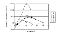
Bi添加量の異なる複数種のBi−PZT強誘電体膜(0.06≦x≦0.21)について各々、分極−電界ヒステリシス測定(PEヒステリシス測定)を行い、残留分極値Pr(μC/cm2)、最大分極値Pmax(μC/cm2)、及び誘電率εを求めた。分極値がほぼ飽和してくるE=100kV/cmにおける分極値をPmaxとして求めた。
<PE hysteresis measurement>
For each of a plurality of types of Bi-PZT ferroelectric films (0.06 ≦ x ≦ 0.21) having different Bi addition amounts, polarization-electric field hysteresis measurement (PE hysteresis measurement) is performed, and remanent polarization value Pr (μC / cm 2 ), the maximum polarization value Pmax (μC / cm 2 ), and the dielectric constant ε. The polarization value at E = 100 kV / cm at which the polarization value is almost saturated was determined as Pmax.
Bi添加量(Aサイト中のモル濃度)と、残留分極値Pr、最大分極値Pmax、及び誘電率εとの関係を図6に示す。図6に示すように、スパッタ法により成膜を行うことにより、焼結助剤やアクセプタイオンを添加することなく、PZTのAサイトに5モル%以上のドナイオンを添加でき、5〜25モル%の範囲内で高い強誘電性能を示すことが明らかとなった。 FIG. 6 shows the relationship between the Bi addition amount (molar concentration in the A site), the remanent polarization value Pr, the maximum polarization value Pmax, and the dielectric constant ε. As shown in FIG. 6, by forming a film by sputtering, 5 mol% or more of donor ions can be added to the A site of PZT without adding a sintering aid or acceptor ions, and 5 to 25 mol%. It was revealed that the ferroelectric performance is high within the range of.
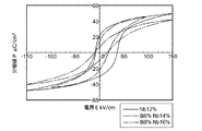
Bi添加量14モル%のBi−PZT強誘電体膜のPEヒステリシス曲線、La添加量1モル%のLa−PZT強誘電体膜のPEヒステリシス曲線、Nb添加量12モル%のNb−PZT強誘電体膜のPEヒステリシス曲線、Bi添加量6モル%−Nb添加量14モル%のBi,Nb−PZT強誘電体膜のPEヒステリシス曲線、及び、Bi添加量9モル%−Nb添加量16モル%のBi,Nb−PZT強誘電体膜のPEヒステリシス曲線を図7A,図7Bに示す。
また、ドナイオンの種類、ドナイオンの添加量、及び(Ec1+Ec2)/(Ec1−Ec2)×100(%)の値の関係を図8に示す。
PE hysteresis curve of Bi-PZT ferroelectric film with 14 mol% Bi added, PE hysteresis curve of La-PZT ferroelectric film with 1 mol% La added, Nb-PZT ferroelectric with 12 mol% Nb added PE hysteresis curve of body film, PE hysteresis curve of Bi, Nb-PZT ferroelectric film with Bi addition amount 6 mol% -
Further, FIG. 8 shows the relationship between the kind of dona ion, the added amount of dona ion, and the value of (Ec1 + Ec2) / (Ec1−Ec2) × 100 (%).
Bサイトに5モル%以上のドナイオンを添加したNb−PZT膜、Ta−PZT膜、及びW−PZT膜では、PEヒステリシスの非対称のレベルを示す(Ec1+Ec2)/(Ec1−Ec2)×100(%)が大きく、25%を超えたのに対し、Aサイトにドナイオンを添加したBi−PZT膜、及びLa−PZT膜では、同パラメータ値が小さく、PEヒステリシスの対称性が良かった。Bi添加量6〜21モル%のBi−PZT膜、及びLa添加量1モル%のLa−PZT膜はいずれも、(Ec1+Ec2)/(Ec1−Ec2)×100(%)≦25であった。 The Nb-PZT film, Ta-PZT film, and W-PZT film with 5 mol% or more of donor ions added to the B site exhibit an asymmetric level of PE hysteresis (Ec1 + Ec2) / (Ec1-Ec2) × 100 (% ) Was large and exceeded 25%, but in the Bi-PZT film and La-PZT film in which donor ions were added to the A site, the parameter value was small and the symmetry of PE hysteresis was good. The Bi-PZT film with a Bi addition amount of 6 to 21 mol% and the La-PZT film with a La addition amount of 1 mol% were both (Ec1 + Ec2) / (Ec1−Ec2) × 100 (%) ≦ 25.
また、Bサイトにのみドナイオンを添加したNb−PZT膜よりも、Aサイト及びBサイトにドナイオンを添加したBi,Nb−PZT膜の方がPEヒステリシスの非対称性は緩和されるが、Bi,Nb共ドープよりもBi単独ドープの方がPEヒステリシスの対称性が格段に良いことが明らかとなった。 In addition, the Bi, Nb-PZT film in which donor ions are added to the A site and the B site is more relaxed than the Nb-PZT film in which donor ions are added only to the B site. It was revealed that the symmetry of PE hysteresis is much better with Bi alone than with co-doping.
(実施例2)
特定の成膜条件を変える以外は実施例1と同様にして、真性PZT膜及びNb−PZT膜の成膜を実施し、それぞれについて強誘電体素子を得た。真性PZT強誘電体膜の成膜ではPb1.3Zr0.52Ti0.48O3ターゲットを用い、Nb−PZT膜の成膜ではPb1.3Zr0.43Ti0.44Nb0.13O3ターゲットを用いて、成膜を行った。
(Example 2)
Intrinsic PZT films and Nb-PZT films were formed in the same manner as in Example 1 except that specific film formation conditions were changed, and ferroelectric elements were obtained for the respective films. A Pb 1.3 Zr 0.52 Ti 0.48 O 3 target is used for forming an intrinsic PZT ferroelectric film, and a Pb 1.3 Zr 0.43 Ti 0.44 Nb 0 is used for forming an Nb-PZT film. The film was formed using a .13 O 3 target.
成膜温度Tsを525℃とし、ターゲットに2.5W/cm2のrf電力を印加し、基板−ターゲット間距離D(mm)=40,60,75,100,120mmの条件で成膜を行った。基板−ターゲット間距離D=60mmではNb−PZT膜を成膜し、それ以外のDにおいてはPZT膜を成膜した。得られた主な膜のXRDパターンを図9〜図13に示す。 Film formation temperature Ts is set to 525 ° C., rf power of 2.5 W / cm 2 is applied to the target, and film formation is performed under conditions of substrate-target distance D (mm) = 40, 60, 75, 100, 120 mm. It was. An Nb-PZT film was formed at a substrate-target distance D = 60 mm, and a PZT film was formed at other distances D. The XRD patterns of the main films obtained are shown in FIGS.
図9〜図13に示すように、成膜温度Ts=525℃の条件では、基板−ターゲット間距離D=40mm〜100mmの範囲内において、結晶配向性を有するペロブスカイト結晶が得られた。図2に対応させると、成膜速度0.5μm/h〜1.2μm/hであり、良好な製造効率でペロブスカイト結晶が得られていることになる。 As shown in FIGS. 9 to 13, perovskite crystals having crystal orientation were obtained in the range of the substrate-target distance D = 40 mm to 100 mm under the condition of the film formation temperature Ts = 525 ° C. Corresponding to FIG. 2, the film formation rate is 0.5 μm / h to 1.2 μm / h, and a perovskite crystal is obtained with good production efficiency.
基板−ターゲット間距離D=120mm(図13参照)では、パイロクロア相がメインの膜が得られたので、「×」と判定した。この場合は、基板―ターゲット間距離Dが長すぎて、成膜速度が遅くなり、ペロブスカイト成長が十分にできなかったと考えられる。基板−ターゲット間距離D=100mm(図12参照)では、同一条件で調製した他のサンプルではパイロクロア相が見られたため、「▲」と判定した。基板−ターゲット間距離D=40mm(図9参照)の場合も、同様にパイロクロア相が見られるため、「▲」と判定した。基板−ターゲット間距離D=60mm及び75mmにおいて、良好な結晶配向性を有するペロブスカイト結晶が安定的に得られたので、「●」と判定した(図10及び図11参照)。 When the substrate-target distance D = 120 mm (see FIG. 13), a film having a pyrochlore phase as the main film was obtained. In this case, it is considered that the substrate-target distance D was too long, the film formation rate was slow, and the perovskite growth could not be sufficiently performed. At the substrate-target distance D = 100 mm (see FIG. 12), a pyrochlore phase was observed in the other samples prepared under the same conditions, and therefore, “▲” was determined. In the case where the substrate-target distance D = 40 mm (see FIG. 9), the pyrochlore phase was similarly seen, and therefore, “▲” was determined. Since perovskite crystals having good crystal orientation were stably obtained at the substrate-target distances D = 60 mm and 75 mm, it was determined as “●” (see FIGS. 10 and 11).
図10に示される圧電膜(D=60mm,Nb−PZT膜)について、XRFによる組成分析を実施した。その結果、図10に示される圧電膜の、Pbのモル量とBサイト元素の合計モル量(Zr+Ti+Nb)との比は、Pb/(Zr+Ti+Nb)=1.02であり、Pb抜けのないNb−PZT膜であることが確認された。 Composition analysis by XRF was performed on the piezoelectric film (D = 60 mm, Nb-PZT film) shown in FIG. As a result, the ratio between the molar amount of Pb and the total molar amount of the B site element (Zr + Ti + Nb) in the piezoelectric film shown in FIG. 10 is Pb / (Zr + Ti + Nb) = 1.02, and Nb− without Pb loss. It was confirmed to be a PZT film.
このNb−PZT膜について、圧電膜上にPt上部電極をスパッタリング法にて100nm厚で形成し、圧電膜の圧電定数d31を片持ち梁法により測定した。基板―ターゲット間距離D=60mmで成膜したものは((100)配向)、圧電定数d31は250pm/Vと高く、良好であった。 This Nb-PZT film, a Pt upper electrode was formed with 100nm thickness by sputtering on the piezoelectric film, and the piezoelectric constant d 31 of the piezoelectric film was measured by a cantilever technique. Films deposited with a substrate-target distance D = 60 mm ((100) orientation) were good, with a high piezoelectric constant d 31 of 250 pm / V.
図12に示される若干のパイロクロア相を含むPZT膜について(D=100mm)、同様に圧電定数d31の測定を行ったところ、d31=110pm/Vであった。 For the PZT film containing a slight pyrochlore phase shown in FIG. 12 (D = 100 mm), the piezoelectric constant d 31 was measured in the same manner, and d 31 = 110 pm / V.
(実施例3)
成膜温度Ts=420℃、基板−ターゲット間距離D=60mmとし、その他の条件は実施例3と同様にしてPZT膜を成膜した。
この条件では、僅かにパイロクロア相を含むものの、(100)配向の、良好な結晶配向性を有するペロブスカイト結晶が得られた。
(Example 3)
A PZT film was formed in the same manner as in Example 3 except that the film formation temperature Ts = 420 ° C. and the substrate-target distance D = 60 mm.
Under this condition, a perovskite crystal having a good crystal orientation with (100) orientation was obtained although it contained a slight pyrochlore phase.
(実施例2,3の結果のまとめ)
図14に、実施例2及び3のすべてのサンプル及びその他の条件で成膜したサンプルについて、成膜温度Tsを横軸にし、基板―ターゲット間距離Dを縦軸にして、XRD測定結果をプロットした
図14には、PZT膜又はNb−PZT膜においては、下記式(1)及び(2)、又は(3)及び(4)を充足する範囲で成膜条件を決定することで、パイロクロア相の少ないペロブスカイト結晶を安定的に成長させることができ、しかもPb抜けを安定的に抑制することができ、結晶構造及び膜組成が良好な良質な圧電膜を安定的に成膜できることが示されている。図14中のデータは真性PZT膜及びNb−PZT膜のデータが混在しているが、真性PZT膜もNb−PZT膜も好適な成膜条件は同様である。
400≦Ts(℃)≦500・・・(1)、
30≦D(mm)≦80・・・(2)、
500≦Ts(℃)≦600・・・(3)、
30≦D(mm)≦100・・・(4)
(Summary of results of Examples 2 and 3)
FIG. 14 plots XRD measurement results for all samples of Examples 2 and 3 and samples formed under other conditions, with the deposition temperature Ts on the horizontal axis and the substrate-target distance D on the vertical axis. In FIG. 14, in the PZT film or the Nb-PZT film, the film formation conditions are determined within a range satisfying the following formulas (1) and (2), or (3) and (4). As a result, it is shown that a perovskite crystal with a small amount of Pb can be stably grown, Pb loss can be stably suppressed, and a high-quality piezoelectric film having a good crystal structure and film composition can be stably formed. Yes. Although the data in FIG. 14 includes data of the intrinsic PZT film and the Nb-PZT film, suitable deposition conditions are the same for the intrinsic PZT film and the Nb-PZT film.
400 ≦ Ts (° C.) ≦ 500 (1),
30 ≦ D (mm) ≦ 80 (2),
500 ≦ Ts (° C.) ≦ 600 (3),
30 ≦ D (mm) ≦ 100 (4)
本発明の強誘電体膜は、インクジェット式記録ヘッド,磁気記録再生ヘッド,MEMS(Micro Electro-Mechanical Systems)デバイス,マイクロポンプ,超音波探触子等に搭載される圧電アクチュエータ、及び強誘電体メモリ等の強誘電体素子に好ましく利用できる。 The ferroelectric film of the present invention includes a piezoelectric actuator mounted on an ink jet recording head, a magnetic recording / reproducing head, a MEMS (Micro Electro-Mechanical Systems) device, a micro pump, an ultrasonic probe, and a ferroelectric memory. It can be preferably used for ferroelectric elements such as.
2 圧電素子(強誘電体素子)
3、3K,3C,3M,3Y インクジェット式記録ヘッド(液体吐出装置)
20 基板
30、50 電極
40 強誘電体膜(圧電体膜)
70 インクノズル(液体貯留吐出部材)
71 インク室(液体貯留室)
72 インク吐出口(液体吐出口)
100 インクジェット式記録装置
2 Piezoelectric elements (ferroelectric elements)
3, 3K, 3C, 3M, 3Y Inkjet recording head (liquid ejection device)
20
70 Ink nozzle (liquid storage and discharge member)
71 Ink chamber (liquid storage chamber)
72 Ink ejection port (liquid ejection port)
100 Inkjet recording device
Claims (19)
(Pb1−x+δMx)(ZryTi1−y)Oz・・・(P)
(式中、MはBi及びランタニド元素からなる群より選ばれた少なくとも1種の元素である。
0.05≦x≦0.4。
0<y≦0.7。
δ=0及びz=3が標準であるが、これらの値はペロブスカイト構造を取り得る範囲内で基準値からずれてもよい。) A perovskite oxide represented by the following formula (P).
(Pb 1-x + δM x ) (Zr y Ti 1-y ) O z (P)
(In the formula, M is at least one element selected from the group consisting of Bi and lanthanide elements.
0.05 ≦ x ≦ 0.4.
0 <y ≦ 0.7.
Although δ = 0 and z = 3 are standard, these values may deviate from the reference value within a range where a perovskite structure can be taken. )
400≦Ts(℃)≦500・・・(1)、
30≦D(mm)≦80・・・(2)
(式(1)及び(2)中、Ts(℃)は成膜温度、D(mm)は基板とターゲットとの離間距離である。) The sputtering method places a target having a composition corresponding to the film composition of the ferroelectric film to be deposited, and the substrate so as to face each other, and on the substrate under film formation conditions satisfying the following expressions (1) and (2): The ferroelectric film according to claim 11, wherein the ferroelectric film is formed.
400 ≦ Ts (° C.) ≦ 500 (1),
30 ≦ D (mm) ≦ 80 (2)
(In formulas (1) and (2), Ts (° C.) is the film forming temperature, and D (mm) is the distance between the substrate and the target.)
500≦Ts(℃)≦600・・・(3)、
30≦D(mm)≦100・・・(4)
(式(3)及び(4)中、Ts(℃)は成膜温度、D(mm)は基板とターゲットとの離間距離である。) The sputtering method places a target having a composition corresponding to the film composition of the ferroelectric film to be deposited, and the substrate so as to face each other under film formation conditions satisfying the following expressions (3) and (4). The ferroelectric film according to claim 11, wherein the ferroelectric film is formed.
500 ≦ Ts (° C.) ≦ 600 (3),
30 ≦ D (mm) ≦ 100 (4)
(In formulas (3) and (4), Ts (° C.) is the film forming temperature, and D (mm) is the distance between the substrate and the target.)
非熱平衡プロセスにより成膜を行うことを特徴とする強誘電体膜の製造方法。 In the manufacturing method of the ferroelectric film in any one of Claims 6-9,
A method for producing a ferroelectric film, wherein the film is formed by a non-thermal equilibrium process.
400≦Ts(℃)≦500・・・(1)、
30≦D(mm)≦80・・・(2)
(式(1)及び(2)中、Ts(℃)は成膜温度、D(mm)は基板とターゲットとの離間距離である。) The sputtering method places a target having a composition corresponding to the film composition of the ferroelectric film to be deposited, and the substrate so as to face each other, and on the substrate under film formation conditions satisfying the following expressions (1) and (2): The method of manufacturing a ferroelectric film according to claim 15, wherein the film is formed.
400 ≦ Ts (° C.) ≦ 500 (1),
30 ≦ D (mm) ≦ 80 (2)
(In formulas (1) and (2), Ts (° C.) is the film forming temperature, and D (mm) is the distance between the substrate and the target.)
500≦Ts(℃)≦600・・・(3)、
30≦D(mm)≦100・・・(4)
(式(3)及び(4)中、Ts(℃)は成膜温度、D(mm)は基板とターゲットとの離間距離である。) The sputtering method places a target having a composition corresponding to the film composition of the ferroelectric film to be deposited, and the substrate so as to face each other under film formation conditions satisfying the following expressions (3) and (4). The method of manufacturing a ferroelectric film according to claim 15, wherein the film is formed.
500 ≦ Ts (° C.) ≦ 600 (3),
30 ≦ D (mm) ≦ 100 (4)
(In formulas (3) and (4), Ts (° C.) is the film forming temperature, and D (mm) is the distance between the substrate and the target.)
液体が貯留される液体貯留室及び該液体貯留室から外部に前記液体が吐出される液体吐出口を有する液体貯留吐出部材とを備えたことを特徴とする液体吐出装置。 A piezoelectric element comprising the ferroelectric element according to claim 18;
A liquid discharge apparatus comprising: a liquid storage chamber in which liquid is stored; and a liquid storage / discharge member having a liquid discharge port through which the liquid is discharged from the liquid storage chamber.
Priority Applications (4)
| Application Number | Priority Date | Filing Date | Title |
|---|---|---|---|
| JP2007229790A JP2009062564A (en) | 2007-09-05 | 2007-09-05 | Perovskite type oxide, ferroelectric film and its manufacturing method, ferroelectric element, and liquid discharge apparatus |
| EP20080015565 EP2034042A3 (en) | 2007-09-05 | 2008-09-03 | Process for forming a ferroelectric film, ferroelectric film, ferroelectric device, and liquid discharge apparatus |
| CN200810214850A CN101665908A (en) | 2007-09-05 | 2008-09-03 | Process for forming a ferroelectric film, ferroelectric film, ferroelectric device, and liquid discharge apparatus |
| US12/204,649 US20090058954A1 (en) | 2007-09-05 | 2008-09-04 | Process for forming a ferroelectric film, ferroelectric film, ferroelectric device, and liquid discharge apparatus |
Applications Claiming Priority (1)
| Application Number | Priority Date | Filing Date | Title |
|---|---|---|---|
| JP2007229790A JP2009062564A (en) | 2007-09-05 | 2007-09-05 | Perovskite type oxide, ferroelectric film and its manufacturing method, ferroelectric element, and liquid discharge apparatus |
Publications (2)
| Publication Number | Publication Date |
|---|---|
| JP2009062564A true JP2009062564A (en) | 2009-03-26 |
| JP2009062564A5 JP2009062564A5 (en) | 2010-04-15 |
Family
ID=40130515
Family Applications (1)
| Application Number | Title | Priority Date | Filing Date |
|---|---|---|---|
| JP2007229790A Withdrawn JP2009062564A (en) | 2007-09-05 | 2007-09-05 | Perovskite type oxide, ferroelectric film and its manufacturing method, ferroelectric element, and liquid discharge apparatus |
Country Status (4)
| Country | Link |
|---|---|
| US (1) | US20090058954A1 (en) |
| EP (1) | EP2034042A3 (en) |
| JP (1) | JP2009062564A (en) |
| CN (1) | CN101665908A (en) |
Families Citing this family (10)
| Publication number | Priority date | Publication date | Assignee | Title |
|---|---|---|---|---|
| JP5410686B2 (en) * | 2008-03-21 | 2014-02-05 | 富士フイルム株式会社 | Piezoelectric film manufacturing method, film forming apparatus, and piezoelectric film |
| JP5854183B2 (en) * | 2010-03-02 | 2016-02-09 | セイコーエプソン株式会社 | Liquid ejecting head, liquid ejecting apparatus, piezoelectric element, ultrasonic sensor and infrared sensor |
| JP5754619B2 (en) * | 2010-03-02 | 2015-07-29 | セイコーエプソン株式会社 | Liquid ejecting head, liquid ejecting apparatus, piezoelectric element, ultrasonic sensor and infrared sensor |
| JP5839157B2 (en) * | 2010-03-02 | 2016-01-06 | セイコーエプソン株式会社 | Liquid ejecting head, liquid ejecting apparatus, piezoelectric element, ultrasonic sensor and infrared sensor |
| JP5854184B2 (en) * | 2010-03-02 | 2016-02-09 | セイコーエプソン株式会社 | Liquid ejecting head, liquid ejecting apparatus, piezoelectric element, ultrasonic sensor and infrared sensor |
| JP5716897B2 (en) * | 2010-03-02 | 2015-05-13 | セイコーエプソン株式会社 | Liquid ejecting head, liquid ejecting apparatus, piezoelectric element, ultrasonic sensor and infrared sensor |
| JP5783256B2 (en) * | 2011-08-26 | 2015-09-24 | 株式会社村田製作所 | Piezoelectric device and method for manufacturing piezoelectric device |
| US9876067B2 (en) * | 2013-03-22 | 2018-01-23 | Japan Science And Technology Agency | Dielectric layer and manufacturing method of dielectric layer, and solid-state electronic device and manufacturing method of solid-state electronic device |
| JP6258241B2 (en) * | 2015-02-27 | 2018-01-10 | 富士フイルム株式会社 | Piezoelectric actuator |
| CN107727845B (en) * | 2017-09-26 | 2019-09-10 | 中国科学院苏州生物医学工程技术研究所 | Lamb wave sensor, biological detection chip and fast screening system |
Family Cites Families (11)
| Publication number | Priority date | Publication date | Assignee | Title |
|---|---|---|---|---|
| JP2532381B2 (en) * | 1986-03-04 | 1996-09-11 | 松下電器産業株式会社 | Ferroelectric thin film element and manufacturing method thereof |
| US6964873B2 (en) * | 1999-10-29 | 2005-11-15 | Fujitsu Limited | Semiconductor device having a ferroelectric capacitor and a fabrication process thereof |
| US6277254B1 (en) * | 1999-12-16 | 2001-08-21 | Honeywell International Inc. | Ceramic compositions, physical vapor deposition targets and methods of forming ceramic compositions |
| JP4266474B2 (en) | 2000-01-21 | 2009-05-20 | キヤノン株式会社 | Method for manufacturing piezoelectric ceramic composition and method for manufacturing piezoelectric element |
| JP4266480B2 (en) | 2000-03-08 | 2009-05-20 | キヤノン株式会社 | Piezoelectric ceramic composition and manufacturing method thereof, piezoelectric element and manufacturing method thereof, and ink jet printer head and ultrasonic motor using the same |
| JP2003301262A (en) * | 2002-04-10 | 2003-10-24 | Sumitomo Metal Mining Co Ltd | Ferroelectric thin film, and sputtering target material for forming ferroelectric thin film |
| JP4324796B2 (en) | 2004-08-30 | 2009-09-02 | セイコーエプソン株式会社 | Ferroelectric film, ferroelectric film manufacturing method, ferroelectric capacitor, and ferroelectric memory |
| JP2006188414A (en) | 2004-12-07 | 2006-07-20 | Murata Mfg Co Ltd | Piezoelectric ceramic composition and piezoelectric ceramic electronic component |
| JP4426488B2 (en) | 2005-03-22 | 2010-03-03 | 三菱樹脂株式会社 | Heat-shrinkable laminated film and molded article and container using the film |
| US20070046153A1 (en) * | 2005-08-23 | 2007-03-01 | Canon Kabushiki Kaisha | Piezoelectric substrate, piezoelectric element, liquid discharge head and liquid discharge apparatus |
| US7998362B2 (en) * | 2005-08-23 | 2011-08-16 | Canon Kabushiki Kaisha | Piezoelectric substance, piezoelectric element, liquid discharge head using piezoelectric element, liquid discharge apparatus, and production method of piezoelectric element |
-
2007
- 2007-09-05 JP JP2007229790A patent/JP2009062564A/en not_active Withdrawn
-
2008
- 2008-09-03 EP EP20080015565 patent/EP2034042A3/en not_active Withdrawn
- 2008-09-03 CN CN200810214850A patent/CN101665908A/en active Pending
- 2008-09-04 US US12/204,649 patent/US20090058954A1/en not_active Abandoned
Also Published As
| Publication number | Publication date |
|---|---|
| CN101665908A (en) | 2010-03-10 |
| US20090058954A1 (en) | 2009-03-05 |
| EP2034042A3 (en) | 2009-11-11 |
| EP2034042A2 (en) | 2009-03-11 |
Similar Documents
| Publication | Publication Date | Title |
|---|---|---|
| JP5367242B2 (en) | Ferroelectric film and manufacturing method thereof, ferroelectric element, and liquid ejection apparatus | |
| JP4505492B2 (en) | Perovskite oxide, ferroelectric film, ferroelectric element, and liquid ejection device | |
| JP5095315B2 (en) | Perovskite oxide, ferroelectric film and manufacturing method thereof, ferroelectric element, and liquid ejection device | |
| JP2009062564A (en) | Perovskite type oxide, ferroelectric film and its manufacturing method, ferroelectric element, and liquid discharge apparatus | |
| US10103316B2 (en) | Piezoelectric film, piezoelectric element including the same, and liquid discharge apparatus | |
| JP2009064859A (en) | Perovskite-type oxide, ferroelectric film and manufacturing method thereof, ferroelectric element, and liquid discharge apparatus | |
| JP2008081801A (en) | Process for forming film, piezoelectric film, piezoelectric device, and liquid discharge apparatus | |
| JP5394765B2 (en) | Perovskite oxide film, ferroelectric, piezoelectric element, liquid ejection device | |
| US10217929B2 (en) | Piezoelectric film, piezoelectric element, and liquid discharge apparatus | |
| JP4246227B2 (en) | Piezoelectric film, method for forming the same, and piezoelectric element | |
| US8210658B2 (en) | Piezoelectric material, method for producing piezoelectric material, piezoelectric device and liquid discharge device | |
| JP4993294B2 (en) | Perovskite oxide, ferroelectric film and manufacturing method thereof, ferroelectric element, and liquid ejection device | |
| JP5290610B2 (en) | Method for forming piezoelectric film | |
| JP2009293130A (en) | Perovskite-type oxide, ferroelectric film, ferroelectric element, and liquid discharge apparatus | |
| JP2007314368A (en) | Perovskite type oxide, ferroelectric element, piezoelectric actuator, and liquid discharge apparatus | |
| JP2009267363A (en) | Perovskite oxide film, ferroelectric, piezoelectric element, and liquid discharging device | |
| US10011111B2 (en) | Piezoelectric film, production method thereof, piezoelectric element, and liquid discharge apparatus | |
| JP4142726B2 (en) | Film-forming method, piezoelectric film, and piezoelectric element | |
| JP4226647B2 (en) | Piezoelectric film, method for forming the same, and piezoelectric element |
Legal Events
| Date | Code | Title | Description |
|---|---|---|---|
| A621 | Written request for application examination |
Free format text: JAPANESE INTERMEDIATE CODE: A621 Effective date: 20100218 |
|
| A521 | Request for written amendment filed |
Free format text: JAPANESE INTERMEDIATE CODE: A523 Effective date: 20100302 |
|
| A761 | Written withdrawal of application |
Free format text: JAPANESE INTERMEDIATE CODE: A761 Effective date: 20110121 |