JP2009059122A - Data processing system - Google Patents
Data processing system Download PDFInfo
- Publication number
- JP2009059122A JP2009059122A JP2007225030A JP2007225030A JP2009059122A JP 2009059122 A JP2009059122 A JP 2009059122A JP 2007225030 A JP2007225030 A JP 2007225030A JP 2007225030 A JP2007225030 A JP 2007225030A JP 2009059122 A JP2009059122 A JP 2009059122A
- Authority
- JP
- Japan
- Prior art keywords
- packet
- integrated circuit
- register
- initiator
- target
- Prior art date
- Legal status (The legal status is an assumption and is not a legal conclusion. Google has not performed a legal analysis and makes no representation as to the accuracy of the status listed.)
- Withdrawn
Links
Images


Classifications
-
- G—PHYSICS
- G06—COMPUTING; CALCULATING OR COUNTING
- G06F—ELECTRIC DIGITAL DATA PROCESSING
- G06F13/00—Interconnection of, or transfer of information or other signals between, memories, input/output devices or central processing units
- G06F13/38—Information transfer, e.g. on bus
- G06F13/40—Bus structure
- G06F13/4004—Coupling between buses
- G06F13/4027—Coupling between buses using bus bridges
- G06F13/4045—Coupling between buses using bus bridges where the bus bridge performs an extender function
-
- Y—GENERAL TAGGING OF NEW TECHNOLOGICAL DEVELOPMENTS; GENERAL TAGGING OF CROSS-SECTIONAL TECHNOLOGIES SPANNING OVER SEVERAL SECTIONS OF THE IPC; TECHNICAL SUBJECTS COVERED BY FORMER USPC CROSS-REFERENCE ART COLLECTIONS [XRACs] AND DIGESTS
- Y02—TECHNOLOGIES OR APPLICATIONS FOR MITIGATION OR ADAPTATION AGAINST CLIMATE CHANGE
- Y02D—CLIMATE CHANGE MITIGATION TECHNOLOGIES IN INFORMATION AND COMMUNICATION TECHNOLOGIES [ICT], I.E. INFORMATION AND COMMUNICATION TECHNOLOGIES AIMING AT THE REDUCTION OF THEIR OWN ENERGY USE
- Y02D10/00—Energy efficient computing, e.g. low power processors, power management or thermal management
Landscapes
- Engineering & Computer Science (AREA)
- General Engineering & Computer Science (AREA)
- Theoretical Computer Science (AREA)
- Computer Hardware Design (AREA)
- Physics & Mathematics (AREA)
- General Physics & Mathematics (AREA)
- Information Transfer Systems (AREA)
- Communication Control (AREA)
- Data Exchanges In Wide-Area Networks (AREA)
Abstract
Description
本発明は、複数個の半導体集積回路をスプリットトランザクションインタフェースで接続したデータ処理システムにおけるスプリットトランザクションインタフェース制御に関する。 The present invention relates to split transaction interface control in a data processing system in which a plurality of semiconductor integrated circuits are connected by a split transaction interface.
システム・オン。チップ(SoC)に対する要求性能や要求機能は年々上がっており、この傾向は今後も継続する見込みである。これに伴い、SoCに集積される回路量が増加し、増加する回路を搭載するためにさらに微細化技術が高度化するが、これらは相乗効果によって、マスクコストなど、SoCの開発費を急騰させる。したがって、SoCベンダが収益を上げるために必要な量産数量、つまり採算ラインが、近年急上昇しつつあり、この傾向は継続する見込みである。現在でもSoCを全面的に先端プロセスを用いて開発していては採算ラインに達しない案件があるが、今後はこのような案件の比率がより高まると予想される。 System on. The required performance and required functions for chips (SoC) are increasing year by year, and this trend is expected to continue. Along with this, the amount of circuits integrated in the SoC will increase, and further miniaturization technology will become more sophisticated in order to mount increasing circuits, but these will rapidly increase SoC development costs such as mask costs due to synergistic effects. . Therefore, the mass production volume necessary for SoC vendors to increase their profits, that is, the profit line, has been rising rapidly in recent years, and this trend is expected to continue. Even now, there are cases where SoC is fully developed using advanced processes and does not reach the profit line, but in the future, the ratio of such cases is expected to increase further.
そこで今後は、先端プロセス製品の採算性確保と、個別顧客対応を同時に実現するために、複数品種に共通する機能を先端プロセスでASSPとして開発し、顧客対応部分をASICとして安価なプロセスで開発する、ASSP・ASIC分離アーキテクチャが広まる見込みである。ASSP(Application Specific Standard Product)とは特定の分野を対象に機能を特化させた汎用LSIを意味する。ASIC(Application Specific Integrated Circuit)とはある特定の用途のために設計、製造される専用LSAIを意味し、カスタムチップなどとも呼ばれる。 Therefore, in the future, in order to ensure profitability of advanced process products and support individual customers at the same time, functions common to multiple products will be developed as advanced processes using ASSP, and customer-facing parts will be developed as inexpensive processes using ASICs. ASSP / ASIC separation architecture is expected to spread. ASSP (Application Specific Standard Product) means a general-purpose LSI that specializes functions for a specific field. ASIC (Application Specific Integrated Circuit) means a dedicated LSAI designed and manufactured for a specific application, and is also called a custom chip.
ASSP・ASIC分離アーキテクチャでは、チップ間転送の重要度が高い。特に、メインCPUを搭載するASSPから周辺機能を搭載するASICへのアクセス性能が重要である。従来、チップ間インタフェースとしては、PCI(Peripheral Components Interconnect)等の数十メガヘルツ程度で動作するパラレルバスが多く用いられていたが、パラレルバスには、端子数が多いためにチップコストが上がりやすく、必要な配線が多いためにチップを搭載する基板のコストが上がりやすい課題がある。 In the ASSP / ASIC separation architecture, the importance of transfer between chips is high. In particular, the access performance from the ASSP in which the main CPU is mounted to the ASIC in which peripheral functions are mounted is important. Conventionally, as a chip-to-chip interface, a parallel bus that operates at about several tens of megahertz such as PCI (Peripheral Components Interconnect) has been used in many cases. There is a problem that the cost of the substrate on which the chip is mounted tends to increase due to the large number of necessary wirings.
そこで、数百メガヘルツ以上に動作周波数を高めて端子数を削減したシリアルインタフェースが、チップ間インタフェースとして必要となる。このような周波数で動作するチップ間インタフェースでは、数十メガヘルツで動作するパラレルインタフェースが採用している、ハンドシェイク信号によるフロー制御の実装は困難である。 Therefore, a serial interface in which the operating frequency is increased to several hundred megahertz or more to reduce the number of terminals is required as an inter-chip interface. In an inter-chip interface operating at such a frequency, it is difficult to implement flow control using a handshake signal, which is adopted by a parallel interface operating at several tens of megahertz.
特許文献1には、バスの高速周波数での動作を可能にするために、発行側LSIは、受信側LSIが何個のコマンドを同時に処理できるか、或いは何個のデータを同時に受信できるかを示す値が初期化時にロードされるカウンタを有し、コマンドまたはデータを発行する時に、カウンタをデクリメントし、レディ信号を受信したときにカウンタをインクリメントし、カウンタが0になればコマンドまたはデータの発行を抑止するというインタフェースプロトコルを開示する。これによれば、発行側LSIは、受信側LSIからのビジー信号を確認することなく、受信側LSIに対してコマンドやデータの発行をすることができる。コマンドまたはデータの発行側LSIが、受信側LSIのコマンドバッファまたはデータバッファの状態を管理できるので、バスが高速で動作するようになっても、ハンドシェークによらずに、効率よくコマンドまたはデータを発行することができる。
In
特許文献2に記載の技術において、送信手段11は、応答手段21からの応答確認をとらずに情報フレームを連続送信し、計数手段12からの最大アウトスタンディング数と送信された情報フレームの数との一致結果に基づき次に送信する情報フレームのポールビットを「1」にして送信する。送信手段11は、応答手段からのファイナルビットが「1」のレスポンスフレームを受信し、再び情報フレームをそのポールビットを「0」にしてデータ受信装置の応答確認をとらずに連続送信する。これにより、応答未確認での情報フレームの連続送信ができ、かつ応答確認がすぐに返信されデータ効率を向上できる、とある。
In the technique described in
上記特許文献に記載の技術によれば、ハンドシェイク信号線に依らずにフロー制御を実現することができるため、イニシエータ回路とターゲット回路の間の信号の動作を高速化することができる。これにより、シリアルインタフェースには、従来のハンドシェイク信号によるフロー制御に代えて、アウトスタンディング・ベースのフロー制御が有用であることが理解される。本発明者は更に進んで、リクエストを発行してからレスポンスを受取るまでのレイテンシの抑制と低消費電力に寄与することができるアウトスタンディング・ベースのフロー制御について検討した。更に本発明者は、それに関連してフロー制御の可変性、可変フロー制御に起因して割込み処理が遅延する可能性の回避、インタフェース信号の秘匿性の向上などについて検討し、本発明を完成した。 According to the technique described in the above-mentioned patent document, since flow control can be realized without depending on the handshake signal line, the signal operation between the initiator circuit and the target circuit can be speeded up. Accordingly, it is understood that the standing-based flow control is useful for the serial interface instead of the flow control by the conventional handshake signal. The present inventor has further studied an outstanding-based flow control that can contribute to the suppression of latency and the low power consumption from when a request is issued until a response is received. Further, the inventor studied the variability of flow control, avoiding the possibility of delay of interrupt processing due to variable flow control, and improving the confidentiality of interface signals, and completed the present invention. .
本発明の目的は、レイテンシの抑制と低消費電力に寄与することができるアウトスタンディング・ベースのフロー制御を実現することにある。 An object of the present invention is to realize standing-based flow control that can contribute to latency suppression and low power consumption.
本発明の別の目的は、アウトスタンディング・ベースの可変フロー制御を可能にするデータ処理システムを実現することにある。 Another object of the present invention is to provide a data processing system that enables outstanding-based variable flow control.
本発明の更に別の目的は、チップ間での割り込み情報の通信に関し、可変フロー制御に起因して割込み処理が遅延す可能性を回避することにある。 Still another object of the present invention relates to communication of interrupt information between chips, and is to avoid the possibility of delaying interrupt processing due to variable flow control.
本発明の前記並びにその他の目的と新規な特徴は本明細書の記述及び添付図面から明らかになるであろう。 The above and other objects and novel features of the present invention will be apparent from the description of this specification and the accompanying drawings.
本願において開示される発明のうち代表的なものの概要を簡単に説明すれば下記の通りである。 The following is a brief description of an outline of typical inventions disclosed in the present application.
〔1〕データ処理システムは、イニシエータを有する第1の半導体集積回路と、ターゲットを有する第2の半導体集積回路と、前記イニシエータと前記ターゲットとを接続するインタフェース信号線とを有し、前記イニシエータがリクエストパケットを前記ターゲットに送信し、前記ターゲットがレスポンスパケットを前記イニシエータに送信することにより、パケットベースのスプリットトランザクションインタフェースを行う。このデータ処理システムにおいて、前記イニシエータは送信したリクエストパケットの数と受信したレスポンスパケットの数の差分値であるアウトスタンディング数を計数するアウトスタンディング計数回路を備え、前記アウトスタンディング数計数回路の計数値が、ターゲットが対応可能なアウトスタンディング数以下となるようにリクエストパケット送信数を制御する。この制御により、リクエストパケットを発行してからレスポンスパケットを受け取るまでの最大レイテンシを抑制するように、アウトスタンディング数を適切な数に動的に変更することが可能になる。 [1] A data processing system includes a first semiconductor integrated circuit having an initiator, a second semiconductor integrated circuit having a target, and an interface signal line connecting the initiator and the target. A request packet is transmitted to the target, and the target transmits a response packet to the initiator, thereby performing a packet-based split transaction interface. In this data processing system, the initiator includes an outstanding counting circuit that counts an outstanding number that is a difference value between the number of transmitted request packets and the number of received response packets, and the count value of the outstanding number counting circuit is The number of request packets transmitted is controlled so that the target is equal to or less than the number of standings that can be handled. This control makes it possible to dynamically change the number of standings to an appropriate number so as to suppress the maximum latency from issuing a request packet to receiving a response packet.
〔2〕項1において前記ターゲットが、対応可能なアウトスタンディング数を保持するアウトスタンディングレジスタを備えるとき、前記イニシエータは、前記アウトスタンディングレジスタの値を読み出し、前記読み出した値が前記アウトスタンディング計数回路の計数値以下となるようにリクエストパケット送信数を制御する。これにより、前記アウトスタンディングレジスタに設定された値にしたがって前記リクエストパケット送信数を制御することができる。
[2] When the target includes an standing register that holds a corresponding number of outstandings in
〔3〕項1において前記ターゲットが、対応可能なアウトスタンディング数を保持するアウトスタンディングレジスタを備えるとき、前記イニシエータは、前記アウトスタンディングレジスタにアウトスタンディング数を設定し、前記設定した値が前記アウトスタンディング計数回路の計数値以下となるようにリクエストパケット送信数を制御する。これにより、イニシエータは、前記アウトスタンディングレジスタに所要の値を設定して前記リクエストパケット送信数を制御することができる。
[3] In the
〔4〕項1において前記イニシエータは、リクエストパケットと同じ転送経路を用いて割り込みパケットを前記ターゲットに送信し、前記ターゲットは、受信した割り込みパケットに基づいて割り込み信号を生成する。これにより、イニシエータ側からターゲット側に発行した割り込み要求に対する割り込み応答性のレイテンシについても可変に制御することが可能になる。
[4] In
〔5〕項1において前記ターゲットは、レスポンスパケットと同じパケット転送経路を用いて割り込みパケットを前記イニシエータに送信し、前記イニシエータは受信した割り込みパケットに基づいて割り込み信号を生成する。これにより、ターゲット側からイニシエータ側に発行した割り込み要求に対する割り込み応答性のレイテンシについても可変に制御することが可能になる。
[5] In
〔6〕項2又は3において前記ターゲットは、前記アウトスタンディングレジスタに保持された最大アウトスタンディング数に対応する数のパケットのデータを保持することが可能な複数のバッファを有し、前記アウトスタンディングレジスタに保持されたアウトスタンディング数に対応する数のパケットのデータを保持する必要のないバッファへの電力供給を遮断する。これにより、リクエストパケットに応答するターゲットの低消費電力に寄与することができる。
[6] In the
〔7〕項2又は3において、前記ターゲットは、前記アウトスタンディングレジスタに保持された最大アウトスタンディング数に対応する数のパケットのデータを保持することが可能な複数のバッファを有し、前記アウトスタンディングレジスタに保持されたアウトスタンディング数に対応する数のパケットのデータを保持する必要のないバッファへのクロック供給を遮断する。これにより、リクエストパケットに応答するターゲットの低消費電力に寄与することができる。
[7] In
〔8〕項1において、前記イニシエータはターゲットに、リクエストパケットを復号するための第1の暗号鍵とレスポンスパケットを暗号化するための第2の暗号鍵を供給し、前記ターゲットは、受信したリクエストパケットを前記第1の暗号鍵を用いて復号し、送信するレスポンスパケットを前記第2の暗号鍵を用いて暗号化する。これによりイニシエータとターゲットと野間のインタフェース信号の秘匿性を向上させることができる。
[8] In
〔9〕データ処理システムは、イニシエータを有する第1の半導体集積回路と、ターゲットを有する第2の半導体集積回路と、前記イニシエータと前記ターゲットとを接続するインタフェース信号線とを有し、前記イニシエータがリクエストパケットを前記ターゲットに送信し、前記ターゲットがレスポンスパケットを前記イニシエータに送信することにより、パケットベースのスプリットトランザクションインタフェースを行う。前記イニシエータは、送信したリードアクセスのリクエストパケットの数と受信したリードアクセスのレスポンスパケットの数の差分値であるリードアウトスタンディング数を計数するリードアウトスタンディング計数回路を備え、前記リードアウトスタンディング数計数回路の計数値が、ターゲットが対応可能なリードアウトスタンディング数以下となるように、リードアクセスのリクエストパケット送信数を制御する。この制御により、リードアクセスのリクエストパケットを発行してからレスポンスパケットを受け取るまでの最大レイテンシを抑制するように、アウトスタンディング数を適切な数に動的に変更することが可能になる。 [9] A data processing system includes a first semiconductor integrated circuit having an initiator, a second semiconductor integrated circuit having a target, and an interface signal line connecting the initiator and the target. A request packet is transmitted to the target, and the target transmits a response packet to the initiator, thereby performing a packet-based split transaction interface. The initiator includes a lead-out standing count circuit that counts a lead-out standing number that is a difference value between the number of read access request packets and the number of received read access response packets. The number of read access request packets transmitted is controlled so that the count value of the number is less than or equal to the number of lead-out standings that can be handled by the target. With this control, the number of outstandings can be dynamically changed to an appropriate number so as to suppress the maximum latency from when a read access request packet is issued until a response packet is received.
〔10〕データ処理システムは、イニシエータを有する第1の半導体集積回路と、ターゲットを有する第2の半導体集積回路と、前記イニシエータと前記ターゲットとを接続するインタフェース信号線とを有し、前記イニシエータがリクエストパケットを前記ターゲットに送信し、前記ターゲットがレスポンスパケットを前記イニシエータに送信することにより、パケットベースのスプリットトランザクションインタフェースを行う。前記イニシエータは、送信したライトアクセスのリクエストパケットの数と受信したライトアクセスのレスポンスパケットの数の差分値であるライトアウトスタンディング数を計数するライトアウトスタンディング計数回路を備え、前記ライトアウトスタンディング数計数回路の計数値が、ターゲットが対応可能なライトアウトスタンディング数以下となるように、ライトアクセスのリクエストパケット送信数を制御する。この制御により、ライトアクセスのリクエストパケットを発行してからレスポンスパケットを受け取るまでの最大レイテンシを抑制するように、アウトスタンディング数を適切な数に動的に変更することが可能になる。 [10] A data processing system includes a first semiconductor integrated circuit having an initiator, a second semiconductor integrated circuit having a target, and an interface signal line connecting the initiator and the target. A request packet is transmitted to the target, and the target transmits a response packet to the initiator, thereby performing a packet-based split transaction interface. The initiator includes a write-out standing count circuit that counts a write-out standing count that is a difference value between the number of transmitted write access request packets and the number of received write access response packets. The number of request packets transmitted for write access is controlled so that the count value is equal to or less than the number of write-out standings that can be handled by the target. With this control, the number of outstandings can be dynamically changed to an appropriate number so as to suppress the maximum latency from when a write access request packet is issued until a response packet is received.
〔11〕データ処理システムは、イニシエータを有する第1の半導体集積回路と、ターゲットを有する第2の半導体集積回路と、前記イニシエータと前記ターゲットとを接続するインタフェース信号線とを有し、前記イニシエータがリクエストパケットを前記ターゲットに送信し、前記ターゲットがレスポンスパケットを前記イニシエータに送信することにより、パケットベースのスプリットトランザクションインタフェースを行う。前記イニシエータは、リクエストパケットの転送タイミングを示すリクエストストローブ信号とリクエストパケットをターゲットに送信する。前記ターゲットは、レスポンスパケットの転送タイミングを示すレスポンスストローブ信号とレスポンスパケットをイニシエータに送信する。これにより、ストローブ信号を用いてフロー制御のタイミングを可変制御することができる。 [11] A data processing system includes a first semiconductor integrated circuit having an initiator, a second semiconductor integrated circuit having a target, and an interface signal line connecting the initiator and the target. A request packet is transmitted to the target, and the target transmits a response packet to the initiator, thereby performing a packet-based split transaction interface. The initiator transmits a request strobe signal indicating a request packet transfer timing and a request packet to the target. The target transmits a response strobe signal indicating the transfer timing of the response packet and a response packet to the initiator. As a result, the flow control timing can be variably controlled using the strobe signal.
〔12〕データ処理システムは、イニシエータを有する第1の半導体集積回路と、ターゲットを有する第2の半導体集積回路と、前記イニシエータと前記ターゲットとを接続するインタフェース信号線とを有し、前記イニシエータがリクエストパケットを前記ターゲットに送信し、前記ターゲットがレスポンスパケットを前記イニシエータに送信することにより、パケットベースのスプリットトランザクションインタフェースを行う。前記ターゲットは、リクエストパケットの受信に用いる信号線の本数を保持するリクエストレーン数レジスタとレスポンスパケットの送信に用いる信号線の本数を保持するレスポンスレーン数レジスタを備える。前記イニシエータは、前記リクエストレーン数レジスタにリクエストパケットの送信に用いる信号線の本数を示す値を、前記レスポンスレーン数レジスタにレスポンスリクエストパケットの受信に用いる信号線の本数を示す値をそれぞれ設定する。これにより、レーン数レジスタの設定値にしたがってフロー制御に用いる信号線本数を可変制御することができる。 [12] A data processing system includes a first semiconductor integrated circuit having an initiator, a second semiconductor integrated circuit having a target, and an interface signal line connecting the initiator and the target. A request packet is transmitted to the target, and the target transmits a response packet to the initiator, thereby performing a packet-based split transaction interface. The target includes a request lane number register for holding the number of signal lines used for receiving a request packet and a response lane number register for holding the number of signal lines used for transmitting a response packet. The initiator sets a value indicating the number of signal lines used for transmitting the request packet in the request lane number register, and sets a value indicating the number of signal lines used for receiving the response request packet in the response lane number register. Thereby, the number of signal lines used for flow control can be variably controlled according to the set value of the lane number register.
〔13〕項12において、前記イニシエータは、リクエストパケットのビット数を計数するリクエスト計数回路とレスポンスパケットのビット数を計数するレスポンス計数回路を備え、前記リクエスト計数回路の計数結果と前記レスポンス計数回路の計数結果に基づいてリクエストパケットの受信に用いる信号線の本数とレスポンスパケットの受信に用いる信号線の本数を設定する。
[13] In
〔14〕データ処理システムは、スプリットトランザクションインタフェースにより通信を行うイニシエータとターゲットを夫々が有する第1半導体集積回路及び第2半導体集積回路を備える。前記第1半導体集積回路と前記第2半導体集積回路が通信用の信号線で接続される。前記第1半導体集積回路は、前記第2半導体集積回路のイニシエータを停止させた後に前記信号線の本数を変更する。これにより、第1半導体集積回路のターゲットがリクエストパケットを正常に受信できなくなる事態を抑制して、信号線本数を可変にできる。 [14] The data processing system includes a first semiconductor integrated circuit and a second semiconductor integrated circuit each having an initiator and a target that perform communication using a split transaction interface. The first semiconductor integrated circuit and the second semiconductor integrated circuit are connected by a communication signal line. The first semiconductor integrated circuit changes the number of the signal lines after stopping the initiator of the second semiconductor integrated circuit. As a result, the situation where the target of the first semiconductor integrated circuit cannot normally receive the request packet can be suppressed, and the number of signal lines can be made variable.
〔15〕データ処理システムは、スプリットトランザクションインタフェースにより暗号化情報の通信を行うイニシエータとターゲットを夫々が有する第1半導体集積回路及び第2半導体集積回路を備える。前記第1半導体集積回路と前記第2半導体集積回路が通信用の信号線で接続される。前記第1半導体集積回路は、前記第2半導体集積回路のイニシエータを停止させた後に暗号化に使用される暗号鍵を変更する。これにより、第1半導体集積回路のターゲットがリクエストパケットを正常に復号できなくなる事態を抑制して、暗号鍵を可変にできる。 [15] The data processing system includes a first semiconductor integrated circuit and a second semiconductor integrated circuit each having an initiator and a target that communicate encrypted information through a split transaction interface. The first semiconductor integrated circuit and the second semiconductor integrated circuit are connected by a communication signal line. The first semiconductor integrated circuit changes the encryption key used for encryption after stopping the initiator of the second semiconductor integrated circuit. As a result, it is possible to change the encryption key by suppressing the situation where the target of the first semiconductor integrated circuit cannot normally decrypt the request packet.
〔16〕データ処理システムは、スプリットトランザクションインタフェースにより通信を行うイニシエータとターゲットを夫々が有する第1半導体集積回路及び第2半導体集積回路を備える。前記第1半導体集積回路と前記第2半導体集積回路が通信用の信号線で接続される。前記第1半導体集積回路は、前記第1半導体集積回路が備えるターゲットのアウトスタンディング数上限値に基づいて前記第2半導体集積回路のイニシエータのアウトスタンディング上限数を設定する。これにより、第1半導体集積回路のターゲットが第2半導体集積回路のイニシエータからのリクエストパケットに正常に応答できなくなる事態を抑制して、アウトスタンディング数を可変にできる。 [16] The data processing system includes a first semiconductor integrated circuit and a second semiconductor integrated circuit each having an initiator and a target that perform communication using a split transaction interface. The first semiconductor integrated circuit and the second semiconductor integrated circuit are connected by a communication signal line. The first semiconductor integrated circuit sets an upper limit number of standing of the initiator of the second semiconductor integrated circuit based on an upper limit value of the number of outstanding targets of the target included in the first semiconductor integrated circuit. As a result, a situation in which the target of the first semiconductor integrated circuit cannot normally respond to the request packet from the initiator of the second semiconductor integrated circuit is suppressed, and the number of standings can be made variable.
本願において開示される発明のうち代表的なものによって得られる効果を簡単に説明すれば下記のとおりである。 The effects obtained by the representative ones of the inventions disclosed in the present application will be briefly described as follows.
レイテンシの抑制と低消費電力に寄与することができるアウトスタンディング・ベースのフロー制御を実現することができる。 It is possible to realize standing-based flow control that can contribute to latency suppression and low power consumption.
アウトスタンディング・ベースの可変フロー制御を可能にするデータ処理システムを実現することができる。 A data processing system can be implemented that enables outstanding-based variable flow control.
チップ間での割り込み情報の通信に関し、可変フロー制御に起因して割込み処理が遅延す可能性を回避することができる。 Regarding communication of interrupt information between chips, it is possible to avoid the possibility of delay of interrupt processing due to variable flow control.
《第1の実施の形態》
図1には本発明の一例にかかる集積回路Aおよび集積回路Bが示される。同図に示される集積回路A101および集積回路B109は、公知のCMOS(相補型MOSトランジスタ)やバイポーラトランジスタなどを形成する半導体集積回路技術によって、単結晶シリコンのような半導体基板に形成される。本実施の形態では、本発明による集積回路A101と集積回路B109の間のリードアクセス、ライトアクセスおよび集積回路B109から集積回路A101への割り込み通知について説明する。
<< First Embodiment >>
FIG. 1 shows an integrated circuit A and an integrated circuit B according to an example of the present invention. The integrated circuit A101 and the integrated circuit B109 shown in the figure are formed on a semiconductor substrate such as single crystal silicon by a semiconductor integrated circuit technique for forming a known CMOS (complementary MOS transistor), bipolar transistor, or the like. In this embodiment, read access and write access between the integrated circuit A101 and the integrated circuit B109 and notification of an interrupt from the integrated circuit B109 to the integrated circuit A101 according to the present invention will be described.
まず、信号線群AB107と信号線群BA108について図面を参照して説明する。 First, the signal line group AB107 and the signal line group BA108 will be described with reference to the drawings.
図2は、信号線群AB107と信号線群BA108を示す図である。3ステートバッファ201および202は、信号伝送方向を切り替えるための3ステートバッファである。プルアップ抵抗203は、信号線群AB107あるいは信号線群BA108に含まれる情報信号線群が集積回路A101にも集積回路B109にも駆動されていないときに、該情報信号線群の電位をHIGHレベルに固定するためのプルアップ抵抗である。
FIG. 2 is a diagram illustrating the signal line group AB107 and the signal line group BA108. The 3-
信号線群AB107は、集積回路A101から集積回路B109に情報を伝送する信号線群であり、信号線群BA108は、集積回路B109から集積回路A101に情報を伝送する信号線群である。信号線群AB107および信号線群BA108は、SiP(System in Package)内のボンディングワイヤやバンプやインタポーザ、基板上の配線等によって形成される。 The signal line group AB107 is a signal line group that transmits information from the integrated circuit A101 to the integrated circuit B109, and the signal line group BA108 is a signal line group that transmits information from the integrated circuit B109 to the integrated circuit A101. The signal line group AB107 and the signal line group BA108 are formed by bonding wires, bumps, interposers, wirings on a substrate, etc. in a SiP (System in Package).
信号線群AB107は、1本のストローブ信号1201と2本の情報信号群AB1202と2本の情報信号群1205を含む。信号線群AB107は、集積回路A101のイニシエータA105に含まれる暗号化送信部A1104によって駆動される。以下、本実施の形態では、情報信号群AB1202および情報信号群1205をリクエストレーンといい、情報信号群AB1202および情報信号群1205の信号線のうち、シリアルパケットの伝送に使用される信号線の本数をリクエストレーン数という。
The signal line group AB107 includes one
信号線群BA108は、1本のストローブ信号1203と2本の情報信号群AB1204と2本の情報信号群BA1205を含む。信号線群BA108は、集積回路B109のターゲットB112に含まれる暗号化送信部B1302によって駆動される。以下、本実施の形態では、情報信号群BA1204および情報信号群BA1205をレスポンスレーンといい、情報信号群BA1204および情報信号群BA1205のうち、伝送に使用される信号線の本数をレスポンスレーン数という。
The signal line group BA108 includes one
ただし、情報信号群AB1205は、転送方向を切り替えられるように3ステートバッファ201および202によって駆動される。該情報信号群BA1205は、伝送方向が集積回路BA109から集積回路AB101の方向であるときにはリクエストレーンに属して信号線群AB107に含まれ、伝送方向が集積回路AB101から集積回路BA109の方向であるときにはレスポンスレーンに属して信号線群BA108に含まれる。
However, the information
つづいて、集積回路A101に含まれるモジュールについて、再び図1を参照して説明する。 Next, modules included in the integrated circuit A101 will be described with reference to FIG. 1 again.
集積回路A101は、CPUA102と、メモリA103と、INTCA104と、イニシエータA105と、ルータA106の各モジュールを備えて構成される。また、集積回路A101には、信号線群AB107と信号線群BA108が接続される。CPUA102は、ルータA106を介してメモリA103にアクセスし、該メモリに保持されているプログラムを実行することによって、集積回路A101および集積回路B109の制御を行うプロセッサである。
The integrated circuit A101 includes modules of a CPU A102, a memory A103, an
ここで、本発明によるアクセスに用いられるスプリットトランザクションインタフェースプロトコル(スプリットプロトコル)を説明する。 Here, the split transaction interface protocol (split protocol) used for access according to the present invention will be described.
集積回路A101内のアクセスは、アクセスを要求するモジュールがアクセス要求を送信し、アクセス要求を受信したモジュールが、アクセスを要求したモジュールに対してアクセス応答を送信することによって完結するスプリットプロトコルにて行われる。 Access in the integrated circuit A101 is performed by a split protocol that is completed by a module requesting access transmitting an access request and the module receiving the access request transmitting an access response to the module requesting access. Is called.
本明細書においては、アクセスを要求するモジュールをイニシエータといい、アクセスに応答する回路若しくはモジュールをターゲットという。一つの回路でイニシエータとターゲットの機能を持つ場合もある。また、本明細書においては、アクセス要求の数とアクセス応答の数の差分をアウトスタンディング数という。アウトスタンディング数が1であれば、イニシエータが送信したアクセス要求に対してターゲットがアクセス応答を返信するまで、イニシエータは別のアクセス要求を送信しない。アウトスタンディングが2以上であれば、イニシエータは、送信したアクセス要求に対するアクセス応答を受信する前に別のアクセス要求を送信することができ、ターゲットは受信したアクセス要求に対してアクセス応答を返信する前に、別のアクセス要求を受信することができる。 In this specification, a module that requests access is called an initiator, and a circuit or module that responds to access is called a target. In some cases, one circuit has the functions of an initiator and a target. Further, in this specification, the difference between the number of access requests and the number of access responses is referred to as an outstanding number. If the outstanding number is 1, the initiator does not transmit another access request until the target returns an access response to the access request transmitted by the initiator. If the outstanding is 2 or more, the initiator can transmit another access request before receiving an access response to the transmitted access request, and the target can return an access response to the received access request. In addition, another access request can be received.
アウトスタンディング数の上限値が大きければ、単位時間内に多くのアクセス要求やアクセス応答を処理できるため、転送スループットを高め易い。しかしながら、大きなアウトスタンディング数は、多くのアクセスを同時に処理するために多くの回路が必要であることを意味し、回路コストが増大することを意味する。 If the upper limit of the number of outstandings is large, many access requests and access responses can be processed within a unit time, so that it is easy to increase transfer throughput. However, a large outstanding number means that many circuits are required to process many accesses at the same time, which means that the circuit cost increases.
つづいて、集積回路A101内におけるアクセスを、図面を参照して説明する。 Next, access in the integrated circuit A101 will be described with reference to the drawings.
図3は、集積回路A101内部において、ライトアクセスとリードアクセスをそれぞれ1回行う場合を示すタイミングチャートである。図3の時刻T1からT5までがライトアクセスである。ライトアクセスでは、イニシエータがアクセス要求の内容であるアドレス“A1”、コマンド“C1”、ライトデータ“D1”、リクエストID“R1”を出力し、アクセス要求が送信されていることを示すリクエストバリッド信号をハイ(HIGH)レベルに遷移させる(時刻T1)。リクエストIDは、ターゲットがアクセス応答をイニシエータに送信するときに、該アクセス応答を中継するルータA106が送信先のイニシエータを特定できるように、イニシエータがアクセス要求に含める識別情報である。
FIG. 3 is a timing chart showing a case where the write access and the read access are each performed once in the integrated circuit A101. Write access is from time T1 to T5 in FIG. In write access, the initiator outputs the address “A1”, the command “C1”, the write data “D1”, and the request ID “R1”, which are the contents of the access request, and a request valid signal indicating that the access request is transmitted Is shifted to a high level (time T1). The request ID is identification information that the initiator includes in the access request so that when the target transmits an access response to the initiator, the
ルータA106は、アドレスによって送信先のターゲットを特定し、該特定されたターゲットにイニシエータが送信したアドレス、コマンド、ライトデータ、リクエストIDを再送信する。このとき、該ターゲットに対してリクエストバリッド信号をアサートしてアクセス要求が送信されていることを通知する。
The
以下、本明細書では、前記リクエストバリッド信号などの1ビットの制御信号を出力するモジュールが、前記制御信号を有意な状態であることを示す値に遷移させることを「アサートする」と表現し、有意ではない状態であることを示す値に遷移させることを「ディアサートする」と表現する。また、1ビットの制御信号が有意な状態であることを示す値であることを「アサート状態」と表現し、1ビットの制御信号が有意な状態でないことを示す値であることを「ディアサート状態」と表現する。さらに、本明細書では、アドレス、コマンド、ライトデータ、リクエストIDなど、アクセス要求内容を示す情報をリクエストパケットといい、ステータス、リードデータ、レスポンスバリッドなど、アクセス応答内容を示す情報をレスポンスパケットという。 Hereinafter, in the present specification, a module that outputs a 1-bit control signal such as the request valid signal transitions the control signal to a value indicating a significant state is expressed as “assert”. Transitioning to a value indicating a non-significant state is expressed as “deasserting”. Further, a value indicating that the 1-bit control signal is in a significant state is expressed as “asserted state”, and a value indicating that the 1-bit control signal is not in a significant state is expressed as “deasserted”. "State". Further, in this specification, information indicating access request contents such as address, command, write data, and request ID is referred to as a request packet, and information indicating access response contents such as status, read data, and response valid is referred to as a response packet.
さらに、集積回路A101を転送されるリクエストパケット、レスポンスパケットを、後述の集積回路A101と集積回路B109の間で転送されるリクエストパケット、レスポンスパケットと区別するために、それぞれパラレルリクエストパケット、パラレルレスポンスパケットという。 Further, in order to distinguish a request packet and a response packet transferred from the integrated circuit A101 from a request packet and a response packet transferred between the integrated circuit A101 and the integrated circuit B109, which will be described later, a parallel request packet and a parallel response packet, respectively. That's it.
一方、集積回路A101と集積回路B109の間を転送されるリクエストパケット、レスポンスパケットは、それぞれシリアルリクエストパケット、シリアルレスポンスパケットという。 On the other hand, the request packet and the response packet transferred between the integrated circuit A101 and the integrated circuit B109 are referred to as a serial request packet and a serial response packet, respectively.
集積回路A101内部のアクセスの説明に戻る。 Returning to the description of access inside the integrated circuit A101.
ターゲットは、時刻T1においてリクエストバリッドがアサートされていることを検出し、アドレス、コマンド、ライトデータ、リクエストIDを取り込む。そして、アドレス“A1”にライトデータ“D1”を書き込む。ライトアクセスの場合、アクセス応答はアクセスが正常に行われたか否かを示す1ビットの情報である。そして、ターゲットはライトアクセスが完了した時刻T5においては、アクセス応答が送信されていることを示すレスポンスバリッド信号をアサートし、同時にステータス“S1”とリクエストID“R1”を出力する。なお、このアクセスはライトアクセスであるので、リードデータを示す信号は無効である。 The target detects that the request valid is asserted at time T1, and takes in the address, command, write data, and request ID. Then, write data “D1” is written to address “A1”. In the case of write access, the access response is 1-bit information indicating whether the access has been normally performed. Then, at time T5 when the write access is completed, the target asserts a response valid signal indicating that an access response is transmitted, and simultaneously outputs a status “S1” and a request ID “R1”. Since this access is a write access, a signal indicating read data is invalid.
ルータA106は、リクエストIDによってアクセス応答の送信先のイニシエータを特定し、該特定されたイニシエータにターゲットが送信したステータス、リクエストID、リードデータを再送信する。このとき、該イニシエータに対してレスポンスバリッド信号をアサートしてアクセス応答が送信されていることを通知する。
The
次に、リードアクセスについて説明する。図3のT9からT15までがリードアクセスである。リードアクセスでは、イニシエータがアクセス要求の内容であるアドレス“A2”、コマンド“C2”、リクエストID“R2”を出力し、アクセス要求が送信されていることを示すリクエストバリッド信号をハイレベルに遷移させる(時刻T9)。 Next, read access will be described. Read access from T9 to T15 in FIG. In read access, the initiator outputs the address “A2”, the command “C2”, and the request ID “R2”, which are the contents of the access request, and changes the request valid signal indicating that the access request is transmitted to high level. (Time T9).
ターゲットは、時刻T9においてリクエストバリッドがアサートされていることを検出し、アドレス、コマンド、リクエストIDを取り込む。そして、アドレス“A2”からリードデータ“D2”を読み出す。リードアクセスの場合、アクセス応答はリードデータと前記ステータス情報である。そして、ターゲットはリードアクセスが完了した時刻T15においては、アクセス応答が送信されていることを示すレスポンスバリッド信号をアサートし、同時にステータス“S1”とリクエストID“R2”を出力する。 The target detects that the request valid is asserted at time T9, and takes in the address, command, and request ID. Then, read data “D2” is read from address “A2”. In the case of read access, the access response is read data and the status information. Then, at time T15 when the read access is completed, the target asserts a response valid signal indicating that an access response is transmitted, and simultaneously outputs a status “S1” and a request ID “R2”.
ルータA106は、リクエストIDによってアクセス応答の送信先のイニシエータを特定し、該特定されたイニシエータにターゲットが送信したステータス、リクエストID、リードデータを再送信する。このとき、該イニシエータに対してレスポンスバリッド信号をアサートしてアクセス応答が送信されていることを通知する。
The
集積回路A101に含まれるモジュールの説明に戻る。 Returning to the description of the modules included in the integrated circuit A101.
メモリA103は、ルータA106からリクエストパケットを受信し、該リクエストパケットの内容にしたがってリードあるいはライトアクセスを実行し、レスポンスパケットをルータA106に送信する記憶装置である。INTCA104は、イニシエータA105から割り込み情報を取り込み、該割り込み情報をCPUA102に中継する割り込みコントローラである。イニシエータA105は、ルータA106と集積回路B109の間のアクセス要求およびアクセス応答の中継を行うブリッジ回路であると同時に、集積回路B109からの割り込み要求をINTCA104に中継する割り込み中継回路である。ルータA106は、CPUA102、メモリA103、INTCA104、イニシエータA105が送受信するリクエストパケットおよびレスポンスパケットを中継する中継回路である。
The memory A103 is a storage device that receives a request packet from the router A106, executes read or write access according to the content of the request packet, and transmits a response packet to the router A106. The
つづいて、集積回路B109に含まれるモジュールについて説明する。 Subsequently, a module included in the integrated circuit B109 will be described.
集積回路B109は、メモリB110と、IPB111と、ターゲットB112と、ルータB113と、電力制御部B114と、クロック制御部B115を備えて構成される。また、集積回路B109には、前記信号線群AB107と前記信号線群BA108が接続される。集積回路B109内のアクセスは、前記集積回路A101内のアクセスと同様のスプリットプロトコルによって行われる。集積回路B109内においては、ターゲットB112とIPB111がイニシエータであり、メモリB110がターゲットである。
The integrated circuit B109 includes a memory B110, an
メモリB110は、ルータB113からリクエストパケットを受信し、該リクエストパケットの内容にしたがってリードあるいはライトアクセスを実行し、レスポンスパケットをルータB113に送信する記憶装置である。 The memory B110 is a storage device that receives a request packet from the router B113, executes read or write access according to the content of the request packet, and transmits a response packet to the router B113.
IPB111は、ルータB113を介してメモリB110にアクセスすることによって所定の処理を実行し、該処理によって得られた結果をメモリB110に書き込み、さらに該処理の終了を割り込み信号としてターゲットB112に通知するIP(Intellectual Property)モジュールと称される回路である。
The
ターゲットB112は、信号線群AB107を介して集積回路A101からシリアルリクエストパケットを受信し、該シリアルリクエストパケットをパラレルリクエストパケットに変換し、該パラレルリクエストパケットをルータB113に送信するブリッジ回路である。ターゲットB112は、ルータB113からパラレルレスポンスパケットを受信し、該パラレルレスポンスパケットをシリアルレスポンスパケットに変換し、該シリアルレスポンスパケットを信号線群BA108を介して集積回路A101に送信するブリッジ回路である。ターゲットB112は、IPB111から割り込み情報を取り込み、該割り込み情報を信号線群BA108を介して集積回路A101に送信する割り込み中継回路である。さらに、ターゲットB112は、信号線群AB107を介して集積回路A101からシリアルリクエストパケットを受信し、該シリアルリクエストパケットに基づいて電力要求信号とクロック要求信号を生成し、それぞれ電力制御部B114とクロック制御部B115に供給する制御回路である。
The target B112 is a bridge circuit that receives a serial request packet from the integrated circuit A101 via the signal line group AB107, converts the serial request packet into a parallel request packet, and transmits the parallel request packet to the router B113. The target B112 is a bridge circuit that receives the parallel response packet from the router B113, converts the parallel response packet into a serial response packet, and transmits the serial response packet to the integrated circuit A101 via the signal line group BA108. The
ルータB113は、メモリB110、IPB111、ターゲットB112が送受信するパラレルリクエストパケットおよびパラレルレスポンスパケットを中継する中継回路である。 The router B113 is a relay circuit that relays parallel request packets and parallel response packets transmitted and received by the memory B110, IPB111, and target B112.
電力制御部B114は、ターゲットB112から供給される電力制御信号に基づいて、IPB111に対する電力を供給あるいは遮断する電力制御回路である。クロック制御部B115は、前記ターゲットB112から供給されるクロック制御信号に基づいて、IPB111に対するクロックを供給あるいは遮断するクロック制御回路である。
The power control unit B114 is a power control circuit that supplies or blocks power to the
つづいて、集積回路A101と集積回路B109の間の転送処理について説明する。以下、本実施の形態では、集積回路A101と集積回路B109の間の、信号線群AB107と信号線群BA108によって構成されたインタフェースを、シリアルインタフェースという。該シリアルインタフェースを経由するアクセスは、前記集積回路A101内のアクセスと類似したスプリットプロトコルにて行われる。ただし、シリアルインタフェース上を転送されるリクエストパケットおよびレスポンスパケットは、前述のパラレルリクエストパケットやパラレスポンスパケットとは異なるフォーマットを持つ、シリアルリクエストパケットおよびシリアルレスポンスパケットである。さらに、シリアルインタフェース上には、割り込み情報などを含むシリアルコントロールパケットが転送される。以下、シリアルリクエストパケット、シリアルレスポンスパケット、シリアルコントロールパケットを総称してシリアルパケットという。 Subsequently, a transfer process between the integrated circuit A101 and the integrated circuit B109 will be described. Hereinafter, in this embodiment, an interface formed by the signal line group AB107 and the signal line group BA108 between the integrated circuit A101 and the integrated circuit B109 is referred to as a serial interface. Access via the serial interface is performed by a split protocol similar to the access in the integrated circuit A101. However, the request packet and the response packet transferred over the serial interface are a serial request packet and a serial response packet having a format different from that of the parallel request packet and the para response packet described above. Further, a serial control packet including interrupt information is transferred on the serial interface. Hereinafter, the serial request packet, the serial response packet, and the serial control packet are collectively referred to as a serial packet.
また、本発明のシリアルインタフェースにおいて、アウトスタンディング数算出の対象とするのは、シリアルリクエストパケットとシリアルレスポンスパケットであり、シリアルコントロールパケットはアウトスタンディング数算出の対象としない。 In the serial interface of the present invention, the number of standings to be calculated is a serial request packet and a serial response packet, and the serial control packet is not a target for calculating the number of standings.
つづいて、図面を参照してシリアルリクエストパケットとシリアルレスポンスパケットを説明する。 Next, a serial request packet and a serial response packet will be described with reference to the drawings.
図4は、シリアルリクエストパケットのフォーマットを示す図である。シリアルリクエストパケットは、start、basic、reqrsp、rw、sid、tid、alen、lasz、uadd、tid、wdataの各フィールドによって構成される。各フィールドを説明する。 FIG. 4 is a diagram illustrating the format of the serial request packet. The serial request packet is configured by fields of start, basic, reqrsp, rw, sid, tid, alen, lasz, uadd, tid, and wdata. Each field will be described.
startフィールドは、シリアルパケットの先頭位置を示す1ビットのフィールドである。startフィールドが‘1’である位置が、シリアルパケットの先頭である。 The start field is a 1-bit field indicating the start position of the serial packet. The position where the start field is “1” is the head of the serial packet.
basicフィールドは、シリアルパケットの種類を示す1ビットのフィールドである。basicフィールドが‘1’であるパケットはシリアルリクエストパケットあるいはシリアルレスポンスパケットであり、basicフィールドが‘0’であるパケットは、シリアルコントロールパケットである。 The basic field is a 1-bit field indicating the type of serial packet. A packet whose basic field is “1” is a serial request packet or a serial response packet, and a packet whose basic field is “0” is a serial control packet.
reqrspは、シリアルパケットがリクエストパケットであるかレスポンスパケットであるかを示す1ビットのフィールドである。reqrspフィールドが‘1’であるパケットが、リクエストパケットである。 reqrsp is a 1-bit field indicating whether the serial packet is a request packet or a response packet. A packet whose reqrsp field is “1” is a request packet.
rwは、リードアクセスであるかライトアクセスであるかを示す1ビットのフィーるである。rwフィールドが‘1’であるシリアルリクエストパケットは、リードアクセスのシリアルリクエストパケットであり、rwフィールドが‘0’であるリクエストパケットは、ライトアクセスのシリアルリクエストパケットである。 rw is a 1-bit field indicating whether the access is a read access or a write access. The serial request packet whose rw field is “1” is a serial request packet for read access, and the request packet whose rw field is “0” is a serial request packet for write access.
sidは、ストリームIDを示す2ビットのフィールドである。sidフィールドの存在理由と、イニシエータおよびターゲットによるsidフィールドの取り扱いを説明する。一般に、連続的に実行される一連のアクセスは、高い空間的局所性を有する。空間的局所性を有する一連のアクセスを実行するとき、アクセス毎に転送しなければならないアドレスは下位ビット(例えば4キロバイト分を示す、アドレスのビット11からビット0まで)のみであり、アドレス上位ビットは最初に一回だけ転送すればよい。ただし、このようにアドレスの一部を省略する場合には、ターゲット側で省略されたアドレスを補完しなければならない。また、現在では一つのプロセッサが時分割で複数の処理を並列実行するマルチタスク処理が一般的であるので、集積回路においては、空間的局所性を有する一連のアクセスからなるアクセス群が、複数並列に実行されることが多い。そこで、本明細書のシリアルインタフェースでは、上記アクセス群を識別するためのフィールドとして、sidフィールドを備える。イニシエータは、高い空間的局所性を有する一連のシリアルリクエストパケット群のsidフィールドに同一の値を設定し、後述のalenフィールドを用いてアドレス上位ビットの転送を阻止してシリアルリクエストパケットのビット数を削減し、シリアルインタフェースのレイテンシならびにスループットを向上させる。ターゲットは、シリアルリクエストパケット受信時にsidフィールドの値を保存し、sidフィールドの値に基づいてアドレス補完を行い、さらに対応するシリアルレスポンスパケットを送信する際にr_sidフィールド(後述)として出力する。
sid is a 2-bit field indicating a stream ID. Explain why the sid field exists and how the initiator and target handle the sid field. In general, a series of consecutively executed accesses has a high spatial locality. When performing a series of accesses having spatial locality, the address that must be transferred for each access is only the lower bits (for example, 4 bits of the address, from
alenは、アドレス長を示す1ビットのフィールドである。alenフィールドが‘1’である場合、アドレス長は32ビットであり、alenフィールドが‘0’である場合、アドレス長は12ビットである。laszフィールドは、アドレス下位ビットと転送サイズを示す6ビットのフィールドである。 alen is a 1-bit field indicating the address length. When the alen field is ‘1’, the address length is 32 bits, and when the alen field is ‘0’, the address length is 12 bits. The lasz field is a 6-bit field indicating the address lower bits and the transfer size.
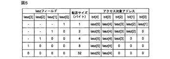
laszフィールドと、アクセス対象アドレスの下位ビットおよび転送サイズの関係を、図面を参照して説明する。 The relationship between the lasz field, the lower bits of the access target address, and the transfer size will be described with reference to the drawings.
図5は、laszフィールドと、アクセス対象アドレスの下位ビットおよび転送サイズの関係図である。 FIG. 5 is a diagram showing the relationship between the lasz field, the lower bits of the access target address, and the transfer size.
laszフィールドの最下位ビットの値が‘1’である場合、転送サイズは1バイトであり、アクセス対象アドレスのビット4からビット0まではlaszフィールドのビット5からビット1までである。
When the value of the least significant bit of the lasz field is “1”, the transfer size is 1 byte, and
laszフィールドの下位2ビットの値が“10”である場合、転送サイズは2バイトであり、アクセス対象アドレスのビット4からビット1まではlaszフィールドのビット5からビット2までであり、アクセス対象アドレスのビット0は‘0’である。
When the value of the lower 2 bits of the lasz field is “10”, the transfer size is 2 bytes,
laszフィールドの下位3ビットの値が“100”である場合、転送サイズは4バイトであり、アクセス対象アドレスのビット4からビット2まではlaszフィールドのビット5からビット3までであり、アクセス対象アドレスのビット1から0までは“00”である。
When the value of the lower 3 bits of the lasz field is “100”, the transfer size is 4 bytes,
laszフィールドの下位4ビットの値が“1000”である場合、転送サイズは8バイトであり、アクセス対象アドレスのビット4からビット3まではlaszフィールドのビット5からビット4までであり、アクセス対象アドレスのビット2からビット0までは“000”である。
When the value of the lower 4 bits of the lasz field is “1000”, the transfer size is 8 bytes,
laszフィールドの下位4ビットの値が“0000”である場合、転送サイズは32バイトであり、アクセス対象アドレスのビット4から3まではlaszフィールドのビット5からビット4までであり、アクセス対象アドレスのビット2から0は“000”までである。
When the value of the lower 4 bits of the lasz field is “0000”, the transfer size is 32 bytes,
uaddフィールドはアクセス対象アドレスの上位ビットを示す7ビットあるいは27ビットのフィールドである。uaddフィールドは、alenフィールドの値によってビット数が異なる。alenフィールドが‘0’であるとき、アドレス長は12ビットである。このとき、uaddフィールドは7ビットであり、アクセス対象アドレスのビット11からビット5までを示す。alenフィールドが‘1’であるとき、アドレス長は32ビットである。このとき、uaddフィールドは、27ビットであり、アクセス対象アドレスのビット31からビット5までを示す。
The uadd field is a 7-bit or 27-bit field indicating the upper bits of the access target address. The uadd field has a different number of bits depending on the value of the alen field. When the alen field is “0”, the address length is 12 bits. At this time, the uadd field has 7 bits and indicates
tidフィールドは、シリアルリクエストパケットとシリアルレスポンスパケットを対応付けるための3ビットのフィールドである。 The tid field is a 3-bit field for associating a serial request packet with a serial response packet.
本明細書のシリアルインタフェースは、パイプライン処理をサポートする。すなわち、イニシエータである集積回路A101は、送信したシリアルリクエストパケットに対するシリアルレスポンスパケットを受信する前に、前記シリアルリクエストパケットとは別のシリアルリクエストパケットを送信できる。ターゲットである集積回路B109は、受信したシリアルリクエストパケットに対するシリアルレスポンスパケットを送信する前に、前記シリアルリクエストパケットとは別のシリアルリクエストパケットを受信して処理することもできるが、シリアルリクエストパケットの受信順と、それらに対応するシリアルレスポンスパケットの送信順が同一であることを保証しない。ターゲットがシリアルレスポンスパケットの送信順を保証しない理由は、イニシエータのシリアルレスポンス受信待ち時間を短くするためである。例えば、シリアルレスポンスパケットの生成に時間がかかるシリアルリクエストパケットにつづいて、シリアルレスポンスパケットの生成に時間がかからないシリアルリクエストパケットを受信した場合、後に受信したシリアルリクエストパケットに対するシリアルレスポンスパケットを、先に受信したシリアルリクエストパケットに対するシリアルレスポンスパケットよりも先に送信することによって、イニシエータのシリアルレスポンスパケット受信待ち時間を短くすることができる。 The serial interface herein supports pipeline processing. That is, the integrated circuit A101, which is an initiator, can transmit a serial request packet different from the serial request packet before receiving a serial response packet for the transmitted serial request packet. The target integrated circuit B109 can receive and process a serial request packet different from the serial request packet before transmitting a serial response packet for the received serial request packet. It is not guaranteed that the order and the transmission order of the corresponding serial response packets are the same. The reason why the target does not guarantee the transmission order of the serial response packet is to shorten the serial response reception waiting time of the initiator. For example, when a serial request packet that takes a long time to generate a serial response packet is received, and a serial request packet that does not take a long time to generate a serial response packet is received, the serial response packet for the serial request packet received later is received first. By transmitting before the serial response packet for the serial request packet, the serial response packet reception waiting time of the initiator can be shortened.
集積回路B109は、シリアルリクエストパケット受信時にtidフィールドの値を保存し、対応するシリアルレスポンスパケットを送信する際にr_tidフィールド(後述)として出力する。集積回路A101は、r_tidフィールドによってシリアルリクエストパケットとシリアルレスポンスパケットを対応付ける。
The
wdataフィールドは、集積回路A101から集積回路B109に転送されるライトデータを含むフィールドである。wdataフィールドは、ライトアクセスのシリアルリクエストパケットのみに存在し、リードアクセスのシリアルリクエストパケットには存在しない。 The wdata field is a field including write data transferred from the integrated circuit A101 to the integrated circuit B109. The wdata field exists only in the serial request packet for write access and does not exist in the serial request packet for read access.
つづいて、シリアルレスポンスパケットのフォーマットを図面を参照して説明する。 Next, the format of the serial response packet will be described with reference to the drawings.
図6は、シリアルレスポンスパケットフォーマットを示す図である。シリアルレスポンスパケットは、start、basic、reqrsp、dss、r_sid、r_tid、rdataの各フィールドを含む。 FIG. 6 is a diagram showing a serial response packet format. The serial response packet includes fields of start, basic, reqrsp, dss, r_sid, r_tid, and rdata.
startフィールドは、シリアルパケットの先頭ビットの位置を示す1ビットのフィールドである。startフィールドが‘1’である位置が、シリアルパケットの先頭である。 The start field is a 1-bit field indicating the position of the first bit of the serial packet. The position where the start field is “1” is the head of the serial packet.
basicフィールドは、シリアルパケットの種類を示す1ビットのフィールドである。basicフィールドが‘1’であるパケットは、シリアルリクエストパケットあるいはシリアルレスポンスパケットであり、basicフィールドが‘0’であるパケットは、シリアルコントロールパケットである。 The basic field is a 1-bit field indicating the type of serial packet. A packet whose basic field is “1” is a serial request packet or a serial response packet, and a packet whose basic field is “0” is a serial control packet.
reqrspは、パケットがリクエストパケットであるかレスポンスパケットであるかを示す1ビットのフィールドである。reqrspフィールドが‘0’であるパケットがレスポンスパケットである。 reqrsp is a 1-bit field indicating whether the packet is a request packet or a response packet. A packet whose reqrsp field is “0” is a response packet.
dssフィールドは、アクセスの成否とシリアルレスポンスパケットに含まれるリードデータの量を示す3ビットのフィールドである。dssフィールドの値と、アクセス成否およびリードデータ量の関係を図面を参照して説明する。 The dss field is a 3-bit field indicating the success or failure of access and the amount of read data included in the serial response packet. The relationship between the value of the dss field, access success / failure, and read data amount will be described with reference to the drawings.
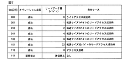
図7は、dssフィールドの値と、アクセス成否およびリードデータ量の関係を示す関係図である。 FIG. 7 is a relationship diagram showing the relationship between the value of the dss field, access success / failure, and read data amount.
dssフィールドの値が“000”であるとき、シリアルレスポンスパケットに含まれるリードデータの量は0バイトであり、アクセスは成功である。すなわち、“000”は、ライトアクセスに成功したときのdssフィールドの値である。 When the value of the dss field is “000”, the amount of read data included in the serial response packet is 0 byte, and the access is successful. That is, “000” is the value of the dss field when the write access is successful.
dssフィールドの値が“001”であるとき、シリアルレスポンスパケットに含まれるリードデータの量は1バイトであり、アクセスは成功である。すなわち、“001”は、転送サイズ1バイトのリードアクセスに成功したときのdssフィールドの値である。 When the value of the dss field is “001”, the amount of read data included in the serial response packet is 1 byte, and the access is successful. That is, “001” is the value of the dss field when the read access with a transfer size of 1 byte is successful.
dssフィールドの値が“010”であるとき、シリアルレスポンスパケットに含まれるリードデータの量は2バイトであり、アクセスは成功である。すなわち、“010”は、転送サイズ2バイトのリードアクセスに成功したときのdssフィールドの値である。 When the value of the dss field is “010”, the amount of read data included in the serial response packet is 2 bytes, and the access is successful. That is, “010” is the value of the dss field when a read access with a transfer size of 2 bytes is successful.
dssフィールドの値が“011”であるとき、シリアルレスポンスパケットに含まれるリードデータの量は4バイトであり、アクセスは成功である。すなわち、“011”は、転送サイズ4バイトのリードアクセスに成功したときのdssフィールドの値である。 When the value of the dss field is “011”, the amount of read data included in the serial response packet is 4 bytes, and the access is successful. That is, “011” is the value of the dss field when a read access with a transfer size of 4 bytes is successful.
dssフィールドの値が“100”であるとき、シリアルレスポンスパケットに含まれるリードデータの量は8バイトであり、アクセスは成功である。すなわち、“100”は、転送サイズ8バイトのリードアクセスに成功したときのdssフィールドの値である。 When the value of the dss field is “100”, the amount of read data included in the serial response packet is 8 bytes, and the access is successful. That is, “100” is the value of the dss field when a read access with a transfer size of 8 bytes is successful.
dssフィールドの値が“101”であるとき、シリアルレスポンスパケットに含まれるリードデータの量は32バイトであり、アクセスは成功である。すなわち、“101”は、転送サイズ32バイトのリードアクセスに成功したときのdssフィールドの値である。 When the value of the dss field is “101”, the amount of read data included in the serial response packet is 32 bytes, and the access is successful. That is, “101” is the value of the dss field when read access with a transfer size of 32 bytes is successful.
dssフィールドの値が“110”であるとき、シリアルレスポンスパケットに含まれるリードデータの量は0バイトであり、アクセスは失敗である。すなわち、“110”は、リードアクセスあるいはライトアクセスに失敗したときのdssフィールドの値である。 When the value of the dss field is “110”, the amount of read data included in the serial response packet is 0 byte, and the access has failed. That is, “110” is the value of the dss field when read access or write access fails.
なお、ターゲットである集積回路B109がdssフィールドの値として“111”を出力することは、本明細書のシリアルインタフェースでは禁止されている。
Note that the output of “111” as the value of the dss field by the target integrated
r_sidフィールドは、シリアルリクエストパケットとシリアルレスポンスパケットを対応付けるための2ビットのフィールドである。ターゲットである集積回路B109は、シリアルリクエストパケット受信時にsidフィールドの値を保存し、対応するシリアルレスポンスパケットを送信する際にr_sidフィールドの値として出力する。イニシエータである集積回路A101はr_sidフィールドの値と後述するr_tidフィールドの値によって、シリアルリクエストパケットとシリアルレスポンスパケットの対応付けを行う。
The r_sid field is a 2-bit field for associating a serial request packet with a serial response packet. The target integrated
r_tidフィールドは、シリアルリクエストパケットとシリアルレスポンスパケットを対応付けるための3ビットのフィールドである。ターゲットである集積回路B109は、シリアルリクエストパケット受信時にtidフィールドの値を保存し、対応するシリアルレスポンスパケットを送信する際にr_tidフィールドの値として出力する。イニシエータである集積回路A101はr_tidフィールドの値とr_sidフィールドの値によって、シリアルリクエストパケットとシリアルレスポンスパケットの対応付けを行う。
The r_tid field is a 3-bit field for associating a serial request packet with a serial response packet. The target integrated
rdataフィールドは、ターゲットである集積回路B109からイニシエータである集積回路A101に転送されるデータである。シリアルレスポンスパケットにrdataフィールドが存在するのは、リードアクセスが成功した場合のみである。 The rdata field is data transferred from the target integrated circuit B109 to the initiator integrated circuit A101. The rdata field is present in the serial response packet only when the read access is successful.
つづいて、シリアルコントロールパケットのフォーマットを説明する。 Next, the format of the serial control packet will be described.
図8は、シリアルコントロールパケットのフォーマットを示す図である。シリアルコントロールパケットは、start、basic、reqrsp、reccc、intcodeの各フィールドを含む。 FIG. 8 is a diagram showing the format of the serial control packet. The serial control packet includes start, basic, reqrsp, reccc, and intcode fields.
startフィールドは、シリアルパケットの先頭ビットの位置を示す1ビットのフィールドである。startフィールドが‘1’である位置が、シリアルパケットの先頭である。 The start field is a 1-bit field indicating the position of the first bit of the serial packet. The position where the start field is “1” is the head of the serial packet.
basicフィールドは、シリアルパケットの種類を示す1ビットのフィールドである。basicフィールドが‘1’であるパケットは、シリアルリクエストパケットあるいはシリアルレスポンスパケットであり、basicフィールドが‘0’であるパケットは、シリアルコントロールパケットである。 The basic field is a 1-bit field indicating the type of serial packet. A packet whose basic field is “1” is a serial request packet or a serial response packet, and a packet whose basic field is “0” is a serial control packet.
reqrspは、パケットがリクエストパケットであるかレスポンスパケットであるかを示す1ビットのフィールドである。 reqrsp is a 1-bit field indicating whether the packet is a request packet or a response packet.
recccフィールドは、シリアルコントロールパケットの種類と割り込みレベルを示す7ビットのフィールドである。recccフィールドの上位3ビットはシリアルコントロールパケットの種類を示す。 The reccc field is a 7-bit field indicating the type of serial control packet and the interrupt level. The upper 3 bits of the reccc field indicate the type of serial control packet.
recccフィールドの上位3ビットが“100”であるシリアルコントロールパケットは、割り込み情報を含むシリアルコントロールパケットである。以下、本明細書では、割り込み情報を含むシリアルコントロールパケットを割り込みパケットという。 A serial control packet in which the upper 3 bits of the reccc field are “100” is a serial control packet including interrupt information. Hereinafter, in this specification, a serial control packet including interrupt information is referred to as an interrupt packet.
割り込みパケットにおいては、reqccフィールドの下位4ビットは割り込みレベルである。割り込みレベルは16段階であり、最も高い割り込みレベルではreqccフィールドの下位4ビットは“1111”であり、最も低い割り込みレベルではreqccフィールドの下位4ビットは“0000”である。なお、割り込みパケットはリクエストパケットのみであり、レスポンスパケットは存在しない。 In the interrupt packet, the lower 4 bits of the reqcc field are the interrupt level. The interrupt level has 16 stages. The lowest 4 bits of the reqcc field are “1111” at the highest interrupt level, and the lower 4 bits of the reqcc field are “0000” at the lowest interrupt level. The interrupt packet is only a request packet, and there is no response packet.
recccフィールドの上位3ビットが“000”であるシリアルコントロールパケットは、シリアルインタフェースのイニシエータを停止させるシリアルコントロールパケットである。以下、本明細書では、シリアルインタフェースのイニシエータを停止させるシリアルコントロールパケットをイニシエータストップパケットという。 The serial control packet in which the upper 3 bits of the reccc field are “000” is a serial control packet for stopping the initiator of the serial interface. Hereinafter, in this specification, the serial control packet for stopping the initiator of the serial interface is referred to as an initiator stop packet.
recccフィールドの上位3ビットが“001”であるシリアルコントロールパケットは、シリアルインタフェースのイニシエータの停止を解除するシリアルコントロールパケットである。以下、本明細書では、シリアルインタフェースのイニシエータの停止を解除するシリアルコントロールパケットをイニシエータストップ解除パケットという。 The serial control packet whose upper 3 bits of the reccc field are “001” is a serial control packet for canceling the stop of the initiator of the serial interface. Hereinafter, in this specification, the serial control packet for releasing the stop of the initiator of the serial interface is referred to as an initiator stop release packet.
intcodeフィールドは、割り込みパケットにのみ存在する16ビットのフィールドであり、割り込みの属性情報を含む。 The intcode field is a 16-bit field that exists only in the interrupt packet and includes interrupt attribute information.
ここで、シリアルインタフェースにおけるシリアルパケット転送の様子を図面を参照して説明する。 Here, the state of serial packet transfer in the serial interface will be described with reference to the drawings.
図9は、シリアルインタフェースにおけるシリアルリクエストパケットおよびシリアルコントロールパケットの転送の様子を示す図であり、図10はシリアルインタフェースにおけるシリアルレスポンスパケットの転送の様子を示す図である。本発明のシリアルインタフェースは、情報を送信する側が情報を示す信号とその情報のタイミングを示す信号を両方出力する、ソース同期式のインタフェースである。 FIG. 9 is a diagram showing how the serial request packet and serial control packet are transferred in the serial interface, and FIG. 10 is a diagram showing how the serial response packet is transferred in the serial interface. The serial interface of the present invention is a source-synchronous interface in which the information transmitting side outputs both a signal indicating information and a signal indicating the timing of the information.
シリアルリクエストパケットは、リクエストストローブの立ち上がりエッジに同期して転送される。リクエストストローブは、信号線群AB107のストローブ信号1201によって集積回路A101から集積回路B109に供給される。リクエストレーンにおいては、先に説明したシリアルリクエストパケットが、startフィールドから順に、かつリクエストレーンのMSB(Most Significant Bit)から順に転送される。図9においては、startフィールドを「0」で示している。startフィールドは必ずリクエストレーンのMSBを用いて転送される。このため、本発明のシリアルインタフェースにおいては、先に説明した集積回路A101におけるパラレルリクエストパケットの転送とは異なり、リクエストバリッド信号に相当する信号を必要としない。これはシリアルインタフェースの信号線数を少なくするためである。本発明のシリアルインタフェースのターゲットは、リクエストレーンのMSBを監視し、リクエストレーンのMSBが‘0’となった時刻からシリアルリクエストパケットあるいはシリアルコントロールパケットの受信を開始し、受信したシリアルパケットの内容を解析することにより該シリアルパケットの最終ビット(図9の「F」(Final)で示されたビット)および次のシリアルパケットの先頭位置を検出する。シリアルリクエストパケットやシリアルコントロールパケットのビット数がリクエストレーン数の倍数以外の場合には、リクエストレーンのMSB以外の信号線にダミーデータが出力される。
The serial request packet is transferred in synchronization with the rising edge of the request strobe. The request strobe is supplied from the integrated circuit A101 to the integrated circuit B109 by the
同様に、シリアルレスポンスパケットあるいはシリアルコントロールパケットは、startフィールドがレスポンスレーンのMSBによって転送され、以下、basic、reqrspの順にレスポンスレーンのMSB側を先にして順次転送される。 Similarly, the serial response packet or serial control packet is transferred by the MSB of the response lane in the start field, and is sequentially transferred in the order of basic and reqrsp, with the MSB side of the response lane first.
また、図9では一本のストローブ信号を用いたが、ストローブ信号として2本のLVDS(Low Voltage Differential Signaling)からなる信号群を用いることもできる。この場合、信号線数はシリアルインタフェース全体で2本増加するが、他の信号の倍の頻度で変化するストローブ信号が低振幅化され、動作周波数上限が高めやすくなる。たとえば、LVDS信号でストローブを伝送するDDR2―SDRAMコントローラの物理層回路を本発明のシリアルインタフェースの物理層回路として用いれば、リクエストレーンあるいはレスポンスレーンの信号線一本あたりのデータレートを毎秒800メガビットまで容易に高めることができる。この場合、本実施の形態におけるシリアルインタフェースの転送スループットは、リクエストレーンとレスポンスレーンの合計で毎秒600メガバイトとなる。 Further, although one strobe signal is used in FIG. 9, a signal group including two LVDS (Low Voltage Differential Signaling) can be used as the strobe signal. In this case, the number of signal lines is increased by two over the entire serial interface, but the strobe signal that changes at twice the frequency of the other signals is reduced in amplitude, and the upper limit of the operating frequency is easily increased. For example, if the physical layer circuit of the DDR2-SDRAM controller that transmits the strobe with the LVDS signal is used as the physical layer circuit of the serial interface of the present invention, the data rate per signal line of the request lane or response lane is up to 800 megabits per second. Can be easily increased. In this case, the transfer throughput of the serial interface in this embodiment is 600 megabytes per second in total for the request lane and the response lane.
集積回路A101の説明に戻る。集積回路A101に含まれるイニシエータA105について図面を参照して説明する。 Returning to the description of the integrated circuit A101. The initiator A105 included in the integrated circuit A101 will be described with reference to the drawings.
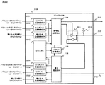
図11は、イニシエータA105の構成を示すブロック図である。
FIG. 11 is a block diagram showing the configuration of the
イニシエータA105は、リクエスト送信制御部A1101と、レスポンス受信制御部A1102と、割り込み受信制御部A1103と、暗号化送信部A1104と、パケット計数部A1105と、復号受信部A1106と、レジスタA1107と、3ステートバッファ201と、プルアップ抵抗203とを備えて構成される。
The initiator A105 includes a request transmission control unit A1101, a response reception control unit A1102, an interrupt reception control unit A1103, an encrypted transmission unit A1104, a packet counting unit A1105, a decryption reception unit A1106, a register A1107, and three states. A
リクエスト送信制御部A1101は、ルータA106からパラレルリクエストパケットを受信し、該パラレルリクエストパケットのアドレスがレジスタA1107を示すときには該パラレルリクエストパケットをレジスタA1107に送信し、該パラレルリクエストパケットのアドレスがレジスタA1107を示さないときには該パラレルリクエストパケットを暗号化送信部A1104に送信する中継回路である。 The request transmission control unit A1101 receives the parallel request packet from the router A106, and transmits the parallel request packet to the register A1107 when the address of the parallel request packet indicates the register A1107. The address of the parallel request packet stores the register A1107. When not shown, the relay circuit transmits the parallel request packet to the encrypted transmission unit A1104.
レスポンス受信制御部A1102は、復号受信部A1106およびレジスタA1107からパラレルレスポンスパケットを受信し、該パラレルレスポンスパケットをルータA106に送信する中継回路である。 The response reception control unit A1102 is a relay circuit that receives parallel response packets from the decoding reception unit A1106 and the register A1107 and transmits the parallel response packets to the router A106.
割り込み受信制御部A1103は、復号受信部A1106から割り込みパケットを受信して該割り込みパケットの内容を解析し、解析結果に基づいてINTCA104に対する割り込み信号を生成する割り込み情報中継回路である。
The interrupt reception control unit A1103 is an interrupt information relay circuit that receives an interrupt packet from the decoding reception unit A1106, analyzes the content of the interrupt packet, and generates an interrupt signal for the
暗号化送信部A1104は、リクエスト送信制御部A1101からパラレルリクエストパケットを受信し、該パラレルリクエストパケットをシリアルリクエストパケットに変換し、さらに該シリアルリクエストパケットを暗号化して信号線群AB107を介して集積回路B109に送信する中継回路である。暗号化送信部A1104はシリアルリクエストパケットを中継するときに、合わせて以下の処理を行う。暗号化送信部A1104は、パケット計数部A1105から供給されるシリアルリクエストパケット送信許可信号がディアサート状態であるときには、集積回路B109へのシリアルリクエストパケット送信を行わない。暗号化送信部A1104は、集積回路B109へのシリアルリクエストパケット送信が完了するたびに、シリアルリクエストパケットの送信が完了した旨と、送信したシリアルリクエストパケットのrwフィールドの値を、パケット計数部A1105に通知する。暗号化送信部A1104は、後述のリクエストレーン数レジスタAを参照し、該レジスタの値によって指定された数の信号線群AB107に含まれる情報信号線群を用いてシリアルリクエストパケットを送信する。暗号化送信部A1104は、後述の暗号機能イネーブルレジスタAの値と暗号化暗号鍵レジスタAの値をそれぞれ参照し、該暗号機能イネーブルレジスタAの値が暗号化機能が有効であることを示す値である場合には、該暗号化暗号鍵レジスタAによって指定された暗号鍵を用いてシリアルリクエストパケットの暗号化を行う。 The encrypted transmission unit A1104 receives the parallel request packet from the request transmission control unit A1101, converts the parallel request packet into a serial request packet, further encrypts the serial request packet, and integrates the integrated circuit via the signal line group AB107. This is a relay circuit for transmitting to B109. When the encrypted transmission unit A1104 relays the serial request packet, the encrypted transmission unit A1104 also performs the following processing. The encrypted transmission unit A1104 does not transmit the serial request packet to the integrated circuit B109 when the serial request packet transmission permission signal supplied from the packet counting unit A1105 is in the deasserted state. Each time the serial request packet transmission to the integrated circuit B109 is completed, the encrypted transmission unit A1104 notifies the packet counting unit A1105 of the completion of transmission of the serial request packet and the value of the rw field of the transmitted serial request packet. Notice. The encryption transmission unit A1104 refers to a request lane number register A, which will be described later, and transmits a serial request packet using information signal line groups included in the number of signal line groups AB107 designated by the value of the register. The encryption transmission unit A1104 refers to the value of the encryption function enable register A and the value of the encryption encryption key register A described later, and the value of the encryption function enable register A indicates that the encryption function is valid. If it is, the serial request packet is encrypted using the encryption key specified by the encryption encryption key register A.
パケット計数部A1105は、アウトスタンディングカウンタ、リードアウトスタンディングカウンタ、ライトアウトスタンディングカウンタを備える。 The packet counting unit A1105 includes an standing counter, a lead-out standing counter, and a write-out standing counter.
アウトスタンディングカウンタは、暗号化送信部A1105からシリアルリクエストパケットの送信が完了したことを通知されるたびにカウント値を1増加させ、復号受信部A1106からシリアルレスポンスパケットの受信が完了したことを通知されるたびにカウント値を1減少させる。ただし、アウトスタンディングカウンタはシリアルリクエストパケット送信とシリアルレスポンスパケット受信が同時に完了したときにはカウント値を変化させない。また、アウトスタンディングカウンタは、集積回路A101の初期化時に0となる。 The outstanding counter increments the count value by 1 every time the transmission of the serial request packet is notified from the encryption transmission unit A1105, and is notified that the reception of the serial response packet is completed from the decryption reception unit A1106. Each time, the count value is decreased by one. However, the standing counter does not change the count value when the serial request packet transmission and the serial response packet reception are completed at the same time. In addition, the outstanding counter becomes 0 when the integrated circuit A101 is initialized.
リードアウトスタンディングカウンタは、暗号化送信部A1105からrwフィールドが‘1’であるシリアルリクエストパケットの送信が完了したことを通知されるたびにカウント値を1増加させ、復号受信部A1106から前記シリアルリクエストパケットに対応するシリアルレスポンスパケットの受信が完了したことを通知されるたびにカウント値を1減少させる。ただし、リードアウトスタンディングカウンタはrwフィールドが‘1’であるシリアルリクエストパケットの送信と該シリアルリクエストパケットに対応するシリアルレスポンスパケットの受信が同時に行われたときにはカウント値を変化させない。また、リードアウトスタンディングカウンタは、集積回路A101の初期化時に0となる。 The lead-out standing counter increments the count value by 1 every time it is notified from the encrypted transmission unit A1105 that transmission of the serial request packet whose rw field is “1” is completed, and the serial request is received from the decryption reception unit A1106. Every time it is notified that the reception of the serial response packet corresponding to the packet is completed, the count value is decreased by one. However, the lead-out standing counter does not change the count value when a serial request packet whose rw field is “1” and a serial response packet corresponding to the serial request packet are simultaneously received. The lead-out standing counter becomes 0 when the integrated circuit A101 is initialized.
ライトアウトスタンディングカウンタは、暗号化送信部A1105からrwフィールドが‘0’であるシリアルリクエストパケットの送信が完了したことを通知されるたびにカウント値を1増加させ、復号受信部A1106から前記シリアルリクエストパケットに対応するシリアルレスポンスパケットの受信が完了したことを通知されるたびにカウント値を1減少させる。ただし、ライトアウトスタンディングカウンタは、rwフィールドが‘1’であるシリアルリクエストパケット送信と該シリアルリクエストパケットに対応するシリアルレスポンスパケットの受信が同時に行われたときにはカウント値を変化させない。また、ライトアウトスタンディングカウンタは、集積回路A101の初期化時に0となる。 The write-out standing counter increments the count value by 1 every time when the transmission of the serial request packet whose rw field is “0” is notified from the encryption transmission unit A1105, and the serial request is received from the decryption reception unit A1106. Every time it is notified that the reception of the serial response packet corresponding to the packet is completed, the count value is decreased by one. However, the write-out standing counter does not change the count value when the serial request packet transmission in which the rw field is “1” and the serial response packet corresponding to the serial request packet are simultaneously received. The write-out standing counter becomes 0 when the integrated circuit A101 is initialized.
パケット計数部A1105は、後述の最大アウトスタンディングレジスタAの値と、後述の最大リードアウトスタンディングレジスタAの値と、後述の最大ライトアウトスタンディングレジスタAの値を参照する。パケット計数部A1105は、該最大アウトスタンディングレジスタAの値が前記アウトスタンディングカウンタの値より大きく、かつ、該最大リードアウトスタンディングレジスタAの値が前記リードアウトスタンディングカウンタの値より大きく、かつ、該最大ライトアウトスタンディングレジスタAの値が前記ライトアウトスタンディングカウンタの値より大きいときに、暗号化送信部A1105に対するシリアルリクエストパケット送信許可信号をアサート状態に保持する。
The packet counting unit A1105 refers to the value of the maximum outstanding register A described later, the value of the maximum read outstanding register A described later, and the value of the maximum write outstanding register A described later. The packet counting unit A1105 has a value of the maximum outstanding register A larger than a value of the outstanding counter, a value of the maximum read outstanding register A is larger than a value of the read outstanding counter, and the maximum When the value of the write-out standing register A is larger than the value of the write-out standing counter, the serial request packet transmission permission signal for the encrypted
復号受信部A1106は、信号線群BA108を介して集積回路B109からシリアルパケットを受信し、レスポンス受信制御部A1102あるいは割り込み受信制御部A1103に送信する中継回路である。復号受信部A1106は、シリアルパケットを中継するときに、合わせて以下の処理を行う。復号受信部A1106は、後述のレスポンスレーン数レジスタAの値を参照し、該レジスタによって指定された数の信号線群BA108に含まれる情報信号群を用いて、シリアルパケットを受信する。復号受信部A1106は、集積回路B109から受信したシリアルパケットの内容を解析し、該シリアルパケットがシリアルレスポンスパケットであるか割り込みパケットであるかを判断する。復号受信部A1106は、受信したシリアルパケットがシリアルレスポンスパケットである場合には、パラレルレスポンスパケットに変換し、該パラレルレスポンスパケットをレスポンス受信制御部A1102に送信する。このとき、復号受信部A1106は、後述の暗号機能イネーブルレジスタAと後述の復号暗号鍵レジスタAの値をそれぞれ参照し、該暗号機能イネーブルレジスタAの値が暗号化機能が有効であることを示す値である場合には、前記レジスタAによって指定された暗号鍵を用いて復号を行う。
The decoding reception unit A1106 is a relay circuit that receives a serial packet from the integrated circuit B109 via the signal line group BA108 and transmits it to the response reception control unit A1102 or the interrupt reception control unit A1103. The decoding reception unit A1106 performs the following processing together when relaying the serial packet. The decoding reception unit A1106 refers to a value of a response lane number register A described later, and receives a serial packet by using the information signal group included in the number of signal line groups BA108 specified by the register. The decoding reception unit A1106 analyzes the content of the serial packet received from the integrated circuit B109, and determines whether the serial packet is a serial response packet or an interrupt packet. When the received serial packet is a serial response packet, the decoding reception unit A1106 converts the received serial packet into a parallel response packet and transmits the parallel response packet to the response reception control unit A1102. At this time, the decryption receiving
復号受信部A1106は、受信したシリアルパケットが割り込みパケットであると判断した場合には、該割り込みパケットを割り込み受信制御部A1103に送信する。 When the decoding reception unit A1106 determines that the received serial packet is an interrupt packet, the decoding reception unit A1106 transmits the interrupt packet to the interrupt reception control unit A1103.
レジスタA1107は、集積回路A101がシリアルインタフェースによって集積回路B109との間で通信を行うために必要な制御情報を保持するための記憶装置である。レジスタA1107は、リクエスト送信制御部A1101から受信したパラレルリクエストパケットを解析し、解析結果に基づいて後述する各レジスタに対する処理を行い、処理結果に基づいてパラレルレスポンスパケットを生成し、該パラレルレスポンスパケットを暗号化送信部A1102に送信する。 The register A1107 is a storage device for holding control information necessary for the integrated circuit A101 to communicate with the integrated circuit B109 through a serial interface. The register A1107 analyzes the parallel request packet received from the request transmission control unit A1101, performs processing for each register described later based on the analysis result, generates a parallel response packet based on the processing result, and outputs the parallel response packet. The data is transmitted to the encrypted transmission unit A1102.
つづいて、図面を参照してレジスタA1107に含まれるレジスタ群を説明する。図12はレジスタA1107に含まれるレジスタ群を示す図である。
Next, a register group included in the
レジスタA1107は、最大アウトスタンディングレジスタA、最大リードアウトスタンディングレジスタA、最大ライトアウトスタンディングレジスタA、暗号機能イネーブルレジスタA、暗号化暗号鍵レジスタA、復号暗号鍵レジスタA、リクエストレーン数レジスタA、レスポンスレーン数レジスタAを備えて構成される。
最大アウトスタンディングレジスタAは、イニシエータA105の最大アウトスタンディング数が保持されるレジスタである。最大アウトスタンディングレジスタAの値は、集積回路A101の初期化時に1となり、CPUA102によるライトアクセスによって値が更新される。 The maximum outstanding register A is a register that holds the maximum outstanding number of the initiator A105. The value of the maximum outstanding register A becomes 1 when the integrated circuit A101 is initialized, and the value is updated by the write access by the CPU A102.
最大リードアウトスタンディングレジスタAは、イニシエータA105のリードアクセスの最大アウトスタンディング数が保持されるレジスタである。最大リードアウトスタンディングレジスタAの値は、集積回路A101の初期化時に1となり、CPUA102によるライトアクセスによって値が更新される。
The maximum lead-out standing register A is a register that holds the maximum number of stand-outs for the read access of the
最大ライトアウトスタンディングレジスタAは、イニシエータA105のライトアクセスの最大アウトスタンディング数が保持されるレジスタである。最大ライトアウトスタンディングレジスタAの値は、集積回路A101の初期化時に1となり、CPUA102によるライトアクセスによって値が更新される。
The maximum write-out standing register A is a register that holds the maximum number of write access outstanding of the
暗号機能イネーブルレジスタAは、イニシエータA105が送受信するシリアルリクエストパケットとシリアルレスポンスパケットが、暗号化されるか否かを設定するレジスタである。暗号機能イネーブルレジスタAの値が‘1’である場合、暗号化機能は有効であり、シリアルリクエストパケットおよびシリアルレスポンスパケットはそれぞれシリアルインタフェース上を暗号化された状態で送受信される。
The encryption function enable register A is a register for setting whether or not the serial request packet and serial response packet transmitted / received by the
復号暗号鍵レジスタAは、復号受信部A1106が暗号を復号するときに使用する暗号鍵が保持されるレジスタである。暗号化暗号鍵レジスタAは、暗号化送信部A1104がシリアルリクエストパケットを暗号化するときに使用する暗号鍵が保持されるレジスタである。 The decryption encryption key register A is a register that holds an encryption key used when the decryption receiving unit A1106 decrypts the encryption. The encryption encryption key register A is a register that holds an encryption key used when the encryption transmission unit A1104 encrypts the serial request packet.
リクエストレーン数レジスタAは、信号線群AB107に含まれる情報信号線群の本数を示すレジスタである。リクエストレーン数レジスタAの値は、集積回路A101の初期化時に1となり、CPUA102によるライトアクセスによって更新される。レスポンスレーン数レジスタAは、信号線群BA108に含まれる情報信号線群の本数を示すレジスタである。レスポンスレーン数レジスタの値は、集積回路A101の初期化時に1となり、CPUA102によるライトアクセスによって更新される。 The request lane number register A is a register indicating the number of information signal line groups included in the signal line group AB107. The value of the request lane number register A becomes 1 when the integrated circuit A101 is initialized, and is updated by a write access by the CPU A102. The response lane number register A is a register indicating the number of information signal line groups included in the signal line group BA108. The value of the response lane number register becomes 1 when the integrated circuit A101 is initialized, and is updated by a write access by the CPU A102.
続いて、ターゲットB112の構成について図面を参照して説明する。 Next, the configuration of the target B112 will be described with reference to the drawings.
図13は、ターゲットB112の構成を示すブロック図である。 FIG. 13 is a block diagram showing the configuration of the target B112.
ターゲットB112は、復号受信部B1301と、暗号化送信部B1302と、リクエスト受信制御部B1303と、レジスタB1304と、レスポンス送信制御部B1305と、割り込み送信制御部B1306と、3ステートバッファ202とを備えて構成される。
The target B112 includes a decryption reception unit B1301, an encryption transmission unit B1302, a request reception control unit B1303, a register B1304, a response transmission control unit B1305, an interrupt transmission control unit B1306, and a three-
復号受信部B1301は、後述のリクエストレーン数レジスタBの値を参照し、該レジスタによって指定された数の信号線群AB107に含まれる情報信号群を介して集積回路A101からシリアルリクエストパケットを受信する受信回路であり、受信したシリアルリクエストパケットをパラレルリクエストパケットに変換した上で、さらに以下の処理を行う。復号受信部B1301は、後述の暗号機能イネーブルレジスタBと後述の復号暗号鍵レジスタBの値をそれぞれ参照し、該暗号機能イネーブルレジスタBの値が暗号化機能が有効であることを示す値である場合には、前記レジスタBによって指定された暗号鍵を用いてシリアルリクエストパケットの復号を行う。復号受信部B1301は、該パラレルリクエストパケットの内容を解析し、該パラレルリクエストパケットがレジスタB1304に対するアクセス要求を含むパラレルリクエストパケットであるか、メモリB110やIPB111に対するアクセス要求を含むパラレルリクエストパケットであるかを判断する。復号受信部B1301は、該パラレルリクエストパケットがレジスタB1304に対するアクセス要求を含むパラレルリクエストパケットであれば、該パラレルリクエストパケットをレジスタB1304に送信し、該パラレルリクエストパケットがメモリB110やIPB111に対するアクセス要求を含むパラレルリクエストパケットであれば、該パラレルリクエストパケットをルータB113に送信する。
The decoding reception unit B1301 refers to a value of a request lane number register B described later, and receives a serial request packet from the integrated circuit A101 via the information signal group included in the number of signal line groups AB107 specified by the register. The receiving circuit converts the received serial request packet into a parallel request packet, and further performs the following processing. The decryption receiving unit B1301 refers to values of a later-described encryption function enable register B and a later-described decryption encryption key register B, and the value of the encryption function enable register B is a value indicating that the encryption function is valid. In this case, the serial request packet is decrypted using the encryption key designated by the register B. The decoding reception unit B1301 analyzes the contents of the parallel request packet, and determines whether the parallel request packet is a parallel request packet including an access request for the register B1304 or a parallel request packet including an access request for the memory B110 or the
リクエスト受信制御部B1303は、復号受信部B1301からパラレルリクエストパケットを受信し、該パラレルリクエストパケットをルータB113に送信する中継回路である。 The request reception control unit B1303 is a relay circuit that receives a parallel request packet from the decoding reception unit B1301 and transmits the parallel request packet to the router B113.
レジスタB1304は、集積回路B109がシリアルインタフェースによって集積回路A101と通信するために必要な制御情報を保持する記憶装置である。レジスタB1304は、リクエスト受信制御部B1303から受信したパラレルリクエストパケットに基づいて後述するレジスタ群にアクセスし、アクセスに基づいてパラレルレスポンスパケットを生成し、該パラレルレスポンスパケットをレスポンス送信制御部B1305に送信する記憶装置である。 The register B1304 is a storage device that holds control information necessary for the integrated circuit B109 to communicate with the integrated circuit A101 through a serial interface. The register B1304 accesses a later-described register group based on the parallel request packet received from the request reception control unit B1303, generates a parallel response packet based on the access, and transmits the parallel response packet to the response transmission control unit B1305. It is a storage device.
つづいて、図14を用いてレジスタB1304に含まれるレジスタ群について説明する。
Next, a register group included in the
図14は、レジスタB1304に含まれるレジスタ群を示す図である。レジスタB1304は、最大アウトスタンディングレジスタB、最大リードアウトスタンディングレジスタB、最大ライトアウトスタンディングレジスタB、暗号機能イネーブルレジスタB、復号暗号鍵レジスタB、暗号化暗号鍵レジスタB、リクエストレーン数レジスタB、レスポンスレーン数レジスタB、モジュール電力制御レジスタB、モジュールクロック制御レジスタB、割り込み送信イネーブルレジスタBを備えて構成される。
FIG. 14 is a diagram illustrating a register group included in the
最大アウトスタンディングレジスタBは、ターゲットB112が対応可能な最大アウトスタンディング数が保持されるレジスタである。最大アウトスタンディングレジスタBの値は、集積回路B109の初期化時に4となり、ライトアクセスによって更新される。ただし、該ライトアクセスのライトデータの値が5以上である場合には、最大アウトスタンディングレジスタBの値は更新されず、暗号化送信部B1302にはアクセス失敗が通知される。
The maximum outstanding register B is a register that holds the maximum number of outstandings that can be handled by the
最大リードアウトスタンディングレジスタBは、ターゲットB112が対応可能なリードアクセスの最大アウトスタンディング数が保持されるレジスタである。最大リードアウトスタンディングレジスタBの値は、集積回路B109の初期化時に2となり、ライトアクセスによって更新される。ただし、該ライトアクセスのライトデータの値が3以上である場合には、最大リードアウトスタンディングレジスタBの値は更新されず、暗号化送信部B1302にはアクセス失敗が通知される。
The maximum lead-out standing register B is a register that holds the maximum number of read accesses that can be handled by the
最大ライトアウトスタンディングレジスタBは、ターゲットB112が対応可能なライトアクセスの最大アウトスタンディング数が保持されるレジスタである。最大ライトアウトスタンディングレジスタBの値は、集積回路B105の初期化時に2となり、ライトアクセスによって値が更新される。ただし、該ライトアクセスのライトデータの値が3以上である場合には、最大ライトアウトスタンディングレジスタBの値は更新されず、暗号化送信部B1302にはアクセス失敗が通知される。
The maximum write-out standing register B is a register that holds the maximum number of write access outstanding that the
暗号機能イネーブルレジスタBは、ターゲットB112が送受信するシリアルリクエストパケットおよびシリアルレスポンスパケットが暗号化されるか否かが設定されるレジスタである。暗号機能イネーブルレジスタBの値が‘1’である場合、シリアルリクエストパケットおよびシリアルレスポンスパケットはそれぞれシリアルインタフェースを暗号化された状態で送受信される。
The encryption function enable register B is a register for setting whether or not the serial request packet and serial response packet transmitted / received by the
復号暗号鍵レジスタBは、復号受信部B1301がシリアルリクエストパケットを復号するときに使用する暗号鍵が保持されるレジスタである。暗号化暗号鍵レジスタBは、暗号化送信部B1302がシリアルレスポンスパケットを暗号化するときに使用する暗号鍵が保持されるレジスタである。
The decryption encryption key register B is a register that holds an encryption key used when the decryption receiving unit B1301 decrypts the serial request packet. The encryption encryption key register B is a register that holds an encryption key used when the encryption
リクエストレーン数レジスタBは、信号線群AB107に含まれる情報信号線群の本数を示すレジスタである。リクエストレーン数レジスタBの値は、集積回路B109の初期化時に1となり、ライトアクセスによって更新される。レスポンスレーン数レジスタBは、信号線群BA108に含まれる情報信号線群の本数を示すレジスタである。レスポンスレーン数レジスタBの値は、集積回路B109の初期化時に1となり、ライトアクセスによって更新される。
The request lane number register B is a register indicating the number of information signal line groups included in the signal line group AB107. The value of the request lane number register B becomes 1 when the
モジュール電力制御レジスタBは、IPB111に電力供給を行うか否かを示すレジスタである。モジュール電力制御レジスタBの値が‘1’である場合、電力制御部B114に対する電力供給信号がアサート状態に保持され、モジュール電力制御レジスタBの値が‘0’である場合、電力制御部B114に対する電力供給信号がディアサート状態に保持される。モジュール電力制御レジスタBの値は、集積回路B109の初期化時に1となり、ライトアクセスによって更新される。
The module power control register B is a register that indicates whether or not to supply power to the
モジュールクロック制御レジスタBは、IPB111にクロック供給を行うか否かを示すレジスタである。モジュールクロック制御レジスタBの値が‘1’である場合、クロック制御部B115に対するクロック供給信号がアサート状態に保持され、モジュールクロック制御レジスタBの値が‘0’である場合、クロック制御部B115に対するクロック供給信号がディアサート状態に保持される。モジュールクロック制御レジスタBの値は、集積回路B109の初期化時に1となり、ライトアクセスによって更新される。
The module clock control register B is a register indicating whether or not to supply a clock to the
割り込み送信イネーブルレジスタBは、集積回路A101への割り込みパケット送信が許可されているか否かを示すレジスタである。割り込み送信イネーブルレジスタBの値が‘0’である場合、集積回路A101への割り込みパケット送信は禁止であり、割り込み送信イネーブルレジスタBの値が‘1’である場合、集積回路A101への割り込みパケット送信は許可されている。割り込み送信イネーブルレジスタBの値は、集積回路B109の初期化時に‘0’となり、ライトアクセスによって更新される。 The interrupt transmission enable register B is a register that indicates whether or not interrupt packet transmission to the integrated circuit A101 is permitted. When the value of the interrupt transmission enable register B is “0”, interrupt packet transmission to the integrated circuit A101 is prohibited, and when the value of the interrupt transmission enable register B is “1”, the interrupt packet to the integrated circuit A101 is Transmission is permitted. The value of the interrupt transmission enable register B becomes “0” when the integrated circuit B109 is initialized, and is updated by write access.
レスポンス送信制御部B1305は、ルータB113からパラレルレスポンスパケットを受信し、該パラレルレスポンスパケットを暗号化送信部B1305に送信する中継回路である。 The response transmission control unit B1305 is a relay circuit that receives a parallel response packet from the router B113 and transmits the parallel response packet to the encrypted transmission unit B1305.
割り込み送信制御部B1306は、IPB111から割り込み送信要求を取り込み、該割り込み送信要求に基づいて割り込みパケットを生成し、該割り込みパケットを暗号化送信部B1302に送信する割り込み中継回路である。
The interrupt transmission control unit B1306 is an interrupt relay circuit that takes in an interrupt transmission request from the
ターゲットB112の構成要素の説明に戻る。 Returning to the description of the components of the target B112.
暗号化送信部B1302は、レジスタB1304およびレスポンス送信制御部B1305からパラレルレスポンスパケットを、割り込み送信制御部B1306から割り込みパケットを受信し、受信したパケットをシリアルパケットに変換して信号線群BA108を介して集積回路A101に送信する中継回路であり、合わせて以下の処理を行う。 The encrypted transmission unit B1302 receives the parallel response packet from the register B1304 and the response transmission control unit B1305, receives the interrupt packet from the interrupt transmission control unit B1306, converts the received packet into a serial packet, and transmits the packet via the signal line group BA108. This is a relay circuit that transmits to the integrated circuit A101, and performs the following processing together.
暗号化送信部B1302は、レスポンスレーン数レジスタBを参照し、該レジスタの値によって指定された数の信号線群BA108に含まれる情報信号線群を用いてシリアルレスポンスパケットを送信する。暗号化送信部B1302は、暗号機能イネーブルレジスタBの値と暗号化暗号鍵レジスタBの値をそれぞれ参照し、該暗号機能イネーブルレジスタBの値が暗号化機能が有効であることを示す値である場合には、該暗号化暗号鍵レジスタBによって指定された暗号鍵を用いてシリアルレスポンスパケットの暗号化を行う。暗号化送信部B1302は、割り込み送信イネーブルレジスタBの値を参照し、該レジスタの値が割り込みパケット送信を許可しない値であるときには、割り込みパケット送信を行わない。
The encrypted
以下、本発明によるシリアルインタフェースを用いて、集積回路A101と集積回路B109の間で実行されるアクセスと、割り込み処理について説明する。
Hereinafter, access and interrupt processing executed between the
まず、シリアルインタフェースの初期設定を図面を参照して説明する。 First, the initial setting of the serial interface will be described with reference to the drawings.
図15は、集積回路A101および集積回路B109の使用開始から、シリアルインタフェースの初期化完了までの一連の初期設定処理を示すフローチャートである。集積回路A101および集積回路B109の使用開始時には、集積回路A101および集積回路B109に電力を供給し(ステップ1501)、つづいてリセット信号などを用いて回路の初期化を行う(ステップ1502)。 FIG. 15 is a flowchart showing a series of initial setting processes from the start of use of the integrated circuit A101 and the integrated circuit B109 to the completion of initialization of the serial interface. At the start of use of the integrated circuit A101 and the integrated circuit B109, power is supplied to the integrated circuit A101 and the integrated circuit B109 (step 1501), and then the circuit is initialized using a reset signal or the like (step 1502).
ステップ1502完了時におけるレジスタA1107およびレジスタB1304に含まれる各レジスタの値を図16に示す。図16は、初期化完了時のレジスタA1107およびレジスタB1304に含まれる各レジスタの値である。
FIG. 16 shows the values of the registers included in the
最大アウトスタンディングレジスタA、最大リードアウトスタンディングレジスタAおよび最大ライトアウトスタンディングレジスタAの各値は1であり、集積回路A101がリードアクセスあるいはライトアクセスを最大アウトスタンディング数1で実行することを示している。一方、最大アウトスタンディングレジスタB、最大リードアウトスタンディングレジスタB、最大ライトアウトスタンディングレジスタBの各値は1であり、集積回路B109がリードアクセスあるいはライトアクセスを最大アウトスタンディング数1で受け付けることを示している。
Each value of the maximum outstanding register A, the maximum read out standing register A, and the maximum write out standing register A is 1, indicating that the integrated circuit A101 executes read access or write access with the maximum number of
暗号機能イネーブルレジスタAおよび暗号機能イネーブルレジスタBの値は、それぞれパケットが暗号化されないことを示す‘0’である。 The values of the encryption function enable register A and the encryption function enable register B are “0” indicating that the packet is not encrypted.
リクエストレーン数レジスタAおよびリクエストレーン数レジスタBは、いずれもリクエストレーン数が1であることを示し、レスポンスレーン数レジスタAおよびレスポンスレーン数レジスタBは、いずれもレスポンスレーン数が1であることを示している。 The request lane number register A and the request lane number register B both indicate that the request lane number is 1, and the response lane number register A and the response lane number register B both indicate that the response lane number is 1. Show.
すなわち、ステップ1502完了時点では、集積回路A101は、アウトスタンディング1で、リクエストレーンおよびレスポンスレーンをそれぞれ1本用いて、暗号化されていない状態で集積回路B109に対してアクセスしなければならない。この状態では、シリアルインタフェースの転送能力は低く、外部からのアクセス情報取得を暗号化によって阻止することもできない。そこでステップ1503からステップ1507までに示す各処理を実行して転送能力を高め、外部からのアクセス情報取得を阻止できるようにする。まず、使用可能なリクエストレーン数および使用可能なレスポンスレーン数を増加させ、シリアルインタフェースの転送能力を高める。なお、初期化完了時にリクエストレーン数およびレスポンスレーン数がそれぞれ1に初期化されるのは、リクエストレーン数およびレスポンスレーン数を最小限とした、基板やSiP(System in Package)実装コストが低い実装形態を許容するためである。
That is, at the time of completion of
本実施の形態において、使用可能なリクエストレーン数およびレスポンスレーン数はそれぞれ2および4である。このため、CPUA102は、レジスタA1107のリクエストレーン数レジスタAとレジスタB1304のリクエストレーン数レジスタBには2を、レジスタA1107のレスポンスレーン数レジスタAとレスポンスレーン数レジスタBには4を、それぞれライトアクセスにより書き込む。(ステップ1503)。
In the present embodiment, the number of request lanes and the number of response lanes that can be used are 2 and 4, respectively. For this reason, the
ステップ1503実行開始時において、シリアルインタフェースの最大アウトスタンディング数は1である。このため、CPUA102は、リクエストレーン数レジスタBに2を書き込む第1のライトアクセスに対するシリアルレスポンスパケットの受信が完了した後に、レスポンスレーン数レジスタBに4を書き込むための第2のライトアクセスのシリアルリクエストパケットを送信する。
At the start of execution of
前記第1のライトアクセスのシリアルリクエストパケットを集積回路A101が送信する時点では、リクエストレーン数は1であるので、集積回路A101は、1本のリクエストレーンを用いて前記シリアルリクエストパケットを送信する。さらに集積回路B109は、この時点ではレスポンスレーン数が1であるので、1本のレスポンスレーンを用いて前記第1のライトアクセスのシリアルレスポンスパケットを送信する。
When the integrated circuit A101 transmits the first write access serial request packet, the number of request lanes is 1. Therefore, the integrated circuit A101 transmits the serial request packet using one request lane. Further, since the number of response lanes is 1 at this time, the
CPUA102は、前記第1のライトアクセスのレスポンスパケットをイニシエータA105が受信した後に、リクエストレーン数レジスタAに2を書き込み、後述の第2のライトアクセスのシリアルリクエストパケットがリクエストレーンを2本使って転送されるようにする。
After the
第2のシリアルリクエストパケットを集積回路A101が送信する時点では利用可能なリクエストレーン数は2であるので、集積回路A101は、2本のリクエストレーン数を用いて前記第2のライトアクセスのシリアルリクエストパケットを送信する。さらに集積回路B109は、レスポンスレーンの本数が1本であるので、1本のレスポンスレーンを用いて前記第2のライトアクセスのシリアルレスポンスパケットを送信する。
Since the number of available request lanes is 2 when the integrated circuit A101 transmits the second serial request packet, the integrated circuit A101 uses the number of two request lanes to perform the second write access serial request. Send the packet. Furthermore, since the number of response lanes is one, the
CPUA102は、前記第2のライトアクセスのレスポンスパケットをイニシエータA105が受信した後に、レスポンスレーン数レジスタAに4を書き込み、後述の第2のライトアクセスにつづくアクセスのシリアルレスポンスパケットがレスポンスレーンを4本使って転送されるようにする。
After the
つづいて、集積回路A101および集積回路B109の暗号化機能を有効化し、外部からのアクセス情報取得を阻止する。まず、集積回路A101は、第3のライトアクセスを実施してレジスタB1304の復号暗号鍵レジスタBに、第4のライトアクセスを実施してレジスタB1304の暗号化暗号鍵レジスタBに、それぞれ値を書き込む。さらに、集積回路A101内部では、CPUA102が、レジスタA1107の復号暗号鍵レジスタAに前記復号暗号鍵レジスタBに書き込まれる値と同じ値を書き込み、暗号化暗号鍵レジスタAに、前記暗号化暗号鍵レジスタBに書き込まれる値と同じ値を書き込む(ステップ1504)。 Subsequently, the encryption function of the integrated circuit A101 and the integrated circuit B109 is validated, and access information acquisition from the outside is blocked. First, the integrated circuit A101 performs a third write access and writes a value to the decryption encryption key register B of the register B1304, and performs a fourth write access to write a value to the encryption encryption key register B of the register B1304. . Further, in the integrated circuit A101, the CPU A102 writes the same value as the value written in the decryption encryption key register B in the decryption encryption key register A of the register A1107, and the encryption encryption key register A in the encryption encryption key register A The same value as that written to B is written (step 1504).
なお、本実施の形態においては、復号暗号鍵レジスタAおよび復号暗号鍵レジスタBに書き込まれる値は“01234567”(16進数)とし、暗号化暗号鍵レジスタAおよび暗号化暗号鍵レジスタBに書き込まれる値は“89ABCDEF”(16進数)とする。なお、ステップ1504実施時においては、利用可能なリクエストレーン数と、利用可能なレスポンスレーン数は、それぞれ2、4であり、ステップ1504の2回のシリアルインタフェース上のライトアクセスは、これらのレーン数で実行される。
In this embodiment, the value written to the decryption encryption key register A and the decryption encryption key register B is “01234567” (hexadecimal number), and is written to the encryption encryption key register A and the encryption encryption key register B. The value is “89ABCDEF” (hexadecimal number). At the time of execution of
つづいて、集積回路A101は、第5のライトアクセスを実行し、レジスタB1304の暗号化イネーブルレジスタBに‘1’を書き込む。一方、集積回路A101内部では、CPUA102が、該第5のライトアクセスのレスポンスパケットを受信した後にレジスタA1107の暗号化イネーブルレジスタAに‘1’を書き込む(ステップ1505)。 Subsequently, the integrated circuit A101 executes the fifth write access and writes “1” in the encryption enable register B of the register B1304. On the other hand, in the integrated circuit A101, the CPU A102 writes “1” in the encryption enable register A of the register A1107 after receiving the response packet of the fifth write access (step 1505).
第5のライトアクセスを開始する時点では、集積回路B109の暗号化機能は無効である。このため、第5のライトアクセスを形成するシリアルリクエストパケットおよびシリアルレスポンスパケットは暗号化されない状態でシリアルインタフェース上を転送される。 At the time of starting the fifth write access, the encryption function of the integrated circuit B109 is invalid. Therefore, the serial request packet and the serial response packet that form the fifth write access are transferred on the serial interface without being encrypted.
第5のライトアクセスのシリアルレスポンスパケットを集積回路A101が受信した後は、シリアルリクエストパケットは暗号鍵“01234567”(16進数)を用いて暗号化された状態でシリアルインタフェース上を転送され、シリアルレスポンスパケットは暗号鍵“89ABCDEF”(16進数)を用いて暗号化された状態でシリアルインタフェース上を転送される。 After the integrated circuit A101 receives the fifth write access serial response packet, the serial request packet is transferred on the serial interface in an encrypted state using the encryption key “01234567” (hexadecimal number), and the serial response packet is transmitted. The packet is transferred on the serial interface in an encrypted state using the encryption key “89ABCDEF” (hexadecimal number).
初期設定の最後に、アウトスタンディング数上限値を増加させて集積回路A101のアクセス実行能力と集積回路B109のアクセス受け付け能力を高め、シリアルインタフェースの転送能力を高める。 At the end of the initial setting, the outstanding number upper limit value is increased to increase the access execution capability of the integrated circuit A101 and the access reception capability of the integrated circuit B109, thereby increasing the transfer capability of the serial interface.
アウトスタンディング数設定を一連の初期設定シーケンスの最後に行うのは、アウトスタンディング数が複数であると、集積回路A101がシリアルレスポンスパケットの受信を完了する瞬間にシリアルリクエストパケットや別のシリアルレスポンスパケットの転送処理が行われている可能性があり、集積回路A101がシリアルレスポンスパケットの受信を完了する瞬間にシリアルリクエストパケットや別のシリアルレスポンスパケットの転送処理が行われていると、先に述べたレーン数変更処理や暗号化機能有効化処理に伴い、転送が破綻する危険があるためである。例えば、シリアルリクエストパケットを集積回路A101が送信しているときにリクエストレーン数変更処理に伴うシリアルレスポンスパケットが集積回路A101によって受信されると、集積回路A101は、リクエストレーン数変更処理に伴うシリアルレスポンスパケットを受信した直後にシリアルリクエストパケット送信途中でリクエストレーン数を切り替えるが、集積回路B109は、リクエストレーン数が切り替わったタイミングを知ることができないため、シリアルリクエストパケットの受信を正常に行えなくなるためである。 The setting of the number of standings is performed at the end of a series of initial setting sequences. When there are a plurality of standings, the integrated circuit A101 receives a serial request packet or another serial response packet at the moment when reception of the serial response packet is completed. If there is a possibility that transfer processing has been performed and the transfer processing of the serial request packet or another serial response packet is performed at the moment when the integrated circuit A101 completes reception of the serial response packet, the lane described above This is because there is a risk that the transfer will fail along with the number changing process and the encryption function enabling process. For example, if the integrated circuit A101 receives a serial response packet associated with the request lane number changing process while the integrated circuit A101 is transmitting a serial request packet, the integrated circuit A101 receives the serial response packet associated with the request lane number changing process. This is because the number of request lanes is switched during the transmission of the serial request packet immediately after receiving the packet, but the integrated circuit B109 cannot know the timing at which the number of request lanes is switched, and therefore cannot receive the serial request packet normally. is there.
このため、ステップ1503およびステップ1505はアウトスタンディング1の状態で実行しなければならない。また、ステップ1504はアウトスタンディング数が2以上の状態でも実行できるが、ステップ1504はステップ1505開始前に完了していなければならないことから、ステップ1504もアウトスタンディング数1の状態で実施する。
For this reason,
初期設定シーケンスの説明に戻る。集積回路A101は、レジスタB1304の最大アウトスタンディングレジスタB、最大リードアウトスタンディングレジスタB、最大ライトアウトスタンディングレジスタBの値を、第1、第2および第3のリードアクセスによって順次読み出し、それぞれのレジスタからそれぞれ値4、値2、値2を得る(ステップ1506)。
Return to the explanation of the initial setting sequence. The integrated circuit A101 sequentially reads the values of the maximum outstanding register B, the maximum read out standing register B, and the maximum write out standing register B of the register B1304 by the first, second, and third read accesses, and from the respective registers.
そして、CPUA102は、第1のリードアクセスによって得られた値4をレジスタA1107の最大アウトスタンディングレジスタAに設定し、第2のリードアクセスによって得られた値2をレジスタA1107の最大リードアウトスタンディングレジスタAに設定し、第3のリードアクセスによって得られた値2をレジスタA1107の最大ライトアウトスタンディングレジスタAに設定する(ステップ1507)。
Then, the CPU A102 sets the
以上で、本実施の形態の初期設定シーケンスは完了である。初期設定シーケンスの実行により、シリアルインタフェースの転送能力は高まり、外部からのアクセス情報取得は阻止される。 Thus, the initial setting sequence according to the present embodiment is completed. By executing the initial setting sequence, the transfer capability of the serial interface is increased, and access information acquisition from the outside is prevented.
ここで、集積回路B109が、最大アウトスタンディングレジスタB、前記最大リードアウトスタンディングレジスタB、前記最大ライトアウトスタンディングレジスタBによって示すアウトスタンディング数をサポートするためにターゲットB112に搭載するデータ格納回路の量について説明する。 Here, the amount of the data storage circuit that the integrated circuit B109 mounts on the target B112 in order to support the number of outstandings indicated by the maximum outstanding register B, the maximum read out standing register B, and the maximum write out standing register B. explain.
集積回路B109のターゲットB112は、シリアルリクエストパケットから得られたアクセス対象アドレスおよびライトデータと、シリアルレスポンスパケットを生成するために必要なリードデータを格納するためのバッファを搭載する。前記アドレス及びライトデータバッファは復号受信部B1301に設けられ、前記リードデータバッファは暗号化送信部1302に設けられている。夫々のバッファの数は、対応するアウトスタンディングレジスタに設定可能な最大値の数に対応される。
The
シリアルリクエストパケットから得られたアクセス対象アドレスおよびライトデータを保持するのは、本実施の形態において、ルータB113はターゲットB112だけではなく、IPB111からのパラレルリクエストパケットも受け付けるため、ターゲットB112が送信するパラレルリクエストパケットを常時無条件で受け付けることはできないためである。
In this embodiment, the
シリアルレスポンスパケットを生成するために必要なリードデータを保持するのは、シリアルインタフェースの最大転送スループットが、ターゲットB112とルータB113の間の転送スループットよりも低いためである。
The reason why the read data necessary for generating the serial response packet is held is that the maximum transfer throughput of the serial interface is lower than the transfer throughput between the
集積回路B109の最大アウトスタンディング数は4であるので、ターゲットB112は、シリアルリクエストパケットから抽出したアドレス情報を4パケット分保持する。集積回路B109の最大ライトアウトスタンディング数は2であるので、ターゲットB112は、シリアルリクエストパケットから抽出したライトデータを2パケット分保持する。集積回路B109の最大リードアウトスタンディング数は2であるので、ターゲットB112は、シリアルレスポンスパケット生成に用いるリードデータを2パケット分保持する。 Since the maximum outstanding number of the integrated circuit B109 is 4, the target B112 holds the address information extracted from the serial request packet for four packets. Since the maximum write-out standing number of the integrated circuit B109 is 2, the target B112 holds two packets of write data extracted from the serial request packet. Since the maximum lead-out standing number of the integrated circuit B109 is 2, the target B112 holds two packets of read data used for serial response packet generation.
すなわち、本実施の形態においては、最大アウトスタンディング数とは別に最大ライトアウトスタンディング数を設定することにより、ライトデータを格納するためのバッファを2パケット分に節約し、最大アウトスタンディング数とは別に最大リードアウトスタンディング数を設定することにより、リードデータを格納するためのバッファを2パケット分に節約している。 That is, in the present embodiment, by setting the maximum write-out standing number separately from the maximum outstanding number, the buffer for storing the write data is saved for two packets, and separately from the maximum outstanding number. By setting the maximum number of lead-out standings, a buffer for storing read data is saved to two packets.
つづいて、集積回路B109に搭載されたIPB111が生成した割り込み要求に基づいて、集積回路A101に搭載されたCPUA102が割り込み処理を実行する過程を説明する。
Next, a process in which the
まず、集積回路B109側の割り込み処理を説明する。IPB111は、動作設定レジスタを内蔵し、該動作設定レジスタに対してライトアクセスを受けると、あらかじめ決められた処理を実行する。そしてIPB111は、該処理が完了すると割り込み信号をアサートしてターゲットB112の割り込み送信制御部B1306に処理が完了した旨を通知し、再度該動作設定レジスタにライトアクセスを受けるまで動作を停止する。
First, interrupt processing on the
IPB111が割り込み要求信号をアサートすると、ターゲットB112の割り込み送信制御部B1306は割り込みパケットを生成し、該割り込みパケットを暗号化送信部B1302に送信する。
When the
暗号化送信部B1302は、割り込みパケットをシリアルインタフェースを介してイニシエータA105に送信する。このとき、暗号化送信部B1302は、暗号機能イネーブルレジスタBの状態とは無関係に割り込みパケットを暗号化せずに送信する。また、暗号化送信部B1302は、割り込み送信制御部B1306からの割り込みパケットと、レスポンス送信制御部B1305からのパラレルレスポンスパケットを両方受信していた場合、割り込みパケットを先に送信する。暗号化送信部B1302が割り込みパケットを暗号化しない理由は、後述の暗号鍵変更シーケンスの実施中にIPB111からの割り込み要求が発生した場合に、割り込みパケットの送信が遅れるのを防ぐためである。また、暗号化送信部B1302が割り込みパケットをシリアルレスポンスパケットよりも先に送信するのは、割り込みパケットを早く集積回路A101に転送することによって、CPUA102の割り込み処理を早く起動するためである。
The encrypted
つづいて、集積回路A101側の割り込み処理について説明する。イニシエータA105の復号受信部A1106は、集積回路B109からシリアルパケットを受信し、該シリアルパケットを解析して該シリアルパケットが割り込みパケットであることを特定し、割り込み受信制御部A1103に対して該割り込みパケットを再送信する。
Next, interrupt processing on the
割り込み受信制御部A1103は、復号受信部A1106から受信した割り込みパケットを解析し、割り込み信号をアサートしてINTCA104に割り込みを通知する。このとき、割り込みパケットのreqccフィールドのビット3からビット0までに基づいて割り込みレベル情報を生成し、割り込みパケットのintcodeフィールドに基づいて割り込みコード情報を生成し、該レベル情報と該コード情報をINTCA104に合わせて供給する。
The interrupt reception control unit A1103 analyzes the interrupt packet received from the decoding reception unit A1106, asserts an interrupt signal, and notifies the
INTCA104は、割り込み信号をアサートしCPUA102に割り込みが発生した旨を通知する。CPUA102は、割り込み信号がアサート状態であることを検出し、現在実行中の処理を中断して割り込み処理プログラムを実行する。割り込み処理プログラムをCPUA102が実行することにより、IPB111が生成したデータのメモリB110からメモリA103へのコピーと、IPB111の動作設定レジスタの再設定が行われる。
The
以上のように、集積回路A101に搭載されたCPUA102による制御によって、集積回路B109のIPB111を反復動作させることができる。
As described above, the
つづいて、集積回路A101による集積回路B109の省電力機能の制御について説明する。本発明の集積回路B109は、以下の3つの省電力機構を備える。第1の省電力機構はIPB111への電力供給遮断であり、第2の省電力機構はIPB111へのクロック供給遮断であり、第3の省電力機構は、ターゲットB112のパケット格納バッファへの電力およびクロック供給遮断である。
Next, control of the power saving function of the integrated circuit B109 by the integrated circuit A101 will be described. The integrated circuit B109 of the present invention includes the following three power saving mechanisms. The first power saving mechanism is a power supply cut-off to the
まず、第1の省電力機構を説明する。第1の省電力機構は、集積回路A101が、集積回路B109のモジュール電力制御レジスタBに値を書き込むことよって起動および停止される。 First, the first power saving mechanism will be described. The first power saving mechanism is activated and deactivated by the integrated circuit A101 writing a value in the module power control register B of the integrated circuit B109.
ターゲットB112は、モジュール電力制御レジスタBに‘0’が保持されているときには、電力制御部114に対する電力供給信号をディアサート状態としてIPB111に対する電力供給を停止し、モジュール電力制御レジスタBに‘1’が保持されているときには、電力制御部114に対する電力供給信号をアサート状態としてIPB111に対する電力供給を行う。CPUA102は、該モジュール電力制御レジスタBに対して、シリアルインタフェース経由でライトアクセスを行って‘0’を書き込むことによってIPB111に対する電力供給を停止し、‘1’を書き込むことによってIPB111に対する電力供給を行う。
When “0” is held in the module power control register B, the
次に、第2の省電力機構を説明する。第2の省電力機構は、集積回路A101が、集積回路B109のモジュールクロック制御レジスタBに値を書き込むことよって起動および停止される。ターゲットB112は、モジュールクロック制御レジスタBに‘0’が保持されているときには、クロック制御部115に対するクロック供給信号をディアサート状態としてIPB111に対するクロック供給を停止し、モジュールクロック制御レジスタBに‘1’が保持されているときには、クロック制御部115に対するクロック供給信号をアサート状態としてIPB111に対するクロック供給を行う。CPUA102は、該モジュールクロック制御レジスタBに対して、シリアルインタフェース経由でライトアクセスを行って‘0’を書き込むことによってIPB111に対するクロック供給を停止し、‘1’を書き込むことによってIPB111に対するクロック供給を行う。
Next, the second power saving mechanism will be described. The second power saving mechanism is activated and deactivated by the integrated circuit A101 writing a value in the module clock control register B of the integrated circuit B109. When “0” is held in the module clock control register B, the
次に、第3の省電力機構を説明する。第3の省電力機構は、集積回路A101が、集積回路B109の最大アウトスタンディング数設定レジスタB、最大ライトアウトスタンディングレジスタBおよび最大リードアウトスタンディング数設定レジスタBに、該レジスタ群が保持している値よりも小さな値を書き込むことによって実行される。ターゲットB112は、最大アウトスタンディングレジスタBに対応するために必要な量のアドレスバッファにのみ電力およびクロックを供給する。ターゲットB112は、最大アウトスタンディングレジスタBと最大ライトアウトスタンディングレジスタBの値のうち、小さい方の値に対応するために必要な量のライトデータバッファにのみ電力およびクロックを供給する。ターゲットB112は、最大アウトスタンディングレジスタBと最大リードアウトスタンディングレジスタBの値のうち、小さい方の値に対応するために必要な量のリードデータバッファにのみ電力およびクロックを供給する。
Next, a third power saving mechanism will be described. In the third power saving mechanism, the integrated circuit A101 has the register group stored in the maximum outstanding number setting register B, the maximum write out standing register B, and the maximum read out standing number setting register B of the integrated circuit B109. This is done by writing a value smaller than the value.
本実施の形態において、シリアルインタフェースの初期化が完了した時点における最大アウトスタンディングレジスタBの値は4であり、最大ライトアウトスタンディングレジスタBの値は2であり、最大リードアウトスタンディングレジスタBの値は2である。よって、シリアルインタフェースの初期化が完了した時点のターゲットB112内部では、2パケット分のライトデータバッファに電力およびクロックが供給され、4パケット分のアドレスバッファに電力およびクロックが供給され、2パケット分のリードデータバッファに電力およびクロックが供給されている。
In the present embodiment, the value of the maximum outstanding register B at the time when initialization of the serial interface is completed is 4, the value of the maximum write out standing register B is 2, and the value of the maximum read out standing register B is 2. Therefore, in the
この状態から最大アウトスタンディングレジスタBに1を書き込むと、ターゲットB112のアドレスバッファ、ライトデータバッファおよびリードデータバッファにはそれぞれ1パケット分のバッファに電力およびクロックが供給されている状態となり、初期化が完了した時点よりも各バッファが消費する電力が削減される。
When 1 is written to the maximum outstanding register B from this state, the address buffer, write data buffer, and read data buffer of the
なお、CPUA102は、集積回路A101と集積回路B109の間のアウトスタンディング数の齟齬に伴うシリアルインタフェースの不具合発生を回避するために、最大アウトスタンディングレジスタBの値を最大アウトスタンディングレジスタAに、最大リードアウトスタンディングレジスタBの値を最大リードアウトスタンディングレジスタAに、最大ライトアウトスタンディングレジスタBの値を最大ライトアウトスタンディングレジスタAにそれぞれ設定する。
Note that the
つづいて、レーン数変更処理について説明する。レーン数変更を行う理由は、以下の通りである。ライトアクセスでは、ライトデータが集積回路A101から集積回路B109に転送される。このため、リクエストレーン数が多い方が転送時間が短いため望ましい。一方、リードアクセスでは、リードデータが集積回路B109から集積回路A101に転送される。このため、レスポンスレーン数が多い方が転送時間が短いため望ましい。 Next, the lane number changing process will be described. The reason for changing the number of lanes is as follows. In write access, write data is transferred from the integrated circuit A101 to the integrated circuit B109. For this reason, it is desirable that the number of request lanes is large because the transfer time is short. On the other hand, in read access, read data is transferred from the integrated circuit B109 to the integrated circuit A101. For this reason, it is desirable that the number of response lanes is large because the transfer time is short.
しかしながら、リクエストレーン数やレスポンスレーン数は、集積回路や集積回路を搭載する基板のコストに直結するので、コストの観点ではリクエストレーン数やレスポンスレーン数は少ないほうが望ましい。 However, since the number of request lanes and the number of response lanes are directly related to the cost of the integrated circuit and the substrate on which the integrated circuit is mounted, it is desirable that the number of request lanes and the number of response lanes are small from the viewpoint of cost.
さらに、集積回路の動作に着目すれば、集積回路には、リードアクセスを主に実行する時間帯とライトアクセスを主に実行する時間帯がある。本実施の形態では、集積回路A101は、IPB111のレジスタにデータを設定して起動するときにはシリアルインタフェース上でライトアクセスを実行し、IPB111の処理が完了してIPB111が生成したデータをメモリB110から読み出すときには、シリアルインタフェース上でリードアクセスを実行する。
Further, focusing on the operation of the integrated circuit, the integrated circuit has a time zone in which read access is mainly executed and a time zone in which write access is mainly executed. In the present embodiment, the integrated circuit A101 executes write access on the serial interface when data is set in the register of the
このため、リクエストレーンやレスポンスレーンを、伝送方向が変えられるように設計し、動作状況に合わせて伝送方向を設定し、該設定に合わせて集積回路A101のリクエストレーン数レジスタAおよびレスポンスレーン数レジスタA、集積回路B109のリクエストレーン数レジスタBおよびレスポンスレーン数レジスタBを設定すれば、コスト制約の範囲で転送性能を高められる。
Therefore, the request lane and the response lane are designed so that the transmission direction can be changed, the transmission direction is set according to the operation status, and the request lane number register A and the response lane number register of the integrated circuit A101 are set according to the setting. A. If the request lane number register B and the response lane number register B of the
以下、集積回路A101が、リクエストレーン数を4に、レスポンスレーン数を2に変更し、ライトアクセスの転送性能を改善するときの動作を図面を参照して説明する。 Hereinafter, the operation when the integrated circuit A101 changes the request lane number to 4 and the response lane number to 2 to improve the transfer performance of the write access will be described with reference to the drawings.
図17はレーン数変更シーケンスの流れを示すフローチャートである。CPUA102は、レーン数変更に先立って、発行済みのパラレルリクエストパケットに対するパラレルレスポンスパケットを全て受信するまで新規パラレルリクエストパケット送信を停止し、CPUA102のアウトスタンディング数をゼロにする(ステップ1701)。本実施の形態においては、割り込みパケットの転送を除くシリアルインタフェース上のアクセスは、全てCPUA102のアクセスによるものであるので、CPUA102のアウトスタンディングをゼロとすれば、シリアルインタフェースのアウトスタンディングはゼロになる。
FIG. 17 is a flowchart showing the flow of the lane number changing sequence. Prior to changing the number of lanes, the
次に、集積回路A101は、割り込み送信イネーブルレジスタBに‘0’を書き込み、集積回路B109から集積回路A101への割り込みパケット転送を停止する(ステップ1702)。次に、集積回路A101は、レスポンスレーン数レジスタBに2を書き込むためのシリアルリクエストパケットを、集積回路B109に送信する(ステップ1703)。 Next, the integrated circuit A101 writes “0” in the interrupt transmission enable register B, and stops interrupt packet transfer from the integrated circuit B109 to the integrated circuit A101 (step 1702). Next, the integrated circuit A101 transmits a serial request packet for writing 2 to the response lane number register B to the integrated circuit B109 (step 1703).
集積回路B109は、該シリアルリクエストパケットに対するシリアルレスポンスパケットを送信し、送信が完了した直後にレスポンスレーンのうちの2本の駆動を停止し、ハイインピーダンスにする。集積回路A101内部においては、CPUA102が、該シリアルレスポンスパケットの受信が完了した後にレスポンスレーン数レジスタAに2を設定する(ステップ1704)。 The integrated circuit B109 transmits a serial response packet corresponding to the serial request packet, and immediately after the transmission is completed, stops driving two of the response lanes and sets the impedance to high impedance. In the integrated circuit A101, the CPU A102 sets 2 in the response lane number register A after the reception of the serial response packet is completed (step 1704).
ステップ1504完了時点において、リクエストレーン数およびレスポンスレーン数はそれぞれ2である。リクエストレーンにもレスポンスレーンにも含まれない2本の信号線は、プルアップ抵抗203の作用によりHIGHレベルへの遷移を開始する。
When
次に、集積回路A101は、リクエストレーン数レジスタBに値4を書き込むためのシリアルリクエストパケットを、集積回路B109に送信する(ステップ1705)。集積回路B109は、該シリアルリクエストパケットに対するシリアルレスポンスパケットを送信する。集積回路A101内部においては、CPUA102が、該シリアルレスポンスパケットの受信が完了した後に、リクエストレーン数レジスタAに4を設定する(ステップ1706)。なお、該シリアルレスポンスパケットは、2本のレスポンスレーンによって転送される。
Next, the integrated circuit A101 transmits a serial request packet for writing the
集積回路A101は、ステップ1506でシリアルレスポンスパケットを受信した直後に、ステップ1504において集積回路B109が駆動を停止した2本の信号線の駆動を開始する(ステップ1707)。
Immediately after receiving the serial response packet in
ステップ1507完了時点においては、リクエストレーン数が4であり、レスポンスレーン数が2である。これにより、初期設定シーケンス完了直後に比して、ライトアクセスを高速に処理できる。 When step 1507 is completed, the number of request lanes is 4, and the number of response lanes is 2. As a result, write access can be processed at a higher speed than immediately after completion of the initial setting sequence.
最後に、集積回路A101は、割り込み送信イネーブルレジスタBに‘1’を書き込み、集積回路B109に、集積回路A101への割り込みパケット送信を許可する(ステップ1708)。 Finally, the integrated circuit A101 writes “1” in the interrupt transmission enable register B, and permits the integrated circuit B109 to transmit an interrupt packet to the integrated circuit A101 (step 1708).
レーン数変更シーケンスにおいて、レーン数減少処理(ステップ1703、ステップ1704)を、レーン数増加処理(ステップ1705、ステップ1706)よりも先に実行するのは、シリアルインタフェースにおける信号衝突を回避するためである。
In the lane number changing sequence, the lane number decreasing process (
同様の理由により、例えばリクエストレーン数とレスポンスレーン数を前記ステップ1707完了時点の状態(リクエストレーン数4、レスポンスレーン数2)から初期設定完了時点の状態(リクエストレーン数2、レスポンスレーン数4)に戻すときには、先にレスポンスレーン数を減少させて、その後にリクエストレーン数を増加させる。
For the same reason, for example, the number of request lanes and the number of response lanes are changed from the state at the time of completion of step 1707 (number of
以下、リクエストレーン数とレスポンスレーン数を前記ステップ1707完了時点の状態から初期設定完了時点の状態に戻すときの処理を図面を参照して説明する。
Hereinafter, processing for returning the number of request lanes and the number of response lanes from the state at the time of completion of
図18はレーン数変更シーケンスの処理の流れを示すフローチャートである。CPUA102は、レーン数変更に先立って、発行済みのパラレルリクエストパケットに対するパラレルレスポンスパケットを全て受信するまで新規パラレルリクエストパケット送信を停止し、CPUA102のアウトスタンディング数をゼロにする(ステップ1801)。
FIG. 18 is a flowchart showing the flow of the lane number change sequence. Prior to changing the number of lanes, the
次に、集積回路A101は、割り込み送信イネーブルレジスタに‘0’を書き込み、集積回路B109から集積回路A101への割り込みパケット転送を停止する(ステップ1802)。 Next, the integrated circuit A101 writes “0” in the interrupt transmission enable register, and stops interrupt packet transfer from the integrated circuit B109 to the integrated circuit A101 (step 1802).
次に、集積回路A101は、リクエストレーン数レジスタBに2を書き込むためのシリアルリクエストパケットを、集積回路B109に送信する(ステップ1803)。集積回路B109は、該シリアルリクエストパケットに対するシリアルレスポンスパケットを送信する。集積回路A101は該シリアルレスポンスパケットの受信が完了した直後にリクエストレーンのうちの2本の駆動を停止し、ハイインピーダンスにする。 Next, the integrated circuit A101 transmits a serial request packet for writing 2 to the request lane number register B to the integrated circuit B109 (step 1803). The integrated circuit B109 transmits a serial response packet corresponding to the serial request packet. The integrated circuit A101 stops driving two of the request lanes immediately after the reception of the serial response packet is completed, and sets the impedance to high impedance.
集積回路A101内部においては、CPUA102が、該シリアルレスポンスパケットの受信が完了した後にリクエストレーン数レジスタAに2を設定する(ステップ1804)。 In the integrated circuit A101, the CPU A102 sets 2 in the request lane number register A after the reception of the serial response packet is completed (step 1804).
ステップ1604完了時点において、リクエストレーン数およびレスポンスレーン数はそれぞれ2である。リクエストレーンにもレスポンスレーンにも含まれない2本の信号線は、プルアップ抵抗203の作用によりHIGHレベルへの遷移を開始する。
When step 1604 is completed, the number of request lanes and the number of response lanes are two, respectively. Two signal lines that are not included in the request lane or the response lane start transition to the HIGH level by the action of the pull-up
次に、集積回路A101は、レスポンスレーン数レジスタBに値4を書き込むためのシリアルリクエストパケットを集積回路B109に送信する(ステップ1805)。集積回路B109は、該シリアルリクエストパケットに対するシリアルレスポンスパケットを送信する。集積回路A101内部においては、CPUA102が、該シリアルレスポンスパケットの受信が完了した後にレスポンスレーン数レジスタAに4を設定する(ステップ1806)。なお、該シリアルレスポンスパケットは、2本のレスポンスレーンによって転送される。
Next, the integrated circuit A101 transmits a serial request packet for writing the
集積回路B109は、前記シリアルレスポンスパケットを送信した直後にステップ1604において集積回路A101が駆動を停止した2本の信号線の駆動を開始する(ステップ1807)。 Immediately after transmitting the serial response packet, the integrated circuit B109 starts driving the two signal lines that the integrated circuit A101 has stopped driving in step 1604 (step 1807).
ステップ1607完了時点においては、リクエストレーン数が2であり、レスポンスレーン数が4である。これにより、初期設定シーケンス完了直後と同様に、リードアクセスを高速に処理できる。 When step 1607 is completed, the number of request lanes is 2, and the number of response lanes is 4. As a result, the read access can be processed at high speed just after the completion of the initial setting sequence.
最後に、集積回路A101は、割り込み送信イネーブルレジスタBに‘1’を書き込み、集積回路B109から集積回路A101への割り込みパケット送信を許可する(ステップ1808)。 Finally, the integrated circuit A101 writes “1” in the interrupt transmission enable register B, and permits interrupt packet transmission from the integrated circuit B109 to the integrated circuit A101 (step 1808).
つづいて、CPUA102による制御によらず、集積回路A101内部のイニシエータA105が自律的にレーン数を変更する処理について説明する。
Subsequently, a process in which the
ここで、自律的なレーン数制御が望まれる理由を簡単に説明する。近年は、複数の処理(タスク)が時分割で並行処理されるマルチタスク処理が、集積回路搭載機器において広く行われている。マルチタスク処理においては、タスクを実行するプロセッサによってレーン数を切り替えることは困難である。これは、あるタスクにとって適正なレーン数が、別のタスクにとって適正である保障がないためである。また、ソフトウエア開発時に最適なリクエストレーン数とレスポンスレーン数を把握できる保障もない。これは集積回路の開発時期とソフトウエアの開発時期が必ずしも一致しないことや、ソフトウエアが多くの場合複数の集積回路を対象として開発されることによる。したがって、マルチタスクのシステムでは、タスクによらず適切なレーン数でシリアルインタフェース上のアクセスを処理するために、シリアルインタフェース上の全てのアクセスを中継する回路がリクエストレーンおよびレスポンスレーンの使用状況を監視し、該使用状況に応じて動的にレーン数を変更することが望ましい。以下、イニシエータA105による自律的なレーン数変更処理について説明する。
Here, the reason why autonomous lane number control is desired will be briefly described. In recent years, multitask processing, in which a plurality of processes (tasks) are processed in parallel in a time-sharing manner, is widely performed in integrated circuit mounted devices. In multitask processing, it is difficult to switch the number of lanes by a processor that executes a task. This is because there is no guarantee that the number of lanes appropriate for one task is appropriate for another task. In addition, there is no guarantee that the optimum number of request lanes and response lanes can be grasped during software development. This is because the development time of the integrated circuit and the software development time do not necessarily coincide, and the software is often developed for a plurality of integrated circuits. Therefore, in a multitask system, a circuit that relays all accesses on the serial interface monitors the usage status of the request lane and response lane in order to process accesses on the serial interface with an appropriate number of lanes regardless of tasks. However, it is desirable to dynamically change the number of lanes according to the usage situation. Hereinafter, autonomous lane number changing processing by the
自律的レーン数変更制御においては、イニシエータA105のパケット係数部A1104が、単位時間当たりのシリアルリクエストパケットを構成するビット数の量と、シリアルレスポンスパケットを構成するビット数の量を計数する。さらにパケット係数部A1104は、シリアルリクエストパケットを構成するビット数をシリアルレスポンスパケットを構成するビット数で除算し、除算により得られた値に応じて、図19に示す数表にしたがってリクエストレーン数とレスポンスレーン数を設定する。 In the autonomous lane number change control, the packet coefficient unit A1104 of the initiator A105 counts the number of bits constituting the serial request packet per unit time and the number of bits constituting the serial response packet. Further, the packet coefficient part A1104 divides the number of bits constituting the serial request packet by the number of bits constituting the serial response packet, and according to the value obtained by the division, the number of request lanes and the number of request lanes are shown in FIG. Set the number of response lanes.
図19に示す数表にしたがって制御すれば、シリアルリクエストパケットの転送にかかる時間とシリアルレスポンスパケットの時間の和を小さくすることができる。 If the control is performed according to the numerical table shown in FIG. 19, the sum of the time required to transfer the serial request packet and the time of the serial response packet can be reduced.
このとき、リクエストレーン数を増加させてレスポンスレーン数を減少させる場合には、図17記載のステップ1701〜1708を実行し、先にレスポンスレーン数を減少させたのちにリクエストレーン数を増加させる。同様に、レスポンスレーン数を増加させてリクエストレーン数を減少させる場合には、図18記載のステップ1801〜1808を実行し、先にレスポンスレーン数を減少させたのちにリクエストレーン数を増加させる。ただし、いずれの場合においても、CPUA102が実行した処理をイニシエータA105が実行する。
At this time, when the number of request lanes is increased and the number of response lanes is decreased,
また、図19の数表に代えて、シリアルリクエストパケットを構成するビット数の量と、シリアルレスポンスパケットを構成するビット数の量からレーン数を設定することも可能である。例えば、シリアルリクエストパケットを構成するビット数の量が所定の閾値を下回る場合には、レスポンスレーン数を変更することなくリクエストレーン数を減少させて消費電力を削減することが可能である。 Further, instead of the numerical table of FIG. 19, the number of lanes can be set from the amount of bits constituting the serial request packet and the amount of bits constituting the serial response packet. For example, when the number of bits constituting the serial request packet is below a predetermined threshold, it is possible to reduce power consumption by reducing the number of request lanes without changing the number of response lanes.
最後に、シリアルインタフェースの情報秘匿をより厳重にするために、暗号鍵を変更するときの手順を図面を参照して説明する。 Finally, a procedure for changing the encryption key will be described with reference to the drawings in order to more strictly conceal the information of the serial interface.
図20は、暗号鍵変更シーケンスの処理の流れを示すフローチャートである。CPUA102は、暗号鍵変更に先立って、発行済みのパラレルリクエストパケットに対するパラレルレスポンスパケットを全て受信するまで新規パラレルリクエストパケット送信を停止し、CPUA102のアウトスタンディング数をゼロにする(ステップ2001)。
FIG. 20 is a flowchart showing the flow of processing of the encryption key change sequence. Prior to changing the encryption key, the
次に、集積回路A101は、暗号化機能イネーブルレジスタBに‘0’を書き込み、集積回路B109のシリアルリクエストパケット復号機能とシリアルレスポンスパケット暗号化機能を停止する。 Next, the integrated circuit A101 writes “0” in the encryption function enable register B, and stops the serial request packet decryption function and the serial response packet encryption function of the integrated circuit B109.
集積回路A101内部においては、CPUA102が暗号化機能イネーブルレジスタAに‘0’を書き込み、集積回路A101のシリアルリクエストパケット暗号化機能とシリアルレスポンスパケット復号機能を停止する。(ステップ2002)。 In the integrated circuit A101, the CPU A102 writes “0” in the encryption function enable register A, and stops the serial request packet encryption function and the serial response packet decryption function of the integrated circuit A101. (Step 2002).
次に、集積回路A101は、暗号化暗号鍵レジスタBと復号暗号鍵レジスタBに新しい値を書き込むためのシリアルリクエストパケットを集積回路B109に送信する。集積回路A101内部においては、CPUA102が、暗号化暗号鍵レジスタAには前記復号暗号鍵レジスタBに書き込んだ値と同じ値を設定し、復号暗号鍵レジスタAには前記暗号化暗号鍵レジスタBに書き込んだ値と同じ値を設定する(ステップ2003)。集積回路B109は、該シリアルリクエストパケットに対するシリアルレスポンスパケットを送信する(ステップ2004)。
Next, the integrated circuit A101 transmits to the integrated circuit B109 a serial request packet for writing a new value to the encryption encryption key register B and the decryption encryption key register B. In the
次に、集積回路A101は、暗号化機能イネーブルレジスタBに‘1’を書き込み、集積回路B109のシリアルリクエストパケット復号機能とシリアルレスポンスパケット暗号化機能を有効化する。集積回路A101内部においては、CPUA102が暗号化機能イネーブルレジスタAに‘1’を書き込み、集積回路A101のシリアルリクエストパケット暗号化機能とシリアルレスポンスパケット復号機能を有効化する(ステップ2005)。 Next, the integrated circuit A101 writes “1” in the encryption function enable register B to enable the serial request packet decryption function and the serial response packet encryption function of the integrated circuit B109. In the integrated circuit A101, the CPU A102 writes “1” in the encryption function enable register A to enable the serial request packet encryption function and the serial response packet decryption function of the integrated circuit A101 (step 2005).
以上のシーケンスを実行することにより、集積回路A101および集積回路B109の処理を停止させることなく暗号鍵を変更できる。なお、この一連の処理を実行している間にも、割り込みパケットの転送を行うことができる。 By executing the above sequence, the encryption key can be changed without stopping the processing of the integrated circuit A101 and the integrated circuit B109. Note that an interrupt packet can be transferred while this series of processes is being executed.
以上説明した第1の実施の形態によれば、本発明の以下の特徴を実現できる。 According to the first embodiment described above, the following features of the present invention can be realized.
第1に、少ない信号線数で低コストにシリアルインタフェースが構築できる。 First, a serial interface can be constructed at a low cost with a small number of signal lines.
第2に、暗号化によってシリアルインタフェース上の伝送情報を外部から取得することを阻止できる。 Second, transmission information on the serial interface can be prevented from being acquired from the outside by encryption.
第3に、不要な電力よびクロック供給を停止できるため、消費電力を抑制できる。また、この消費電力抑制は、電力を消費する側の集積回路ではなく、該集積回路とは別の集積回路により、あたかも2つの集積回路が一つの集積回路として実現されているかのように実現できる。 Third, since unnecessary power and clock supply can be stopped, power consumption can be suppressed. Further, this power consumption suppression can be realized as if two integrated circuits are realized as one integrated circuit by an integrated circuit different from the integrated circuit that consumes no power. .
第4に、信号線が許す限りの転送性能を実現できる。さらに、転送性能改善をソフトウエアによる処理を介在させることなく実行可能である。 Fourth, transfer performance as much as the signal line permits can be realized. Furthermore, it is possible to improve transfer performance without intervening software processing.
第5に、リードおよびライトアクセスに使用されるシリアルインタフェースで割り込み情報を転送することにより、割り込み専用のインタフェースを廃止することができ、集積回路のコストを削減できる。また、この割り込み情報の転送は、暗号機能の停止および起動、暗号鍵の変更に影響されることなく常時実行可能である。 Fifth, by transferring interrupt information through a serial interface used for read and write access, the interface dedicated to interrupts can be eliminated, and the cost of the integrated circuit can be reduced. The transfer of the interrupt information can always be performed without being affected by the stop and activation of the encryption function and the change of the encryption key.
第6に、アウトスタンディングをリードとライトで個別に指定できるため、ターゲットに搭載するバッファ量を最小限にでき、集積回路のトランジスタ集積コストを下げられる。 Sixth, since standing can be individually designated by reading and writing, the amount of buffer mounted on the target can be minimized, and the transistor integration cost of the integrated circuit can be reduced.
《第2の実施の形態》
以下、本発明の第2の実施の形態を図面を参照して説明する。
<< Second Embodiment >>
Hereinafter, a second embodiment of the present invention will be described with reference to the drawings.
図21には本発明の一例にかかる集積回路Aおよび集積回路Bが示される。同図に示される集積回路A2101および集積回路B2111は、公知のCMOS(相補型MOSトランジスタ)やバイポーラトランジスタなどを形成する半導体集積回路技術によって、単結晶シリコンのような半導体基板に形成される。本実施の形態では、本発明による集積回路A2101と集積回路B2111が双方ともイニシエータとしてアクセスするときの両集積回路間のリードアクセス、ライトアクセスおよび割り込み通知について説明する。
FIG. 21 shows an integrated circuit A and an integrated circuit B according to an example of the present invention. The integrated circuit A2101 and the integrated circuit B2111 shown in the figure are formed on a semiconductor substrate such as single crystal silicon by a semiconductor integrated circuit technology for forming a known CMOS (complementary MOS transistor), bipolar transistor, or the like. In this embodiment, read access, write access, and interrupt notification between the integrated circuits when the
信号線群AB2121は、集積回路A2101から集積回路B2111に情報を伝送する信号線群であり、信号線群BA2122は、集積回路B2111から集積回路A2101に情報を伝送する信号線群である。信号線群AB2121および信号線群BA2122は、それぞれ第1の実施の形態の信号線群AB107および信号線群BA108と同一である。 The signal line group AB2121 is a signal line group that transmits information from the integrated circuit A2101 to the integrated circuit B2111, and the signal line group BA2122 is a signal line group that transmits information from the integrated circuit B2111 to the integrated circuit A2101. The signal line group AB2121 and the signal line group BA2122 are the same as the signal line group AB107 and the signal line group BA108 of the first embodiment, respectively.
まず、集積回路A2101に含まれるモジュールについて説明する。集積回路A2101は、CPUA2102と、メモリA2103と、INTCA2104と、IPA2105と、コントローラA2106と、ルータA2107の各モジュールを備えて構成される。また、集積回路A2101には、信号線群AB2121と信号線群BA2122が接続される。
First, modules included in the integrated circuit A2101 will be described. The
CPUA2102は、ルータA2107を介してメモリA2103にアクセスし、該メモリに保持されているプログラムを実行することによって、集積回路A2101および集積回路B2111の制御を行うプロセッサである。集積回路A2101内のアクセスは、第1の実施の形態の集積回路A101内のアクセスと同様にスプリットプロトコルで行われる。
The
メモリA2103は、ルータA2107からリクエストパケットを受信し、該リクエストパケットの内容にしたがってリードあるいはライトアクセスを実行し、レスポンスパケットをルータA2107に送信する記憶装置である。 The memory A2103 is a storage device that receives a request packet from the router A2107, executes read or write access according to the content of the request packet, and transmits a response packet to the router A2107.
INTCA2104は、コントローラA2106およびIPA2105から割り込み情報を取り込み、該割り込み情報をCPUA2102に中継する割り込みコントローラである。
The
IPA2105は、ルータA2107を介してメモリA2103にアクセスすることによって所定の処理を実行し、該処理によって得られた結果をメモリA2103に書き込み、さらに該処理の終了を割り込み信号としてコントローラA2106あるいはINTCA2104に通知するIPである。
The
コントローラA2106は、ルータA2107及びINTCA2104と、集積回路B2111との間の情報の中継を行う中継回路であり、イニシエータとターゲットの機能を備える。コントローラA2106は、以下の処理を行う。コントローラA2106は、ルータA2107からパラレルリクエストパケットを受信し、該パラレルリクエストパケットをシリアルリクエストパケットに変換し、該シリアルリクエストパケットを信号線群AB2121を介して集積回路B2111に送信する。コントローラA2106は、ルータA2107からパラレルレスポンスパケットを受信し、該パラレルレスポンスパケットをシリアルレスポンスパケットに変換し、該シリアルレスポンスパケットを信号線群AB2121を介して集積回路B2111に送信する。コントローラA2106は、信号線群BA2122を介して集積回路B2111からシリアルリクエストパケットを受信し、該シリアルリクエストパケットをパラレルリクエストパケットに変換し、該パラレルリクエストパケットをルータA2107に送信する。コントローラA2106は、信号線群BA2122を介して集積回路B2111からのシリアルレスポンスパケットを受信し、該シリアルレスポンスパケットをパラレルレスポンスパケットに変換してルータA2117に送信する。コントローラA2106は、IPA2105から割り込み情報を取り込み、該割り込み情報を信号線群BA2122を介して集積回路B2111に送信する。コントローラA2106は、信号線群BA2122を介して集積回路B2111からの割り込みパケットを受信し、該割り込みパケットから割り込み情報を生成し、該割り込み情報をINTCA2104に供給する。
The
ルータA2107は、CPUA2102、メモリA2103、INTCA2104、IPA2105、コントローラA2106が送受信するパラレルリクエストパケットおよびパラレルレスポンスパケットを中継する中継回路である。
The
つづいて、集積回路B2111に含まれるモジュールについて説明する。集積回路B2111は、CPUB2112と、メモリB2113と、INTCB2114と、IPB2115と、デバイスB2116と、ルータB2117と、電力制御部B2118と、クロック制御部B2119を備えて構成される。また、集積回路B2111には、前記信号線群AB2121と前記信号線群BA2122が接続される。集積回路B2111内のアクセスは、集積回路A2101内のアクセスと同様に、スプリットプロトコルにて行われる。 Next, modules included in the integrated circuit B2111 will be described. The integrated circuit B2111 includes a CPU B2112, a memory B2113, an INTCB2114, an IPB2115, a device B2116, a router B2117, a power control unit B2118, and a clock control unit B2119. Further, the signal line group AB2121 and the signal line group BA2122 are connected to the integrated circuit B2111. The access in the integrated circuit B2111 is performed by the split protocol similarly to the access in the integrated circuit A2101.
CPUB2112は、ルータB2117を介してメモリB2113にアクセスし、該メモリに保持されているプログラムを実行することによって、集積回路A2101および集積回路B2111の制御を行うプロセッサである。
The
メモリB2113は、ルータB2117からリクエストパケットを受信し、該リクエストパケットの内容にしたがってリードあるいはライトアクセスを実行し、レスポンスパケットをルータB2117に送信する記憶装置である。
The
INTCB2114は、デバイスB2116およびIPB2115から割り込み情報を取り込み、該割り込み情報をCPUB2102に中継する割り込みコントローラである。
The
IPB2115は、ルータB2117を介してメモリB2113にアクセスすることにより所定の処理を実行し、該処理によって得られた結果をメモリB2113に書き込み、さらに該処理の終了を割り込み信号としてデバイスB2116あるいはINTCB2114に通知するIPである。
The
デバイスB2116は、ルータB2117、INTCB2114、電力制御部B2118及びクロック制御部B2119と、集積回路B2101との間の情報の中継を行う中継回路であり、イニシエータとターゲットの機能を備える。デバイスB2116は、以下の処理を行う。デバイスB2116は、ルータB2117からパラレルリクエストパケットを受信し、該パラレルリクエストパケットをシリアルリクエストパケットに変換し、該シリアルリクエストパケットを信号線群BA2122を介して集積回路A2101に送信する。デバイスB2116は、ルータB2117からパラレルレスポンスパケットを受信し、該パラレルレスポンスパケットをシリアルレスポンスパケットに変換し、該シリアルレスポンスパケットを信号線群BA2122を介して集積回路A2101に送信する。デバイスB2116は、信号線群AB2121を通じて集積回路A2101からシリアルリクエストパケットを受信し、該シリアルリクエストパケットをパラレルリクエストパケットに変換し、該パラレルリクエストパケットをルータB2117に送信する。デバイスB2116は、信号線群AB2121を通じて集積回路A2101からのシリアルレスポンスパケットを受信し、該シリアルレスポンスパケットをパラレルレスポンスパケットに変換してルータB2117に送信する。デバイスB2116は、IPB2115から割り込み情報を取り込み、該割り込み情報を信号線群AB2121を介して集積回路A2101に送信する。デバイスB2116は、信号線群AB2121を介して集積回路A2101から割り込みパケットを受信し、該割り込みパケットに基づいて割り込み信号を生成し、該割り込み信号をINTCB2114に供給する。デバイスB2116は、信号線群AB2121を通じて集積回路A2101からシリアルリクエストパケットを受信し、該シリアルリクエストパケットの内容に基づいて電力制御部B2118およびクロック制御部B2119に制御信号を供給する。
The
ルータB2117は、CPUB2112、メモリB2113、INTCB2114、IPB2115、デバイスB2116が送受信するパラレルリクエストパケットおよびパラレルレスポンスパケットを中継する中継回路である。
The
電力制御部B2118は、デバイスB2116から供給される電力供給信号に基づいてIPB2115に対する電力を供給あるいは遮断する電力制御回路である。
The power control unit B 2118 is a power control circuit that supplies or cuts off power to the
クロック制御部B2119は、前記デバイスB2116から供給されるクロック供給信号に基づいてIPB2115に対するクロックを供給あるいは遮断するクロック制御回路である。
The clock
つづいて、集積回路A2101と集積回路B2111の間の転送処理について説明する。以下、本実施の形態では、集積回路A2101と集積回路B2111の間の、信号線群AB2121と信号線群BA2122によって構成されたインタフェースを、シリアルインタフェースという。該シリアルインタフェースを経由するアクセスは、第1の実施の形態において説明したスプリットプロトコルにて行われる。本実施の形態における、シリアルインタフェース上を転送されるリクエストパケットおよびレスポンスパケットは、第1の実施の形態において説明したシリアルパケットである。ただし、本実施の形態では、集積回路A2101および集積回路B2111が、イニシエータにもターゲットとしても動作する。
Next, a transfer process between the integrated circuit A2101 and the integrated circuit B2111 will be described. Hereinafter, in this embodiment, an interface formed by the signal line group AB2121 and the signal line group BA2122 between the integrated circuit A2101 and the integrated circuit B2111 is referred to as a serial interface. Access via the serial interface is performed by the split protocol described in the first embodiment. The request packet and response packet transferred on the serial interface in the present embodiment are the serial packets described in the first embodiment. However, in this embodiment mode, the
つづいて、集積回路A2101に含まれるコントローラA2106について図面を参照して説明する。 Next, the controller A2106 included in the integrated circuit A2101 will be described with reference to the drawings.
図22は、コントローラA2106の構成を示すブロック図である。コントローラA2106は、リクエスト送信制御部A2201と、レスポンス送信制御部A2202と、割り込み送信制御部A2203と、暗号化送信部A2204と、レスポンス受信制御部A2205と、リクエスト受信制御部A2206と、割り込み受信制御部A2207と、パケット計数部A2208と、復号受信部A2209と、レジスタA2210と、3ステートバッファA2211と、プルアップ抵抗2212を備えて構成される。
FIG. 22 is a block diagram showing the configuration of the
リクエスト送信制御部A2201は、ルータA2106からパラレルリクエストパケットを受信し、該パラレルリクエストパケットのアドレスがレジスタA2210を示すときには該パラレルリクエストパケットをレジスタA2210に送信し、該パラレルリクエストパケットのアドレスがレジスタA2210を示さないときには該パラレルリクエストパケットを暗号化送信部A2204に送信する中継回路である。 The request transmission control unit A2201 receives the parallel request packet from the router A2106, and when the address of the parallel request packet indicates the register A2210, transmits the parallel request packet to the register A2210, and the address of the parallel request packet stores the register A2210. When not shown, the relay circuit transmits the parallel request packet to the encrypted transmission unit A2204.
レスポンス送信制御部A2202は、ルータA2106からパラレルレスポンスパケットを受信し、該パラレルレスポンスパケットを暗号化送信部2204に送信する中継回路である。 The response transmission control unit A2202 is a relay circuit that receives a parallel response packet from the router A2106 and transmits the parallel response packet to the encrypted transmission unit 2204.
割り込み送信制御部A2203は、IPA2105から割り込み送信要求を取り込み、該割り込み送信要求に基づいて割り込みパケットを生成し、該割り込みパケットを暗号化送信部2204に送信する割り込み情報中継回路である。
The interrupt transmission control unit A2203 is an interrupt information relay circuit that takes in an interrupt transmission request from the
暗号化送信部A2204は、リクエスト送信制御部A2201からパラレルリクエストパケットを受信し、該パラレルリクエストパケットをシリアルリクエストパケットに変換した上で暗号化して信号線群AB2121を介して集積回路B2111に送信する中継回路である。また、暗号化送信部A2204は、レスポンス送信制御部A2202および割り込み送信制御部A2203からパラレルレスポンスパケットを受信し、該パラレルレスポンスパケットをシリアルレスポンスパケットに変換した上で暗号化して信号線群AB2121を介して集積回路B2111に送信する中継回路である。さらにまた、暗号化送信部A2204は、割り込み送信制御部A2203から割り込みパケットを受信し、該割り込みパケットを信号線群AB2121を介して集積回路B2111に送信する割り込み中継回路である。 The encrypted transmission unit A2204 receives the parallel request packet from the request transmission control unit A2201, converts the parallel request packet into a serial request packet, encrypts it, and transmits it to the integrated circuit B2111 via the signal line group AB2121. Circuit. The encrypted transmission unit A2204 receives the parallel response packet from the response transmission control unit A2202 and the interrupt transmission control unit A2203, converts the parallel response packet into a serial response packet, encrypts it, and transmits it through the signal line group AB2121. Relay circuit for transmitting to the integrated circuit B2111. Furthermore, the encrypted transmission unit A2204 is an interrupt relay circuit that receives an interrupt packet from the interrupt transmission control unit A2203 and transmits the interrupt packet to the integrated circuit B2111 via the signal line group AB2121.
暗号化送信部A2204は上記中継処理実行時に合わせて以下の処理を行う。暗号化送信部A2204は、パケット計数部A2208から供給されるリクエストパケット送信許可信号がディアサート状態である場合、集積回路B2111へのシリアルリクエストパケット送信を行わない。暗号化送信部A2204は、集積回路B2111へのシリアルリクエストパケット送信が完了するたびに、シリアルリクエストパケットの送信が完了した旨と送信したシリアルリクエストパケットのrwフィールドの値を、パケット計数部A2208に通知する。暗号化送信部A2204は、後述のダウンレーン数レジスタAを参照し、該レジスタの値によって指定された数の信号線群AB2121に含まれる情報信号線群を用いてシリアルパケットを送信する。暗号化送信部A2204は、後述の暗号機能イネーブルレジスタAの値と暗号化暗号鍵レジスタAの値をそれぞれ参照し、該暗号機能イネーブルレジスタAの値が暗号化機能が有効であることを示す値である場合には、該暗号化暗号鍵レジスタAによって指定された暗号鍵を用いてシリアルリクエストパケットおよびシリアルレスポンスパケットの暗号化を行う。 The encrypted transmission unit A2204 performs the following processing in accordance with the execution of the relay processing. When the request packet transmission permission signal supplied from the packet counting unit A2208 is in the deasserted state, the encrypted transmission unit A2204 does not transmit the serial request packet to the integrated circuit B2111. Each time the serial request packet transmission to the integrated circuit B2111 is completed, the encrypted transmission unit A2204 notifies the packet counting unit A2208 of the completion of transmission of the serial request packet and the value of the rw field of the transmitted serial request packet. To do. The encryption transmission unit A2204 refers to a later-described downlane number register A, and transmits a serial packet using information signal line groups included in the number of signal line groups AB2121 specified by the value of the register. The encryption transmitting unit A2204 refers to a value of an encryption function enable register A and a value of an encryption encryption key register A, which will be described later, and the value of the encryption function enable register A indicates a value indicating that the encryption function is valid. In the case of, the serial request packet and the serial response packet are encrypted using the encryption key specified by the encryption encryption key register A.
レスポンス受信制御部A2205は、復号受信部A2208からパラレルレスポンスパケットを受信し、該パラレルレスポンスパケットをルータA2107に送信する中継回路である。 The response reception control unit A2205 is a relay circuit that receives a parallel response packet from the decoding reception unit A2208 and transmits the parallel response packet to the router A2107.
リクエスト受信制御部A2206は、復号受信部A2208からパラレルリクエストパケットを受信し、該パラレルリクエストパケットをルータA2107に送信する中継回路である。 The request reception control unit A2206 is a relay circuit that receives a parallel request packet from the decoding reception unit A2208 and transmits the parallel request packet to the router A2107.
割り込み受信制御部A2207は、復号受信部A2208から割り込みパケットを受信し、該割り込みパケットの内容を解析し、解析結果に基づいてINTCA2104に対する割り込み信号を生成する割り込み情報中継回路である。
The interrupt reception control unit A2207 is an interrupt information relay circuit that receives an interrupt packet from the decoding reception unit A2208, analyzes the content of the interrupt packet, and generates an interrupt signal for the
復号受信部A2208は、信号線群BA2122を介して集積回路B2111からシリアルパケットを受信し、レスポンス受信制御部A2205およびレスポンス受信制御部A2206および割り込み受信制御部A2207およびレジスタA2210に送信する中継回路である。復号受信部A2208は、シリアルパケットを中継するときに、合わせて以下の処理を行う。 The decoding reception unit A2208 is a relay circuit that receives a serial packet from the integrated circuit B2111 via the signal line group BA2122 and transmits it to the response reception control unit A2205, the response reception control unit A2206, the interrupt reception control unit A2207, and the register A2210. . The decoding receiving unit A2208 also performs the following processing when relaying the serial packet.
復号受信部A2208は、集積回路B2111から受信したシリアルパケットの内容を解析し、該シリアルパケットがシリアルリクエストパケットであるかシリアルレスポンスパケットであるか割り込みパケットであるかを判断する。復号受信部A2208は、集積回路B2111から受信したシリアルパケットがシリアルレスポンスパケットである場合には、該シリアルレスポンスパケットを復号した上でパラレルレスポンスパケットを生成し、該パラレルレスポンスパケットをレスポンス受信制御部A2205に送信する。復号受信部A2208は、集積回路B2111から受信したシリアルパケットがシリアルリクエストパケットである場合には、該シリアルレスポンスパケットを復号した上でパラレルリクエストパケットを生成する。さらに該パラレルリクエストパケットの内容を解析し、該パラレルリクエストパケットがレジスタA2210に対するアクセス要求を含むパラレルリクエストパケットであるか、メモリA2102あるいはIPA2105に対するアクセス要求を含むパラレルリクエストパケットであるかを判断する。復号受信部A2208は、該パラレルリクエストパケットがレジスタA2210に対するアクセス要求を含むパラレルリクエストパケットであれば、該パラレルリクエストパケットをレジスタA2210に送信し、該パラレルリクエストパケットがメモリA2102あるいはIPA2105に対するアクセス要求を含むパラレルリクエストパケットであれば、該パラレルリクエストパケットをリクエスト受信制御部A2206に送信する。復号受信部A2208は、集積回路B109から受信したパケットが割り込みパケットである場合には、該割り込みパケットを割り込み受信制御部A2207に送信する。
The decoding reception unit A2208 analyzes the contents of the serial packet received from the integrated circuit B2111 and determines whether the serial packet is a serial request packet, a serial response packet, or an interrupt packet. When the serial packet received from the integrated circuit B2111 is a serial response packet, the decoding reception unit A2208 generates a parallel response packet after decoding the serial response packet, and the parallel response packet is transmitted to the response reception control unit A2205. Send to. When the serial packet received from the integrated circuit B2111 is a serial request packet, the decoding reception unit A2208 generates a parallel request packet after decoding the serial response packet. Further, the contents of the parallel request packet are analyzed to determine whether the parallel request packet is a parallel request packet including an access request to the
パケット計数部A2209は、アウトスタンディングカウンタA、リードアウトスタンディングカウンタA、ライトアウトスタンディングカウンタAを備え、該カウンタの値を参照して暗号化送信部A2204へのシリアルリクエストパケット送信許可信号を生成する制御回路である。 The packet counting unit A 2209 includes an outstanding counter A, a read out standing counter A, and a write out standing counter A, and controls to generate a serial request packet transmission permission signal to the encrypted transmission unit A 2204 with reference to the values of the counters. Circuit.
アウトスタンディングカウンタAは、暗号化送信部A2204からシリアルリクエストパケットの送信が完了したことを通知されるたびにカウント値を1増加させ、復号受信部A2209からシリアルレスポンスパケットの受信が完了したことを通知されるたびにカウント値を1減少させる。ただし、アウトスタンディングカウンタAはシリアルリクエストパケット送信とシリアルレスポンスパケット受信が同時に完了したときにはカウント値を変化させない。また、アウトスタンディングカウンタAは、集積回路A2101の初期化時に0となる。 The standing counter A increments the count value by 1 every time the transmission of the serial request packet is notified from the encryption transmission unit A2204, and notifies the reception of the serial response packet from the decryption reception unit A2209. Each time the count value is decreased, the count value is decreased by one. However, the standing counter A does not change the count value when the serial request packet transmission and the serial response packet reception are completed simultaneously. The outstanding counter A becomes 0 when the integrated circuit A2101 is initialized.
リードアウトスタンディングカウンタAは、暗号化送信部A2204からrwフィールドが‘1’であるシリアルリクエストパケットの送信が完了したことを通知されるたびにカウント値を1増加させ、復号受信部A2209から前記シリアルリクエストパケットに対応するシリアルレスポンスパケットの受信が完了したことを通知されるたびにカウント値を1減少させる。ただし、リードアウトスタンディングカウンタAはrwフィールドが‘1’であるシリアルリクエストパケットの送信と該シリアルリクエストパケットに対応するシリアルレスポンスパケットの受信が同時に行われたときにはカウント値を変化させない。また、リードアウトスタンディングカウンタAは、集積回路A2101の初期化時に0となる。 The lead-out standing counter A increments the count value by 1 every time it is notified from the encryption transmission unit A2204 that the transmission of the serial request packet whose rw field is “1” is completed, and the serial reception packet from the decryption reception unit A2209 Every time it is notified that the reception of the serial response packet corresponding to the request packet is completed, the count value is decreased by one. However, the lead-out standing counter A does not change the count value when a serial request packet whose rw field is “1” and a serial response packet corresponding to the serial request packet are simultaneously received. The lead-out standing counter A becomes 0 when the integrated circuit A2101 is initialized.
ライトアウトスタンディングカウンタAは、暗号化送信部A2204からrwフィールドが‘0’であるシリアルリクエストパケットの送信が完了したことを通知されるたびにカウント値を1増加させ、復号受信部A2209から前記シリアルリクエストパケットに対応するシリアルレスポンスパケットの受信が完了したことを通知されるたびにカウント値を1減少させる。ただし、ライトアウトスタンディングカウンタAはrwフィールドが‘0’であるシリアルリクエストパケットの送信と該シリアルリクエストパケットに対応するシリアルレスポンスパケットの受信が同時に行われたときにはカウント値を変化させない。また、ライトアウトスタンディングカウンタAは、集積回路A2101の初期化時に0となる。 The write-out standing counter A increments the count value by 1 every time it is notified from the encryption transmission unit A2204 that the transmission of the serial request packet whose rw field is “0” is completed, and the serial reception packet from the decryption reception unit A2209 Every time it is notified that the reception of the serial response packet corresponding to the request packet is completed, the count value is decreased by one. However, the write-out standing counter A does not change the count value when the transmission of the serial request packet whose rw field is “0” and the reception of the serial response packet corresponding to the serial request packet are performed simultaneously. The write-out standing counter A becomes 0 when the integrated circuit A2101 is initialized.
パケット計数部A2208は、後述の最大アウトスタンディングレジスタAの値と、後述の最大リードアウトスタンディングレジスタAの値と、後述の最大ライトアウトスタンディングレジスタAの値を参照する。パケット計数部A2208は、該最大アウトスタンディングレジスタAの値が前記アウトスタンディングカウンタAの値より大きく、かつ、該最大リードアウトスタンディングレジスタAの値が前記リードアウトスタンディングカウンタAの値より大きく、かつ、該最大ライトアウトスタンディングレジスタAの値が前記ライトアウトスタンディングカウンタAの値より大きいときに、暗号化送信部A2204に対するシリアルリクエストパケット送信許可信号をアサート状態に保持する。 The packet counting unit A 2208 refers to the value of the maximum outstanding register A described later, the value of the maximum read outstanding register A described later, and the value of the maximum write outstanding register A described later. The packet counting unit A2208 has a value of the maximum outstanding register A larger than the value of the outstanding counter A, a value of the maximum read outstanding register A is larger than the value of the read outstanding counter A, and When the value of the maximum write-out standing register A is larger than the value of the write-out standing counter A, the serial request packet transmission permission signal for the encrypted transmission unit A 2204 is held in the asserted state.
つづいて、図面を参照してレジスタA2210に含まれるレジスタ群を説明する。図23はレジスタ2210に含まれるレジスタ群を示す図である。
Next, a register group included in the
レジスタA2210は、最大ターゲットアウトスタンディングレジスタA、最大ターゲットリードアウトスタンディングレジスタA、最大ターゲットライトアウトスタンディングレジスタA、最大イニシエータアウトスタンディングレジスタA、最大イニシエータリードアウトスタンディングレジスタA、最大イニシエータライトアウトスタンディングレジスタA、暗号機能イネーブルレジスタA、復号暗号鍵レジスタA、暗号化暗号鍵レジスタA、ダウンレーン数レジスタA、アップレーン数レジスタAを備えて構成される。
最大ターゲットアウトスタンディングレジスタAは、コントローラA2106がターゲットとしてサポートする最大アウトスタンディング数が保持されるレジスタである。最大ターゲットアウトスタンディングレジスタAの値は、集積回路A2101の初期化時に1となり、ライトアクセスによって値が更新される。最大ターゲットリードアウトスタンディングレジスタAは、コントローラA2106がターゲットとしてサポートするリードアクセスの最大アウトスタンディング数が保持されるレジスタである。最大ターゲットリードアウトスタンディングレジスタAの値は、集積回路A2101の初期化時に1となり、CPUA2102によるライトアクセスによって値が更新される。最大ターゲットライトアウトスタンディングレジスタAは、コントローラA2106がターゲットとしてサポートするライトアクセスの最大アウトスタンディング数が保持されるレジスタである。最大ターゲットライトアウトスタンディングレジスタAの値は、集積回路A2101の初期化時に1となり、CPUA2102によるライトアクセスによって値が更新される。最大イニシエータアウトスタンディングレジスタAは、コントローラA2106がイニシエータとしてサポートする最大アウトスタンディング数が保持されるレジスタである。最大イニシエータアウトスタンディングレジスタAの値は、集積回路A2101の初期化時に1となり、CPUA2102によるライトアクセスによって値が更新される。最大イニシエータリードアウトスタンディングレジスタAは、コントローラA2106がイニシエータとしてサポートするリードアクセスの最大アウトスタンディング数が保持されるレジスタである。最大イニシエータリードアウトスタンディングレジスタAの値は、集積回路A2101の初期化時に1となり、CPUA2102によるライトアクセスによって値が更新される。最大イニシエータライトアウトスタンディングレジスタAは、コントローラA2106がイニシエータとしてサポートするライトアクセスの最大アウトスタンディング数が保持されるレジスタである。最大イニシエータライトアウトスタンディングレジスタAの値は、集積回路A2101の初期化時に1となり、CPUA2102によるライトアクセスによって値が更新される。
The maximum target outstanding register A is a register that holds the maximum number of outstandings that the
暗号機能イネーブルレジスタAは、コントローラA2105が送受信するシリアルリクエストパケットと、シリアルレスポンスパケットが暗号化されるか否かを設定するレジスタである。暗号機能イネーブルレジスタAの値が‘1’である場合、シリアルリクエストパケットおよびシリアルレスポンスパケットはそれぞれ信号線群AB2121および信号線群BA2122上を暗号化された状態で送信される。
The encryption function enable register A is a register for setting whether or not the serial request packet transmitted and received by the
復号暗号鍵レジスタAは、復号受信部A2209が暗号を復号するときに使用する暗号鍵が保持されるレジスタである。暗号化暗号鍵レジスタAは、暗号化送信部A2204がパケットを暗号化するときに使用する暗号鍵を保持するレジスタである。 The decryption encryption key register A is a register that holds an encryption key used when the decryption receiving unit A2209 decrypts the encryption. The encryption encryption key register A is a register that holds an encryption key used when the encryption transmission unit A2204 encrypts a packet.
ダウンレーン数レジスタAは、信号線群AB2121に含まれる情報信号線群の本数を示すレジスタである。ダウンレーン数レジスタAの値は、集積回路A2101の初期化時に‘1’となり、CPUA2102によるライトアクセスによって更新される。
The down lane number register A is a register indicating the number of information signal line groups included in the signal line group AB2121. The value of the down lane number register A becomes “1” when the
アップレーン数レジスタAは、信号線群BA2122に含まれる情報信号線群の本数を示すレジスタである。アップレーン数レジスタの値は、集積回路A2101の初期化時に1となり、CPUA2102によるライトアクセスによって更新される。
The up-lane number register A is a register indicating the number of information signal line groups included in the signal line group BA2122. The value of the up-lane number register becomes 1 when the
イニシエータストップレジスタAは、コントローラAに集積回路B2111のイニシエータ機能を停止させ、集積回路B2111のイニシエータのアウトスタンディング数をゼロにするシリアルコントロールパケットであるイニシエータストップパケットと、集積回路B2111のイニシエータの動作を再開させるイニシエータストップ解除パケットを送信するためのレジスタである。イニシエータストップレジスタAに‘1’をライトすると、レジスタA2210は暗号化送信部2204にイニシエータストップパケットを送信し、イニシエータストップレジスタAに‘0’をライトすると、レジスタA2210は暗号化送信部2204にイニシエータストップ解除パケットを送信する。
The initiator stop register A causes the controller A to stop the initiator function of the integrated circuit B2111 so that the initiator stop packet, which is a serial control packet for setting the number of outstanding initiators of the integrated circuit B2111 to zero, and the operation of the initiator of the integrated circuit B2111. It is a register for transmitting an initiator stop release packet to be resumed. When “1” is written to the initiator stop register A, the
3ステートバッファA2111は、第1の実施の形態における3ステートバッファ201と同様の機能を持つ3ステートバッファであり、信号線群AB2121あるいは信号線群BA2122に含まれる情報信号線群の方向を切り替える。
The 3-state buffer A2111 is a 3-state buffer having the same function as the 3-
プルアップ抵抗2112は、信号線群AB2121あるいは信号線群BA2122に含まれる情報信号線群が集積回路A2101にも集積回路B2111にも駆動されていないときに、該情報信号線群の電位をHIGHレベルに固定するためのプルアップ抵抗である。
The pull-up
つづいて、デバイスB2116を図面を参照して説明する。
Next, the
図24は、デバイスB2116の構成を示すブロック図である。デバイスB2116は、復号受信部B2401と、暗号化送信部B2402と、割り込み受信制御部B2403と、レスポンス受信制御部B2404と、リクエスト受信制御部B2405と、レジスタB2406と、レスポンス送信制御部B2407と、リクエスト送信制御部B2408と、割り込み送信制御部B2409と、パケット計数部B2410と、3ステートバッファB2411とを備えて構成される。
FIG. 24 is a block diagram showing the configuration of the
復号受信部B2401は、信号線群BA2122を介して集積回路A2101からシリアルパケットを受信し、該シリアルパケットを割り込み受信制御部B2403およびレスポンス受信制御部B2404およびリクエスト受信制御部2405およびレジスタB2406に送信する中継回路である。復号受信部B2401は上記中継処理実行時に、合わせて以下の処理を行う。
The decoding reception unit B2401 receives the serial packet from the integrated circuit A2101 via the signal line group BA2122, and transmits the serial packet to the interrupt reception control unit B2403, the response reception control unit B2404, the request
復号受信部B2401は、後述のリクエストレーン数レジスタBの値を参照し、該レジスタによって指定された数の信号線群AB2121に含まれる情報信号線群を介してシリアルパケットを受信する。復号受信制御部B2401は、受信したシリアルパケットを解析し、該シリアルパケットがシリアルリクエストパケットであるかシリアルレスポンスパケットであるかシリアルコントロールパケットであるかを判断する。復号受信部B2401は、後述の暗号機能イネーブルレジスタBと後述の復号暗号鍵レジスタBの値をそれぞれ参照し、該暗号機能イネーブルレジスタBの値が暗号化機能が有効であることを示す値である場合には、前記レジスタBによって指定された暗号鍵を用いてシリアルリクエストパケットおよびシリアルレスポンスパケットの復号を行う復号受信部B2401は、受信したシリアルパケットがシリアルレスポンスパケットである場合には、パラレルレスポンスパケットに変換し、該パラレルレスポンスパケットをレスポンス受信制御部B2404に送信する。復号受信部B2401は、集積回路A2101から受信したパケットがシリアルリクエストパケットである場合には、該レスポンスパケットを復号した上でパラレルリクエストパケットを生成する。復号受信部B2401は、該パラレルリクエストパケットのアドレスを解析し、該パラレルリクエストパケットがレジスタB2406に対するアクセス要求を含むパラレルリクエストパケットであれば、該パラレルリクエストパケットをレジスタB2406に送信する。復号受信部B2401は、該パラレルリクエストパケットのアドレスを解析し、該パラレルリクエストパケットがレジスタメモリB2113あるいはIPB2115に対するアクセス要求を含むパラレルリクエストパケットであれば、該パラレルリクエストパケットをリクエスト受信制御部B2405に送信する。復号受信部B2401は、受信したシリアルパケットが割り込みパケットである場合には、該シリアルコントロールパケットを割り込み受信制御部B2403に送信する。復号受信部B2401は、受信したシリアルパケットがイニシエータストップパケットあるいはイニシエータストップ解除パケットである場合には、該イニシエータストップパケットあるいはイニシエータストップ解除パケットをレジスタB2406に送信する。
The decoding receiving unit B2401 refers to a value of a request lane number register B described later, and receives a serial packet via the information signal line group included in the number of signal line groups AB2121 specified by the register. The decoding reception control unit B2401 analyzes the received serial packet and determines whether the serial packet is a serial request packet, a serial response packet, or a serial control packet. The decryption receiving unit B2401 refers to values of a later-described encryption function enable register B and a later-described decryption encryption key register B, and the value of the encryption function enable register B is a value indicating that the encryption function is valid. In this case, the decryption receiving unit B2401 that decrypts the serial request packet and the serial response packet by using the encryption key designated by the register B, the parallel response packet when the received serial packet is a serial response packet. And the parallel response packet is transmitted to the response reception control unit B2404. When the packet received from the integrated circuit A2101 is a serial request packet, the decoding receiving unit B2401 generates a parallel request packet after decoding the response packet. The decoding reception unit B2401 analyzes the address of the parallel request packet, and if the parallel request packet is a parallel request packet including an access request to the register B2406, transmits the parallel request packet to the register B2406. The decoding reception unit B2401 analyzes the address of the parallel request packet, and if the parallel request packet is a parallel request packet including an access request to the register memory B2113 or the
暗号化送信部B2402は、リクエスト送信制御部B2408からパラレルリクエストパケットを受信し、レスポンス送信制御部B2407およびレジスタB2406からパラレルレスポンスパケットを受信し、割り込み送信制御部B2409から割り込みパケットを受信し、これらの受信したパケットを信号線群BA2122を介して集積回路A2101に送信する中継回路である。暗号化送信部B2402は、上記中継処理実行時に合わせて以下の処理を行う。暗号化送信部B2402は受信したパラレルリクエストパケットをシリアルリクエストパケットに、パラレルレスポンスパケットをシリアルレスポンスパケットにそれぞれ変換する。暗号化送信部B2402は、パケット計数部B2410から供給されるシリアルリクエストパケット送信許可信号がディアサート状態であるときには、集積回路A2101へのシリアルリクエストパケット送信を行わない。暗号化送信部B2402は、集積回路A2101へのシリアルリクエストパケット送信が完了するたびに、シリアルリクエストパケットの送信が完了した旨と、送信したシリアルリクエストパケットのrwフィールドの値を、パケット計数部B2410に通知する。暗号化送信部B2402は、後述のアップレーン数レジスタBを参照し、該レジスタの値によって指定された数の信号線群AB2121に含まれる情報信号線群を用いてシリアルパケットを送信する。暗号化送信部B2402は、後述の暗号機能イネーブルレジスタBの値と暗号化暗号鍵レジスタBの値をそれぞれ参照し、該暗号機能イネーブルレジスタBの値が暗号化機能が有効であることを示す値である場合には、該暗号化暗号鍵レジスタAによって指定された暗号鍵を用いてシリアルリクエストパケットおよびシリアルレスポンスパケットの暗号化を行う。
The encrypted transmission unit B2402 receives a parallel request packet from the request transmission control unit B2408, receives a parallel response packet from the response transmission control unit B2407 and the register B2406, receives an interrupt packet from the interrupt transmission control unit B2409, This is a relay circuit that transmits the received packet to the
割り込み受信制御部B2403は、復号受信部B2401から割り込みパケットを受信して該割り込みパケットの内容を解析し、解析結果に基づいてINTCB2114に対する割り込み信号を生成する割り込み情報中継回路である。
The interrupt reception controller B2403 is an interrupt information relay circuit that receives an interrupt packet from the decoding receiver B2401, analyzes the content of the interrupt packet, and generates an interrupt signal for the
レスポンス受信制御部B2404は、復号受信部B2401からパラレルレスポンスパケットを受信し、該パラレルレスポンスパケットをルータB2117に送信する中継回路である。 The response reception control unit B2404 is a relay circuit that receives a parallel response packet from the decoding reception unit B2401 and transmits the parallel response packet to the router B2117.
リクエスト受信制御部B2405は、復号受信部B2401からパラレルリクエストパケットを受信し、該パラレルリクエストパケットをルータB2117に送信する中継回路である。
The request reception
レジスタB2406は、集積回路B2111がシリアルインタフェースによって集積回路A2101との間で通信を行うために必要な制御情報を保持するための記憶装置である。レジスタB2406は、リクエスト受信制御部B2405から受信したパラレルリクエストパケットおよびシリアルコントロールパケットを解析し、解析結果に基づいて後述する各レジスタに対する処理を行い、処理結果に基づいてパラレルレスポンスパケットを生成し、該パラレルレスポンスパケットを暗号化送信部B2402に送信する。レジスタB2406はイニシエータストップリクエストを受信した場合、暗号化送信部B2402に対するイニシエータストップ信号をアサートし、イニシエータストップ解除リクエストを受信した場合、該イニシエータストップ信号をディアサートする。また、レジスタB2406は、イニシエータストップリクエストを受信した場合、後述のアウトスタンディングカウンタBのカウント値を参照し、該カウント値が0になるまでイニシエータストップリクエストに対するパラレルレスポンスパケットの送信を遅らせる。
The register B2406 is a storage device for holding control information necessary for the integrated circuit B2111 to communicate with the integrated circuit A2101 through a serial interface. The
続いて、図25を用いてレジスタB2406に含まれるレジスタ群について説明する。
Next, a register group included in the
図25は、レジスタB2406に含まれるレジスタ群を示す図である。レジスタB2406は、最大ターゲットアウトスタンディングレジスタB、最大ターゲットリードアウトスタンディングレジスタB、最大ターゲットライトアウトスタンディングレジスタB、最大イニシエータアウトスタンディングレジスタB、最大イニシエータリードアウトスタンディングレジスタB、最大イニシエータライトアウトスタンディングレジスタB、暗号機能イネーブルレジスタB、復号暗号鍵レジスタB、暗号化暗号鍵レジスタB、ダウンレーン数レジスタB、アップレーン数レジスタB、モジュール電力制御レジスタB、モジュールクロック制御レジスタB、割り込み送信イネーブルレジスタB、イニシエータイネーブルレジスタBを備えて構成される。
FIG. 25 is a diagram illustrating a register group included in the
最大ターゲットアウトスタンディングレジスタBは、デバイスB2116がターゲットとして対応可能な最大アウトスタンディング数が保持されるレジスタである。最大ターゲットアウトスタンディングレジスタBの値は、集積回路B2111の初期化時に1となり、集積回路A2101によるライトアクセスによって更新される。ただし、該ライトアクセスのライトデータの値が5以上である場合には、最大アウトスタンディングレジスタBの値は更新されず、暗号化送信部B2402にはアクセス失敗が通知される。
The maximum target outstanding register B is a register that holds the maximum number of outstandings that the
最大ターゲットリードアウトスタンディングレジスタBは、デバイスB2116がターゲットとして対応可能なリードアクセスの最大アウトスタンディング数が保持されるレジスタである。最大ターゲットリードアウトスタンディングレジスタBの値は、集積回路B2111の初期化時に1となり、集積回路A2101によるライトアクセスによって更新される。ただし、ライトデータの値が5以上である場合には、最大ターゲットリードアウトスタンディングレジスタBの値は更新されず、暗号化送信部B2402にはアクセス失敗が通知される。
The maximum target lead-out standing register B is a register that holds the maximum number of read accesses that can be handled by the
最大ターゲットライトアウトスタンディングレジスタBは、デバイスB2116がターゲットとして対応可能なライトアクセスの最大アウトスタンディング数が保持されるレジスタである。最大ターゲットライトアウトスタンディングレジスタBの値は、集積回路B2111の初期化時に1となり、集積回路A2101によるライトアクセスによって更新される。ただし、ライトアクセスによって更新される値が5以上である場合には、最大ライトアウトスタンディングレジスタBの値は更新されず、暗号化送信部B2402にはアクセス失敗が通知される。
The maximum target write-out standing register B is a register that holds the maximum number of write access outstanding that the
最大イニシエータアウトスタンディングレジスタBは、デバイスB2116がイニシエータとして実行する最大アウトスタンディング数が保持されるレジスタである。最大イニシエータアウトスタンディングレジスタBの値は、集積回路B2111の初期化時に1となり、集積回路A2101によるライトアクセスによって値が更新される。
The maximum initiator outstanding register B is a register that holds the maximum outstanding number that the
最大イニシエータリードアウトスタンディングレジスタBは、デバイス2116がイニシエータとして実行するリードアクセスの最大アウトスタンディング数が保持されるレジスタである。最大イニシエータリードアウトスタンディングレジスタBの値は、集積回路B2111の初期化時に1となり、集積回路A2101によるライトアクセスBによって値が更新される。
The maximum initiator read-out standing register B is a register that holds the maximum number of read accesses that the
最大イニシエータライトアウトスタンディングレジスタBは、デバイスB2116がイニシエータとして実行するライトアクセスの最大アウトスタンディング数が保持されるレジスタである。最大イニシエータライトアウトスタンディングレジスタBの値は、集積回路B2111の初期化時に1となり、集積回路A2101によるライトアクセスによって値が更新される。
The maximum initiator write-out standing register B is a register for holding the maximum number of write access outstanding executed by the
暗号機能イネーブルレジスタBは、デバイスB2116が送受信するシリアルリクエストパケットとシリアルレスポンスパケットが、暗号化されるか否かを設定するレジスタである。暗号機能イネーブルレジスタBの値が‘1’である場合、シリアルリクエストパケットおよびシリアルレスポンスパケットはそれぞれシリアルインタフェース上を暗号化された状態で送受信される。
The encryption function enable register B is a register for setting whether or not the serial request packet and serial response packet transmitted / received by the
復号暗号鍵レジスタBは、復号受信部B2401が暗号を復号するときに使用する暗号鍵が保持されるレジスタである。 The decryption encryption key register B is a register that holds an encryption key used when the decryption receiving unit B2401 decrypts the encryption.
暗号化暗号鍵レジスタBは、暗号化送信部B2402がシリアルリクエストパケットおよびシリアルレスポンスパケットを暗号化するときに使用する暗号鍵を保持するレジスタである。
The encryption encryption key register B is a register that holds an encryption key used when the encryption transmitting
ダウンレーン数レジスタBは、信号線群AB2121に含まれる情報信号線群の本数を示すレジスタである。ダウンレーン数レジスタの値は、集積回路B2111の初期化時に1となり、集積回路A2101によるライトアクセスによって更新される。 The down lane number register B is a register indicating the number of information signal line groups included in the signal line group AB2121. The value of the down lane number register becomes 1 when the integrated circuit B2111 is initialized, and is updated by a write access by the integrated circuit A2101.
アップレーン数レジスタは、信号線群BA2122に含まれる情報信号線群の本数を示すレジスタである。アップレーン数レジスタの値は、集積回路B2111の初期化時に1となり、集積回路A2101によるライトアクセスによって更新される。 The up-lane number register is a register indicating the number of information signal line groups included in the signal line group BA2122. The value of the uplane number register becomes 1 when the integrated circuit B2111 is initialized, and is updated by a write access by the integrated circuit A2101.
モジュール電力制御レジスタBは、IPB2115に電力供給を行うか否かを示すレジスタである。モジュール電力制御レジスタBの値が‘1’である場合、電力制御部B2118に対する電力供給信号がアサート状態に保持され、モジュール電力制御レジスタBの値が‘0’である場合、電力制御部B2118に対する電力供給信号がディアサート状態に保持される。モジュール電力制御レジスタBの値は、集積回路B2111の初期化時に1となり、ライトアクセスによって更新される。
The module power control register B is a register that indicates whether or not to supply power to the
モジュールクロック制御レジスタBは、IPB2115にクロック供給を行うか否かを示すレジスタである。モジュールクロック制御レジスタBの値が‘1’である場合、クロック制御部B2119に対するクロック供給信号がアサート状態に保持され、モジュールクロック制御レジスタBの値が‘0’である場合、クロック制御部B2119に対するクロック供給信号がディアサート状態に保持される。モジュールクロック制御レジスタBの値は、集積回路B2111の初期化時に1となり、ライトアクセスによって更新される。
The module clock control register B is a register indicating whether or not to supply a clock to the
割り込み送信イネーブルレジスタBは、集積回路A2101への割り込みパケット送信が許可されているか否かを示すレジスタである。割り込み送信イネーブルレジスタBの値が‘0’である場合、集積回路A2101への割り込みパケット送信は禁止であり、割り込み送信イネーブルレジスタBの値が‘1’である場合、集積回路A2101への割り込みパケット送信は許可されている。割り込み送信イネーブルレジスタBの値は、集積回路B109の初期化時に‘0’となり、ライトアクセスによって更新される。
The interrupt transmission enable register B is a register that indicates whether or not interrupt packet transmission to the integrated circuit A2101 is permitted. When the value of the interrupt transmission enable register B is “0”, interrupt packet transmission to the
イニシエータイネーブルレジスタBは、集積回路B2111がシリアルインタフェースのイニシエータとして動作することが許可されているか否かを示すレジスタである。イニシエータイネーブルレジスタBの値が‘1’である場合、集積回路B2111はシリアルインタフェースのイニシエータとして動作することが許可されており、イニシエータイネーブルレジスタBの値が‘0’である場合、集積回路B2111はシリアルインタフェースのイニシエータとして動作することが禁止されている。イニシエータイネーブルレジスタBの値は、集積回路B2111の初期化時に‘0’となり、ライトアクセスによって更新される。 The initiator enable register B is a register indicating whether or not the integrated circuit B2111 is permitted to operate as an initiator of the serial interface. When the value of the initiator enable register B is “1”, the integrated circuit B2111 is allowed to operate as an initiator of the serial interface. When the value of the initiator enable register B is “0”, the integrated circuit B2111 It is prohibited to operate as a serial interface initiator. The value of the initiator enable register B becomes “0” when the integrated circuit B2111 is initialized, and is updated by write access.
レスポンス送信制御部B2407は、ルータB2117からパラレルレスポンスパケットを受信し、該パラレルレスポンスパケットを暗号化送信部B2402に送信する中継回路である。 The response transmission control unit B2407 is a relay circuit that receives a parallel response packet from the router B2117 and transmits the parallel response packet to the encrypted transmission unit B2402.
リクエスト送信制御部B2408は、ルータB2117からパラレルリクエストパケットを受信し、該パラレルリクエストパケットを暗号化送信部B2402に送信する中継回路である。
The request transmission
割り込み送信制御部B2409は、IPB2115から割り込み送信要求を取り込み、該割り込み送信要求に基づいて割り込みパケットを生成し、該割り込みパケットを暗号化送信部B2402に送信する割り込み中継回路である。
The interrupt transmission control unit B2409 is an interrupt relay circuit that takes in an interrupt transmission request from the
なお、本実施の形態の割り込みパケットのフォーマットは、第1の実施の形態の割り込みパケットのフォーマットと同一である。 Note that the format of the interrupt packet in the present embodiment is the same as the format of the interrupt packet in the first embodiment.
パケット計数部B2410は、アウトスタンディングカウンタB、リードアウトスタンディングカウンタB、ライトアウトスタンディングカウンタBを備え、該カウンタの値を参照して暗号化送信部B2402へのシリアルリクエストパケット送信許可信号を生成する制御回路である。
The packet counting unit B2410 includes an outstanding counter B, a read out standing counter B, and a write out standing counter B, and controls to generate a serial request packet transmission permission signal to the encrypted
アウトスタンディングカウンタBは、暗号化送信部B2402からシリアルリクエストパケットの送信が完了したことを通知されるたびにカウント値を1増加させ、復号受信部B2401からシリアルレスポンスパケットの受信が完了したことを通知されるたびにカウント値を1減少させる。ただし、アウトスタンディングカウンタBはシリアルリクエストパケット送信とシリアルレスポンスパケット受信が同時に完了したときにはカウント値を変化させない。また、アウトスタンディングカウンタBは、集積回路B2111の初期化時に0となる。 The standing counter B increments the count value by 1 every time the transmission of the serial request packet is notified from the encryption transmission unit B2402, and notifies the reception of the serial response packet from the decryption reception unit B2401. Each time the count value is decreased, the count value is decreased by one. However, the standing counter B does not change the count value when the serial request packet transmission and the serial response packet reception are completed simultaneously. Further, the standing counter B becomes 0 when the integrated circuit B2111 is initialized.
リードアウトスタンディングカウンタBは、暗号化送信部B2402からrwフィールドが‘1’であるシリアルリクエストパケットの送信が完了したことを通知されるたびにカウント値を1増加させ、復号受信部B2401から前記シリアルリクエストパケットに対応するシリアルレスポンスパケットの受信が完了したことを通知されるたびにカウント値を1減少させる。ただし、リードアウトスタンディングカウンタBはrwフィールドが‘1’であるシリアルリクエストパケットの送信と該シリアルリクエストパケットに対応するシリアルレスポンスパケットの受信が同時に行われたときにはカウント値を変化させない。また、リードアウトスタンディングカウンタBは、集積回路B2101の初期化時に0となる。 The lead-out standing counter B increments the count value by 1 every time it is notified from the encrypted transmission unit B2402 that the transmission of the serial request packet whose rw field is “1” is completed, and the serial signal is received from the decryption reception unit B2401. Every time it is notified that the reception of the serial response packet corresponding to the request packet is completed, the count value is decreased by one. However, the lead-out standing counter B does not change the count value when the transmission of the serial request packet whose rw field is “1” and the reception of the serial response packet corresponding to the serial request packet are performed simultaneously. Further, the lead-out standing counter B becomes 0 when the integrated circuit B2101 is initialized.
ライトアウトスタンディングカウンタBは、暗号化送信部B2402からrwフィールドが‘0’であるシリアルリクエストパケットの送信が完了したことを通知されるたびにカウント値を1増加させ、復号受信部B2401から前記シリアルリクエストパケットに対応するシリアルレスポンスパケットの受信が完了したことを通知されるたびにカウント値を1減少させる。ただし、ライトアウトスタンディングカウンタBはrwフィールドが‘0’であるシリアルリクエストパケットの送信と該シリアルリクエストパケットに対応するシリアルレスポンスパケットの受信が同時に行われたときにはカウント値を変化させない。また、ライトアウトスタンディングカウンタBは、集積回路B2101の初期化時に0となる。 The write-out standing counter B increments the count value by 1 every time it is notified from the encrypted transmission unit B2402 that the transmission of the serial request packet whose rw field is “0” is completed, and the decryption reception unit B2401 receives the serial number. Every time it is notified that the reception of the serial response packet corresponding to the request packet is completed, the count value is decreased by one. However, the write-out standing counter B does not change the count value when the transmission of the serial request packet whose rw field is “0” and the reception of the serial response packet corresponding to the serial request packet are performed simultaneously. The write-out standing counter B becomes 0 when the integrated circuit B2101 is initialized.
パケット計数部B2410は、最大アウトスタンディングレジスタBの値と、最大リードアウトスタンディングレジスタBの値と、最大ライトアウトスタンディングレジスタBの値を参照する。パケット計数部B2410は、該最大アウトスタンディングレジスタBの値が前記アウトスタンディングカウンタの値より大きく、かつ、該最大リードアウトスタンディングレジスタBの値が前記リードアウトスタンディングカウンタの値より大きく、かつ、該最大ライトアウトスタンディングレジスタBの値が前記ライトアウトスタンディングカウンタの値より大きいときに、暗号化送信部B2402に対するシリアルリクエストパケット送信許可信号をアサート状態に保持する。ただし、パケット計数部B2410はイニシエータストップ信号がアサートされているときには、シリアルリクエストパケット送信許可信号をディアサート状態に保持する。
The packet
3ステートバッファB2411は、第1の実施の形態における3ステートバッファ202と同様の機能を持つ3ステートバッファであり、信号線群AB2121あるいは信号線群BA2122に含まれる情報信号線群の方向を切り替える。
The 3-
以下、本発明によるシリアルインタフェースを用いて、集積回路A2101と集積回路B2111の間で実行されるアクセスと、割り込み処理について説明する。
Hereinafter, an access executed between the
まず、第2の実施の形態におけるシリアルインタフェースの初期設定を図面を参照して説明する。 First, the initial setting of the serial interface in the second embodiment will be described with reference to the drawings.
図26は、集積回路A2101および集積回路B2111の使用開始から、シリアルインタフェースの初期化完了までの一連の初期設定処理を示すフローチャートである。集積回路A2101および集積回路B2111の使用開始時には、集積回路A2101および集積回路B2111に電力を供給し(ステップ2601)、つづいてリセット信号などを用いて初期化を行う(ステップ2602)。
FIG. 26 is a flowchart showing a series of initial setting processes from the start of use of the
ステップ2602完了時における、レジスタA2210に含まれる各レジスタの値を図27に、レジスタB2406に含まれる各レジスタの値を図28に、それぞれ示す。
FIG. 27 shows the values of the registers included in the
最大ターゲットアウトスタンディングレジスタB、最大ターゲットリードアウトスタンディングレジスタBおよび最大ターゲットライトアウトスタンディングレジスタBの各値は1であり、集積回路B2111がシリアルインタフェースのターゲットとしてリードアクセスあるいはライトアクセスを最大で一回受け付けられることを示している。すなわち、この状態では、集積回路B2111は、集積回路A2101からシリアルリクエストパケットを1パケット受信したら、該シリアルリクエストパケットに対するシリアルレスポンスパケットを送信し終わるまで、集積回路A2101が送信する次のシリアルリクエストパケットを正常に処理することを保証しない。
Each value of the maximum target outstanding register B, the maximum target read out standing register B, and the maximum target write out standing register B is 1, and the integrated circuit B2111 accepts a read access or a write access as a target of the serial interface at most once. It is shown that. That is, in this state, when the
暗号機能イネーブルレジスタBの値は、パケットが暗号化されないことを示している。ダウンレーン数レジスタBは、ダウンレーンのレーン数が1であり、アップレーン数レジスタBはアップレーンのレーン数が1であることをそれぞれ示している。 The value of the encryption function enable register B indicates that the packet is not encrypted. The down lane number register B indicates that the down lane number is 1, and the up lane number register B indicates that the up lane number is 1.
イニシエータイネーブルレジスタBの値は‘0’であり、集積回路B2111はシリアルインタフェースのイニシエータとしてアクセスを実行することを禁止されている。最大ターゲットアウトスタンディングレジスタA、最大ターゲットリードアウトスタンディングレジスタAおよび最大ターゲットライトアウトスタンディングレジスタAの各値は4であり、集積回路A2111がシリアルインタフェースのターゲットとしてリードアクセスあるいはライトアクセスを最大で4回受け付けられることを示している。すなわち、この状態では、集積回路A2101は、集積回路B2111からシリアルリクエストパケットを4パケット受信したら、該シリアルリクエストパケットに対するシリアルレスポンスパケットを送信し終わるまで、次の集積回路B2111が送信するシリアルリクエストパケットを正常に処理することを保証しない。
The value of the initiator enable register B is “0”, and the
暗号機能イネーブルレジスタAの値は、パケットが暗号化されないことを示している。アップレーン数レジスタAは、アップレーンのレーン数が1であり、ダウンレーン数レジスタAはダウンレーンのレーン数が1であることをそれぞれ示している。 The value of the encryption function enable register A indicates that the packet is not encrypted. The up lane number register A indicates that the up lane number is 1, and the down lane number register A indicates that the down lane number is 1.
この状態では、集積回路A2101と集積回路B2111の間の転送能力は低く、外部からのアクセス情報取得を暗号化によって阻止することができない。また、集積回路B2111は集積回路A2101に対してイニシエータとしてアクセスすることができない。そこでステップ2603からステップ2608までに示す各処理を実行して転送能力を高め、外部からのアクセス情報取得を阻止し、集積回路B2111から集積回路A2101へのアクセスを実行できるようにする。
In this state, the transfer capability between the
まず、集積回路A2101は、アップレーンとダウンレーンの本数を集積回路B2111とコントローラA2105に設定し、シリアルインタフェースのパケット転送能力を高める。
First, the
本実施の形態において、信号線群AB2121および信号線群BA2122に含まれる情報信号線群の数はそれぞれ2本および4本である。このため、集積回路A2101は、レジスタB2406のダウンレーン数レジスタには2を、アップレーン数レジスタには4を、それぞれライトアクセスにより書き込み、集積回路B2111に信号線群AB2121の情報信号線群の数が2であり、信号線群BA2122の情報信号線群の数が4である旨を通知する。 In the present embodiment, the number of information signal line groups included in the signal line group AB2121 and the signal line group BA2122 is two and four, respectively. Therefore, the integrated circuit A2101 writes 2 in the down lane number register of the register B2406 and 4 in the up lane number register by write access, and the number of information signal line groups of the signal line group AB2121 in the integrated circuit B2111. Is 2 and the number of information signal line groups in the signal line group BA2122 is four.
また、集積回路A2101内部においては、CPUA2102が、レジスタA2210のダウンレーン数レジスタAには2を、アップレーン数レジスタAには4をそれぞれ書き込み、コントローラA2116に信号線群AB2121の情報信号線群の数が2であり、信号線群BA2122の情報信号線群の数が4である旨を通知する(ステップ2603)。
Further, in the
つづいて、集積回路A2101および集積回路B2111に搭載された暗号化機能を有効化し、外部からのアクセス情報取得を阻止する。 Subsequently, the encryption function installed in the integrated circuit A2101 and the integrated circuit B2111 is validated, and access information acquisition from the outside is blocked.
まず、集積回路A2101は、第3のライトアクセスを実施してレジスタB2406の復号暗号鍵レジスタBに、第4のライトアクセスを実施して暗号化暗号鍵レジスタBに、それぞれ32ビットの値を書き込み、集積回路B2111に暗号鍵を供給する。本実施の形態においては、復号暗号鍵レジスタBと暗号化暗号鍵レジスタBにそれぞれ“01234567”(16進数)と“89ABCDEF”(16進数)を書き込む。また、集積回路A2101は、前記第3のライトアクセス完了後にレジスタA2210の暗号化暗号鍵レジスタAに値“01234567”(16進数)を書き込み前記第4のライトアクセス完了後にレジスタA2210の復号暗号鍵レジスタAに、“89ABCDEF”(16進数)を書き込む(ステップ2604)。 First, the integrated circuit A2101 performs a third write access and writes a 32-bit value to the decryption encryption key register B of the register B2406 and performs a fourth write access to the encryption encryption key register B, respectively. The encryption key is supplied to the integrated circuit B2111. In the present embodiment, “01234567” (hexadecimal number) and “89ABCDEF” (hexadecimal number) are written in the decryption encryption key register B and the encryption encryption key register B, respectively. Further, the integrated circuit A2101 writes the value “01234567” (hexadecimal) to the encryption encryption key register A of the register A2210 after the completion of the third write access, and then decrypts the encryption key register of the register A2210 after the completion of the fourth write access. “89ABCDEF” (hexadecimal number) is written into A (step 2604).
つづいて、集積回路A2101は、第5のライトアクセスを実行し、レジスタB2410の暗号化イネーブルレジスタBに‘1’を書き込む。また、CPUA2102は、前記第5のライトアクセス完了後にレジスタA2210の暗号化イネーブルレジスタAに‘1’を書き込む(ステップ2605)。
Subsequently, the
つづいて、アウトスタンディング数上限値を増加させて集積回路B2111のアクセス受け付け能力およびアクセス実行能力を高め、シリアルインタフェースの転送能力を高める。 Subsequently, the outstanding number upper limit value is increased to increase the access reception capability and the access execution capability of the integrated circuit B2111, thereby increasing the transfer capability of the serial interface.
集積回路A2101は、最大ターゲットアウトスタンディングレジスタB、最大ターゲットリードアウトスタンディングレジスタB、最大ターゲットライトアウトスタンディングレジスタBの値を、第1、第2および第3のリードアクセスによって順次読み出し、それぞれのレジスタからそれぞれ値4、値2、値2を得、これらの数値をレジスタA2210の最大イニシエータアウトスタンディングレジスタA、最大イニシエータリードアウトスタンディングレジスタA、最大イニシエータライトアウトスタンディングレジスタAにそれぞれ設定し、集積回路A2101のイニシエータとしてのアクセス実行能力を高める。
The integrated circuit A2101 sequentially reads the values of the maximum target outstanding register B, the maximum target read out standing register B, and the maximum target write out standing register B by the first, second, and third read accesses, and from the respective registers. The
また、集積回路A2101は、最大イニシエータアウトスタンディングレジスタBには最大ターゲットアウトスタンディングレジスタAの値である値4を、最大イニシエータリードアウトスタンディングレジスタBには最大ターゲットリードアウトスタンディングレジスタAの値である値4を、最大イニシエータライトアウトスタンディングレジスタBにはレジスタA2210の最大ターゲットライトアウトスタンディングレジスタAの値である値4を、それぞれ設定し、集積回路B2111のイニシエータとしてのアクセス実行能力を高める(ステップ2606)。
Further, the integrated circuit A2101 has a
初期設定シーケンスの最後の処理として、集積回路A2101は、イニシエータ機能イネーブルレジスタBに‘1’をライトして、集積回路B2111がイニシエータとしてアクセスを実行できるようにする(ステップ2607)。
As the last process in the initialization sequence, the
以上で、第2の実施の形態の初期設定シーケンスは完了である。初期設定シーケンスの実行により、集積回路A2101と集積回路B2111の間の転送能力は高まり、外部からのアクセス情報取得は暗号化によって阻止され、集積回路B2111はイニシエータとして集積回路A2101にアクセスできるようになった。
Thus, the initial setting sequence of the second embodiment is completed. By executing the initial setting sequence, the transfer capability between the
つづいて、レーン数変更処理について説明する。本実施の形態におけるレーン数変更処理と、第1の実施の形態におけるレーン数変更処理の主な相違は、集積回路B2111のイニシエータ機能を停止するか否かである。第1の実施の形態では、集積回路B109にシリアルインタフェースのイニシエータ機能が存在しないため、集積回路A101のイニシエータがアウトスタンディングを解消し、割り込みパケットの送信を禁止すればレーン数変更処理を開始できたが、本実施の形態では、集積回路B2111にシリアルインタフェースのイニシエータ機能があるため、該イニシエータ機能をレーン数変更処理を開始する前に停止しなければならない。 Next, the lane number changing process will be described. The main difference between the lane number changing process in the present embodiment and the lane number changing process in the first embodiment is whether or not to stop the initiator function of the integrated circuit B2111. In the first embodiment, since there is no serial interface initiator function in the integrated circuit B109, if the initiator of the integrated circuit A101 eliminates the standing and prohibits the transmission of the interrupt packet, the lane number changing process can be started. However, in this embodiment, since the integrated circuit B2111 has a serial interface initiator function, the initiator function must be stopped before the lane number changing process is started.
以下、本実施の形態におけるレーン数変更処理について図面を参照して説明する。 Hereinafter, the lane number changing process in the present embodiment will be described with reference to the drawings.
図29はレーン数変更シーケンスの処理の流れを示すフローチャートである。本実施の形態では、集積回路A2101が、ダウンレーン数を4に、アップレーン数を2に変更し、集積回路A2101からのライトアクセスと、集積回路B2111からのリードアクセスの処理性能を改善するときの動作を説明する。 FIG. 29 is a flowchart showing the processing flow of the lane number changing sequence. In the present embodiment, the integrated circuit A2101 changes the number of down lanes to 4 and the number of up lanes to 2 to improve the processing performance of write access from the integrated circuit A2101 and read access from the integrated circuit B2111. The operation of will be described.
まず、CPUA2102は、集積回路B2111のイニシエータ機能を停止し、レーン数変更シーケンス実行中に集積回路B2111のイニシエータによるシリアルリクエストパケットが送信されないようにする。このために、CPUA2102は、レジスタA2210のイニシエータストップレジスタAに‘1’をライトして、集積回路B2111にイニシエータストップパケットを送信する。イニシエータストップコントロールパケットを受信した集積回路B2111のデバイスB2116は、以下の動作を行う。デバイスB2116による新規のシリアルリクエストパケット送信を禁止する。既に送信済みのシリアルリクエストパケットに対して、未受信のシリアルレスポンスパケットが存在する場合、該シリアルレスポンスパケットを受信するまで待機する。前記シリアルレスポンスパケットの受信が完了したら、イニシエータストップコントロールパケットに対するシリアルレスポンスパケットを送信する。ここまでがステップ2901の処理である。
First, the
集積回路A2101側の処理の説明に戻る。CPUA2102は、レジスタB2406のダウンレーン数レジスタBに対してライトアクセスを実行する。本実施の形態においては、シリアルインタフェースを用いて集積回路B2111にアクセスするモジュールがCPUA2102以外に存在する。このため、CPUA2102がCPUA2102のアウトスタンディングを解消しても、コントローラA2106の集積回路B2111に対するアウトスタンディングが解消さる保障がない。このため、CPUA2102の制御によるのではではなく、コントローラA2106が主体となってレーン数変更処理を実行する。
Returning to the description of the processing on the
コントローラA2106は該ライトアクセスを検出して、発行済みのシリアルリクエストパケットに対するシリアルレスポンスパケットを全て受信するまで新規シリアルリクエストパケット送信を停止し、コントローラA2106の集積回路B2111に対するアウトスタンディング数をゼロにする(ステップ2902)。
The
次に、コントローラA2106は、割り込み送信イネーブルレジスタBに‘0’を書き込み、集積回路B2111の割り込みパケット送信を停止する(ステップ2903)。コントローラA2106は、集積回路B2111のアップレーン数レジスタに2を書き込むためのシリアルリクエストパケットを集積回路B2111に送信する(ステップ2904)。
Next, the
集積回路B2111は、該シリアルリクエストパケットに対するシリアルレスポンスパケットを送信し、送信が完了した直後にアップレーンのうちの2本の駆動を停止する。コントローラAは、該シリアルレスポンスパケット受信後に、アップレーン数レジスタAに2を書き込む。(ステップ2905)。 The integrated circuit B2111 transmits a serial response packet corresponding to the serial request packet, and stops driving two of the uplanes immediately after the transmission is completed. After receiving the serial response packet, the controller A writes 2 in the up-lane number register A. (Step 2905).
次に、コントローラA2106は、ダウンレーン数レジスタに値4を書き込むためのシリアルリクエストパケットを集積回路B2111に送信する(ステップ2906)。集積回路B2111は、該シリアルリクエストパケットに対するシリアルレスポンスパケットを送信する。コントローラA2106は、該シリアルレスポンスパケット受信後に、ダウンレーン数レジスタAに4を書き込む。(ステップ2907)。
Next, the
集積回路A2101は、ダウンレーン数レジスタAに4が書き込まれた直後にステップ2905において集積回路B2111が駆動を停止した2本の信号線の駆動を開始する(ステップ2908)。ステップ2908完了時点においては、ダウンレーン数が4であり、アップレーン数が2である。これにより、初期設定シーケンス完了直後に比して、集積回路A2101側からはライトアクセスが、集積回路B2111側からはリードアクセスを高速に処理できる。
The
つづいて、コントローラA2106は、割り込み送信イネーブルレジスタBに値1を書き込み、集積回路B2111から集積回路A2101への割り込みパケット転送停止を解除する(ステップ2909)。
Subsequently, the
最後に、コントローラA2106は、レジスタA2210のイニシエータストップレジスタAに‘0’をライトして、集積回路B2111にイニシエータストップ解除パケットを送信する。(ステップ2910)。
Finally, the
以上で第2の実施の形態におけるレーン数変更処理は終了である。なお、暗号鍵やアウトスタンディング数を変更するときには、前記ステップ2901を暗号鍵変更シーケンスやアウトスタンディング変更シーケンスの前に実行し、前記ステップ2910を暗号鍵変更シーケンスやアウトスタンディング変更シーケンスの後に実行する。これにより、シリアルインタフェースに複数のイニシエータが存在する本実施の形態の構成であっても、暗号鍵やアウトスタンディング数の変更が可能である。
This is the end of the lane number changing process in the second embodiment. When changing the encryption key and the number of outstandings, the
最後に、集積回路A2101に搭載されたIPA2105が生成した割り込み要求に基づいて、集積回路B2111に搭載されたCPUB2112が割り込み処理を実行する過程を説明する。
Finally, a process in which the
まず、集積回路A2101における割り込み処理を説明する。IPA2105は、動作設定レジスタを内蔵し、該動作設定レジスタに対してルータA2107を介してライトアクセスを受けると、あらかじめ決められた処理を実行し、該処理が完了すると割り込み信号をアサートしてコントローラA2106に処理が完了した旨を通知し、再度動作設定レジスタにライトアクセスを受けるまで動作を停止する。
First, interrupt processing in the integrated circuit A2101 will be described. The
IPA2105が割り込み要求信号をアサートすると、コントローラA2106の割り込み送信制御部A2203は割り込みパケットを生成し、該割り込みパケットを暗号化送信部A2204に送信する。
When the
暗号化送信部A2204は、割り込みパケットを集積回路B2111に送信する。このとき、暗号化送信部A2204は、暗号機能イネーブルレジスタAの状態とは無関係に割り込みパケットを暗号化せずに送信する。また、暗号化送信部A2204は、割り込み送信制御部A2203からの割り込みパケットと、リクエスト送信制御部A2201からのパラレルリクエストパケットとレスポンス送信制御部A2202からのパラレルレスポンスパケットを受信していた場合、割り込みパケットを先に送信する。 The encryption transmission unit A2204 transmits the interrupt packet to the integrated circuit B2111. At this time, the encryption transmission unit A2204 transmits the interrupt packet without encryption regardless of the state of the encryption function enable register A. When the encrypted transmission unit A2204 receives the interrupt packet from the interrupt transmission control unit A2203, the parallel request packet from the request transmission control unit A2201, and the parallel response packet from the response transmission control unit A2202, Is sent first.
暗号化送信部A2204が割り込みパケットを暗号化しない理由は、暗号鍵変更シーケンス実施中にIPA2105からの割り込み要求が発生した場合に、割り込みパケットの転送が遅れるのを防ぐためである。また、暗号化送信部A2204が割り込みパケットをシリアルリクエストパケットやシリアルレスポンスパケットよりも先に送信するのは、割り込みパケットを早く集積回路B2111に転送することによって、CPUB2112の割り込み処理を早く起動するためである。
The reason why the encryption transmitting unit A2204 does not encrypt the interrupt packet is to prevent delay of the transfer of the interrupt packet when an interrupt request from the
つづいて、集積回路B2111の割り込み処理について説明する。デバイスB2116の復号受信部B2401は、集積回路A2101からシリアルパケットを受信し、該シリアルパケットを解析して該パケットが割り込みパケットであることを特定し、割り込み受信制御部B2403に対して該割り込みパケットを送信する。割り込み受信制御部B2403は、復号受信部B2401から受信した割り込みパケットを解析し、割り込み信号をアサートしてINTCB2114に割り込みを通知する。このとき、割り込みパケットのreqccフィールドのビット3からビット0までに基づいて割り込みレベル情報を生成し、割り込みパケットのintcodeフィールドに基づいて割り込みコード情報を生成し、該レベル情報と該コード情報をINTCB2114に合わせて供給する。
Next, interrupt processing of the integrated circuit B2111 will be described. The decoding receiving unit B2401 of the device B2116 receives the serial packet from the integrated circuit A2101, analyzes the serial packet, specifies that the packet is an interrupt packet, and sends the interrupt packet to the interrupt reception control unit B2403. Send. The interrupt reception control unit B 2403 analyzes the interrupt packet received from the decoding
INTCB2114は、割り込み信号をアサートしCPUB2112に割り込みが発生した旨を通知する。
The
CPUB2112は、割り込みを受け付け、現在実行中の処理を中断して割り込み処理プログラムを実行し、IPA2105が生成したデータをメモリA2103から読み出してメモリB2113に格納し、さらにIPA2105の動作設定レジスタに対して、ルータB2117、デバイスB2116、コントローラA2106、ルータA2107を介してライトアクセスを行い、再度動作させる。
The
以上の割り込み処理を繰り返すことにより、集積回路B2111からの制御によって集積回路A2101のIPA2115を反復動作させることが可能となる。
By repeating the above interrupt processing, the
以上説明した第2の実施の形態によれば、第1の実施の形態において述べた効果を、複数のイニシエータがシリアルインタフェースに接続された構成においても同様に実現できる。 According to the second embodiment described above, the effects described in the first embodiment can be similarly realized even in a configuration in which a plurality of initiators are connected to a serial interface.
以上本発明者によってなされた発明を実施形態に基づいて具体的に説明したが、本発明はそれに限定されるものではなく、その要旨を逸脱しない範囲において種々変更可能であることは言うまでもない。 Although the invention made by the present inventor has been specifically described based on the embodiments, it is needless to say that the present invention is not limited thereto and can be variously modified without departing from the gist thereof.
101,102 集積回路
105 イニシエータ
112 ターゲット
1101 リクエスト送信制御部
1102 レスポンス受信制御部
1103 割込み受信制御部
1104 暗号化送信部
1105 パケット計数部
1106 復号受信部
1107 レジスタ
1301 復号受信部
1302 暗号化送信部
1303 リクエスト受信制御部
1304 レジスタ
1305 レスポンス送信制御部
1306 割込み送信制御部
DESCRIPTION OF SYMBOLS 101,102
Claims (16)
前記イニシエータは送信したリクエストパケットの数と受信したレスポンスパケットの数の差分値であるアウトスタンディング数を計数するアウトスタンディング計数回路を備え、前記アウトスタンディング数計数回路の計数値が、ターゲットが対応可能なアウトスタンディング数以下となるようにリクエストパケット送信数を制御する、データ処理システム。 A first semiconductor integrated circuit having an initiator; a second semiconductor integrated circuit having a target; and an interface signal line connecting the initiator and the target, wherein the initiator transmits a request packet to the target. A data processing system for performing a packet-based split transaction interface by transmitting a response packet to the initiator from the target,
The initiator includes an outstanding counting circuit that counts an outstanding number that is a difference value between the number of transmitted request packets and the number of received response packets, and the count value of the outstanding number counting circuit is compatible with a target. A data processing system that controls the number of request packet transmissions so that it is less than or equal to the number of outstandings.
前記イニシエータは、前記アウトスタンディングレジスタの値を読み出し、前記読み出した値が前記アウトスタンディング計数回路の計数値以下となるようにリクエストパケット送信数を制御する、請求項1記載のデータ処理装置。 The target includes an outstanding register that holds a number of available outstandings,
The data processing apparatus according to claim 1, wherein the initiator reads a value of the outstanding register and controls a request packet transmission number so that the read value is equal to or smaller than a count value of the outstanding counting circuit.
前記イニシエータは、前記アウトスタンディングレジスタにアウトスタンディング数を設定し、前記設定した値が前記アウトスタンディング計数回路の計数値以下となるようにリクエストパケット送信数を制御する、請求項1記載のデータ処理システム。 The target includes an outstanding register that holds a number of available outstandings,
The data processing system according to claim 1, wherein the initiator sets an outstanding number in the outstanding register, and controls the number of request packets transmitted so that the set value is equal to or less than a count value of the outstanding counting circuit. .
前記ターゲットは、受信した割り込みパケットに基づいて割り込み信号を生成する、請求項1記載のデータ処理システム。 The initiator sends an interrupt packet to the target using the same transfer path as the request packet,
The data processing system according to claim 1, wherein the target generates an interrupt signal based on the received interrupt packet.
前記イニシエータは受信した割り込みパケットに基づいて割り込み信号を生成する、請求項1記載のデータ処理システム。 The target sends an interrupt packet to the initiator using the same packet transfer path as the response packet,
The data processing system according to claim 1, wherein the initiator generates an interrupt signal based on the received interrupt packet.
前記ターゲットは、受信したリクエストパケットを前記第1の暗号鍵を用いて復号し、送信するレスポンスパケットを前記第2の暗号鍵を用いて暗号化する、請求項1記載のデータ処理システム。 The initiator supplies the target with a first encryption key for decrypting the request packet and a second encryption key for encrypting the response packet;
The data processing system according to claim 1, wherein the target decrypts the received request packet using the first encryption key, and encrypts a response packet to be transmitted using the second encryption key.
前記イニシエータは、送信したリードアクセスのリクエストパケットの数と受信したリードアクセスのレスポンスパケットの数の差分値であるリードアウトスタンディング数を計数するリードアウトスタンディング計数回路を備え、前記リードアウトスタンディング数計数回路の計数値が、ターゲットが対応可能なリードアウトスタンディング数以下となるように、リードアクセスのリクエストパケット送信数を制御する、データ処理システム。 A first semiconductor integrated circuit having an initiator; a second semiconductor integrated circuit having a target; and an interface signal line connecting the initiator and the target, wherein the initiator transmits a request packet to the target. A data processing system for performing a packet-based split transaction interface by transmitting a response packet to the initiator from the target,
The initiator includes a lead-out standing count circuit that counts a lead-out standing number that is a difference value between the number of read access request packets and the number of received read access response packets. A data processing system that controls the number of read access request packets transmitted so that the count value is equal to or less than the number of lead outstandings that can be handled by the target.
前記イニシエータは、送信したライトアクセスのリクエストパケットの数と受信したライトアクセスのレスポンスパケットの数の差分値であるライトアウトスタンディング数を計数するライトアウトスタンディング計数回路を備え、前記ライトアウトスタンディング数計数回路の計数値が、ターゲットが対応可能なライトアウトスタンディング数以下となるように、ライトアクセスのリクエストパケット送信数を制御する、データ処理システム。 A first semiconductor integrated circuit having an initiator; a second semiconductor integrated circuit having a target; and an interface signal line connecting the initiator and the target, wherein the initiator transmits a request packet to the target. A data processing system for performing a packet-based split transaction interface by transmitting a response packet to the initiator from the target,
The initiator includes a write-out standing count circuit that counts a write-out standing count that is a difference value between the number of transmitted write access request packets and the number of received write access response packets. A data processing system that controls the number of write access request packets transmitted so that the count value is equal to or less than the number of write out standings that can be handled by the target.
前記イニシエータは、リクエストパケットの転送タイミングを示すリクエストストローブ信号とリクエストパケットをターゲットに送信し、
前記ターゲットは、レスポンスパケットの転送タイミングを示すレスポンスストローブ信号とレスポンスパケットをイニシエータに送信する、データ処理システム。 A first semiconductor integrated circuit having an initiator; a second semiconductor integrated circuit having a target; and an interface signal line connecting the initiator and the target, wherein the initiator transmits a request packet to the target. A data processing system for performing a packet-based split transaction interface by sending a response packet to the initiator from the target,
The initiator transmits a request strobe signal indicating a request packet transfer timing and a request packet to the target,
The data processing system, wherein the target transmits a response strobe signal indicating response packet transfer timing and a response packet to the initiator.
前記ターゲットは、リクエストパケットの受信に用いる信号線の本数を保持するリクエストレーン数レジスタとレスポンスパケットの送信に用いる信号線の本数を保持するレスポンスレーン数レジスタを備え、
前記イニシエータは、前記リクエストレーン数レジスタにリクエストパケットの送信に用いる信号線の本数を示す値を、前記レスポンスレーン数レジスタにレスポンスリクエストパケットの受信に用いる信号線の本数を示す値をそれぞれ設定する、データ処理システム。 A first semiconductor integrated circuit having an initiator; a second semiconductor integrated circuit having a target; and an interface signal line connecting the initiator and the target, wherein the initiator transmits a request packet to the target. A data processing system for performing a packet-based split transaction interface by transmitting a response packet to the initiator from the target,
The target includes a request lane number register for holding the number of signal lines used for receiving a request packet and a response lane number register for holding the number of signal lines used for transmitting a response packet.
The initiator sets a value indicating the number of signal lines used for transmitting a request packet in the request lane number register, and sets a value indicating the number of signal lines used for receiving a response request packet in the response lane number register; Data processing system.
前記第1半導体集積回路は、前記第2半導体集積回路のイニシエータを停止させた後に前記信号線の本数を変更する、データ処理システム。 A first semiconductor integrated circuit and a second semiconductor integrated circuit each having an initiator and a target that communicate with each other by a split transaction interface are provided, and the first semiconductor integrated circuit and the second semiconductor integrated circuit are connected by a communication signal line. Data processing system,
The data processing system, wherein the first semiconductor integrated circuit changes the number of the signal lines after stopping the initiator of the second semiconductor integrated circuit.
前記第1半導体集積回路は、前記第2半導体集積回路のイニシエータを停止させた後に暗号化に使用される暗号鍵を変更する、データ処理システム。 A first semiconductor integrated circuit and a second semiconductor integrated circuit each having an initiator and a target for communicating encrypted information through a split transaction interface, wherein the first semiconductor integrated circuit and the second semiconductor integrated circuit are communication signals. A data processing system connected by wires,
The data processing system, wherein the first semiconductor integrated circuit changes an encryption key used for encryption after stopping an initiator of the second semiconductor integrated circuit.
前記第1半導体集積回路は、前記第1半導体集積回路が備えるターゲットのアウトスタンディング数上限値に基づいて前記第2半導体集積回路のイニシエータのアウトスタンディング上限数を設定する、データ処理システム。 A first semiconductor integrated circuit and a second semiconductor integrated circuit each having an initiator and a target that communicate with each other by a split transaction interface are provided, and the first semiconductor integrated circuit and the second semiconductor integrated circuit are connected by a communication signal line. Data processing system,
The data processing system, wherein the first semiconductor integrated circuit sets an upper limit number of outstanding initiators of the second semiconductor integrated circuit based on an upper limit number of target standing numbers provided in the first semiconductor integrated circuit.
Priority Applications (4)
| Application Number | Priority Date | Filing Date | Title |
|---|---|---|---|
| JP2007225030A JP2009059122A (en) | 2007-08-31 | 2007-08-31 | Data processing system |
| CNA2008101453821A CN101377763A (en) | 2007-08-31 | 2008-08-07 | Data processing system |
| EP20080252686 EP2048583A2 (en) | 2007-08-31 | 2008-08-13 | Data processing system |
| US12/193,000 US20090059943A1 (en) | 2007-08-31 | 2008-08-16 | Data processing system |
Applications Claiming Priority (1)
| Application Number | Priority Date | Filing Date | Title |
|---|---|---|---|
| JP2007225030A JP2009059122A (en) | 2007-08-31 | 2007-08-31 | Data processing system |
Publications (2)
| Publication Number | Publication Date |
|---|---|
| JP2009059122A true JP2009059122A (en) | 2009-03-19 |
| JP2009059122A5 JP2009059122A5 (en) | 2010-04-15 |
Family
ID=40386211
Family Applications (1)
| Application Number | Title | Priority Date | Filing Date |
|---|---|---|---|
| JP2007225030A Withdrawn JP2009059122A (en) | 2007-08-31 | 2007-08-31 | Data processing system |
Country Status (4)
| Country | Link |
|---|---|
| US (1) | US20090059943A1 (en) |
| EP (1) | EP2048583A2 (en) |
| JP (1) | JP2009059122A (en) |
| CN (1) | CN101377763A (en) |
Cited By (1)
| Publication number | Priority date | Publication date | Assignee | Title |
|---|---|---|---|---|
| JP2011154023A (en) * | 2010-01-25 | 2011-08-11 | Advantest Corp | Test device and test method |
Families Citing this family (7)
| Publication number | Priority date | Publication date | Assignee | Title |
|---|---|---|---|---|
| TWI582572B (en) * | 2009-12-17 | 2017-05-11 | 東芝股份有限公司 | Semiconductor system, semiconductor device, and electoronic device initializing method |
| US9485095B2 (en) * | 2013-02-22 | 2016-11-01 | Cisco Technology, Inc. | Client control through content key format |
| WO2014180792A1 (en) * | 2013-05-05 | 2014-11-13 | Lantiq Deutschland Gmbh | Training optimization of multiple lines in a vectored system using a prepared-to-join group |
| KR102440948B1 (en) | 2016-02-11 | 2022-09-05 | 삼성전자주식회사 | Semiconductor device and method for operating semiconductor device |
| CN106776788B (en) * | 2016-11-24 | 2019-10-29 | 厦门普杰信息科技有限公司 | A kind of database subsystem design method based on DSS frame |
| CN110650173B (en) * | 2018-06-27 | 2022-02-18 | 北京国双科技有限公司 | Request processing method and device |
| CN116662240A (en) * | 2023-05-12 | 2023-08-29 | 珠海妙存科技有限公司 | Protocol conversion circuit and method, chip, testing device and storage medium |
Family Cites Families (11)
| Publication number | Priority date | Publication date | Assignee | Title |
|---|---|---|---|---|
| US5826198A (en) * | 1992-01-13 | 1998-10-20 | Microcom Systems, Inc. | Transmission of data over a radio frequency channel |
| JPH05336194A (en) | 1992-06-04 | 1993-12-17 | Nec Corp | Data transmission system |
| JP4554016B2 (en) * | 2000-01-20 | 2010-09-29 | 富士通株式会社 | Integrated circuit device bus control system with improved bus utilization efficiency |
| US20030142676A1 (en) * | 2002-01-25 | 2003-07-31 | Raymond Zeisz | Method and apparauts for admission control in packet switch |
| JP3792602B2 (en) * | 2002-05-29 | 2006-07-05 | エルピーダメモリ株式会社 | Semiconductor memory device |
| US7030887B2 (en) * | 2003-09-12 | 2006-04-18 | Microsoft Corporation | Methods and systems for transparent depth sorting |
| US7788461B2 (en) * | 2004-04-15 | 2010-08-31 | International Business Machines Corporation | System and method for reclaiming allocated memory to reduce power in a data processing system |
| JP2006311490A (en) * | 2005-03-30 | 2006-11-09 | Hitachi Kokusai Electric Inc | Radio base station device |
| BRPI0706880A2 (en) * | 2006-01-20 | 2011-04-12 | Verimatrix Inc | system and method for network security |
| JP2007225030A (en) | 2006-02-23 | 2007-09-06 | Jatco Ltd | Damper device |
| US8144846B2 (en) * | 2007-01-08 | 2012-03-27 | Motorola Solutions, Inc. | System and method for interrupting a transmitting communication unit in a communication system |
-
2007
- 2007-08-31 JP JP2007225030A patent/JP2009059122A/en not_active Withdrawn
-
2008
- 2008-08-07 CN CNA2008101453821A patent/CN101377763A/en active Pending
- 2008-08-13 EP EP20080252686 patent/EP2048583A2/en active Pending
- 2008-08-16 US US12/193,000 patent/US20090059943A1/en not_active Abandoned
Cited By (1)
| Publication number | Priority date | Publication date | Assignee | Title |
|---|---|---|---|---|
| JP2011154023A (en) * | 2010-01-25 | 2011-08-11 | Advantest Corp | Test device and test method |
Also Published As
| Publication number | Publication date |
|---|---|
| US20090059943A1 (en) | 2009-03-05 |
| EP2048583A2 (en) | 2009-04-15 |
| CN101377763A (en) | 2009-03-04 |
Similar Documents
| Publication | Publication Date | Title |
|---|---|---|
| JP2009059122A (en) | Data processing system | |
| TWI447650B (en) | Interrupt distribution scheme | |
| US8629544B2 (en) | Integrated circuit package with multiple dies and a multiplexed communications interface | |
| TWI351615B (en) | Apparatus,method,and system for controller link fo | |
| US9367517B2 (en) | Integrated circuit package with multiple dies and queue allocation | |
| EP1428131B1 (en) | Multiple channel interface for communications between devices | |
| US8653638B2 (en) | Integrated circuit package with multiple dies and bundling of control signals | |
| US10282341B2 (en) | Method, apparatus and system for configuring a protocol stack of an integrated circuit chip | |
| US20110133825A1 (en) | Integrated circuit package with multiple dies and sampled control signals | |
| US6421751B1 (en) | Detecting a no-tags-free condition in a computer system having multiple outstanding transactions | |
| US6499079B1 (en) | Subordinate bridge structure for a point-to-point computer interconnection bus | |
| US20110138093A1 (en) | Integrated circuit package with multiple dies and interrupt processing | |
| US8688886B1 (en) | Bus transaction maintenance protocol | |
| US20020184453A1 (en) | Data bus system including posted reads and writes | |
| US20170212579A1 (en) | Storage Device With Power Management Throttling | |
| KR101679333B1 (en) | Method, apparatus and system for single-ended communication of transaction layer packets | |
| US8468381B2 (en) | Integrated circuit package with multiple dies and a synchronizer | |
| JP2008513886A (en) | Method and apparatus for allocating bandwidth on a transmission channel of a bus | |
| JP2008502977A (en) | Interrupt method for bus controller | |
| US10489319B2 (en) | Automatic transmission of dummy bits in bus master | |
| US6470410B1 (en) | Target side concentrator mechanism for connecting multiple logical pipes to a single function utilizing a computer interconnection bus | |
| US20080270668A1 (en) | Method to Hide or Reduce Access Latency of a Slow Peripheral in a Pipelined Direct Memory Access System | |
| US7519755B2 (en) | Combined command and response on-chip data interface for a computer system chipset | |
| KR100441884B1 (en) | Network system performing high speed block data transfer between packet processing engine and main processor and direct memory access management method for the same | |
| JP6339331B2 (en) | Information processing apparatus and interface control method for controlling interface |
Legal Events
| Date | Code | Title | Description |
|---|---|---|---|
| A521 | Written amendment |
Free format text: JAPANESE INTERMEDIATE CODE: A523 Effective date: 20100303 |
|
| A621 | Written request for application examination |
Free format text: JAPANESE INTERMEDIATE CODE: A621 Effective date: 20100303 |
|
| A711 | Notification of change in applicant |
Free format text: JAPANESE INTERMEDIATE CODE: A712 Effective date: 20100527 |
|
| A761 | Written withdrawal of application |
Free format text: JAPANESE INTERMEDIATE CODE: A761 Effective date: 20110624 |