JP2009054228A - Magnetic recording medium, manufacturing method thereof, and magnetic recording unit - Google Patents
Magnetic recording medium, manufacturing method thereof, and magnetic recording unit Download PDFInfo
- Publication number
- JP2009054228A JP2009054228A JP2007219424A JP2007219424A JP2009054228A JP 2009054228 A JP2009054228 A JP 2009054228A JP 2007219424 A JP2007219424 A JP 2007219424A JP 2007219424 A JP2007219424 A JP 2007219424A JP 2009054228 A JP2009054228 A JP 2009054228A
- Authority
- JP
- Japan
- Prior art keywords
- magnetic
- film
- layer
- protective layer
- magnetic recording
- Prior art date
- Legal status (The legal status is an assumption and is not a legal conclusion. Google has not performed a legal analysis and makes no representation as to the accuracy of the status listed.)
- Withdrawn
Links
Images


Abstract
Description
本発明は、磁気記録媒体、その製造方法及び磁気記録媒体を備えた磁気記録装置に関する。 The present invention relates to a magnetic recording medium, a method for manufacturing the same, and a magnetic recording apparatus including the magnetic recording medium.
ハードディスクドライブ(HDD)と呼ばれる磁気記録装置は、コンピュータや各種情報端末などの外部記憶装置として広く用いられるようになってきている。 A magnetic recording device called a hard disk drive (HDD) has been widely used as an external storage device such as a computer or various information terminals.
磁気記録装置は、磁気ディスク(磁気記録媒体)と、磁気ディスクの表面で浮上して磁気ディスクに情報を書き込み、又は磁気ディスクに記録された情報を読み出す磁気ヘッドとを備えている。 The magnetic recording apparatus includes a magnetic disk (magnetic recording medium) and a magnetic head that floats on the surface of the magnetic disk and writes information on the magnetic disk or reads information recorded on the magnetic disk.
磁気ディスクは、基板、該基板の上方に形成された磁性層、保護層及び潤滑層により構成されている。磁性層は、良好な磁気特性を示すコバルト系の合金が用いられるが、この種の磁性材料は、耐摩耗性(耐久性)や耐蝕性が著しく劣るため、磁気ヘッドの接触や摺動により磁性層の機械的損傷が生じやすく、また、空気中の水分の吸着により表面腐食に起因する磁性層の化学的損傷が生じやすい。それらの損傷は磁性層の磁気特性の劣化を引き起こす。そこで、磁気ディスクでは、磁性層の上に、保護層を設け、さらにその上に潤滑剤からなる潤滑層を設けて機械的及び化学的損傷損が起こりにくい構造としている。 The magnetic disk includes a substrate, a magnetic layer formed above the substrate, a protective layer, and a lubricating layer. The magnetic layer is made of a cobalt-based alloy that exhibits good magnetic properties. However, this type of magnetic material is extremely inferior in wear resistance (durability) and corrosion resistance. Mechanical damage to the layer is likely to occur, and chemical damage to the magnetic layer due to surface corrosion is likely to occur due to adsorption of moisture in the air. Such damage causes deterioration of the magnetic properties of the magnetic layer. Therefore, the magnetic disk has a structure in which a protective layer is provided on the magnetic layer, and a lubricating layer made of a lubricant is provided on the magnetic layer, so that mechanical and chemical damage loss is unlikely to occur.
従来の保護層は、酸化シリコン (SiO2)やアルミナ(Al2O3)など種々の材料からなる膜が用いられている。特に最近では、特許文献1、2のように、耐蝕性、耐摩耗性(耐久性)に優れたカーボン膜が用いられている。
ところで、近年取り扱う情報量が増大傾向にあり、磁気ディスクでは一層の高記録密度化が進んでいる。そのため、磁気ディスクの磁性層表面から磁気ヘッドの記録/読取り部までの距離、すなわち磁気スペーシングを短縮することが不可欠となってきた。 Incidentally, the amount of information handled has been increasing in recent years, and the recording density of magnetic disks has been further increased. Therefore, it has become essential to shorten the distance from the magnetic layer surface of the magnetic disk to the recording / reading portion of the magnetic head, that is, the magnetic spacing.
この場合、単に磁気スペーシングを短縮すると、磁気ディスク表面の潤滑剤が磁気ヘッドに転移し、それによって磁気ヘッドが磁気ディスクに吸着するというフライスティクションが生じる。その問題を解決するため、特許文献1では、磁気ディスク表面に対する磁気ヘッドの対向面を潤滑剤が付着しにくいECRスパッタ法による窒化シリコン膜などで覆う構造としている。
In this case, simply shortening the magnetic spacing causes fly stiction that the lubricant on the surface of the magnetic disk is transferred to the magnetic head, thereby attracting the magnetic head to the magnetic disk. In order to solve this problem,
一方、磁気スペーシングの短縮に応じて保護層を薄くする場合、保護層であるカーボン膜の内部応力のため保護層が剥離しやすいという問題がある。また、カーボン膜は厚さが4nmと薄膜化が限界近くに達しているため、それ以上薄くするとピンホールが生じ、そこから水分が磁性層まで浸入して磁性層が腐蝕されるという問題が起こる。それらの問題を解決するため、特許文献2では、カーボン膜を不連続膜とし、かつ、カーボン膜の下に耐蝕性に優れたRFスパッタ法による窒化シリコン膜を設けた構造としている。
On the other hand, when the protective layer is thinned according to the shortening of the magnetic spacing, there is a problem that the protective layer is easily peeled due to the internal stress of the carbon film that is the protective layer. In addition, since the carbon film has a thickness of 4 nm and has reached the limit of thinning, if it is made thinner than that, a pinhole is generated, and there is a problem that moisture penetrates into the magnetic layer and the magnetic layer is corroded. . In order to solve these problems,
本発明は、上記の従来例の問題点に鑑みて創作されたものであり、耐摩耗性及び耐蝕性を維持しつつ保護層の薄膜化を図ることができる磁気記録媒体、その製造方法、及び磁気記録媒体を備えた磁気記録装置を提供することを目的とするものである。 The present invention was created in view of the problems of the above-described conventional example, and a magnetic recording medium capable of reducing the thickness of the protective layer while maintaining wear resistance and corrosion resistance, a method for manufacturing the same, and An object of the present invention is to provide a magnetic recording apparatus provided with a magnetic recording medium.
本発明の一観点によれば、基板と、前記基板の上方に形成された磁性層と、前記磁性層の上方に形成された膜密度が2.2g/cm3以上の非晶質窒化シリコン膜からなる保護層と、前記保護層上に形成された潤滑層とを有することを特徴とする磁気記録媒体が提供される。 According to an aspect of the present invention, a substrate, a magnetic layer formed above the substrate, and an amorphous silicon nitride film having a film density of 2.2 g / cm 3 or more formed above the magnetic layer. And a lubricating layer formed on the protective layer. A magnetic recording medium is provided.
本発明の磁気記録媒体によれば、保護層を構成する膜の緻密さに比例して保護層の耐摩耗性(耐久性)及び耐蝕性が高められるという観点から、非晶質カーボン膜よりも膜密度を高め易い非晶質窒化シリコン膜を保護層として用いている。 According to the magnetic recording medium of the present invention, from the viewpoint that the wear resistance (durability) and the corrosion resistance of the protective layer are increased in proportion to the density of the film constituting the protective layer, the magnetic recording medium is more than the amorphous carbon film. An amorphous silicon nitride film that easily increases the film density is used as a protective layer.
非晶質窒化シリコン膜において、膜密度を非晶質カーボン膜と同等以上の2.2g/cm3以上とし、かつ、それによって非晶質カーボン膜と同等以上の膜の緻密性及び膜硬度を得ることができた。なお、同じ観点から、非晶質窒化シリコン膜中のシリコン濃度に対する窒素濃度の割合(N/Si比)を1以上としてもよい。 In the amorphous silicon nitride film, the film density is set to 2.2 g / cm 3 or more which is equal to or higher than that of the amorphous carbon film, and thereby the film density and film hardness which are equal to or higher than those of the amorphous carbon film are obtained. I was able to. From the same viewpoint, the ratio of the nitrogen concentration to the silicon concentration in the amorphous silicon nitride film (N / Si ratio) may be 1 or more.
これにより、保護層の耐摩耗性(耐久性)及び耐蝕性を高めることができるため、耐摩耗性(耐久性)及び耐蝕性を維持しつつ、保護層のさらなる薄膜化が可能である。例えば、保護層において非晶質カーボン膜の膜厚よりも薄い膜厚3nm以下に薄膜化できる。 Thereby, since the wear resistance (durability) and corrosion resistance of the protective layer can be enhanced, the protective layer can be further thinned while maintaining the wear resistance (durability) and corrosion resistance. For example, the protective layer can be thinned to a thickness of 3 nm or less, which is smaller than the thickness of the amorphous carbon film.
また、非晶質窒化シリコン膜は表面自由エネルギが高いために保護層に対する潤滑層の付着を強固にすることができる。これにより、保護層及び潤滑層合わせて磁性層に対する耐摩耗性(耐久性)及び耐蝕性を高めることができる。 In addition, since the amorphous silicon nitride film has a high surface free energy, adhesion of the lubricating layer to the protective layer can be strengthened. As a result, the wear resistance (durability) and corrosion resistance of the magnetic layer can be enhanced in combination with the protective layer and the lubricating layer.
本発明の他の一観点によれば、上記磁気記録媒体と、該磁気記録媒体の表面で浮上して、該磁気記録媒体に情報を書き込み、又は前記磁気記録媒体に記録された情報を読み出す磁気ヘッドとを有することを特徴とする磁気記録装置が提供される。 According to another aspect of the present invention, the magnetic recording medium and a magnetic surface that floats on the surface of the magnetic recording medium and writes information to the magnetic recording medium or reads information recorded on the magnetic recording medium. There is provided a magnetic recording apparatus having a head.
本発明の磁気記録装置によれば、磁気記録媒体の保護層である非晶質窒化シリコン膜は表面での潤滑層の付着を強固にすることができるため、磁気記録媒体表面における磁気ヘッドの摺動に対して保護層からの潤滑層の剥離が防止される。しかも、保護層自体は、耐摩耗性(耐久性)及び耐蝕性を維持しつつ、薄膜化が可能である。さらに、保護層は非晶質であるため多結晶の場合と異なり表面の凹凸が小さい。これにより、磁気記録装置は耐摩耗性(耐久性)及び耐蝕性を維持し、或いは一層高めつつ、磁気スペーシングの短縮化、ひいては高記録密度化を図ることができる。 According to the magnetic recording apparatus of the present invention, since the amorphous silicon nitride film as the protective layer of the magnetic recording medium can strengthen the adhesion of the lubricating layer on the surface, the magnetic head slides on the surface of the magnetic recording medium. The lubrication layer is prevented from peeling from the protective layer against movement. Moreover, the protective layer itself can be thinned while maintaining wear resistance (durability) and corrosion resistance. Furthermore, since the protective layer is amorphous, the surface unevenness is small unlike the case of polycrystal. As a result, the magnetic recording apparatus can reduce the magnetic spacing and thereby increase the recording density while maintaining or further improving the wear resistance (durability) and the corrosion resistance.
本発明のさらに他の一観点によれば、基板の上方に磁性層を形成する工程と、プラズマ化学気相成長法により、前記磁性層の上方に膜密度が2.2g/cm3以上の非晶質窒化シリコン膜からなる保護層を形成する工程と、前記保護層上に潤滑層を形成する工程とを有することを特徴とする磁気記録媒体の製造方法が提供される。 According to still another aspect of the present invention, an amorphous film having a film density of 2.2 g / cm 3 or more is formed above the magnetic layer by a step of forming a magnetic layer above the substrate and a plasma chemical vapor deposition method. There is provided a method for manufacturing a magnetic recording medium, comprising a step of forming a protective layer made of a quality silicon nitride film and a step of forming a lubricating layer on the protective layer.
本発明の磁気記録媒体の製造方法によれば、非晶質窒化シリコン膜をプラズマ化学気相成長法(PECVD法)により形成している。プラズマ化学気相成長法により成膜した非晶質窒化シリコン膜ではスパッタ法による窒化シリコン膜と比較して膜密度を高くすることが容易であることを見出した。なお、膜密度と対応関係にある、非晶質窒化シリコン膜中のシリコン濃度に対する窒素濃度の割合(N/Si比)を高くすることが容易であることを見出した。 According to the method for manufacturing a magnetic recording medium of the present invention, the amorphous silicon nitride film is formed by plasma enhanced chemical vapor deposition (PECVD). It has been found that the amorphous silicon nitride film formed by plasma chemical vapor deposition can be easily increased in film density as compared with the silicon nitride film formed by sputtering. It has been found that it is easy to increase the ratio of the nitrogen concentration to the silicon concentration in the amorphous silicon nitride film (N / Si ratio) that has a corresponding relationship with the film density.
それにより、膜の緻密性及び膜硬度を高めることが容易である。さらに、プラズマ化学気相成長法における成膜ガスの流量、ガス圧、基板加熱温度、プラズマ化電力など成膜条件を調整することによって、膜密度及びN/Si比を調整することができた。それによって、膜密度は2.2g/cm3以上、N/Si比は1以上が得られ、それに応じてカーボン膜のそれと同等以上の膜の緻密性及び膜硬度が得られた。これにより、磁性層に対する耐摩耗性(耐久性)及び耐蝕性を維持しつつ、保護層の薄膜化が可能である。 Thereby, it is easy to increase the denseness and film hardness of the film. Furthermore, the film density and N / Si ratio could be adjusted by adjusting the film forming conditions such as the flow rate of the film forming gas, the gas pressure, the substrate heating temperature, and the plasma power in the plasma chemical vapor deposition method. As a result, a film density of 2.2 g / cm 3 or more and an N / Si ratio of 1 or more were obtained, and accordingly a film density and film hardness equivalent to or higher than those of the carbon film were obtained. Thereby, it is possible to reduce the thickness of the protective layer while maintaining wear resistance (durability) and corrosion resistance to the magnetic layer.
本発明の磁気記録媒体によれば、膜密度が2.2g/cm3以上の非晶質窒化シリコン膜からなる保護層を有しているので、耐摩耗性(耐久性)及び耐蝕性を維持しつつ、保護層の薄膜化が可能である。また、保護層に対する潤滑層の付着を強固にすることができるため、保護層及び潤滑層合わせて磁性層に対する耐摩耗性(耐久性)及び耐蝕性を一層高めることができる。 According to the magnetic recording medium of the present invention, since the protective layer is formed of an amorphous silicon nitride film having a film density of 2.2 g / cm 3 or more, the wear resistance (durability) and the corrosion resistance are maintained. However, it is possible to reduce the thickness of the protective layer. In addition, since the adhesion of the lubricating layer to the protective layer can be strengthened, the wear resistance (durability) and corrosion resistance of the magnetic layer can be further enhanced by combining the protective layer and the lubricating layer.
また、本発明の磁気記録装置によれば、上記磁気記録媒体を備えているため、耐摩耗性(耐久性)及び耐蝕性を維持し、或いは一層高めつつ、磁気スペーシングの短縮化、ひいては高記録密度化を図ることができる。 In addition, according to the magnetic recording apparatus of the present invention, since the magnetic recording medium is provided, the magnetic spacing can be shortened and thus increased while maintaining or further improving wear resistance (durability) and corrosion resistance. Recording density can be increased.
さらに、本発明の磁気記録媒体の製造方法によれば、プラズマ化学気相成長法により保護層である非晶質窒化シリコン膜を形成している。プラズマ化学気相成長法による非晶質窒化シリコン膜においては、膜密度2.2g/cm3以上が得られ、それに応じてカーボン膜と同等以上の膜の緻密性及び膜硬度を得ることができるため、保護層の耐摩耗性(耐久性)及び耐蝕性を維持しつつ、保護層の薄膜化が可能である。 Furthermore, according to the method for manufacturing a magnetic recording medium of the present invention, the amorphous silicon nitride film as the protective layer is formed by plasma chemical vapor deposition. In amorphous silicon nitride film by plasma enhanced chemical vapor deposition, a film density of 2.2 g / cm 3 or more can be obtained, and accordingly a film density and film hardness equivalent to or higher than that of a carbon film can be obtained. The protective layer can be made thin while maintaining the wear resistance (durability) and corrosion resistance of the protective layer.
以下、本発明の実施形態について添付の図面を参照して説明する。 Hereinafter, embodiments of the present invention will be described with reference to the accompanying drawings.
(磁気ディスク)
磁気ディスクは、後述するハードディスクドライブ(HDD)を構成する一要素であり、面内記録媒体、SFM(Synthetic Ferri Coupled Media)、垂直記録媒体、パターンド媒体など、いずれの記録媒体でも適用可能である。
(Magnetic disk)
The magnetic disk is an element constituting a hard disk drive (HDD) described later, and can be applied to any recording medium such as an in-plane recording medium, SFM (Synthetic Ferri Coupled Media), a perpendicular recording medium, and a patterned medium. .
(1)磁気ディスクの構造の説明
図1(a)は、本発明の第1の実施形態に係る磁気ディスク(磁気記録媒体)を示す断面図である。
(1) Description of Structure of Magnetic Disk FIG. 1A is a sectional view showing a magnetic disk (magnetic recording medium) according to the first embodiment of the present invention.
本発明の第1の実施形態に係る磁気ディスク(磁気記録媒体)11は、図1(a)に示すように、基板1上に、下層から、下地層2と、磁性層3と、保護層4と、潤滑層5とが積層されてなる。
As shown in FIG. 1A, a magnetic disk (magnetic recording medium) 11 according to a first embodiment of the present invention is provided on a
基板1は、ガラス板、アルチック(AL2O3-TiC)板、又はアルミニウムの合金板などを用いることができる。
As the
下地層2は、クローム(Cr)膜、その他金属膜を単層で、或いは、それらのうちから異種膜を複数積層したものを用いることができ、使用する材料により下地層2の厚さを適宜変更可能である。ここではクローム(Cr)膜を用い、厚さを約10nmとする。磁性層3は、面内記録媒体、SFM(Synthetic Ferri Coupled Media)、垂直記録媒体、パターンド媒体など媒体の種類によって使用する材料、厚さ及び構造を適宜変更可能であるが、ここでは面内記録媒体を構成するコバルト(Co)合金膜を用い、膜厚を約50nmとする。
The
保護層4は、膜中のシリコン濃度に対する窒素濃度の割合(N/Si比)が1以上で、かつ膜密度が2.2g/cm3以上を有する非晶質窒化シリコン膜を、例えば膜厚3nm以下で形成したものを用いる。
The
本発明者の実験によれば、保護層4である非晶質窒化シリコン膜のN/Si比に関し、膜の緻密性及び膜硬度がN/Si比に比例しており、N/Si比が1以上であれば、現状のカーボン膜と同等以上の膜の緻密性及び膜硬度が得られる。よって、耐摩耗性(耐久性)及び耐蝕性を維持しつつ、保護層4の薄膜化が可能である。一方、実験では化学気相成長法(以下、プラズマCVD(Chemical Vapor Deposition)法という。)で成膜条件を調整することによりN/Si比1.4を得たが、これに限られず、成膜条件を調整することにより得られる範囲で設定可能である。
According to the experiments by the present inventors, regarding the N / Si ratio of the amorphous silicon nitride film as the
また、保護層4である非晶質窒化シリコン膜の膜密度に関し、膜密度はN/Si比と対応関係があり、下限を2.2g/cm3とすれば現状のカーボン膜と同等以上の膜の緻密性及び膜硬度が得られる。このため、耐摩耗性(耐久性)及び耐蝕性を維持しつつ、保護層4の薄膜化が可能である。一方、実験では膜密度2.5 g/cm3を得たが、これに限られず、プラズマCVD法で成膜条件を調整することにより得られる範囲で設定可能である。また、非晶質窒化シリコン膜の膜厚に関し、3nm以下であれば、現状に比較して磁気スペーシングの短縮が可能である。一方、膜厚の下限に関しては、必要な耐摩耗性(耐久性)及び耐蝕性が得られ、膜の不連続が生じないような範囲とし、凡そ0.5nm程度となる。
Further, regarding the film density of the amorphous silicon nitride film as the
潤滑層5は、保護層4である非晶質窒化シリコン膜に対して特に付着性の優れた材料を用いることが望ましい。ここでは、フッ素含有ポリエーテルであって末端構造が水酸基、ピペロニル基又はカルボニル基からなる分子となっているものを用い、厚さ約1.0nmで潤滑層5が形成されている。潤滑層5の厚さの範囲は、保護層と合わせて現状のカーボン膜と同等以上の耐摩耗性(耐久性)及び耐蝕性を維持でき、かつ現状に対して磁気スペーシングの短縮が可能な範囲とし、凡そ0.5〜1.5nmとすることが好ましい。
The
以上のように、本発明の磁気ディスク11によれば、N/Si比が1以上で、膜密度が2.2g/cm3以上の非晶質窒化シリコン膜からなる保護層4を有しており、保護層4について現状のカーボン膜と同等以上の膜の緻密性及び膜硬度が得られるため、耐摩耗性(耐久性)及び耐蝕性を維持しつつ、保護層4の薄膜化が可能である。また、保護層4に対して潤滑層5の付着を強固にすることができるため、保護層4及び潤滑層5合わせて磁性層3に対する耐摩耗性(耐久性)及び耐蝕性を一層高めることができる。
As described above, the
(2)磁気ディスクの製造方法の説明
次に、本発明の実施形態に係る磁気ディスクの製造方法について説明する。
(2) Description of Magnetic Disk Manufacturing Method Next, a magnetic disk manufacturing method according to an embodiment of the present invention will be described.
図2(a)乃至(d)は、本発明の実施形態に係る磁気ディスクの製造方法を示す断面図である。 2A to 2D are cross-sectional views illustrating a method of manufacturing a magnetic disk according to an embodiment of the present invention.
まず、図2(a)に示すように、ガラス基板1上に、スパッタリング法により下地層2となるクロム(Cr)膜を厚さを約10nmで形成する。続いて、図2(b)に示すように、下地層2上に、スパッタリング法により磁性層3となるコバルト(Co)合金膜を膜厚約50nmで形成する。
First, as shown in FIG. 2A, a chromium (Cr) film to be the
次に、図2(c)に示すように、磁性層3上に、プラズマCVD法により保護層4となる非晶質シリコン膜を膜厚3nmで形成する。非晶質シリコン膜は、膜中のシリコン濃度に対する窒素濃度の割合(N/Si比)が1以上で、かつ膜密度が2.2g/cm3以上を有するように成膜条件を適宜調整して形成する。膜質に影響を及ぼす調整可能な成膜条件として、基板温度、成膜ガスを構成する個々のガスの流量、成膜ガスの圧力、対向電極間に印加される放電電力が挙げられる。
Next, as shown in FIG. 2C, an amorphous silicon film to be the
以下に、プラズマCVD法による成膜方法を具体的に説明する。 Below, the film-forming method by plasma CVD method is demonstrated concretely.
まず、プラズマCVD装置のチャンバ内に設置された対向電極の一方の電極上であって他方の電極と対向する面に、磁性層3まで積層した基板1を載せる。 次に、基板1を加熱し、基板1の温度を所定の範囲に保持する。実験によれば、基板1の温度が230℃で、本発明で膜密度の下限としている2.2g/cm3と、かつN/Si比の下限としている1を有する非晶質窒化シリコン膜が得られた。一方、基板1の温度330℃で膜密度2.5g/cm3及びN/Si比1.4が得られたが、基板1、下地層2、磁性層3に悪影響を及ぼさず、より高い膜密度及びN/Si比が得られる限り、適宜高くすることが可能である。よって、基板1の温度は230℃以上の適当な温度とする。
First, the
次いで、成膜ガスとしてシラン(SiH4)とアンモニア(NH3)をそれぞれ所定の流量でチャンバ内に導入し、圧力を調整した後、対向電極間に放電電力を印加する。これにより、成膜ガスがプラズマ化して反応し、基板1の磁性層3上に保護層4となる非晶質窒化シリコン膜が形成されはじめる。この状態を所定の時間保持することにより、所望の膜厚が得られる。
Next, silane (SiH 4 ) and ammonia (NH 3 ) are introduced into the chamber at predetermined flow rates as film forming gases, respectively, and after adjusting the pressure, discharge power is applied between the counter electrodes. As a result, the film forming gas is converted into plasma and reacts, and an amorphous silicon nitride film that becomes the
次に、図2(d)に示すように、保護層4の上に潤滑剤溶液を引き上げ法又は回転塗布法により塗布し、潤滑層5を形成する。潤滑剤溶液は、フッ素含有ポリエーテルであって末端構造が水酸基、ピペロニル基又はカルボニル基からなる分子となっているものを溶剤で適度に希釈したものを用いる。潤滑剤の一例として、Fomblin TETRAOL(イタリア ソルベイソレクシス社製)が挙げられる。潤滑層5は、膜厚0.5〜1.5nmで形成する。これにより、磁気ディスクが完成する。
Next, as shown in FIG. 2D, a lubricant solution is applied on the
以上のような本発明の実施形態の磁気ディスクの製造方法によれば、プラズマCVD法により成膜条件を適宜調整して保護層4を形成することにより、保護層4において膜密度2.2g/cm3以上、N/Si比1以上が得られ、それに応じてカーボン膜と同等以上の膜の緻密性及び膜硬度を得ることができるため、磁性層3に対して耐摩耗性(耐久性)及び耐蝕性を維持しつつ、保護層4の薄膜化が可能である。
According to the method for manufacturing a magnetic disk of the embodiment of the present invention as described above, the film density is 2.2 g / cm in the
(3)磁気ディスクの性能比較
次に、本発明の実施例の磁気ディスクの性能を、比較例の磁気ディスクの性能と比較して調査した結果について説明する。それらは図3の表にまとめて記載されている。ただし、比較例2、3は膜硬度測定だけの試料であるため、表記を省略した。
(3) Performance Comparison of Magnetic Disk Next, the results of an investigation of the performance of the magnetic disk of the example of the present invention compared with the performance of the magnetic disk of the comparative example will be described. They are summarized in the table of FIG. However, since Comparative Examples 2 and 3 are samples only for film hardness measurement, the description is omitted.
(磁気ディスクの作製条件)
以下に、本発明の実施例に係る磁気ディスク及び比較例に係る磁気ディスクの作製条件について説明する。
(Conditions for magnetic disk production)
Hereinafter, conditions for producing the magnetic disk according to the example of the present invention and the magnetic disk according to the comparative example will be described.
(実施例1)
上記(2)項の方法で実施例1に係る磁気ディスクを作製した。但し、保護層4は、プラズマCVD法により、成膜ガスとしてシラン(SiH4)を流量5sccmに調整し、アンモニア(NH3)を流量167sccmに調整して用い、基板温度を330℃に保持し、放電電力を700Wに調整して、非晶質窒化シリコン膜を膜厚3nmで形成した。潤滑層5は、Fomblin TETRAOL(イタリア ソルベイソレクシス社製)を約0.001wt%に希釈した潤滑剤溶液に30秒間浸漬して引き上げ、膜厚1nmで形成した。
(Example 1)
A magnetic disk according to Example 1 was manufactured by the method described in (2) above. However, the
(実施例2)
上記(2)項の方法で実施例2に係る磁気ディスクを作製した。但し、保護層4は、プラズマCVD法により、成膜ガスとしてシラン(SiH4)を流量5sccmに調整し、アンモニア(NH3)を流量167sccmに調整して用い、基板温度を230℃に保持し、放電電力を700Wに調整して、非晶質窒化シリコン膜を膜厚3nmで形成した。潤滑層5は、Fomblin TETRAOL(イタリア ソルベイソレクシス社製)を約0.001wt%に希釈した潤滑剤溶液に30秒間浸漬して引き上げ、膜厚1nmで形成した。
(Example 2)
A magnetic disk according to Example 2 was manufactured by the method described in (2) above. However, the
(比較例1)
保護層4を非晶質カーボンで形成した以外は上記(2)項とほぼ同様の方法で比較例1に係る磁気ディスクを作製した。保護層4は、プラズマCVD法により、成膜ガスとしてC2H4を流量100sccmに調整して用い、基板温度を200℃に保持し、放電電力を1000Wに調整して、非晶質カーボン膜を膜厚4nmで形成した。潤滑層5は、Fomblin TETRAOL(イタリア ソルベイソレクシス社製)を約0.02wt%に希釈した潤滑剤溶液に30秒間浸漬して引き上げ、膜厚1nmで形成した。
(Comparative Example 1)
A magnetic disk according to Comparative Example 1 was fabricated in substantially the same manner as in the above item (2) except that the
(比較例2)
保護層4の膜硬度測定用の試料として、基板/下地層/磁性層の上に保護層4として、スパッタ法により、Siターゲット周囲の窒素ガス流量を調整してN/Si比の異なる4種(N/Si比:0.05、0.6、1.0、1.2)のSiNx膜を形成した。
(Comparative Example 2)
As a sample for measuring the film hardness of the
(比較例3)
保護層4の膜硬度測定用の試料として、基板/下地層/磁性層の上に保護層4として、フィルタードカソーディックアーク(FCA)法により、ダイヤモンドライクカーボン(DLC)を形成した。
(Comparative Example 3)
As a sample for measuring the film hardness of the
(評価)
(保護層の特性評価方法及び条件)
保護層4の特性評価は潤滑層5を形成する前に行った。膜密度は、ラザフォード後方散乱分光法(Rutherford Backscattering Spectroscopy)により測定した。N/Si比は、X線光電子分光法(X-ray Photoelectron Spectroscopy)により測定した。膜硬度の測定は、ナノインデンテーション法を用いた。ナノインデンテーション法は、μN程度の微小荷重を用いてダイヤモンド圧子を材料に押し込み、除荷する際の微小変形を測定することで力学特性を評価する方法である。押し込み量を数nm程度に制御できるため薄膜試料の特性評価に適している。
(Evaluation)
(Characteristic evaluation method and conditions of protective layer)
The characteristic evaluation of the
(耐久性試験の方法及び条件)
試験方法を図4に示す。図4に示すように、試験用磁気ディスク11上にアルチック(Al2O3-TiC)材のピン6を接触させ、荷重30g重で押圧した状態で試験用磁気ディスク11を周速0.25m/secで摺動させた。試験用磁気ディスク11の保護膜が破断した時点の周回数を測定した。
(Durability test methods and conditions)
The test method is shown in FIG. As shown in FIG. 4, the test
(耐蝕性試験の方法及び条件)
試験用磁気ディスク表面に希硝酸を2cc滴下し、1時間放置後に回収した希硝酸中のCo量を誘導結合プラズマ質量分析装置(ICP-MS)で測定した。
(Method and conditions of corrosion resistance test)
2 cc of dilute nitric acid was dropped on the test magnetic disk surface, and the amount of Co in the dilute nitric acid collected after standing for 1 hour was measured with an inductively coupled plasma mass spectrometer (ICP-MS).
(付着率試験の方法及び条件)
2,3-ジハイドロデカフルオロペンタンで潤滑層を洗い流した。洗い流す前の初期の潤滑層膜厚に対する洗い流した後の潤滑層の膜厚の比率(百分率)を付着率として評価した。
(Adhesion rate test methods and conditions)
The lubricating layer was washed away with 2,3-dihydrodecafluoropentane. The ratio (percentage) of the thickness of the lubricating layer after washing to the initial lubricating layer thickness before washing was evaluated as the adhesion rate.
(評価結果)
膜密度について、実施例1で2.5 g/cm3、実施例2で2.2 g/cm3、比較例1で1.8 g/cm3であった。プラズマCVD法による非晶質窒化シリコン膜の膜密度は、プラズマCVD法による非晶質カーボン膜のそれに比べてかなり高く、膜の緻密性が高いといえる。よって、プラズマCVD法による非晶質窒化シリコン膜からなる保護層は耐蝕性が高い。
(Evaluation results)
The film density was 2.5 g / cm 3 in Example 1, 2.2 g / cm 3 in Example 2, and 1.8 g / cm 3 in Comparative Example 1. The film density of the amorphous silicon nitride film by the plasma CVD method is considerably higher than that of the amorphous carbon film by the plasma CVD method, and it can be said that the film density is high. Therefore, the protective layer made of the amorphous silicon nitride film formed by the plasma CVD method has high corrosion resistance.
N/Si比について、実施例1で1.4、実施例2で1.0であった。膜密度と対応関係があり、N/Si比を評価することで膜の緻密性を評価できる。 The N / Si ratio was 1.4 in Example 1 and 1.0 in Example 2. There is a corresponding relationship with the film density, and the denseness of the film can be evaluated by evaluating the N / Si ratio.
膜硬度の測定結果について、図5に示す。図5によれば、実施例1で約21GPa、実施例2で約18GPaであった。比較例2で11〜17 GPa 、比較例3では17 GPaであった。プラズマCVD法による非晶質窒化シリコン膜の膜硬度は、比較例2のスパッタ法によるSiNx膜と比べて高い。スパッタ法ではSiターゲット周囲の窒素ガス流量を調整してN/Si比を調整するという製造方法に起因してN/Si比を上げることが難しく、したがってスパッタ法によるSiNx膜の膜硬度を上げることは難しい。プラズマCVD法による非晶質窒化シリコン膜の膜硬度は、比較例3のDLCの膜硬度と比べてもかなり高く、したがってプラズマCVD法による非晶質窒化シリコン膜は耐摩耗性が高い。 The measurement results of the film hardness are shown in FIG. According to FIG. 5, it was about 21 GPa in Example 1 and about 18 GPa in Example 2. It was 11 to 17 GPa in Comparative Example 2, and 17 GPa in Comparative Example 3. The film hardness of the amorphous silicon nitride film formed by plasma CVD is higher than that of the SiNx film formed by sputtering in Comparative Example 2. In the sputtering method, it is difficult to increase the N / Si ratio due to the manufacturing method of adjusting the N / Si ratio by adjusting the flow rate of nitrogen gas around the Si target, and therefore increasing the film hardness of the SiNx film by the sputtering method. Is difficult. The film hardness of the amorphous silicon nitride film formed by the plasma CVD method is considerably higher than the film hardness of the DLC of Comparative Example 3. Therefore, the amorphous silicon nitride film formed by the plasma CVD method has high wear resistance.
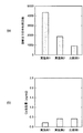
耐久性の測定結果について、図6(a)に示す。図6(a)によれば、実施例1では4300周回で、実施例2では1800周回で、比較例1では850周回でそれぞれ保護膜が破断した。膜硬度の評価結果に一致して、プラズマCVD法による非晶質窒化シリコン膜は、プラズマCVD法による非晶質カーボン膜と比べて耐摩耗性が高いことが実証された。 The durability measurement results are shown in FIG. According to FIG. 6A, the protective film was broken in 4300 rounds in Example 1, 1800 rounds in Example 2, and 850 rounds in Comparative Example 1. In agreement with the evaluation results of the film hardness, it was demonstrated that the amorphous silicon nitride film formed by the plasma CVD method has higher wear resistance than the amorphous carbon film formed by the plasma CVD method.
耐蝕性の測定結果について、図6(b)に示す。図6(b)によれば、実施例1ではCo溶出量0.2μg/m2であり、実施例2ではCo溶出量0.4μg/m2であり、比較例1ではCo溶出量0.4μg/m2であった。膜密度の評価結果と一致して、プラズマCVD法による非晶質窒化シリコン膜は、プラズマCVD法による非晶質カーボン膜と比べて耐蝕性が高いことが実証された。 FIG. 6B shows the measurement results of the corrosion resistance. According to FIG. 6B, in Example 1, the Co elution amount was 0.2 μg / m 2 , in Example 2, the Co elution amount was 0.4 μg / m 2 , and in Comparative Example 1, the Co elution amount was 0.4 μg / m 2. 2 . Consistent with the evaluation results of the film density, it was demonstrated that the amorphous silicon nitride film formed by the plasma CVD method has higher corrosion resistance than the amorphous carbon film formed by the plasma CVD method.
付着率評価について、実施例1では96%であり、実施例2では90%であり、比較例1では85%であった。プラズマCVD法による非晶質窒化シリコン膜と潤滑層であるFomblin TETRAOLとの付着が強固であることが実証された。このことは、Fomblin TETRAOLと同じフッ素含有ポリエーテルであって、末端構造が水酸基、ピペロニル基又はカルボニル基からなる分子となっている潤滑剤にも拡張できる。 Regarding the adhesion rate evaluation, it was 96% in Example 1, 90% in Example 2, and 85% in Comparative Example 1. It was proved that the adhesion between the amorphous silicon nitride film by plasma CVD method and Fomblin TETRAOL which is a lubricating layer is strong. This can be extended to a lubricant which is the same fluorine-containing polyether as Fomblin TETRAOL and whose terminal structure is a molecule composed of a hydroxyl group, a piperonyl group or a carbonyl group.
(ハードディスクドライブの構造)
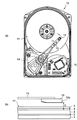
図7(a)は、本発明の実施形態に係る磁気ディスク11を搭載したハードディスクドライブ(磁気記録装置)の内部構造を示す平面図である。図7(b)は、図7(a)のI−I線に沿う断面図である。
(Hard disk drive structure)
FIG. 7A is a plan view showing the internal structure of a hard disk drive (magnetic recording apparatus) equipped with the
ハードディスクドライブは、図7(a)に示すように、筐体内に、磁気ディスク(磁気記録媒体)11と、磁気ディスク11を回転させるスピンドルモータ(図示せず)と、磁気ヘッド12と、磁気ヘッド12を支持するサスペンション13と、サスペンション13を磁気ディスク11の半径方向に駆動制御するアクチュエータ14と、スピンドルモータ及びアクチュエータ14を駆動制御するとともに磁気ヘッド12を介して磁気ディスク11に対して情報の書き込み及び読み出しを行う電子回路15とを有している。
As shown in FIG. 7A, the hard disk drive includes a magnetic disk (magnetic recording medium) 11, a spindle motor (not shown) that rotates the
磁気ディスク11は、図1に示すように、基板1上に、下層から、下地層2と、磁性層3と、保護層4と、潤滑層5とが積層されてなる。前述したように、保護層4は、N/Si比が1以上で、かつ膜密度が2.2g/cm3以上を有し、膜厚3nmで形成された非晶質窒化シリコン膜で構成されている。また、潤滑層5は、フッ素含有ポリエーテルであって末端構造が水酸基、ピペロニル基又はカルボニル基からなる分子となっている潤滑剤で構成されている。
As shown in FIG. 1, the
磁気ヘッド12は、電気信号を磁気信号に変換する書き込み素子(インダクティブヘッド)と、磁気信号を電気信号に変換する読み出し素子(磁気抵抗効果素子)とを備えている。また、磁気ディスク11は、表面には情報を記録するためのビットパターンと、トラッキング制御用のビットパターンとが設けられている。
The
このハードディスクドライブは次のように動作する。スピンドルモータにより、磁気ディスク11が高速で回転すると、磁気ディスク11の回転によって生じる空気流により、図7(b)に示すように、磁気ヘッド12は磁気ディスク11の表面から若干浮上する。このとき、磁気ディスク11の磁性層3の表面から磁気ヘッド12の記録/読取り部12aの磁気ディスク11への対向面までの距離Dを磁気スペーシングという。その状態でアクチュエータ14により磁気ヘッド12が磁気ディスク11の半径方向に移動し、磁気ディスク11に対して情報の書き込み又は読み出しが行われる。
This hard disk drive operates as follows. When the
以上のような本発明の実施形態のハードディスクドライブによれば、磁気ディスク11の保護層4である非晶質窒化シリコン膜は表面での潤滑層5の付着を強固にすることができるため、磁気ディスク11表面における磁気ヘッド12の摺動に対して保護層4からの潤滑層5の剥離が防止される。しかも、保護層4自体は、耐摩耗性(耐久性)及び耐蝕性を維持しつつ、薄膜化が可能である。さらに、保護層4は非晶質であるため多結晶の場合と異なり表面の凹凸が小さい。これにより、ハードディスクドライブは耐摩耗性(耐久性)及び耐蝕性を維持し、或いは一層高めつつ、磁気スペーシングDの短縮化、ひいては高記録密度化を図ることができる。この場合、保護層4を薄くしているため、磁気スペーシングDを短縮した場合でもフライスティクションを防止することができる。
According to the hard disk drive of the embodiment of the present invention as described above, the amorphous silicon nitride film that is the
以下、本発明の諸態様を、付記としてまとめて記載する。 Hereinafter, various aspects of the present invention will be collectively described as supplementary notes.
(付記1)基板と、前記基板の上方に形成された磁性層と、前記磁性層上に形成された密度が2.2g/cm3以上の非晶質窒化シリコン膜からなる保護層と、前記保護層上に形成された潤滑層とを有することを特徴とする磁気記録媒体。 (Appendix 1) A substrate, a magnetic layer formed above the substrate, a protective layer made of an amorphous silicon nitride film having a density of 2.2 g / cm 3 or more formed on the magnetic layer, and the protection A magnetic recording medium comprising a lubricating layer formed on the layer.
(付記2)前記保護層を構成する非晶質窒化シリコン膜は、シリコン濃度に対する窒素濃度の割合(N/Si比)が1以上であることを特徴とする付記1に記載の磁気記録媒体。
(Supplementary note 2) The magnetic recording medium according to
(付記3)前記保護層の膜厚が3nm以下であることを特徴とする付記1又は2の何れか一に記載の磁気記録媒体。
(Supplementary note 3) The magnetic recording medium according to any one of
(付記4)前記潤滑層は、フッ素含有ポリエーテルであって、該フッ素含有ポリエーテルの末端構造が水酸基、ピペロニール基、又はカルボニール基からなる分子であることを特徴とする付記1乃至3の何れか一に記載の磁気記録媒体。
(Additional remark 4) The said lubricating layer is fluorine-containing polyether, The terminal structure of this fluorine-containing polyether is a molecule | numerator which consists of a hydroxyl group, a piperonyl group, or a carbonyl group, Any of the
(付記5)付記1乃至4の何れか一に記載の磁気記録媒体と、前記磁気記録媒体の表面で浮上して、該磁気記録媒体に情報を書き込み、又は前記磁気記録媒体に記録された情報を読み出す磁気ヘッドとを有することを特徴とする磁気記録装置。
(Supplementary Note 5) Information recorded on or recorded on the magnetic recording medium according to any one of
(付記6)基板の上方に磁性層を形成する工程と、プラズマ化学気相成長法により、前記磁性層の上方に密度が2.2g/cm3以上の非晶質窒化シリコン膜からなる保護層を形成する工程と、前記保護層上に潤滑層を形成する工程とを有することを特徴とする磁気記録媒体の製造方法。 (Supplementary note 6) A protective layer made of an amorphous silicon nitride film having a density of 2.2 g / cm 3 or more is formed above the magnetic layer by a step of forming a magnetic layer above the substrate and plasma chemical vapor deposition. A method for manufacturing a magnetic recording medium, comprising: a step of forming; and a step of forming a lubricating layer on the protective layer.
(付記7)前記保護層を構成する非晶質窒化シリコン膜は、シリコン濃度に対する窒素濃度の割合(N/Si比)が1以上であることを特徴とする付記6に記載の磁気記録媒体の製造方法。 (Supplementary Note 7) The amorphous silicon nitride film constituting the protective layer has a ratio of nitrogen concentration to silicon concentration (N / Si ratio) of 1 or more. Production method.
(付記8)前記プラズマ化学気相成長法では、前記基板を加熱し、シランとアンモニアを含む成膜ガスをプラズマ化し、反応させて、前記非晶質窒化シリコン膜を形成することを特徴とする付記6又は7の何れか一に記載の磁気記録媒体の製造方法。
(Appendix 8) The plasma chemical vapor deposition method is characterized in that the substrate is heated, and a film forming gas containing silane and ammonia is converted into plasma and reacted to form the amorphous silicon nitride film. The method for manufacturing a magnetic recording medium according to any one of
(付記9)前記非晶質窒化シリコン膜を形成する間、前記基板の温度を230℃以上に保持することを特徴とする付記8記載の磁気記録媒体の製造方法。 (Supplementary note 9) The method for manufacturing a magnetic recording medium according to supplementary note 8, wherein the temperature of the substrate is maintained at 230 ° C. or higher while the amorphous silicon nitride film is formed.
1…基板、
2…下地層、
3…磁性層、
4…保護層、
5…潤滑層、
11…磁気ディスク、
12…磁気ヘッド、
12a…記録/読取り部、
D…磁気スペーシング。
1 ... substrate,
2 ... Underlayer,
3 ... magnetic layer,
4 ... protective layer,
5 ... Lubrication layer,
11 ... Magnetic disk,
12 ... Magnetic head,
12a: Recording / reading unit,
D: Magnetic spacing.
Claims (5)
前記基板の上方に形成された磁性層と、
前記磁性層の上方に形成された密度が2.2g/cm3以上の非晶質窒化シリコン膜からなる保護層と、
前記保護層上に形成された潤滑層と
を有することを特徴とする磁気記録媒体。 A substrate,
A magnetic layer formed above the substrate;
A protective layer made of an amorphous silicon nitride film having a density of 2.2 g / cm 3 or more formed above the magnetic layer;
A magnetic recording medium comprising a lubricating layer formed on the protective layer.
前記磁気記録媒体に情報を書き込み、又は前記磁気記録媒体に記録された情報を読み出す磁気ヘッドと
を有することを特徴とする磁気記録装置。 A magnetic recording medium according to any one of claims 1 to 3,
A magnetic recording apparatus comprising: a magnetic head for writing information on the magnetic recording medium or reading information recorded on the magnetic recording medium.
プラズマ化学気相成長法により、前記磁性層の上方に密度が2.2g/cm3以上の非晶質窒化シリコン膜からなる保護層を形成する工程と、
前記保護層上に潤滑層を形成する工程と
を有することを特徴とする磁気記録媒体の製造方法。 Forming a magnetic layer above the substrate;
Forming a protective layer made of an amorphous silicon nitride film having a density of 2.2 g / cm 3 or more above the magnetic layer by plasma enhanced chemical vapor deposition;
And a step of forming a lubricating layer on the protective layer.
Priority Applications (1)
| Application Number | Priority Date | Filing Date | Title |
|---|---|---|---|
| JP2007219424A JP2009054228A (en) | 2007-08-27 | 2007-08-27 | Magnetic recording medium, manufacturing method thereof, and magnetic recording unit |
Applications Claiming Priority (1)
| Application Number | Priority Date | Filing Date | Title |
|---|---|---|---|
| JP2007219424A JP2009054228A (en) | 2007-08-27 | 2007-08-27 | Magnetic recording medium, manufacturing method thereof, and magnetic recording unit |
Publications (1)
| Publication Number | Publication Date |
|---|---|
| JP2009054228A true JP2009054228A (en) | 2009-03-12 |
Family
ID=40505178
Family Applications (1)
| Application Number | Title | Priority Date | Filing Date |
|---|---|---|---|
| JP2007219424A Withdrawn JP2009054228A (en) | 2007-08-27 | 2007-08-27 | Magnetic recording medium, manufacturing method thereof, and magnetic recording unit |
Country Status (1)
| Country | Link |
|---|---|
| JP (1) | JP2009054228A (en) |
Cited By (1)
| Publication number | Priority date | Publication date | Assignee | Title |
|---|---|---|---|---|
| JP2018034407A (en) * | 2016-08-31 | 2018-03-08 | 東芝ホクト電子株式会社 | Thermal print head and thermal printer |
-
2007
- 2007-08-27 JP JP2007219424A patent/JP2009054228A/en not_active Withdrawn
Cited By (1)
| Publication number | Priority date | Publication date | Assignee | Title |
|---|---|---|---|---|
| JP2018034407A (en) * | 2016-08-31 | 2018-03-08 | 東芝ホクト電子株式会社 | Thermal print head and thermal printer |
Similar Documents
| Publication | Publication Date | Title |
|---|---|---|
| JP5360894B2 (en) | Method for manufacturing magnetic recording medium | |
| JP5401066B2 (en) | Magnetic disk and manufacturing method thereof | |
| US20130114165A1 (en) | FePt-C BASED MAGNETIC RECORDING MEDIA WITH ONION-LIKE CARBON PROTECTION LAYER | |
| JP4839723B2 (en) | Protective film forming method and magnetic recording medium provided with the protective film | |
| JP4943972B2 (en) | Storage medium and storage device | |
| US20090226767A1 (en) | Substrate for magnetic recording medium, magnetic recording medium, and magnetic recording and reproducing apparatus | |
| US8472134B2 (en) | Air bearing surface overcoat with soft intermediate film, and methods of producing the same | |
| JP2013182640A (en) | Magnetic recording medium and method of manufacturing the same, and magnetic memory using the same | |
| US8767350B2 (en) | Magnetic recording medium having recording regions and separating regions and methods of manufacturing the same | |
| JP4718797B2 (en) | Magnetic recording medium and magnetic recording apparatus | |
| JP2006277779A (en) | Magnetic recording medium and magnetic recording apparatus | |
| JP2014056633A (en) | Method for manufacturing magnetic recording medium | |
| JP2009054228A (en) | Magnetic recording medium, manufacturing method thereof, and magnetic recording unit | |
| US20110032640A1 (en) | Multi-layer, thin film overcoat for magnetic media disk | |
| JP5578800B2 (en) | Manufacturing method of magnetic disk | |
| JP2011192320A (en) | Perpendicular magnetic recording medium | |
| US20110058279A1 (en) | Overcoat having a low silicon/carbon ratio | |
| JP2008052833A (en) | Magnetic recording medium and manufacturing method therefor | |
| JP5786047B2 (en) | Magnetic medium with low molecular weight lubricant layer for use in head / medium contact detection | |
| JP2008276912A (en) | Vertical magnetic recording medium and its manufacturing method | |
| JPWO2010038754A1 (en) | Method for manufacturing magnetic recording medium and magnetic recording medium | |
| JP2001060305A (en) | Magnetic recording and reproducing device | |
| JP2001034925A (en) | Magnetic recording medium | |
| JP2008090900A (en) | Magnetic recording medium and manufacturing method therefor | |
| JP2009283036A (en) | Method of manufacturing magnetic recording medium |
Legal Events
| Date | Code | Title | Description |
|---|---|---|---|
| A300 | Withdrawal of application because of no request for examination |
Free format text: JAPANESE INTERMEDIATE CODE: A300 Effective date: 20101102 |